JP5574667B2 - Package, semiconductor device, manufacturing method and equipment thereof - Google Patents
Package, semiconductor device, manufacturing method and equipment thereofDownload PDFInfo
- Publication number
- JP5574667B2 JP5574667B2JP2009242784AJP2009242784AJP5574667B2JP 5574667 B2JP5574667 B2JP 5574667B2JP 2009242784 AJP2009242784 AJP 2009242784AJP 2009242784 AJP2009242784 AJP 2009242784AJP 5574667 B2JP5574667 B2JP 5574667B2
- Authority
- JP
- Japan
- Prior art keywords
- lead
- frame member
- semiconductor element
- side wall
- package
- Prior art date
- Legal status (The legal status is an assumption and is not a legal conclusion. Google has not performed a legal analysis and makes no representation as to the accuracy of the status listed.)
- Expired - Fee Related
Links
Images


Classifications
- H—ELECTRICITY
- H10—SEMICONDUCTOR DEVICES; ELECTRIC SOLID-STATE DEVICES NOT OTHERWISE PROVIDED FOR
- H10F—INORGANIC SEMICONDUCTOR DEVICES SENSITIVE TO INFRARED RADIATION, LIGHT, ELECTROMAGNETIC RADIATION OF SHORTER WAVELENGTH OR CORPUSCULAR RADIATION
- H10F39/00—Integrated devices, or assemblies of multiple devices, comprising at least one element covered by group H10F30/00, e.g. radiation detectors comprising photodiode arrays
- H10F39/80—Constructional details of image sensors
- H10F39/804—Containers or encapsulations
- H—ELECTRICITY
- H01—ELECTRIC ELEMENTS
- H01L—SEMICONDUCTOR DEVICES NOT COVERED BY CLASS H10
- H01L23/00—Details of semiconductor or other solid state devices
- H01L23/48—Arrangements for conducting electric current to or from the solid state body in operation, e.g. leads, terminal arrangements ; Selection of materials therefor
- H01L23/488—Arrangements for conducting electric current to or from the solid state body in operation, e.g. leads, terminal arrangements ; Selection of materials therefor consisting of soldered or bonded constructions
- H01L23/498—Leads, i.e. metallisations or lead-frames on insulating substrates, e.g. chip carriers
- H01L23/49861—Lead-frames fixed on or encapsulated in insulating substrates
- H—ELECTRICITY
- H10—SEMICONDUCTOR DEVICES; ELECTRIC SOLID-STATE DEVICES NOT OTHERWISE PROVIDED FOR
- H10F—INORGANIC SEMICONDUCTOR DEVICES SENSITIVE TO INFRARED RADIATION, LIGHT, ELECTROMAGNETIC RADIATION OF SHORTER WAVELENGTH OR CORPUSCULAR RADIATION
- H10F39/00—Integrated devices, or assemblies of multiple devices, comprising at least one element covered by group H10F30/00, e.g. radiation detectors comprising photodiode arrays
- H10F39/011—Manufacture or treatment of image sensors covered by group H10F39/12
- H—ELECTRICITY
- H01—ELECTRIC ELEMENTS
- H01L—SEMICONDUCTOR DEVICES NOT COVERED BY CLASS H10
- H01L2224/00—Indexing scheme for arrangements for connecting or disconnecting semiconductor or solid-state bodies and methods related thereto as covered by H01L24/00
- H01L2224/01—Means for bonding being attached to, or being formed on, the surface to be connected, e.g. chip-to-package, die-attach, "first-level" interconnects; Manufacturing methods related thereto
- H01L2224/42—Wire connectors; Manufacturing methods related thereto
- H01L2224/44—Structure, shape, material or disposition of the wire connectors prior to the connecting process
- H01L2224/45—Structure, shape, material or disposition of the wire connectors prior to the connecting process of an individual wire connector
- H01L2224/45001—Core members of the connector
- H01L2224/45099—Material
- H01L2224/451—Material with a principal constituent of the material being a metal or a metalloid, e.g. boron (B), silicon (Si), germanium (Ge), arsenic (As), antimony (Sb), tellurium (Te) and polonium (Po), and alloys thereof
- H01L2224/45117—Material with a principal constituent of the material being a metal or a metalloid, e.g. boron (B), silicon (Si), germanium (Ge), arsenic (As), antimony (Sb), tellurium (Te) and polonium (Po), and alloys thereof the principal constituent melting at a temperature of greater than or equal to 400°C and less than 950°C
- H01L2224/45124—Aluminium (Al) as principal constituent
- H—ELECTRICITY
- H01—ELECTRIC ELEMENTS
- H01L—SEMICONDUCTOR DEVICES NOT COVERED BY CLASS H10
- H01L2224/00—Indexing scheme for arrangements for connecting or disconnecting semiconductor or solid-state bodies and methods related thereto as covered by H01L24/00
- H01L2224/01—Means for bonding being attached to, or being formed on, the surface to be connected, e.g. chip-to-package, die-attach, "first-level" interconnects; Manufacturing methods related thereto
- H01L2224/42—Wire connectors; Manufacturing methods related thereto
- H01L2224/44—Structure, shape, material or disposition of the wire connectors prior to the connecting process
- H01L2224/45—Structure, shape, material or disposition of the wire connectors prior to the connecting process of an individual wire connector
- H01L2224/45001—Core members of the connector
- H01L2224/45099—Material
- H01L2224/451—Material with a principal constituent of the material being a metal or a metalloid, e.g. boron (B), silicon (Si), germanium (Ge), arsenic (As), antimony (Sb), tellurium (Te) and polonium (Po), and alloys thereof
- H01L2224/45138—Material with a principal constituent of the material being a metal or a metalloid, e.g. boron (B), silicon (Si), germanium (Ge), arsenic (As), antimony (Sb), tellurium (Te) and polonium (Po), and alloys thereof the principal constituent melting at a temperature of greater than or equal to 950°C and less than 1550°C
- H01L2224/45144—Gold (Au) as principal constituent
- H—ELECTRICITY
- H01—ELECTRIC ELEMENTS
- H01L—SEMICONDUCTOR DEVICES NOT COVERED BY CLASS H10
- H01L2224/00—Indexing scheme for arrangements for connecting or disconnecting semiconductor or solid-state bodies and methods related thereto as covered by H01L24/00
- H01L2224/01—Means for bonding being attached to, or being formed on, the surface to be connected, e.g. chip-to-package, die-attach, "first-level" interconnects; Manufacturing methods related thereto
- H01L2224/42—Wire connectors; Manufacturing methods related thereto
- H01L2224/47—Structure, shape, material or disposition of the wire connectors after the connecting process
- H01L2224/48—Structure, shape, material or disposition of the wire connectors after the connecting process of an individual wire connector
- H01L2224/481—Disposition
- H01L2224/48151—Connecting between a semiconductor or solid-state body and an item not being a semiconductor or solid-state body, e.g. chip-to-substrate, chip-to-passive
- H01L2224/48221—Connecting between a semiconductor or solid-state body and an item not being a semiconductor or solid-state body, e.g. chip-to-substrate, chip-to-passive the body and the item being stacked
- H01L2224/48245—Connecting between a semiconductor or solid-state body and an item not being a semiconductor or solid-state body, e.g. chip-to-substrate, chip-to-passive the body and the item being stacked the item being metallic
- H01L2224/48247—Connecting between a semiconductor or solid-state body and an item not being a semiconductor or solid-state body, e.g. chip-to-substrate, chip-to-passive the body and the item being stacked the item being metallic connecting the wire to a bond pad of the item
- H—ELECTRICITY
- H01—ELECTRIC ELEMENTS
- H01L—SEMICONDUCTOR DEVICES NOT COVERED BY CLASS H10
- H01L24/00—Arrangements for connecting or disconnecting semiconductor or solid-state bodies; Methods or apparatus related thereto
- H01L24/01—Means for bonding being attached to, or being formed on, the surface to be connected, e.g. chip-to-package, die-attach, "first-level" interconnects; Manufacturing methods related thereto
- H01L24/42—Wire connectors; Manufacturing methods related thereto
- H01L24/44—Structure, shape, material or disposition of the wire connectors prior to the connecting process
- H01L24/45—Structure, shape, material or disposition of the wire connectors prior to the connecting process of an individual wire connector
- H—ELECTRICITY
- H01—ELECTRIC ELEMENTS
- H01L—SEMICONDUCTOR DEVICES NOT COVERED BY CLASS H10
- H01L24/00—Arrangements for connecting or disconnecting semiconductor or solid-state bodies; Methods or apparatus related thereto
- H01L24/01—Means for bonding being attached to, or being formed on, the surface to be connected, e.g. chip-to-package, die-attach, "first-level" interconnects; Manufacturing methods related thereto
- H01L24/42—Wire connectors; Manufacturing methods related thereto
- H01L24/47—Structure, shape, material or disposition of the wire connectors after the connecting process
- H01L24/48—Structure, shape, material or disposition of the wire connectors after the connecting process of an individual wire connector
- H—ELECTRICITY
- H01—ELECTRIC ELEMENTS
- H01L—SEMICONDUCTOR DEVICES NOT COVERED BY CLASS H10
- H01L2924/00—Indexing scheme for arrangements or methods for connecting or disconnecting semiconductor or solid-state bodies as covered by H01L24/00
- H01L2924/15—Details of package parts other than the semiconductor or other solid state devices to be connected
- H01L2924/161—Cap
- H01L2924/1615—Shape
- H01L2924/16195—Flat cap [not enclosing an internal cavity]
- H—ELECTRICITY
- H01—ELECTRIC ELEMENTS
- H01L—SEMICONDUCTOR DEVICES NOT COVERED BY CLASS H10
- H01L2924/00—Indexing scheme for arrangements or methods for connecting or disconnecting semiconductor or solid-state bodies as covered by H01L24/00
- H01L2924/15—Details of package parts other than the semiconductor or other solid state devices to be connected
- H01L2924/161—Cap
- H01L2924/162—Disposition
- H01L2924/16235—Connecting to a semiconductor or solid-state bodies, i.e. cap-to-chip
- H—ELECTRICITY
- H01—ELECTRIC ELEMENTS
- H01L—SEMICONDUCTOR DEVICES NOT COVERED BY CLASS H10
- H01L2924/00—Indexing scheme for arrangements or methods for connecting or disconnecting semiconductor or solid-state bodies as covered by H01L24/00
- H01L2924/15—Details of package parts other than the semiconductor or other solid state devices to be connected
- H01L2924/181—Encapsulation
Landscapes
- Physics & Mathematics (AREA)
- Condensed Matter Physics & Semiconductors (AREA)
- General Physics & Mathematics (AREA)
- Engineering & Computer Science (AREA)
- Computer Hardware Design (AREA)
- Microelectronics & Electronic Packaging (AREA)
- Power Engineering (AREA)
- Lead Frames For Integrated Circuits (AREA)
- Solid State Image Pick-Up Elements (AREA)
Description
Translated fromJapanese本発明は、半導体素子を搭載するためのパッケージ、半導体装置、それらの製造方法及び機器に関する。The present invention relates to a package for mounting a semiconductor element, asemiconductor device, a manufacturing methodthereof ,and an apparatus .
半導体装置において、半導体素子を搭載するためにリードフレームを利用して形成されるプラスチックパッケージが広く用いられている。近年、出力電気信号のデジタル化により入出力信号線数が増加しており、それに伴い、パッケージの入出力端子数も増加させる必要が出てきている。また、半導体装置を搭載する機器の小型化に伴い、パッケージの小型化も求められている。一般的にリードフレームを利用して形成されるパッケージでは、入出力端子がパッケージの外周に沿って形成されている。そのため、入出力端子数を増加させようとするとパッケージの外周を大きくせざるを得ず、その結果としてパッケージも大型化してしまう。この問題を解決するために、特許文献1はLGA(Land Grid Array)タイプのパッケージを提案している。LGAタイプのパッケージでは、リードフレームを波状にプレス成形して、波状の上側を切断してから樹脂成形することによって、パッケージの裏面に入出力端子が形成される。 In a semiconductor device, a plastic package formed by using a lead frame for mounting a semiconductor element is widely used. In recent years, the number of input / output signal lines has increased due to the digitization of output electric signals, and accordingly, the number of input / output terminals of a package has to be increased. In addition, with the miniaturization of devices on which semiconductor devices are mounted, there is a demand for miniaturization of packages. In a package generally formed using a lead frame, input / output terminals are formed along the outer periphery of the package. For this reason, if the number of input / output terminals is to be increased, the outer periphery of the package must be enlarged, and as a result, the package also becomes larger. In order to solve this problem,
しかしながら、LGAタイプのように端子がランド形状である場合には入出力端子の下面のみでの半田接合となるため、半田接合性が低下し、使用用途、実装基板の種類によっては半田接合の信頼性が低下する可能性がある。そこで、本発明は、端子数の増加と半田接合の信頼性の向上とを実現する技術を提供することを目的とする。 However, when the terminal has a land shape as in the LGA type, solder bonding is performed only on the lower surface of the input / output terminal, so that the solder bonding performance is lowered, and the reliability of solder bonding depends on the application and type of mounting board. May be reduced. Therefore, an object of the present invention is to provide a technique for realizing an increase in the number of terminals and an improvement in the reliability of solder bonding.
上記課題に鑑みて、本発明に係るパッケージは、半導体素子を搭載するためのパッケージであって、枠部材と、前記半導体素子との接続に用いられる第1の部分、及び、前記枠部材の外側の側壁から突出し実装基板との接続に用いられる部分を有する第1のリードと、前記半導体素子との接続に用いられる第2の部分、及び、前記枠部材の内側の側壁から突出し実装基板との接続に用いられる部分を有する第2のリードとを備え、前記外側の側壁に沿って複数の前記第1のリードが設けられ、前記内側の側壁に沿って複数の前記第2のリードが設けられ、前記外側の側壁と前記内側の側壁との間に前記第1の部分及び前記第2の部分が位置しており、前記外側の側壁から前記第1のリードの前記突出した部分の先端とは反対側の先端までの距離が、前記外側の側壁から前記第2のリードの前記突出した部分の先端とは反対側の先端までの距離よりも小さいことを特徴とする。
本発明に係る半導体装置は、枠部材と、前記枠部材の外側の側壁よりも内側に配置され半導体素子と、ボンディングワイヤによって前記半導体素子に接続された第1の部分、及び、前記枠部材の外側の側壁から突出し実装基板との接続に用いられる部分を有する第1のリードと、ボンディングワイヤによって前記半導体素子に接続された第2の部分、及び、前記枠部材の内側の側壁から突出し実装基板との接続に用いられる部分を有する第2のリードと、を備えることを特徴とする。
本発明に係る半導体素子を搭載するためのパッケージの製造方法は、外側支持部から内側に延びる第1のリードと、前記外側支持部の内側に位置する内側支持部から外側に前記第1のリードの先端に向かって延びる第2のリードとを有するリードフレームの上に、開口部を有する枠部材を、前記第1のリードの外側の部分が前記枠部材の外側において露出し、且つ前記第2のリードの内側の部分が前記開口部において露出するように形成する工程と、前記第1のリードから前記外側支持部を切り離し、前記第2のリードから前記内側支持部を切り離す工程とを有することを特徴とする。
本発明に係る半導体装置の製造方法は、外側支持部から内側に延びる第1のリードと、前記外側支持部の内側に位置する内側支持部から外側に延びる第2のリードとを有するリードフレームの上に、開口部を有する枠部材を、前記第1のリードの外側の部分が前記枠部材の外側において露出し、且つ前記第2のリードの内側の部分が前記開口部において露出するように形成する工程と、前記第1のリードから前記外側支持部を切り離し、前記第2のリードから前記内側支持部を切り離す工程と、前記開口部を覆う位置に半導体素子を配置する工程と、前記半導体素子をボンディングワイヤによって前記第1のリード及び前記第2のリードに接続する工程とを有することを特徴とする。In view of the above problems, a package according to the present invention is a package for mounting a semiconductor element, andincludes a frame member, a first portionused for connectionwith the semiconductor element, and an outside of the frame member. of a first lead having a portionused for connection with the projectingmounting board from the side wall, the second portionused for connectionto the semiconductorelement,and,with projectingmounting board from inside of the side wall of said frame memberA second lead havinga portionused for connection,a plurality of the first leads are provided along the outer side wall, and a plurality of the second leads are provided along the inner side wall. The first portion and the second portion are located between the outer side wall and the inner side wall, and a tip of the protruding portion of the first lead from the outer side wall Distance to the tip on the opposite side But wherein from the outside of the side wall and the tip of the projecting portion of the second lead to beingless than the distance to the tip of the opposite side.
A semiconductor device according to the present invention includes a frame member, a semiconductor element disposed inside the outer side wall of the frame member, a first portion connected to the semiconductor element by a bonding wire, and the frame member A first lead having a portion protruding from the outer side wall and used for connection to the mounting substrate, a second portion connected to the semiconductor element by a bonding wire, and a mounting substrate protruding from the inner side wall of the frame member And a second lead having a portion used for connection to.
A method of manufacturing a package for mounting a semiconductor device according to the present invention includes: a first lead extending inward from an outer support portion; and the first lead outward from an inner support portion positioned inside the outer support portion. A frame member having an opening on a lead frame having a second lead extending toward the tip of the first lead, and an outer portion of the first lead is exposed outside the frame member; Forming an inner portion of the lead so as to be exposed at the opening, and separating the outer support from the first lead and separating the inner support from the second lead. It is characterized by.
According to another aspect of the present invention, there is provided a method for manufacturing a semiconductor device, comprising: a first lead that extends inward from an outer support; and a second lead that extends outward from an inner support located inside the outer support. A frame member having an opening is formed so that an outer portion of the first lead is exposed outside the frame member and an inner portion of the second lead is exposed at the opening. A step of separating the outer support portion from the first lead, a step of separating the inner support portion from the second lead, a step of disposing a semiconductor element at a position covering the opening, and the semiconductor element Connecting the first lead and the second lead with a bonding wire.
上記手段により、端子数の増加と半田接合の信頼性の向上とを実現する技術が提供される。 By the above means, a technique for realizing an increase in the number of terminals and an improvement in the reliability of solder bonding is provided.
添付の図面を参照しつつ、本発明の実施形態を以下に説明する。 Embodiments of the present invention will be described below with reference to the accompanying drawings.
<第1の実施形態>
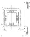
図1を用いて本実施形態のパッケージ100の一例を説明する。図1(a)はパッケージ100の平面図を示し、図1(b)はパッケージ100のA−A´断面図を示す。パッケージ100は、第1のリード1、第2のリード2、及び枠部材3を備える。本実施形態の枠部材3は互いに隣接した内周部3aと外周部3bとを有し、内周部3aの高さよりも外周部3bの高さが高い凹状の形状となっている。枠部材3は、例えば樹脂で形成される。枠部材3は内周部3aに開口部4を有し、開口部4により枠部材3は上下方向に貫通している。本明細書では、半導体素子が搭載される側を上方向とし、基板側を下方向とする。枠部材3には、外周部に複数の第1のリード1が形成されており、内周部に複数の第2のリード2が形成されている。<First Embodiment>
An example of the
第1のリード1は、パッケージ100に搭載される半導体素子との接続に用いられる露出部1aと、実装基板との接続に用いられる突出部1bとを有する。露出部1aは枠部材3の上面において露出しており、露出部1aに半導体素子が電気的に接続される。突出部1bは枠部材3の外側の側壁から外側に突出している。突出部1bを用いて第1のリード1は実装基板に半田接合される。 The
第2のリード2は、パッケージ100に搭載される半導体素子との接続に用いられる露出部2aと、実装基板との接続に用いられる突出部2bとを有する。露出部2aは枠部材3の上面において露出しており、露出部2aに半導体素子が電気的に接続される。突出部2bは枠部材3の内側の側壁から開口部4の内側に突出している。突出部2bを用いて第2のリード2は実装基板に半田接合される。本実施形態では、パッケージ100が第2のリード2を有するため、パッケージ100のサイズを大きくすることなく、端子数を増やすことが可能となる。 The
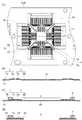
続いて、図2を用いて、パッケージ100に半導体素子を搭載した半導体装置の一例を説明する。本実施形態では、半導体素子として固体撮像素子チップ6を用いた固体撮像装置200を例として扱う。しかしながら、パッケージ100に電気的に接続可能な半導体素子であれば、いかなるものであっても本発明を適用できる。図2(a)は実装基板10に搭載された固体撮像装置200の断面図であり、図2(b)は突出部1bを矢印5の方向から見た部分断面図である。 Next, an example of a semiconductor device in which a semiconductor element is mounted on the
パッケージ100の上に、開口部4を覆うように固体撮像素子チップ6が搭載される。本実施形態では、固体撮像素子チップ6が開口部4を完全に覆うように、開口部4が固体撮像素子チップ6よりも小さくなっている。しかしながら、固体撮像素子チップ6は開口部4よりも小さくてもよく、また固体撮像素子チップ6が開口部4の一部を覆ってもよい。固体撮像素子チップ6と比較して開口部4が小さいほど固体撮像素子チップ6をパッケージ100に搭載する際の接着領域が広くなり、接着が容易となる。一方、開口部4が大きいほど、第2のリード2の干渉を避けつつ、第2のリード2の本数を増やすことができる。従って、開口部4の大きさは必要な入出力端子数に応じて選択される。例えば、開口部4の大きさは固体撮像素子チップ6の50〜90%程度の大きさとするとよい。 A solid-state
固体撮像素子チップ6は、金やアルミ等の金属細線であるボンディングワイヤ9によって、露出部1a、2aと電気的に接続されている。また、固体撮像素子チップ6上には、受光領域7を取り囲むように封止枠11が接着される。さらに封止枠11上にガラスや水晶等の透明部材8が接着されており、それにより受光領域7が気密封止されている。ボンディングワイヤ9及び固体撮像素子チップ6の外周部は、封止樹脂12によって被覆されている。 The solid-state
突出部1b、2bは、半田13によって実装基板10に半田接合されている。図2(b)に示すように、突出部1bの全周囲にわたって半田13が濡れ広がっている。また、突出部2bについても同様に半田13を濡れ広がっている。そのため、本実施形態のパッケージ100は信頼性の高い半田接合を実現する。さらに、本実施形態の固体撮像装置200は、固体撮像素子チップ6の裏面が露出するとともに、固体撮像素子チップ6と実装基板10との間にスペースが形成されている。そのため、このスペースに放熱部品を設置することが可能であり、さらには固体撮像素子チップ6から直接放熱させることができるため、従来のLGAタイプの半導体装置と比較して放熱性を向上できる。 The protruding
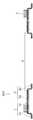
続いて、図3を用いて、パッケージ100の製造方法を説明する。図3(b)から図3(d)は図3(a)のB−B′断面図である。まず、図3(a)に示されるリードフレーム300を生成する。リードフレーム300は、外側支持部14と、外側支持部14の内側にある内側支持部15とを備える。内側支持部15は、吊りリード16を介して外側支持部14により連結支持されている。外側支持部14からは第1のリード1が内側に延びており、内側支持部15からは第2のリード2が外側に延びている。第1のリード1の内側の部分が露出部1aとなり、外側の部分が突出部1bとなる。第2のリード2の外側の部分が露出部2aとなり、内側の部分が突出部2bとなる。リードフレーム300は金型を用いた打ち抜き加工又はウェットエッチング加工などの既存の方法を用いて形成される。 Next, a method for manufacturing the
次に、図3(b)に示すように、第1のリード1及び第2のリード2に段差を形成するための曲げ加工を行う。第1のリード1は、露出部1aと突出部1bとの間で曲げられる。第2のリード2は、露出部2aと突出部2bとの間で曲げられる。曲げ量や段差量については適宜選択する。例えば、段差量を大きくとった場合には、半導体素子を搭載した場合に、半導体素子の下のスペースを大きくとることが可能である。空間スペースを大きくとることによって、より大きな放熱部品を設置することが可能となる。 Next, as shown in FIG. 3B, a bending process for forming a step in the
次に、図3(c)に示すように、リードフレーム300の上に、開口部4を有する凹状の枠部材3を成形する。枠部材3は、第1のリード1の外側の部分が枠部材3の外側に露出し、かつ第2のリード2の内側の部分が開口部4に露出するように形成される。枠部材3の加工方法として、金型を用いた樹脂成形、例えば、トランスファー成形、射出成形などが利用できる。また、枠部材3の材料は、熱硬化性樹脂、熱可塑性樹脂など既存の樹脂が利用できる。 Next, as shown in FIG. 3C, the
最後に、図3(d)に示すように、第1のリード1から外側支持部14を切り離し、第2のリード2から内側支持部15を切り離す。さらに、第1のリード1同士を接続しているフレーム部分を切除し、第2のリード2同士を接続しているフレーム部分を切除する。これにより、突出部1b、2bがそれぞれ形成される。突出部1b、2bの長さは例えば0.3mm〜0.5mmとするとよい。 Finally, as shown in FIG. 3D, the
以上のように、本実施形態によれば、端子数の増加と半田接合の信頼性の向上とを実現する技術が提供される。 As described above, according to the present embodiment, a technique for increasing the number of terminals and improving the reliability of solder bonding is provided.
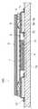
<第2の実施形態>
図4を用いて本実施形態のパッケージ400の一例を説明する。図4はパッケージ400の断面図を表す。パッケージ400の平面図は、図1(a)に示された第1の実施形態のパッケージ100の平面図と同様であるため省略する。パッケージ400は、突出部1c、2cの形状が第1の実施形態のパッケージ100と異なる。パッケージ400では、突出部1c、2cは折り曲げ加工が施されており、ガルウイング状となっている。すなわち、枠部材3から見た場合に、突出部1c、2cは水平方向遠方に延び、一度折れ曲がって枠部材3の下方向に延び、さらにもう一度折れ曲がって水平方向遠方に延びる。折り曲げ加工の形状については、ガルウイング状に限定されるものではなく、突出部1c、2cの先端が枠部材3の下面よりも下に位置するように、突出部1c、2cが曲がっていればよい。<Second Embodiment>
An example of the
この形状により、第1の実施形態のパッケージ100と比べて、開口部4の下側のスペースをさらに広くすることが可能となる。従って、パッケージ100と比べて、より大きな放熱部品を半導体素子と実装基板との間に配置することが可能となり、より放熱性を要求する半導体素子を搭載することが可能となる。また、パッケージ400についても、突出部1c、2cに半田を濡れ広げさせることができ、信頼性の高い半田接合が可能である。 This shape makes it possible to further widen the space below the
続いて、図5を用いて、パッケージ400に半導体素子を搭載した半導体装置の一例を説明する。本実施形態でも、半導体素子として固体撮像素子チップ6を用いた固体撮像装置500を例として扱う。図5は実装基板10に搭載された固体撮像装置500の断面図である。第1の実施形態と同様に、固体撮像素子チップ6が開口部4を覆うようにパッケージ400に搭載される。固体撮像素子チップ6と露出部1a、2aとはボンディングワイヤ9により接続される。枠部材3の上にはさらに透明部材8が接着され、固体撮像素子チップ6及びボンディングワイヤ9が気密封止されている。突出部1c、2cの先端は、半田13によって実装基板10に半田接合されている。 Next, an example of a semiconductor device in which a semiconductor element is mounted on the
さらに、固体撮像装置500は、固体撮像素子チップ6の下のスペースに放熱部品17を備える。放熱部品17は例えば板状やフィン形状の金属板などである。突出部1c、2cがガルウイング状をしているため、図5に示すように、放熱部品17は固体撮像素子チップ6と実装基板10との間に収まる。放熱部品17は、固体撮像素子チップ6の裏面に直接接着することができるため、固体撮像素子チップ6の発熱を効率良く放熱することが可能である。実装基板10上に放熱用の配線が施されていれは、放熱性能はさらに向上する。 Further, the solid-
パッケージ400の製造方法は、第1の実施形態のパッケージ100の製造方法において、図3(b)に示した曲げ加工を行う代わりに、突出部1c、2cの曲げ加工を行う。この曲げ加工により、ガルウイング状の突出部1c、2cが形成される。 The manufacturing method of the
以上のように、本実施形態によれば、端子数の増加と半田接合の信頼性の向上とを実現する技術が提供される。さらに、本実施形態によれば、放熱性を向上させることが可能となる。 As described above, according to the present embodiment, a technique for increasing the number of terminals and improving the reliability of solder bonding is provided. Furthermore, according to this embodiment, it is possible to improve heat dissipation.
<第3の実施形態>
図6を用いて本実施形態のパッケージ600の一例を説明する。図6はパッケージ600の断面図を表す。パッケージ600の平面図は、図1(a)に示された第1の実施形態のパッケージ100の平面図と同様であるため省略する。パッケージ600は、突出部1d、2dの形状が第1の実施形態のパッケージ100と異なる。パッケージ400では、突出部1d、2dは折り曲げ加工が施されており、DIPタイプやSIPタイプと同様に、搭載される半導体素子に対して垂直な方向に突出部1d、2dの先端が向いている。<Third Embodiment>
An example of the package 600 of this embodiment will be described with reference to FIG. FIG. 6 shows a cross-sectional view of the package 600. The plan view of the package 600 is the same as the plan view of the
続いて、図7を用いて、パッケージ600に半導体素子を搭載した半導体装置の一例を説明する。本実施形態でも、半導体素子として固体撮像素子チップ6を用いた固体撮像装置700を例として扱う。図7は実装基板10に搭載された固体撮像装置700の断面図である。第2の実施形態で説明した固体撮像装置500と同様の部分については説明を省略する。突出部1d、2dは実装基板10に垂直に挿入され、実装基板10の裏面で半田接合される。したがって、表面実装する場合に比べて、実装基板10の反りや変形に対してさらに信頼性の高い半田接合が得られる。さらに、突出部1d、2dの長さや実装基板10への挿入量によってパッケージ600の下面と実装基板10との間隔を自由に調整できる。従って、パッケージ600の下面のスペースに配置される放熱部品17などの部品の形状、大きさなどの自由度が増える。 Next, an example of a semiconductor device in which a semiconductor element is mounted on the package 600 will be described with reference to FIG. Also in this embodiment, the solid-
パッケージ600の製造方法は第2の実施形態で説明したパッケージ400の製造方法と同様のため説明を省略する。 Since the manufacturing method of the package 600 is the same as the manufacturing method of the
以上のように、本実施形態によれば、端子数の増加と半田接合の信頼性の向上とを実現する技術が提供される。さらに、本実施形態によれば、放熱性を向上させることが可能となる。 As described above, according to the present embodiment, a technique for increasing the number of terminals and improving the reliability of solder bonding is provided. Furthermore, according to this embodiment, it is possible to improve heat dissipation.
Claims (13)
Translated fromJapanese枠部材と、
前記半導体素子との接続に用いられる第1の部分、及び、前記枠部材の外側の側壁から突出し実装基板との接続に用いられる部分を有する第1のリードと、
前記半導体素子との接続に用いられる第2の部分、及び、前記枠部材の内側の側壁から突出し実装基板との接続に用いられる部分を有する第2のリードと
を備え、
前記外側の側壁に沿って複数の前記第1のリードが設けられ、前記内側の側壁に沿って複数の前記第2のリードが設けられ、前記外側の側壁と前記内側の側壁との間に前記第1の部分及び前記第2の部分が位置しており、
前記外側の側壁から前記第1のリードの前記突出した部分の先端とは反対側の先端までの距離が、前記外側の側壁から前記第2のリードの前記突出した部分の先端とは反対側の先端までの距離よりも小さいことを特徴とするパッケージ。A package for mounting a semiconductor element,
A frame member;
Said first portionused for connectionwith the semiconductorelement, anda first lead having a portionused for connection with the projectingmounting substrate from a side wall of the outer of said frame member,
A second portionused for connectionto the semiconductorelement,and, a second lead having a portionused for connection with the projectingmounting board from inside of the side wall of said framemember,
A plurality of the first leads are provided along the outer side wall, a plurality of the second leads are provided along the inner side wall, and the plurality of second leads are provided between the outer side wall and the inner side wall. The first part and the second part are located;
The distance from the outer side wall to the tip of the protruding portion of the first lead opposite to the tip of the protruding portion is opposite to the tip of the protruding portion of the second lead from the outer side wall. A package characterizedby being smaller than the distance to the tip .
前記枠部材の前記外側の側壁よりも内側に配置され、前記第1のリードの前記第1の部分及び前記第2のリードの前記第2の部分に接続された半導体素子と
を備えることを特徴とする半導体装置。A package according to any one of claims 1 to 3;
And a semiconductor element disposed on theinner side of the outer side wall of the frame member and connected to the first portion of the first lead and the second portion of the second lead. A semiconductor device.
前記枠部材の外側の側壁よりも内側に配置され半導体素子と、 A semiconductor element disposed on the inner side of the outer side wall of the frame member;
ボンディングワイヤによって前記半導体素子に接続された第1の部分、及び、前記枠部材の外側の側壁から突出し実装基板との接続に用いられる部分を有する第1のリードと、 A first lead connected to the semiconductor element by a bonding wire, and a first lead having a part protruding from an outer side wall of the frame member and used for connection to a mounting substrate;
ボンディングワイヤによって前記半導体素子に接続された第2の部分、及び、前記枠部材の内側の側壁から突出し実装基板との接続に用いられる部分を有する第2のリードと、 A second lead connected to the semiconductor element by a bonding wire; and a second lead having a part protruding from the inner side wall of the frame member and used for connection to a mounting substrate;
を備えることを特徴とする半導体装置。A semiconductor device comprising:
前記第1のリードの前記突出した部分および前記第2のリードの前記突出した部分の各々が半田接合された実装基板と
を備えることを特徴とする機器。Asemiconductor device according to any one of claims4 to 9,
Equipment characterized in that it comprises afront Symbol mounting substrate, each of said projecting portion and the protruding portion of the second lead of the first lead is soldered.
外側支持部から内側に延びる第1のリードと、前記外側支持部の内側に位置する内側支持部から外側に前記第1のリードの先端に向かって延びる第2のリードとを有するリードフレームの上に、開口部を有する枠部材を、前記第1のリードの外側の部分が前記枠部材の外側において露出し、且つ前記第2のリードの内側の部分が前記開口部において露出するように形成する工程と、
前記第1のリードから前記外側支持部を切り離し、前記第2のリードから前記内側支持部を切り離す工程と
を有することを特徴とする製造方法。A manufacturing method of a package for mounting a semiconductor element,
A first lead extending from the outer support portions on the inside,on the lead frame and a second lead extendingtoward the of the first lead to the outside from thetip inner support unit located inside of the outer support portions, the frame member having anopen mouth, the outer portion of the first lead is exposed outside of the frame member, andshaped to expose the inner portion of the second lead in said opening And the process of
Detaching the outer support portion from the first lead, and detaching the inner support portion from the second lead.
外側支持部から内側に延びる第1のリードと、前記外側支持部の内側に位置する内側支持部から外側に延びる第2のリードとを有するリードフレームの上に、開口部を有する枠部材を、前記第1のリードの外側の部分が前記枠部材の外側において露出し、且つ前記第2のリードの内側の部分が前記開口部において露出するように形成する工程と、
前記第1のリードから前記外側支持部を切り離し、前記第2のリードから前記内側支持部を切り離す工程と、
前記開口部を覆う位置に半導体素子を配置する工程と、
前記半導体素子をボンディングワイヤによって前記第1のリード及び前記第2のリードに接続する工程と
を有することを特徴とする製造方法。A method for manufacturing a semiconductor device, comprising:
A frame member havingan openingon a lead frame having a first lead extending inwardly from an outer support part and a second lead extending outwardly from an inner support part located inside the outer support part, a step of the outer portion of the first lead is exposed outside of the frame member, and an inner portion of the second lead isa form formedso as to expose at said opening,
Detaching the outer support from the first lead and detaching the inner support from the second lead;
Disposing a semiconductor element at a position covering the opening;
And a step of connecting the semiconductor element to the first lead and the second leadby a bonding wire .
Priority Applications (2)
| Application Number | Priority Date | Filing Date | Title |
|---|---|---|---|
| JP2009242784AJP5574667B2 (en) | 2009-10-21 | 2009-10-21 | Package, semiconductor device, manufacturing method and equipment thereof |
| US12/893,103US20110089544A1 (en) | 2009-10-21 | 2010-09-29 | Package, manufacturing method thereof, and semiconductor device |
Applications Claiming Priority (1)
| Application Number | Priority Date | Filing Date | Title |
|---|---|---|---|
| JP2009242784AJP5574667B2 (en) | 2009-10-21 | 2009-10-21 | Package, semiconductor device, manufacturing method and equipment thereof |
Publications (3)
| Publication Number | Publication Date |
|---|---|
| JP2011091170A JP2011091170A (en) | 2011-05-06 |
| JP2011091170A5 JP2011091170A5 (en) | 2012-12-06 |
| JP5574667B2true JP5574667B2 (en) | 2014-08-20 |
Family
ID=43878658
Family Applications (1)
| Application Number | Title | Priority Date | Filing Date |
|---|---|---|---|
| JP2009242784AExpired - Fee RelatedJP5574667B2 (en) | 2009-10-21 | 2009-10-21 | Package, semiconductor device, manufacturing method and equipment thereof |
Country Status (2)
| Country | Link |
|---|---|
| US (1) | US20110089544A1 (en) |
| JP (1) | JP5574667B2 (en) |
Cited By (1)
| Publication number | Priority date | Publication date | Assignee | Title |
|---|---|---|---|---|
| US9978675B2 (en) | 2015-11-20 | 2018-05-22 | Canon Kabushiki Kaisha | Package, electronic component, and electronic apparatus |
Family Cites Families (28)
| Publication number | Priority date | Publication date | Assignee | Title |
|---|---|---|---|---|
| US4607276A (en)* | 1984-03-08 | 1986-08-19 | Olin Corporation | Tape packages |
| US4542259A (en)* | 1984-09-19 | 1985-09-17 | Olin Corporation | High density packages |
| US4839716A (en)* | 1987-06-01 | 1989-06-13 | Olin Corporation | Semiconductor packaging |
| US4989069A (en)* | 1990-01-29 | 1991-01-29 | Motorola, Inc. | Semiconductor package having leads that break-away from supports |
| JP3061954B2 (en)* | 1991-08-20 | 2000-07-10 | 株式会社東芝 | Semiconductor device |
| JP2982450B2 (en)* | 1991-11-26 | 1999-11-22 | 日本電気株式会社 | Film carrier semiconductor device and method of manufacturing the same |
| JPH0653277A (en)* | 1992-06-04 | 1994-02-25 | Lsi Logic Corp | Semiconductor device assembly and its assembly method |
| US5828126A (en)* | 1992-06-17 | 1998-10-27 | Vlsi Technology, Inc. | Chip on board package with top and bottom terminals |
| US5497032A (en)* | 1993-03-17 | 1996-03-05 | Fujitsu Limited | Semiconductor device and lead frame therefore |
| US5451715A (en)* | 1993-08-11 | 1995-09-19 | Sgs-Thomson Microelectronics, Inc. | Molded package integrated circuit with electrochemical cell |
| US6339191B1 (en)* | 1994-03-11 | 2002-01-15 | Silicon Bandwidth Inc. | Prefabricated semiconductor chip carrier |
| JPH07249723A (en)* | 1994-03-11 | 1995-09-26 | Fujitsu Miyagi Electron:Kk | Method and structure for mounting semiconductor device and lead frame |
| JP2780649B2 (en)* | 1994-09-30 | 1998-07-30 | 日本電気株式会社 | Semiconductor device |
| JPH09102575A (en)* | 1995-09-11 | 1997-04-15 | Internatl Business Mach Corp <Ibm> | Lead frame structure of lead-on chip without jump on wiring |
| JP3404446B2 (en)* | 1996-04-24 | 2003-05-06 | シャープ株式会社 | Tape carrier package and liquid crystal display device provided with the tape carrier package |
| JP2825084B2 (en)* | 1996-08-29 | 1998-11-18 | 日本電気株式会社 | Semiconductor device and manufacturing method thereof |
| US5689091A (en)* | 1996-09-19 | 1997-11-18 | Vlsi Technology, Inc. | Multi-layer substrate structure |
| KR100242994B1 (en)* | 1996-12-28 | 2000-02-01 | 김영환 | Bottom Lead Frame and Bottom Lead Semiconductor Package Using the Same |
| JP3564970B2 (en)* | 1997-02-17 | 2004-09-15 | セイコーエプソン株式会社 | Tape carrier and tape carrier device using the same |
| US6208022B1 (en)* | 1997-03-27 | 2001-03-27 | Nec Corporation | Electronic-circuit assembly |
| US5889658A (en)* | 1997-11-25 | 1999-03-30 | Motorola, Inc. | Package assembly for an electronic component |
| JPH11186462A (en)* | 1997-12-19 | 1999-07-09 | Sony Corp | Semiconductor device and electronic parts |
| JP2000049184A (en)* | 1998-05-27 | 2000-02-18 | Hitachi Ltd | Semiconductor device and method of manufacturing the same |
| US6720207B2 (en)* | 2001-02-14 | 2004-04-13 | Matsushita Electric Industrial Co., Ltd. | Leadframe, resin-molded semiconductor device including the leadframe, method of making the leadframe and method for manufacturing the device |
| JP2005093494A (en)* | 2003-09-12 | 2005-04-07 | Sanyo Electric Co Ltd | Semiconductor device and manufacturing method thereof |
| US7245007B1 (en)* | 2003-09-18 | 2007-07-17 | Amkor Technology, Inc. | Exposed lead interposer leadframe package |
| DE102006012781B4 (en)* | 2006-03-17 | 2016-06-16 | Infineon Technologies Ag | Multichip module with improved system carrier and method for its production |
| KR100850666B1 (en)* | 2007-03-30 | 2008-08-07 | 서울반도체 주식회사 | LED package with metal PC |
- 2009
- 2009-10-21JPJP2009242784Apatent/JP5574667B2/ennot_activeExpired - Fee Related
- 2010
- 2010-09-29USUS12/893,103patent/US20110089544A1/ennot_activeAbandoned
Cited By (1)
| Publication number | Priority date | Publication date | Assignee | Title |
|---|---|---|---|---|
| US9978675B2 (en) | 2015-11-20 | 2018-05-22 | Canon Kabushiki Kaisha | Package, electronic component, and electronic apparatus |
Also Published As
| Publication number | Publication date |
|---|---|
| JP2011091170A (en) | 2011-05-06 |
| US20110089544A1 (en) | 2011-04-21 |
Similar Documents
| Publication | Publication Date | Title |
|---|---|---|
| US6777819B2 (en) | Semiconductor package with flash-proof device | |
| CN100416816C (en) | Method for manufacturing solid-state imaging device | |
| US20070108561A1 (en) | Image sensor chip package | |
| KR20190066196A (en) | Substrate structure for image sensor module and image sneor module including the same | |
| EP0690297A1 (en) | Package for electrical components and method for making | |
| JPH0685222A (en) | Solid-state image sensing device | |
| JPH1065037A (en) | Semiconductor package with window | |
| KR101388857B1 (en) | Semiconductor package and method of manufacturing the semiconductor package | |
| JP6239147B2 (en) | Semiconductor package | |
| TWI613782B (en) | Semiconductor device | |
| JP3838573B2 (en) | Solid-state imaging device | |
| JP5169964B2 (en) | Mold package mounting structure and mounting method | |
| JP5574667B2 (en) | Package, semiconductor device, manufacturing method and equipment thereof | |
| JP6131308B2 (en) | Camera module and manufacturing method thereof | |
| JPWO2006075381A1 (en) | Camera module and semiconductor device | |
| JP6494723B2 (en) | Semiconductor package | |
| CN112897451A (en) | Sensor packaging structure, manufacturing method thereof and electronic equipment | |
| JP4859016B2 (en) | Semiconductor package | |
| JP2007150044A (en) | Semiconductor device | |
| JP6184106B2 (en) | Hollow package for solid-state imaging device, solid-state imaging device, and solid-state imaging device | |
| JP2009158825A (en) | Semiconductor device | |
| JP2011091399A (en) | Chip lead frame and photoelectric energy transducing module | |
| JPH05206319A (en) | Semiconductor device and its manufacture | |
| JP4994883B2 (en) | Resin-sealed semiconductor device | |
| KR20090012378A (en) | Semiconductor package |
Legal Events
| Date | Code | Title | Description |
|---|---|---|---|
| A521 | Request for written amendment filed | Free format text:JAPANESE INTERMEDIATE CODE: A523 Effective date:20121017 | |
| A621 | Written request for application examination | Free format text:JAPANESE INTERMEDIATE CODE: A621 Effective date:20121017 | |
| A977 | Report on retrieval | Free format text:JAPANESE INTERMEDIATE CODE: A971007 Effective date:20130620 | |
| A131 | Notification of reasons for refusal | Free format text:JAPANESE INTERMEDIATE CODE: A131 Effective date:20130712 | |
| A521 | Request for written amendment filed | Free format text:JAPANESE INTERMEDIATE CODE: A523 Effective date:20130905 | |
| TRDD | Decision of grant or rejection written | ||
| A01 | Written decision to grant a patent or to grant a registration (utility model) | Free format text:JAPANESE INTERMEDIATE CODE: A01 Effective date:20140602 | |
| A61 | First payment of annual fees (during grant procedure) | Free format text:JAPANESE INTERMEDIATE CODE: A61 Effective date:20140701 | |
| LAPS | Cancellation because of no payment of annual fees |