JP5572757B2 - Electrode substrate, and display device and touch panel provided with the same - Google Patents
Electrode substrate, and display device and touch panel provided with the sameDownload PDFInfo
- Publication number
- JP5572757B2 JP5572757B2JP2013502178AJP2013502178AJP5572757B2JP 5572757 B2JP5572757 B2JP 5572757B2JP 2013502178 AJP2013502178 AJP 2013502178AJP 2013502178 AJP2013502178 AJP 2013502178AJP 5572757 B2JP5572757 B2JP 5572757B2
- Authority
- JP
- Japan
- Prior art keywords
- electrode
- lead
- substrate
- liquid crystal
- wiring
- Prior art date
- Legal status (The legal status is an assumption and is not a legal conclusion. Google has not performed a legal analysis and makes no representation as to the accuracy of the status listed.)
- Expired - Fee Related
Links
Images


Classifications
- H—ELECTRICITY
- H01—ELECTRIC ELEMENTS
- H01B—CABLES; CONDUCTORS; INSULATORS; SELECTION OF MATERIALS FOR THEIR CONDUCTIVE, INSULATING OR DIELECTRIC PROPERTIES
- H01B1/00—Conductors or conductive bodies characterised by the conductive materials; Selection of materials as conductors
- H01B1/14—Conductive material dispersed in non-conductive inorganic material
- H01B1/16—Conductive material dispersed in non-conductive inorganic material the conductive material comprising metals or alloys
- G—PHYSICS
- G02—OPTICS
- G02F—OPTICAL DEVICES OR ARRANGEMENTS FOR THE CONTROL OF LIGHT BY MODIFICATION OF THE OPTICAL PROPERTIES OF THE MEDIA OF THE ELEMENTS INVOLVED THEREIN; NON-LINEAR OPTICS; FREQUENCY-CHANGING OF LIGHT; OPTICAL LOGIC ELEMENTS; OPTICAL ANALOGUE/DIGITAL CONVERTERS
- G02F1/00—Devices or arrangements for the control of the intensity, colour, phase, polarisation or direction of light arriving from an independent light source, e.g. switching, gating or modulating; Non-linear optics
- G02F1/01—Devices or arrangements for the control of the intensity, colour, phase, polarisation or direction of light arriving from an independent light source, e.g. switching, gating or modulating; Non-linear optics for the control of the intensity, phase, polarisation or colour
- G02F1/13—Devices or arrangements for the control of the intensity, colour, phase, polarisation or direction of light arriving from an independent light source, e.g. switching, gating or modulating; Non-linear optics for the control of the intensity, phase, polarisation or colour based on liquid crystals, e.g. single liquid crystal display cells
- G02F1/133—Constructional arrangements; Operation of liquid crystal cells; Circuit arrangements
- G02F1/1333—Constructional arrangements; Manufacturing methods
- G02F1/13338—Input devices, e.g. touch panels
- G—PHYSICS
- G02—OPTICS
- G02F—OPTICAL DEVICES OR ARRANGEMENTS FOR THE CONTROL OF LIGHT BY MODIFICATION OF THE OPTICAL PROPERTIES OF THE MEDIA OF THE ELEMENTS INVOLVED THEREIN; NON-LINEAR OPTICS; FREQUENCY-CHANGING OF LIGHT; OPTICAL LOGIC ELEMENTS; OPTICAL ANALOGUE/DIGITAL CONVERTERS
- G02F1/00—Devices or arrangements for the control of the intensity, colour, phase, polarisation or direction of light arriving from an independent light source, e.g. switching, gating or modulating; Non-linear optics
- G02F1/01—Devices or arrangements for the control of the intensity, colour, phase, polarisation or direction of light arriving from an independent light source, e.g. switching, gating or modulating; Non-linear optics for the control of the intensity, phase, polarisation or colour
- G02F1/13—Devices or arrangements for the control of the intensity, colour, phase, polarisation or direction of light arriving from an independent light source, e.g. switching, gating or modulating; Non-linear optics for the control of the intensity, phase, polarisation or colour based on liquid crystals, e.g. single liquid crystal display cells
- G02F1/133—Constructional arrangements; Operation of liquid crystal cells; Circuit arrangements
- G02F1/1333—Constructional arrangements; Manufacturing methods
- G02F1/1343—Electrodes
- G02F1/13439—Electrodes characterised by their electrical, optical, physical properties; materials therefor; method of making
- G—PHYSICS
- G06—COMPUTING OR CALCULATING; COUNTING
- G06F—ELECTRIC DIGITAL DATA PROCESSING
- G06F3/00—Input arrangements for transferring data to be processed into a form capable of being handled by the computer; Output arrangements for transferring data from processing unit to output unit, e.g. interface arrangements
- G06F3/01—Input arrangements or combined input and output arrangements for interaction between user and computer
- G06F3/03—Arrangements for converting the position or the displacement of a member into a coded form
- G06F3/041—Digitisers, e.g. for touch screens or touch pads, characterised by the transducing means
- G06F3/044—Digitisers, e.g. for touch screens or touch pads, characterised by the transducing means by capacitive means
- G06F3/0445—Digitisers, e.g. for touch screens or touch pads, characterised by the transducing means by capacitive means using two or more layers of sensing electrodes, e.g. using two layers of electrodes separated by a dielectric layer
- G—PHYSICS
- G06—COMPUTING OR CALCULATING; COUNTING
- G06F—ELECTRIC DIGITAL DATA PROCESSING
- G06F3/00—Input arrangements for transferring data to be processed into a form capable of being handled by the computer; Output arrangements for transferring data from processing unit to output unit, e.g. interface arrangements
- G06F3/01—Input arrangements or combined input and output arrangements for interaction between user and computer
- G06F3/03—Arrangements for converting the position or the displacement of a member into a coded form
- G06F3/041—Digitisers, e.g. for touch screens or touch pads, characterised by the transducing means
- G06F3/044—Digitisers, e.g. for touch screens or touch pads, characterised by the transducing means by capacitive means
- G06F3/0446—Digitisers, e.g. for touch screens or touch pads, characterised by the transducing means by capacitive means using a grid-like structure of electrodes in at least two directions, e.g. using row and column electrodes
Landscapes
- Physics & Mathematics (AREA)
- Engineering & Computer Science (AREA)
- Theoretical Computer Science (AREA)
- General Engineering & Computer Science (AREA)
- General Physics & Mathematics (AREA)
- Nonlinear Science (AREA)
- Chemical & Material Sciences (AREA)
- Human Computer Interaction (AREA)
- Mathematical Physics (AREA)
- Optics & Photonics (AREA)
- Crystallography & Structural Chemistry (AREA)
- Inorganic Chemistry (AREA)
- Dispersion Chemistry (AREA)
- Devices For Indicating Variable Information By Combining Individual Elements (AREA)
- Liquid Crystal (AREA)
- Position Input By Displaying (AREA)
Description
Translated fromJapanese本発明は、電極基板並びにそれを備えた表示装置及びタッチパネルに関し、特に、配線剥がれの防止対策に関するものである。 The present invention relates to an electrode substrate, a display device including the electrode substrate, and a touch panel, and particularly relates to measures for preventing wiring peeling.
近年、観察者の左右それぞれの目に異なる視点から見た像を視認させることにより視差を与えて3D表示(立体三次元表示)を行う液晶表示装置が開発され、その一部が製品化されている。 In recent years, liquid crystal display devices that perform 3D display (stereoscopic three-dimensional display) by giving parallax by visually recognizing images viewed from different viewpoints of the left and right eyes of an observer have been developed, and some of them have been commercialized. Yes.
このような液晶表示装置として、光の透過領域と遮断領域とが交互にストライプ状に形成された視差バリアを液晶表示パネルに組み合わせ、該視差バリアにより液晶表示パネルが表示する右目用画像及び左目用画像のそれぞれに対して特定の視野角を与えて、空間内の特定の観察領域からであれば、左右それぞれの目に対応する像を視認可能にし、観察者がフィルタシステム等の視覚的補助具を使用しなくても3D表示を認識できるようにするものがある。 As such a liquid crystal display device, a parallax barrier in which light transmission regions and blocking regions are alternately formed in a stripe shape is combined with a liquid crystal display panel, and a right-eye image and a left-eye image displayed on the liquid crystal display panel by the parallax barrier. A specific viewing angle is given to each of the images, and if it is from a specific observation area in the space, the image corresponding to the left and right eyes can be visually recognized, and the observer can visually assist such as a filter system. Some devices allow 3D display to be recognized without using.
さらに、視差バリア機能の有効と無効とを切り替える手段をスイッチング液晶パネルで構成することにより、3D表示と2D表示(平面二次元表示)とを切り替えることが可能な2D/3D切替型の液晶表示装置が知られている(例えば、特許文献1参照)。 Furthermore, a 2D / 3D switching type liquid crystal display device capable of switching between 3D display and 2D display (planar two-dimensional display) by configuring the means for switching between enabling and disabling the parallax barrier function with a switching liquid crystal panel. Is known (see, for example, Patent Document 1).
スイッチング液晶パネルは、一対の基板が枠状のシール材によって貼り合わせられ、該シール材の内側に液晶層を封入して構成されている。このスイッチング液晶パネルを構成する両基板の互いに対向する内側表面には、表示領域と対応する視差バリア領域に、視差バリア機能切替用のスイッチ電極が設けられている。スイッチ電極には、引出配線がその一端部を重ねて接続されている。引出配線は、視差バリア領域外側の額縁領域を延びて基板縁部にまで引き出され、その引き出し先端部が外部接続端子を構成しており、該外部接続端子を介して外部回路に接続される。 The switching liquid crystal panel is configured such that a pair of substrates are bonded together by a frame-shaped sealing material, and a liquid crystal layer is sealed inside the sealing material. A switch electrode for switching the parallax barrier function is provided in the parallax barrier area corresponding to the display area on the inner surfaces of the two substrates constituting the switching liquid crystal panel facing each other. A lead wire is connected to the switch electrode with its one end overlapped. The lead-out wiring extends through the frame region outside the parallax barrier region and is led out to the substrate edge, and the leading end of the lead-out constitutes an external connection terminal, and is connected to an external circuit via the external connection terminal.
また近年、液晶表示装置などの表示装置には、表示パネル上に設けられ、その表示画面上で指又はペンなどを用いて各種操作を行うことにより、表示装置に情報を入力する入力装置として、タッチパネルが広く使用されている。 In recent years, a display device such as a liquid crystal display device is provided on a display panel, and as an input device for inputting information to the display device by performing various operations on the display screen using a finger or a pen. Touch panels are widely used.
タッチパネルは、その動作原理によって、抵抗膜方式、静電容量方式、赤外線方式、超音波方式、電磁誘導方式などに分類される。その中でも特に、静電容量方式のタッチパネルは、表示装置の光学特性を比較的損ない難く、表示装置に好適であることが知られている。 The touch panel is classified into a resistance film method, a capacitance method, an infrared method, an ultrasonic method, an electromagnetic induction method, and the like according to the operation principle. Among them, in particular, a capacitive touch panel is known to be suitable for a display device because it hardly damages the optical characteristics of the display device.
静電容量方式のタッチパネルには、表示領域と対応するタッチ領域にタッチ位置検出用のタッチ検出電極が設けられている。タッチ検出電極には、引出配線がその一端部を重ねて接続されている。引出配線は、タッチ領域外側の額縁領域を延びて基板縁部にまで引き出され、その引き出し先端部が外部接続端子を構成しており、該外部接続端子を介して外部回路に接続される。 In the capacitive touch panel, a touch detection electrode for detecting a touch position is provided in a touch area corresponding to the display area. A lead wire is connected to the touch detection electrode with its one end overlapped. The lead-out wiring extends through the frame area outside the touch area and is led out to the board edge, and the leading end of the lead wire constitutes an external connection terminal, and is connected to an external circuit through the external connection terminal.
上述したスイッチング液晶パネルやタッチパネルでは、表示画像を視認可能なように表示領域に対応する領域(視差バリア領域、タッチ領域)は透明である必要があり、当該領域に位置するスイッチ電極やタッチ検出電極は、インジウムスズ酸化物(Indium Tin Oxide、以下、ITOと称する)などの透明導電性酸化物により形成される。他方、非表示領域に対応する領域に位置する引出配線は、表示画像を遮るものでないので、透明である必要がなく、その材料には、透明導電性酸化物からなるスイッチ電極やタッチ検出電極との接続において電触反応を防止するために、チタン(Ti)やモリブデン(Mo)などの高融点金属が好適に採用される(例えば、特許文献2及び3参照)。 In the switching liquid crystal panel and the touch panel described above, a region (parallax barrier region, touch region) corresponding to a display region needs to be transparent so that a display image can be visually recognized, and a switch electrode or a touch detection electrode located in the region. Is formed of a transparent conductive oxide such as indium tin oxide (hereinafter referred to as ITO). On the other hand, the lead-out wiring located in the area corresponding to the non-display area does not obstruct the display image, so it does not need to be transparent, and the material includes a switch electrode and a touch detection electrode made of a transparent conductive oxide. Refractory metals such as titanium (Ti) and molybdenum (Mo) are preferably employed in order to prevent an electrocatalytic reaction in the connection (for example, see
しかしながら、上述のように、スイッチング液晶パネルやタッチパネルなどを構成する電極基板において、スイッチ電極やタッチ検出電極を透明導電性酸化物により形成して透明電極とし、引出配線を高融点金属により形成した場合には、当該透明電極上から引出配線が剥がれやすいという問題がある。 However, as described above, in the electrode substrate constituting the switching liquid crystal panel, the touch panel, etc., when the switch electrode and the touch detection electrode are formed of a transparent conductive oxide to be a transparent electrode, and the lead-out wiring is formed of a refractory metal Has a problem that the lead-out wiring is easily peeled off from the transparent electrode.
本発明者は、このような電極基板について鋭意研鑽を重ねた結果、上記問題の原因が、透明電極を形成する透明導電性酸化物と引出配線を形成する高融点金属との相互の酸化還元反応と、透明電極上の引出配線部分に残留する膜ストレス(膜応力)とにあることを見出した。 As a result of intensive studies on such an electrode substrate, the present inventor has found that the cause of the above problem is a mutual redox reaction between the transparent conductive oxide forming the transparent electrode and the refractory metal forming the lead wiring. And the film stress (film stress) remaining in the lead-out wiring part on the transparent electrode.
すなわち、例えば、ITOからなる透明電極にチタン(Ti)からなる引出配線を一部重ねて接続すると、透明電極と引出配線との間で酸化還元反応が生じ、これに起因して透明電極と引出配線との密着性が低下する。また、透明電極を形成するITOの結晶構造は立方晶系のビックスバイト(Bixbyite)型構造を有するのに対し、引出配線を形成するチタン(Ti)の結晶構造は六方晶系の六方最密充填構造を有するので、結晶系の相違に起因して、透明電極上の引出配線部分にはその形成時における膨張や収縮により過大な膜ストレス(膜応力)が残留する。これら2つの要因が重なって、透明電極上から引出配線が剥がれやすくなる。 That is, for example, when a lead wire made of titanium (Ti) is partially overlapped and connected to a transparent electrode made of ITO, an oxidation-reduction reaction occurs between the transparent electrode and the lead wire. Adhesion with the wiring is reduced. In addition, the crystal structure of ITO forming the transparent electrode has a cubic Bixbyite structure, whereas the crystal structure of titanium (Ti) forming the lead wiring is hexagonal hexagonal close-packed Due to the structure, excessive film stress (film stress) remains due to expansion and contraction at the time of formation of the lead-out wiring portion on the transparent electrode due to the difference in crystal system. These two factors overlap, and the lead-out wiring is easily peeled off from the transparent electrode.
透明電極上から引出配線が剥がれると、これら透明電極と引出配線との間で導通がとれず、当該電極基板を正常に動作させることができなくなるため、その電極基板を含む不良品が発生して、歩留りが低下し、製造コストが増大する事態になってしまう。 If the lead-out wiring is peeled off from the transparent electrode, the conduction between the transparent electrode and the lead-out wiring cannot be obtained, and the electrode substrate cannot be operated normally, resulting in a defective product including the electrode substrate. , Yield decreases, and manufacturing costs increase.
本発明は、斯かる点に鑑みてなされたものであり、その目的とするところは、引出配線が透明電極から剥がれることを防止し、これら引出配線と透明電極とを確実に接続して電極基板を正常に動作させることにある。 The present invention has been made in view of such a point, and an object of the present invention is to prevent the lead-out wiring from being peeled off from the transparent electrode, and to reliably connect the lead-out wiring and the transparent electrode to the electrode substrate. Is to operate normally.
上記の目的を達成するために、この発明では、引出配線と透明電極との酸化還元反応を防止し且つ引出配線の膜ストレスを緩和すべく、引出配線の透明電極との接触部における材質を工夫した。 In order to achieve the above object, in the present invention, in order to prevent the oxidation-reduction reaction between the lead-out wiring and the transparent electrode and alleviate the film stress of the lead-out wiring, the material at the contact portion of the lead-out wiring with the transparent electrode is devised. did.
具体的には、本発明は、ベース基板と、該ベース基板上に設けられた透明導電性酸化物からなる透明電極と、該透明電極に一端部を重ねて接続されていると共に他端側が上記ベース基板の外縁側に引き出された引出配線とを備えた電極基板、並びにそれを備えた表示装置及びタッチパネルを対象とし、以下の解決手段を講じたものである。 Specifically, the present invention includes a base substrate, a transparent electrode made of a transparent conductive oxide provided on the base substrate, and one end of the transparent electrode that is overlapped and connected to the transparent electrode. The following solution is taken for an electrode substrate provided with a lead-out line drawn to the outer edge side of the base substrate, and a display device and a touch panel provided with the electrode substrate.
すなわち、第1の発明は、電極基板であって、上記引出配線における透明電極との接触部は、高融点金属窒化物により形成され、窒素濃度が35atoms/cm2以上且つ65atoms/cm2以下であることを特徴とする。That is, the first invention is an electrode substrate, wherein a contact portion of the lead-out wiring with the transparent electrode is formed of a refractory metal nitride and has a nitrogen concentration of 35 atoms / cm2 or more and 65 atoms / cm2 or less. It is characterized by being.
この第1の発明では、引出配線における透明電極との接触部が高融点金属窒化物により形成されている。ここで、仮に、上記引出配線の接触部における窒素濃度が35atoms/cm2未満であると、当該引出配線と透明導電性酸化物からなる透明電極との相互の酸化還元反応を引出配線の剥がれを防止するにまで十分に抑えられない。他方、仮に、上記引出配線の接触部における窒素濃度が65atoms/cm2よりも高いと、当該引出配線を形成するための成膜時に、成膜装置内に堆積する膜が剥がれやすく、それがパーティクル源となって、基板表面に多量のパーティクルが付着したり、その成膜した膜内にパーティクルが混入する不具合を招く。その上、高融点金属窒化物は窒素濃度に高さに応じてその比抵抗が高くなるため、配線抵抗が高くなり過ぎて引出配線が機能しなくなるおそれもある。これに対して、第1の発明では、上記引出配線の接触部における窒素濃度が35atoms/cm2以上であるので、当該引出配線と透明電極との相互の酸化還元反応が十分に抑えられる。そして、上記引出配線の接触部における窒素濃度が65atoms/cm2以下であるので、当該引出配線を形成するための成膜時のパーティクル発生が抑制されて、基板表面へのパーティクル付着及び成膜した膜内へのパーティクル混入が防止される。しかも、当該引出配線をその導電性を確保して機能させることが可能である。また、高融点金属窒化物の結晶構造は、立方晶系の構造であって、透明導電性酸化物と結晶系が同じであるので、引出配線の形成時に当該配線に残留する膜ストレスが緩和される。したがって、引出配線が透明電極から剥がれることが防止され、これら引出配線と透明電極とを確実に接続して電極基板を不良なく正常に動作させることが可能になる。In the first invention, the contact portion of the lead wiring with the transparent electrode is formed of a refractory metal nitride. Here, if the nitrogen concentration at the contact portion of the lead wire is less than 35 atoms / cm2 , the lead wire and the transparent electrode made of a transparent conductive oxide are subjected to a mutual oxidation-reduction reaction. Not enough to prevent. On the other hand, if the nitrogen concentration at the contact portion of the lead wiring is higher than 65 atoms / cm2 , the film deposited in the film forming apparatus is likely to be peeled off during film formation for forming the lead wiring. As a source, a large amount of particles adhere to the surface of the substrate, or particles are mixed into the formed film. In addition, since the specific resistance of the refractory metal nitride increases with an increase in the nitrogen concentration, the wiring resistance may become too high and the lead wiring may not function. On the other hand, in the first invention, since the nitrogen concentration at the contact portion of the lead wiring is 35 atoms / cm2 or more, the mutual oxidation-reduction reaction between the lead wiring and the transparent electrode is sufficiently suppressed. And since the nitrogen concentration in the contact part of the said lead wiring is 65 atoms / cm <2 > or less, generation | occurrence | production of the particle at the time of the film-forming for forming the said lead wiring is suppressed, and the particle adhesion and film-forming on the substrate surface were formed. Particle mixing into the film is prevented. In addition, the lead-out wiring can function while ensuring its conductivity. In addition, since the crystal structure of the refractory metal nitride is a cubic structure and the crystal system is the same as that of the transparent conductive oxide, the film stress remaining on the wiring is reduced when the lead wiring is formed. The Accordingly, the lead-out wiring is prevented from being peeled off from the transparent electrode, and the lead-out wiring and the transparent electrode can be reliably connected to operate the electrode substrate normally without any defect.
第2の発明は、第1の発明の電極基板において、上記引出配線を覆う絶縁膜と、上記引出配線の引き出し先端部が重ねて接続されていると共に上記絶縁膜の外部に引き出された透明導電性酸化物からなる接続端子とをさらに備え、上記引出配線における接続端子との接触部も、高融点金属窒化物により形成され、窒素濃度が35atoms/cm2以上且つ65atoms/cm2以下であることを特徴とする。According to a second invention, in the electrode substrate according to the first invention, the insulating film covering the lead wiring and the leading end of the lead wiring are connected in an overlapping manner, and the transparent conductive material drawn to the outside of the insulating film is connected. And a contact portion of the lead-out wiring that is in contact with the connection terminal is also formed of a refractory metal nitride and has a nitrogen concentration of 35 atoms / cm2 or more and 65 atoms / cm2 or less. It is characterized by.
この第2の発明では、引出配線が絶縁膜によって覆われているので、当該絶縁膜により外部からの湿気等の進入が阻止されて、引出配線の腐食が良好に防止される。さらに、この引出配線に接続されて上記絶縁膜の外部に引き出された接続端子は、透明導電性酸化物からなるので、耐腐食性が高く、大気中においても腐食され難い。これにより、外部回路などとの接続において、接続端子が腐食されることに起因して、その抵抗が高くなり接続不良を引き起こすことが回避される。 In the second invention, since the lead-out wiring is covered with the insulating film, entry of moisture and the like from the outside is prevented by the insulating film, and corrosion of the lead-out wiring is well prevented. Furthermore, since the connection terminal connected to the lead-out wiring and drawn out of the insulating film is made of a transparent conductive oxide, it has high corrosion resistance and is hardly corroded even in the atmosphere. Thereby, in connection with an external circuit etc., it is avoided that the resistance becomes high due to corrosion of the connection terminal and causes connection failure.
そして、引出配線における接続端子との接触部が高融点金属窒化物により形成され、その窒素濃度が35atoms/cm2以上且つ65atoms/cm2以下であるので、当該引出配線と透明導電性酸化物からなる接続端子との間でも、上述した引出配線と透明電極との間と同様な作用が奏されて、引出配線が接続端子から剥がれることが防止され、これら引出配線と接続端子とを確実に接続して電極基板を不良なく正常に動作させることが可能になる。Then, the contact portion of the lead wire with the connection terminal is formed of a refractory metal nitride, and the nitrogen concentration thereof is 35 atoms / cm2 or more and 65 atoms / cm2 or less. Therefore, from the lead wire and the transparent conductive oxide, The same operation as that between the lead wire and the transparent electrode described above is performed even between the lead wire and the connecting terminal, and the lead wire is prevented from being peeled off from the lead terminal, so that the lead wire and the lead terminal are securely connected. Thus, the electrode substrate can be operated normally without any defect.
第3の発明は、第1又は第2の発明の電極基板において、上記引出配線は、上記透明電極との接触部を構成する高融点金属窒化物からなるバリア金属層と、該バリア金属層よりも低抵抗な金属からなる低抵抗金属層とが積層されて構成されていることを特徴とする。 According to a third invention, in the electrode substrate of the first or second invention, the lead-out wiring includes a barrier metal layer made of a refractory metal nitride constituting a contact portion with the transparent electrode, and the barrier metal layer Further, the present invention is characterized in that a low resistance metal layer made of a low resistance metal is laminated.
この第3の発明では、引出配線がバリア金属層及び低抵抗金属層が順に積層された少なくとも2層の積層構造を有している。バリア金属層は、高融点金属窒化物からなり、透明電極との接触部を構成するので、上述した第1の発明の作用効果が具体的に奏される。さらに、低抵抗金属層は、バリア金属層よりも低抵抗な金属からなるので、引出配線が高融点金属窒化物のみからなる場合に比べて低抵抗化される。これにより、本発明が適用されるデバイスに応じて引出配線に必要な導電性を確保することが可能になる。 In this third invention, the lead-out wiring has a laminated structure of at least two layers in which a barrier metal layer and a low resistance metal layer are laminated in order. Since the barrier metal layer is made of a refractory metal nitride and constitutes a contact portion with the transparent electrode, the above-described effects of the first invention are specifically exhibited. Furthermore, since the low resistance metal layer is made of a metal having a lower resistance than that of the barrier metal layer, the resistance is lowered as compared with the case where the lead-out wiring is made of only a refractory metal nitride. This makes it possible to ensure the conductivity necessary for the lead-out wiring according to the device to which the present invention is applied.
第4の発明は、第1〜第3の発明のいずれか1つの電極基板において、上記高融点金属窒化物は、窒化チタン(TiN)、窒化モリブデン(MoN)、窒化タンタル(TaN)、窒化タングステン(WN)又は窒化クロム(CrN)であることを特徴とする。 A fourth invention is the electrode substrate according to any one of the first to third inventions, wherein the refractory metal nitride is titanium nitride (TiN), molybdenum nitride (MoN), tantalum nitride (TaN), tungsten nitride. (WN) or chromium nitride (CrN).
この第4の発明によると、本発明の作用効果が具体的に奏されることにより、電極基板を含む不良品の発生が防止されて、歩留りの低下及び製造コストの増大が改善される。 According to the fourth aspect of the present invention, the effects of the present invention are specifically exhibited, thereby preventing the generation of defective products including the electrode substrate, and improving the yield and the manufacturing cost.
第5の発明は、第1〜第4の発明のいずれか1つの電極基板において、上記透明導電性酸化物は、ITO又はインジウム亜鉛酸化物(Indium Zinc Oxide、以下、IZOと称する)であることを特徴とする。 A fifth invention is the electrode substrate according to any one of the first to fourth inventions, wherein the transparent conductive oxide is ITO or indium zinc oxide (hereinafter referred to as IZO). It is characterized by.
この第5の発明では、透明電極がITO又はIZOからなる。ITO及びIZOは、導電性を持ちながら比較的高い透明度を有しているので、表示パネルに重ねて使用される例えばスイッチング液晶パネルやタッチパネルなどの付加機能デバイスに本発明を適用した場合に、当該表示パネルの表示画面を良好に視認可能な構成とすることができる。 In the fifth invention, the transparent electrode is made of ITO or IZO. Since ITO and IZO have conductivity and relatively high transparency, when the present invention is applied to an additional function device such as a switching liquid crystal panel or a touch panel used over the display panel, the ITO and IZO The display screen of the display panel can be configured to be visible with good visibility.
第6の発明は、表示装置であって、入力される画像データに応じて表示画像を生成する表示パネルと、該表示パネルによって生成された表示画像における第1の表示領域と第2の表示領域とにそれぞれ異なる特定の視野角を与える視差バリア手段と、該視差バリア手段の効果の有効と無効とを切り替えることにより第1の表示状態と第2の表示状態とを切り替えるスイッチング用液晶パネルとを備え、上記スイッチング用液晶パネルは、第1〜第5の発明のいずれか1つの電極基板を有することを特徴とする。 6th invention is a display apparatus, Comprising: The display panel which produces | generates a display image according to the image data input, The 1st display area and 2nd display area in the display image produced | generated by this display panel Parallax barrier means for providing different specific viewing angles to each other, and a switching liquid crystal panel for switching between the first display state and the second display state by switching the effectiveness of the parallax barrier means between valid and invalid The switching liquid crystal panel includes any one of the electrode substrates of the first to fifth inventions.
この第6の発明によると、第1〜第5の発明の電極基板が、引出配線と透明電極とを確実に接続して電極基板を不良なく正常に動作させることができるという優れた特性を備えているので、表示装置としても、歩留りの低下及び製造コストの増大を改善して、低コスト化を図ることができる。 According to the sixth invention, the electrode substrates of the first to fifth inventions have excellent characteristics that the lead wiring and the transparent electrode can be reliably connected and the electrode substrate can be operated normally without any defects. As a result, the display device can also be reduced in cost by improving yield reduction and manufacturing cost increase.
第7の発明は、タッチパネルであって、第1〜第5の発明のいずれか1つの電極基板を備え、上記透明電極が設けられた領域であって接触体により接触されたタッチ位置を検出可能なタッチ領域と、該タッチ領域の外側に設けられた領域であって外部回路と接続するための端子領域とを有し、上記引出配線は、上記タッチ領域側から上記端子領域側に引き出され、上記端子領域を介して、上記タッチ領域に接触体が接触したときに該接触体の接触位置を検出するコントローラに電気的に接続されていることを特徴とする。 A seventh invention is a touch panel, comprising any one of the electrode substrates of the first to fifth inventions, wherein the touch position touched by the contact body in the region where the transparent electrode is provided can be detected A touch area and a terminal area that is provided outside the touch area and is connected to an external circuit, and the lead-out wiring is drawn from the touch area side to the terminal area side, It is electrically connected to the controller which detects the contact position of this contact body when the contact body contacts the said touch area | region through the said terminal area | region.
この第7の発明よると、第1〜第5の発明の電極基板が、引出配線と透明電極とを確実に接続して電極基板を不良なく正常に動作させることができるという優れた特性を備えているので、タッチパネルとしても、歩留りの低下及び製造コストの増大を改善して、低コスト化を図ることができる。 According to the seventh invention, the electrode substrates of the first to fifth inventions have excellent characteristics that the lead wiring and the transparent electrode can be reliably connected to operate the electrode substrate normally without any defects. As a result, the touch panel can be reduced in cost by reducing the yield and increasing the manufacturing cost.
本発明によれば、引出配線における透明電極との接触部が高融点金属窒化物により形成され、窒素濃度が35atoms/cm2以上且つ65atoms/cm2以下であるので、引出配線が透明電極から剥がれることを防止でき、これら引出配線と透明電極とを確実に接続して電極基板を不良なく正常に動作させることができる。その結果、電極基板及びこれを備える表示装置やタッチパネルなどのデバイスについて、歩留りの低下及び製造コストの増大を改善することができ、低コスト化することができる。According to the present invention, the contact portion of the lead wire with the transparent electrode is formed of the refractory metal nitride, and the nitrogen concentration is 35 atoms / cm2 or more and 65 atoms / cm2 or less, so that the lead wire is peeled off from the transparent electrode. This can be prevented, and the lead wiring and the transparent electrode can be reliably connected to operate the electrode substrate normally without any defect. As a result, with respect to the electrode substrate and a device such as a display device or a touch panel including the electrode substrate, it is possible to improve yield reduction and increase in manufacturing cost, thereby reducing costs.
以下、本発明の実施形態を図面に基づいて詳細に説明する。なお、本発明は、以下の各実施形態に限定されるものではない。 Hereinafter, embodiments of the present invention will be described in detail with reference to the drawings. The present invention is not limited to the following embodiments.
《発明の実施形態1》
この実施形態1では、表示装置の一例として、2D表示と3D表示とを切り替え可能に構成された2D/3D切替型の液晶表示装置S1について説明する。
In the first embodiment, a 2D / 3D switching liquid crystal display device S1 configured to be able to switch between 2D display and 3D display will be described as an example of a display device.
−2D/3D切替型の液晶表示装置S1の構成−
2D/3D切替型の液晶表示装置S1の断面構造を図1に示す。-Structure of the liquid crystal display device S1 of a 3D switching type-
A cross-sectional structure of the 2D / 3D switching type liquid crystal display device S1 is shown in FIG.
2D/3D切替型の液晶表示装置S1は、透過型液晶表示装置であって、液晶表示パネルDPと、該液晶表示パネルDPの背面側に配置された光源装置であるバックライトユニットBLと、上記液晶表示パネルDPの表面側、つまり反バックライトユニットBL側に配置されたスイッチング液晶パネルSPとを備えている。 The 2D / 3D switching liquid crystal display device S1 is a transmissive liquid crystal display device, and includes a liquid crystal display panel DP, a backlight unit BL that is a light source device disposed on the back side of the liquid crystal display panel DP, and the above-described liquid crystal display panel DP. A switching liquid crystal panel SP disposed on the front surface side of the liquid crystal display panel DP, that is, on the anti-backlight unit BL side is provided.
<液晶表示パネルDPの構成>
液晶表示パネルDPは、互いに対向するように配置された薄膜トランジスタ(Thin Film Transistor、以下、TFTと称する)基板1及び対向基板2と、これらTFT基板1及び対向基板2の両外周縁部同士を接着する枠状のシール材3と、TFT基板1と対向基板2との間にシール材3により囲まれて封入された液晶層4とを備えている。<Configuration of liquid crystal display panel DP>
The liquid crystal display panel DP includes a thin film transistor (hereinafter referred to as TFT)
この液晶表示パネルDPは、TFT基板1と対向基板2とが重なる領域であって、シール材3の内側、つまり液晶層4が設けられた領域に画像表示を行う例えば矩形状の表示領域Dを有している。この表示領域Dは、画像の最小単位である画素がマトリクス状に複数配列されてなる。 This liquid crystal display panel DP is an area where the
また、液晶表示パネルDPは、表示領域Dの周囲に例えば矩形枠状の非表示領域を有し、該非表示領域の1辺側にTFT基板1が対向基板2から突出してその対向基板2側表面が外部に露出した端子領域(不図示)を有している。この端子領域には、FPC(Flexible Printed Circuits)などの配線基板が異方性導電膜を介して実装され、該配線基板を介して外部回路から表示すべき画像に対応した画像データを含む表示用信号が液晶表示パネルDPに入力されるようになっている。 Further, the liquid crystal display panel DP has, for example, a rectangular frame-shaped non-display area around the display area D, and the
TFT基板1は、図示しないが、ベース基板であるガラス基板などの絶縁性基板上に、互いに平行に延びるように設けられた複数のゲート配線と、該各ゲート配線と交差する方向に互いに平行に延びるように設けられた複数のソース配線と、これら各ゲート配線と各ソース配線との交差部毎に各画素に対応するように設けられたTFT及びそのドレインに接続された画素電極とを備え、各TFTのオンとオフとを切り替えることにより該各TFTに対応する画素電極に選択的に電位が印加されるように構成されている。 Although not shown, the
対向基板2は、図示しないが、ベース基板であるガラス基板などの絶縁性基板上に、上記ゲート配線及びソース配線に対応するように格子状に設けられたブラックマトリクスと、該ブラックマトリクスの格子間に各画素に対応して周期的に配列された例えば赤色層、緑色層及び青色層からなる複数のカラーフィルタと、それらブラックマトリクス及び各カラーフィルタを覆うように設けられ上記画素電極の群と対向する共通電極と、該共通電極上に柱状に設けられたフォトスペーサとを備えている。 Although the
これらTFT基板1及び対向基板2は、例えば矩形状に形成され、互いに対向する内側表面に配向膜(不図示)がそれぞれ設けられていると共に、外側表面に第1偏光板H1及び第2偏光板H2がそれぞれ設けられている。TFT基板1上の第1偏光板H1と対向基板2上の第2偏光板H2とは、透過軸が90°異なっている。また、液晶層4は、例えば電気光学特性を有するネマチックの液晶材料などにより構成されている。 The
<バックライトユニットBLの構成>
バックライトユニットBLは、図示しないが、LED(Light Emitting Diode)や冷陰極管などの光源、導光板、及び反射シートや拡散シート、プリズムシートなどの複数の光学シートを備え、光源から導光板に入射させた光を、その導光板の出射面から各光学シートを介して液晶表示パネルDP側へ均一な面状の光として出射するように構成されている。<Configuration of backlight unit BL>
Although not shown, the backlight unit BL includes a light source such as an LED (Light Emitting Diode) and a cold cathode tube, a light guide plate, and a plurality of optical sheets such as a reflection sheet, a diffusion sheet, and a prism sheet. The incident light is configured to be emitted as uniform planar light from the exit surface of the light guide plate to the liquid crystal display panel DP side through each optical sheet.
<スイッチング液晶パネルSPの構成>
スイッチング液晶パネルSPは、両面テープなどの貼付材9を介して液晶表示パネルDPに貼り付けられている。スイッチング液晶パネルSPは、互いに対向するように配置された各々電極基板である駆動基板5及びコモン基板6と、これら駆動基板5及びコモン基板6の両外周縁部同士を接着する枠状のシール材7と、駆動基板5とコモン基板6との間にシール材7により囲まれて封入された液晶層8とを備えている。<Configuration of switching liquid crystal panel SP>
The switching liquid crystal panel SP is attached to the liquid crystal display panel DP through an adhesive material 9 such as a double-sided tape. The switching liquid crystal panel SP includes a
このスイッチング液晶パネルSPは、駆動基板5とコモン基板6とが重なる領域であって、シール材7の内側、つまり液晶層8が設けられた領域に例えば矩形状の視差バリア領域Bを有している。この視差バリア領域Bは、液晶表示パネルDPの表示領域Dに対応する領域に配置されており、後述するように、格子状の透光部と該透光部の格子間にマトリクス状に配置された遮光部とを有する視差バリアとしての機能を発揮可能に構成されている。 This switching liquid crystal panel SP is an area where the
また、スイッチング液晶パネルSPは、視差バリア領域Bの周囲に設けられた例えば矩形枠状の額縁領域Fを有している。額縁領域Fは、液晶表示パネルDPの非表示領域に対応する領域に配置されている。この額縁領域Fの一辺側には、駆動基板5がコモン基板6から突出してそのコモン基板6側表面が外部に露出した駆動端子領域DT(図1では不図示、図2参照)が設けられている。また、額縁領域Fの他辺側には、コモン基板6が駆動基板5から突出してその駆動基板5側表面が外部に露出したコモン端子領域CT(図1では不図示、図5参照)が設けられている。これら各端子領域DT,CTには、FPCなどの配線基板が異方性導電膜を介して実装され、該各配線基板を介して外部回路から駆動状態のオンとオフとを制御する制御信号がスイッチング液晶パネルSPに入力されるようになっている。 Further, the switching liquid crystal panel SP has a frame region F having a rectangular frame shape provided around the parallax barrier region B, for example. The frame area F is disposed in an area corresponding to the non-display area of the liquid crystal display panel DP. On one side of the frame region F, there is provided a drive terminal region DT (not shown in FIG. 1, refer to FIG. 2) in which the
<駆動基板5の構成>
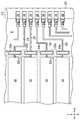
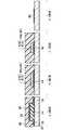
駆動基板5の構成を図2〜図4に示す。図2は、駆動基板5の概略平面図である。図3は、駆動基板5におけるスイッチ電極12と外部接続端子16との接続構造を一部拡大して概略的に示す平面図である。図4は、図中左側から順に図3のA−A線、B−B線、C−C線、D−D線における断面構造を示す断面図である。<Configuration of
The structure of the
駆動基板5は、図2に示すように、ベース基板であるガラス基板などの絶縁性基板10上に、視差バリア領域Bにストライプ状に配列された複数の駆動スイッチ電極12と、該各駆動スイッチ電極12に電気的に接続されて当該スイッチ電極12毎に額縁領域Fを視差バリア領域B側から駆動端子領域DT側に引き出された引出配線14と、該各引出配線14の引き出し先に当該配線14毎に設けられた外部接続端子16とを備えている。 As shown in FIG. 2, the
駆動スイッチ電極12は、各々図2で上下方向(Y軸方向;例えば画面縦方向)に線状に延びる細長い略長方形状に形成され、図2で左右方向(X軸方向;例えば画面横方向)に所定の間隔をあけて配置されており、当該スイッチ電極12同士の間に隙間が形成されている。各駆動スイッチ電極12の一端側には、図3に示すように、当該スイッチ電極12から配線12aが引き出されると共に、その先端に内部接続端子12bが形成されている。これら各駆動スイッチ電極12は、透明導電性酸化物であるITO又はIZOからなり、本発明の透明電極を構成している。 The
外部接続端子16は、絶縁性基板10の端縁に沿って互いに所定の間隔をあけて一列に並んでいる。これら各外部接続端子16は、透明導電性酸化物であるITO又はIZOからなり、上記駆動スイッチ電極12と同一膜から形成されている。 The
引出配線14は、視差バリア領域Bの周辺から駆動端子領域DTの手前まで互いに並んで延びている。各引出配線14は、内部接続端子12bに引き出し基端部14aを重ねて接続されていると共に、外部接続端子16に引き出し先端部14bを重ねて接続されている。これら各引出配線14は、図4(B−B断面及びC−C断面)に示すように、バリア金属層15A及び低抵抗金属層15Bが順に積層されて構成されている。 The
バリア金属層15Aは、内部接続端子12b及び外部接続端子16との接触部を構成している。このバリア金属層15Aは、高融点金属窒化物である窒化チタン(TiN)からなり、その窒素濃度が35atoms/cm2以上且つ65atoms/cm2以下であって、比抵抗が150μΩcm以上且つ500μΩcm以下の範囲にある。低抵抗金属層15Bは、窒化チタン(TiN)よりも低抵抗なチタン(Ti)からなり、比抵抗が60μΩcm以上且つ75μΩcm以下の範囲にある。The barrier metal layer 15 </ b> A constitutes a contact portion between the
このように引出配線14における内部接続端子12b及び外部接続端子16との接触部が、窒素濃度35atoms/cm2〜65atoms/cm2の窒化チタン(TiN)で形成されていることによって、当該引出配線14が両接続端子12b,16から剥がれることを防止できる。In this way, the contact portion between the
すなわち、引出配線14における内部接続端子12b及び外部接続端子16との接触部を窒化チタン(Ti)により形成すると、当該引出配線14と両接続端子12b,16との相互の酸化還元反応を抑える効果が得られる。ここで、仮に、当該引出配線14の接触部における窒素濃度が35atoms/cm2未満であると、当該引出配線14と接続端子12b,16との相互の酸化還元反応を引出配線14の剥がれを防止するにまで十分に抑えられない。他方、仮に、上記引出配線14の接触部における窒素濃度が65atoms/cm2よりも高いと、当該引出配線14を形成するための成膜時に、成膜装置内に堆積する膜が剥がれやすく、それがパーティクル源となって、基板表面に多量のパーティクルが付着したり、その成膜した膜内にパーティクルが混入する不具合を招き、その上、窒化チタン(TiN)は窒素濃度に応じてその比抵抗が高くなるため、配線抵抗が高くなり過ぎて引出配線14が機能しなくなるおそれもある。That is, when the contact portion between the
これに対して、本実施形態では、引出配線14における内部接続端子12b及び外部接続端子16との接触部を構成するバリア金属層15Aの窒素濃度が35atoms/cm2以上であるので、当該引出配線14と両接続端子12b,16との相互の酸化還元反応を十分に抑えることができる。そして、バリア金属層15Aにおける窒素濃度が65atoms/cm2以下であるので、当該引出配線14を形成するための成膜時のパーティクル発生が抑制されて、基板表面へのパーティクル付着及び成膜した膜内へのパーティクル混入を防止することができる。しかも、バリア金属層15Aの比抵抗を配線として必要な導電性を確保できる範囲に抑えることができる。さらに、このバリア金属層15A上には低抵抗金属層15Bが積層されているので、当該引出配線14を窒化チタン(TiN)のみからなる場合に比べて低抵抗化することができ、駆動基板5における引出配線14に必要な導電性を得ることができる。また、窒化チタン(TiN)の結晶構造は、立方晶系の構造であって、ITOやIZOなどの透明導電性酸化物と結晶系が同じであるので、引出配線14の形成時に当該配線14に残留する膜ストレスを緩和することができる。したがって、引出配線14が内部接続端子12b及び外部接続端子16から剥がれることを防止できる。On the other hand, in the present embodiment, the nitrogen concentration of the
上記バリア金属層15Aの窒素濃度は、上述の如く当該バリア金属層15Aと接続端子12b,16との酸化還元反応を抑制する観点から、35atoms/cm2以上且つ65atoms/cm2以下であることが好ましく、さらに、40atoms/cm2以上且つ50atoms/cm2以下であることがよりいっそう好ましい。The nitrogen concentration of the
なお、本実施形態では、バリア金属層15Aが窒化チタン(TiN)からなるとしているが、当該バリア金属層15Aは、窒化チタン(TiN)に代えて、窒化モリブデン(MoN)、窒化タンタル(TaN)、窒化タングステン(WN)又は窒化クロム(CrN)により形成されていてもよく、その他の高融点金属によって形成されていても構わない。また、低抵抗金属層15Bも、チタン(Ti)に限らず、これに代えて、モリブデン(Mo)、タンタル(Ta)、タングステン(W)又はクロム(Cr)により形成されていてもよく、その他の高融点金属によって形成されていても構わない。 In this embodiment, the
<コモン基板6の構成>
コモン基板6の構成を図5及び図6に示す。図5は、コモン基板6の概略平面図である。図6は、コモン基板6におけるスイッチ電極22と外部接続端子26との接続構造を一部拡大して概略的に示す平面図である。<Configuration of
The configuration of the
コモン基板6は、図5に示すように、ベース基板であるガラス基板などの絶縁性基板20上に、視差バリア領域Bにストライプ状に配列された複数のコモンスイッチ電極22と、該各コモンスイッチ電極22に電気的に接続されて当該スイッチ電極22毎に額縁領域Fを視差バリア領域B側からコモン端子領域CT側に引き出された引出配線24と、該各引出配線24の引き出し先に当該配線24毎に設けられた外部接続端子26とを備えている。 As shown in FIG. 5, the
コモンスイッチ電極22は、各々上記駆動スイッチ電極12と交差するように各々X軸方向に線状に延びる細長い略長方形状に形成され、Y軸方向に所定の間隔をあけて配置されており、当該スイッチ電極22同士の間に隙間が形成されている。各コモンスイッチ電極22の一端側には、図6に示すように、当該スイッチ電極22から配線22aが引き出されると共に、その先端に内部接続端子22bが形成されている。これら各コモンスイッチ電極22も、透明導電性酸化物であるITO又はIZOからなり、本発明の透明電極を構成している。 Each of the
外部接続端子26は、絶縁性基板20の外縁に沿って互いに所定の間隔をあけて一列に並んでいる。これら各外部接続端子26は、透明導電性酸化物であるITO又はIZOからなり、上記コモンスイッチ電極22と同一膜から形成されている。 The
引出配線24は、視差バリア領域Bの周辺からコモン端子領域CTの手前まで互いに並んで延びている。各引出配線24は、内部接続端子22bに引き出し基端部24aを重ねて接続されていると共に、外部接続端子26に引き出し先端部24bを重ねて接続されている。 The
これら各引出配線24は、駆動基板5側の引出配線14と同様に、窒素濃度が35atoms/cm2以上且つ65atoms/cm2以下(好ましくは40atoms/cm2以上且つ50atoms/cm2以下)の窒化チタン(TiN)からなるバリア金属層と、チタン(Ti)からなる低抵抗金属層とが順に積層されて構成されている。これにより、コモン基板6においても、引出配線24と内部接続端子22b及び外部接続端子26との間で駆動基板5と同様な作用が奏され、当該引出配線24が両接続端子22b,26から剥がれることを防止できる。Each of the lead lines 24 is nitrided with a nitrogen concentration of 35 atoms / cm2 or more and 65 atoms / cm2 or less (preferably 40 atoms / cm2 or more and 50 atoms / cm2 or less), similarly to the lead lines 14 on the
なお、本実施形態では、引出配線24のバリア金属層が窒化チタン(TiN)からなるとしているが、当該バリア金属層は、窒化チタン(TiN)に代えて、窒化モリブデン(MoN)、窒化タンタル(TaN)、窒化タングステン(WN)又は窒化クロム(CrN)により形成されていてもよく、その他の高融点金属によって形成されていても構わない。また、引出配線24の低抵抗金属層も、チタン(Ti)に限らず、これに代えて、モリブデン(Mo)、タンタル(Ta)、タングステン(W)又はクロム(Cr)により形成されていてもよく、その他の高融点金属によって形成されていても構わない。 In this embodiment, the barrier metal layer of the lead-
これら駆動基板5及びコモン基板6は、例えば矩形状に形成され、互いに対向する内側表面に配向膜(不図示)がそれぞれ設けられている。さらにコモン基板6の外側表面には第3偏光板H3が設けられている。このコモン基板6上の第3偏光板H3は、上記対向基板2上の第2偏光板H2と透過軸の方向が同じである。液晶層8は、例えば電気光学特性を有するネマチックの液晶材料などにより構成されている。 The
<2D/3D切替型の液晶表示装置S1の作動>
上記構成の液晶表示装置S1では、通常の2D表示を行う第1の表示状態である2D表示状態と、観察者の左右それぞれの目に異なる視点から見た像を視認させることにより視差を与えて3D表示を行う第2の表示状態である3D表示状態とのいずれかの表示状態で画像表示が行われる。<Operation of 2D / 3D Switching Type Liquid Crystal Display S1>
In the liquid crystal display device S1 having the above-described configuration, a parallax is given by visually recognizing a 2D display state, which is a first display state for performing normal 2D display, and an image viewed from different viewpoints on the left and right eyes of the observer. Image display is performed in any one of the display states of the 3D display state, which is the second display state in which 3D display is performed.
表示動作時の液晶表示パネルDPでは、ゲート信号が各ゲート配線に順に出力されてゲート配線が駆動され、駆動された同一のゲート配線に接続されているTFTが一斉にオン状態となったときに、ソース配線を介してソース信号がオン状態の各TFTに送られ、それら各TFTを介して画素電極に所定の電荷が書き込まれる。このような画素電極への選択的な電荷の書き込み動作が線順次で表示領域Dをなす画素の全行に対して実施される。これにより、TFT基板1の各画素電極と対向基板2の共通電極との間において電位差が生じ、液晶層4に所定の電圧が印加される。そして、液晶表示パネルDPでは、液晶層4に印加する電圧の大きさによって液晶分子の配向状態を変えることにより、液晶層4でのバックライトユニットBLからの光の透過率を調整して画像が表示される。 In the liquid crystal display panel DP at the time of display operation, when gate signals are sequentially output to the respective gate lines to drive the gate lines, and the TFTs connected to the same driven gate lines are turned on all at once. The source signal is sent to each TFT in the on state via the source wiring, and a predetermined charge is written to the pixel electrode via each TFT. Such a selective charge writing operation to the pixel electrodes is performed on all the rows of pixels forming the display region D in a line sequential manner. Thereby, a potential difference is generated between each pixel electrode of the
3D表示状態での表示動作時には、液晶表示パネルDPにおいて、右目用画像と左目用画像とが各々画面横方向に複数列に分割されて互いの列が交互に並ぶように混合された複合画像が表示される。 During the display operation in the 3D display state, the liquid crystal display panel DP has a composite image in which the right-eye image and the left-eye image are each divided into a plurality of columns in the horizontal direction of the screen and the columns are alternately arranged. Is displayed.
そして、3D表示状態でのスイッチング液晶パネルSPでは、その駆動をオン状態とし、各駆動スイッチ電極12と各コモンスイッチ電極22とに異なる電位が一斉に印加される。このとき、各駆動スイッチ電極12と各コモンスイッチ電極22との間に所定の電圧が印加され、これら各駆動スイッチ電極12と各コモンスイッチ電極22とが重なる領域を通過した光の偏光軸がこれら両スイッチ電極12,22が重なる領域間を通過した光の偏光軸に対して90°変えられる。これにより、各駆動スイッチ電極12と各コモンスイッチ電極22とが重なる領域と通過した光は、その偏光軸が第3偏光板H3の透過軸と90°の角度をなすので、第3偏光板H3を透過しない。一方、これら両スイッチ電極12,22が重なる領域間を通過した光は、その偏光軸が第3偏光板H3の透過軸と平行であるので、第3偏光板H3を透過する。 In the switching liquid crystal panel SP in the 3D display state, the driving is turned on, and different potentials are applied to the driving
本実施形態では、スイッチング液晶パネルSPと第3偏光板H3との関連した光学作用によって、スイッチング液晶パネルSPにおける駆動スイッチ電極12とコモンスイッチ電極22とが重なる各領域が遮光部を、これら両スイッチ電極間の各領域が透光部となり、視差バリア領域において、格子状の透光部と該透光部の格子間にマトリクス状に配置された遮光部とを有する視差バリアとしての機能が有効に発揮される。つまり、スイッチング液晶パネルSP及び第3偏光板H3が本発明の視差バリアを構成している。 In the present embodiment, due to the optical action related to the switching liquid crystal panel SP and the third polarizing plate H3, each region where the
上記液晶表示パネルDPに表示された右目用画像と左目用画像との複合画像は、上記スイッチング液晶パネルSP及び第3偏光板H3がなす視差バリアを介することで、観察者の左右それぞれの目に異なる視点から見た画像が視認されるように右目用画像と左目用画像とで異なる所定の視野角に分離されて、3D表示が行われる。このとき、表示画面を90°回転させて縦と横とを切り替えても、視差バリアがマトリクス状に配置された遮光部を有しているので、液晶表示パネルDPに表示された複合画像も同方向に90°回転させて表示することにより、当該複合画像の右目用画像と左目用画像とをそれぞれ所定の視野角に分離することができ、所望の3D表示を実現することができる。本実施形態では、液晶表示パネルDPにおいて、右目用画像に対応する画素により構成される領域及び左目用画像に対応する画素により構成される領域のそれぞれが第1の表示領域及び第2の表示領域となる。 The composite image of the image for the right eye and the image for the left eye displayed on the liquid crystal display panel DP is passed through the parallax barrier formed by the switching liquid crystal panel SP and the third polarizing plate H3, so that the left and right eyes of the observer The right-eye image and the left-eye image are separated into different predetermined viewing angles so that images viewed from different viewpoints are visually recognized, and 3D display is performed. At this time, even if the display screen is rotated 90 ° to switch between portrait and landscape, the composite image displayed on the liquid crystal display panel DP is the same because the parallax barrier has the light-shielding portion arranged in a matrix. By rotating and displaying 90 degrees in the direction, the right-eye image and the left-eye image of the composite image can be separated into predetermined viewing angles, and a desired 3D display can be realized. In the present embodiment, in the liquid crystal display panel DP, the first display region and the second display region are the region formed by the pixels corresponding to the right-eye image and the region formed by the pixels corresponding to the left-eye image, respectively. It becomes.
一方、2D表示状態による表示動作時には、液晶表示パネルDPにおいて、通常の2次元平面画像が表示される。そして、スイッチング液晶パネルSPでは、その駆動をオフ状態とし、各駆動スイッチ電極12と各コモンスイッチ電極22とに同じ電位が印加されることにより、視差バリアとしての機能を無効にして、入射した光をそのままの偏光軸として出射させる。これにより、観察者の両目に同じ画像が視認されて、2D表示が行われる。 On the other hand, during the display operation in the 2D display state, a normal two-dimensional planar image is displayed on the liquid crystal display panel DP. In the switching liquid crystal panel SP, the drive is turned off, and the same potential is applied to each
−製造方法−
次に、上記2D/3D切替型の液晶表示装置S1の製造方法について、一例を挙げて説明する。本実施形態では、駆動基板5とコモン基板6とを一枚ずつ製造し、それら両基板5,6を貼り合わせて一枚のスイッチング液晶パネルSPを製造する枚葉方式の製造方法を例に挙げて説明するが、複数のセル単位を含むマザーパネルを作製し、該マザーパネルをセル単位毎に分断することにより、複数のスイッチング液晶パネルSPを同時に作製する多面取り方式の製造方法にも適用することができる。このことは液晶表示パネルDPについても同様である。-Manufacturing method-
Next, a manufacturing method of the 2D / 3D switching type liquid crystal display device S1 will be described with an example. In the present embodiment, a single-wafer manufacturing method in which the
2D/3D切替型の液晶表示装置S1の製造方法は、スイッチング液晶パネル製造工程と、液晶表示パネル製造工程と、バックライトユニット製造工程と、モジュール化工程とを含む。 The manufacturing method of the 2D / 3D switching type liquid crystal display device S1 includes a switching liquid crystal panel manufacturing process, a liquid crystal display panel manufacturing process, a backlight unit manufacturing process, and a modularization process.
<スイッチング液晶パネル製造工程>
スイッチング液晶パネル製造工程は、駆動基板製造工程と、コモン基板製造工程と、貼合工程とを含む。<Switching LCD panel manufacturing process>
The switching liquid crystal panel manufacturing process includes a drive board manufacturing process, a common board manufacturing process, and a bonding process.
<駆動基板製造工程>
駆動基板製造工程を図7(a)〜(c)に示す。なお、この図7(a)〜(c)は、図4対応箇所の断面をそれぞれ示している。<Drive substrate manufacturing process>
The drive substrate manufacturing process is shown in FIGS. 7A to 7C show cross sections corresponding to FIG.
まず、予め準備したガラス基板などの絶縁性基板10上に、スパッタリング法により、立方晶系のビックスバイト型構造を有するITO又はIZOからなる透明導電膜を成膜する。そして、この透明導電膜をフォトリソグラフィーによりパターニングして、図7(a)に示すように、駆動スイッチ電極12及び外部接続端子16を形成する。 First, a transparent conductive film made of ITO or IZO having a cubic bixbyite structure is formed on an insulating
次いで、駆動スイッチ電極12及び外部接続端子16が形成された基板上に、スパッタリング法により、図7(b)に示すように、立方晶系の塩化ナトリウム(NaCl)型構造を有する窒化チタン(TiN)膜60と六方晶系の結晶構造を有するチタン(Ti)膜62とを順に成膜して、これらが積層された金属積層膜64を形成する。そして、この金属積層膜64をフォトリソグラフィーによりパターニングして、図7(c)に示すように、引出配線14を形成する。 Next, on the substrate on which the
このようにして、駆動基板5を製造することができる。 In this way, the
<コモン基板製造工程>
予め準備したガラス基板などの絶縁性基板20上に、上記駆動基板製造工程と同様にして、コモンスイッチ電極22、引出配線24及び外部接続端子26をフォトリソグラフィーを繰り返し行って形成することにより、コモン基板6を製造する。<Common substrate manufacturing process>
The
<貼合工程>
駆動基板5及びコモン基板6の表面に対して、印刷法などにより配向膜をそれぞれ形成した後に、必要に応じてラビング処理を行う。次いで、駆動基板5又はコモン基板6の表面に対して、ディスペンサなどにより紫外線硬化型の樹脂からなるシール材7を枠状に描画し、該シール材7の内側領域に液晶材料を所定量滴下する。<Bonding process>
An alignment film is formed on the surfaces of the
そして、駆動基板5とコモン基板6とをシール材7及び液晶材料を介して減圧下で貼り合わせて液晶層8を構成した後、その貼り合わせた貼合体を大気圧下に開放することにより、貼合体の表面を加圧する。さらに、その状態でシール材7を紫外線の照射によって硬化させることにより、駆動基板5とコモン基板6とを接着してスイッチング液晶パネルSPを製造する。しかる後に、駆動基板5の外側表面に対して第3偏光板H3を貼り付ける。 Then, after the
<液晶表示パネル製造工程>
液晶表示パネル製造工程は、TFT基板製造工程と、対向基板製造工程と、貼合工程とを含む。<Liquid crystal display panel manufacturing process>
The liquid crystal display panel manufacturing process includes a TFT substrate manufacturing process, a counter substrate manufacturing process, and a bonding process.
<TFT基板製造工程>
予め準備したガラス基板などの絶縁性基板上に、ゲート配線、ソース配線、TFT及び画素電極を、フォトリソグラフィーを繰り返し行う周知の方法で形成することにより、TFT基板1を製造する。<TFT substrate manufacturing process>
A
<対向基板製造工程>
予め準備したガラス基板などの絶縁性基板上に、ブラックマトリクス、カラーフィルタ、共通電極及びフォトスペーサを、フォトリソグラフィーを繰り返し行う周知の方法で形成することにより、対向基板2を製造する。<Opposite substrate manufacturing process>
The
<貼合工程>
TFT基板1及び対向基板2の表面に対して配向膜を形成した後、必要に応じてラビング処理を行う。そして、スイッチング液晶パネル製造工程における貼合工程と同様にして、TFT基板1と対向基板2とを貼り合わせて液晶層4を構成し、シール材3を硬化させてこれら両基板1,2を接着することにより、液晶表示パネルDPを製造する。しかる後、TFT基板1及び対向基板2の外側表面に対して、第1偏光板H1及び第2偏光板H2をそれぞれ貼り付ける。<Bonding process>
After the alignment film is formed on the surfaces of the
<バックライトユニット製造工程>
まず、公知の射出成形装置などを用いて導光板のベースとなるアクリル樹脂板を成形し、該アクリル樹脂板に光を散乱させるための例えばドット形状のパターンを形成することにより、導光板を製造する。次いで、この導光板に反射シートや拡散シート、プリズムシートなどの光学シートを貼り付けて組み立てる。その後、導光板と光学シートとの貼合体にLEDや冷陰極管などの光源を取り付けることにより、バックライトユニットBLを製造する。<Backlight unit manufacturing process>
First, an acrylic resin plate as a base of the light guide plate is formed using a known injection molding apparatus, and a light guide plate is manufactured by, for example, forming a dot-shaped pattern for scattering light on the acrylic resin plate. To do. Next, an optical sheet such as a reflection sheet, a diffusion sheet, or a prism sheet is attached to the light guide plate and assembled. Then, the backlight unit BL is manufactured by attaching a light source such as an LED or a cold cathode tube to the bonded body of the light guide plate and the optical sheet.
<モジュール化工程>
スイッチング液晶パネルSP及び液晶表示パネルDPの各端子領域DT,CTに対し、異方性導電膜を介してFPCなどの配線基板をそれぞれ実装する。そして、スイッチング液晶パネルSPと液晶表示パネルDPとを両面テープなどの貼付材9を介して貼り合わせ、液晶表示パネルDPの背面側にバックライトユニットBLを搭載する。このようにして、スイッチング液晶パネルSP、液晶表示パネルDP及びバックライトユニットBLをモジュール化する。<Modularization process>
A wiring board such as FPC is mounted on each terminal region DT, CT of the switching liquid crystal panel SP and the liquid crystal display panel DP via an anisotropic conductive film. Then, the switching liquid crystal panel SP and the liquid crystal display panel DP are bonded to each other through an adhesive material 9 such as a double-sided tape, and the backlight unit BL is mounted on the back side of the liquid crystal display panel DP. In this way, the switching liquid crystal panel SP, the liquid crystal display panel DP, and the backlight unit BL are modularized.
以上の工程を行って、図1に示す2D/3D切替型の液晶表示装置S1を製造することができる。 By performing the above steps, the 2D / 3D switching type liquid crystal display device S1 shown in FIG. 1 can be manufactured.
−実施形態1の効果−
この実施形態1によると、駆動基板5上の引出配線14における内部接続端子12b及び外部接続端子16との接触部を構成するバリア金属層15Aが窒化チタン(TiN)により形成され、その窒素濃度が35atoms/cm2以上且つ65atoms/cm2以下であるので、当該引出配線14が両接続端子12b,16から剥がれることを防止でき、これら引出配線14と両接続端子12b,16とを確実に接続して駆動基板5を不良なく正常に動作させることができる。-Effect of Embodiment 1-
According to the first embodiment, the
また、コモン基板6上の引出配線24も上記駆動基板5上の引出配線14と同様な構成を備えるので、当該引出配線24が内部接続端子22b及び外部接続端子26から剥がれることを防止でき、これら引出配線24と両接続端子22b,26とを確実に接続してコモン基板6も不良なく正常に動作させることができる。 Further, since the lead-
したがって、スイッチング液晶パネルSP及びこれを備える2D/3D切替型の液晶表示装置S1について、歩留りの低下及び製造コストの増大を改善することができ、低コスト化することができる。 Therefore, with respect to the switching liquid crystal panel SP and the 2D / 3D switching type liquid crystal display device S1 including the switching liquid crystal panel SP, it is possible to improve yield reduction and increase in manufacturing cost, and to reduce costs.
《実施形態1の変形例》
図8は、上記実施形態1の変形例に係る引出配線14の構造を示す断面図であって、図中左側から順に図4のB−B線及びC−C線における断面相当箇所を示している。<< Modification of
FIG. 8 is a cross-sectional view showing the structure of the lead-
上記実施形態1では、引出配線14が窒化チタン(TiN)からなるバリア金属層15Aとチタン(Ti)からなる低抵抗金属層14Bとが順に積層された2層構造(Ti/TiN)を有するとしたが、本変形例の引出配線14は、窒化チタン(TiN)からなるバリア金属層15Aと、チタン(Ti)からなる低抵抗金属層15Bと、窒化チタン(TiN)からなる窒化金属層15Cとが順に積層された3層構造(TiN/Ti/TiN)を有している。 In
このような積層構造の引出配線14を備える駆動基板5は、駆動スイッチ電極12及び外部接続端子16を形成した基板上に、スパッタリング法により、窒化チタン(TiN)膜60及びチタン(Ti)膜62の成膜に続いて、さらに窒化チタン(TiN)膜を成膜して、3層構造の金属積層膜を形成し、該金属積層膜をフォトリソグラフィーによりパターニングして、引出配線14を形成することにより、製造することができる。 The
なお、この変形例では駆動基板5の引出配線14の構造について説明したが、同様な構造をコモン基板6の引出配線24にも採用することができる。 In this modification, the structure of the
《発明の実施形態2》
この実施形態2では、本発明をタッチパネルに適用した場合について、表示装置の一例として液晶表示装置を挙げて、タッチパネルTP付きの液晶表示装置S2について説明する。<<
In the second embodiment, when the present invention is applied to a touch panel, a liquid crystal display device S2 with a touch panel TP will be described by taking a liquid crystal display device as an example of a display device.
−タッチパネルTP付きの液晶表示装置S2の構成−
タッチパネルTP付きの液晶表示装置S2の断面構造を図9に示す。-Configuration of liquid crystal display device S2 with touch panel TP-
FIG. 9 shows a cross-sectional structure of the liquid crystal display device S2 with the touch panel TP.
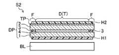
タッチパネルTP付きの液晶表示装置S2は、透過型液晶表示装置であって、上記実施形態1と同様な構成の液晶表示パネルDP及びバックライトユニットBLと、液晶表示パネルDPの表面側に設けられた電極基板であるタッチパネルTPとを備えている。 The liquid crystal display device S2 with the touch panel TP is a transmissive liquid crystal display device, and is provided on the surface side of the liquid crystal display panel DP and the backlight unit BL having the same configuration as in the first embodiment and the liquid crystal display panel DP. And a touch panel TP which is an electrode substrate.
<タッチパネルTPの構成>
タッチパネルTPの構成を図10〜図12に示す。図10は、タッチパネルTPの概略平面図である。図11は、タッチパネルTPにおけるタッチ位置検出用の電極22と外部接続端子48との接続構造を一部拡大して示す平面図である。図12は、図中左側から順に図11のA−A線、B−B線、C−C線、D−D線における断面構造を示す断面図である。<Configuration of touch panel TP>
The configuration of the touch panel TP is shown in FIGS. FIG. 10 is a schematic plan view of the touch panel TP. FIG. 11 is a partially enlarged plan view showing a connection structure between the touch
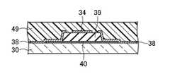
本実施形態のタッチパネルTPは、液晶表示パネルDPの対向基板2を構成する絶縁性基板30の表面に直接形成され、タッチパネルTP付きの液晶表示装置S2を全体として薄型に構成している。タッチパネルTPは、投影型静電容量方式(プロジェクテッドキャパシティブ方式)のタッチパネルに構成され、図10に示すように、接触体(使用者の指など)により接触されたタッチ位置を検出するための領域である例えば矩形状のタッチ領域Tと、該タッチ領域Tの周囲に設けられた例えば矩形枠状の額縁領域Fと、該額縁領域Fの一辺側(図10で右側)に設けられた端子領域TTとを有している。タッチ領域Tは、液晶表示パネルDPの表示領域Dに対応する領域に配置されている。額縁領域Fは、液晶表示パネルDPの非表示領域に対応する領域に配置されている。 The touch panel TP of the present embodiment is directly formed on the surface of the insulating
そして、タッチパネルTPは、タッチ領域Tに設けられたタッチ位置検出用のタッチ検出電極32,38と、該タッチ検出電極32,38に電気的に接続されて額縁領域Fをタッチ領域T側から端子領域TT側に引き出された複数の引出配線46と、これら各引出配線46の引き出し先に設けられた外部接続端子48と、これら各外部接続端子46に電気的に接続された外部回路であるコントローラ50とを備えている。 The touch panel TP includes
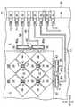
タッチ検出電極32,38は、マトリクス状に配置された複数の第1電極32(図10で斜線を付した電極)と、同じくマトリクス状に配置された複数の第2電極38(図10で白抜きの電極)とにより構成されている。これら第1電極32及び第2電極38は、図10で斜め方向に交互に並ぶように全体としてハニカム状に配列されている。 The
第1電極32は、略矩形状に形成され、図10で左右方向(X軸方向)及び上下方向(Y軸方向)に互いの角部を突き合わせるように所定の間隔で配置されている。そして、X軸方向に整列する複数の第1電極32は、図11に示すように、隣り合う第1電極32同士が第1連結部34により連結されて一体に形成され、第1電極群36を構成している。つまり、第1電極32及び第1連結部34は、X軸方向に交互に配置されており、この第1連結部34を介して一体に形成された第1電極32の列からなる第1電極群36が、Y軸方向に互いに平行に複数列並んでいる。第1電極32及び第1連結部34は、透明導電性酸化物であるITO又はIZOからなる。 The
第2電極38も、例えば略矩形状に形成され、X軸方向及びY軸方向に互いの角部を突き合わせるように所定の間隔で配置されている。そして、Y軸方向に整列する複数の第2電極38は、隣り合う第2電極38同士が第2連結部40により連結されて電気的に接続され、第2電極群42を構成している。つまり、第2電極38及び第2連結部40は、Y軸方向に交互に配置されており、この第2連結部40を介して電気的に接続された第2電極38の列からなる第2電極群42が、X軸方向に互いに平行に複数列並んでいる。第2電極38及び第2連結部40も、透明導電性酸化物であるITO又はIZOからなる。 The
上記第1電極群36(第1電極32)、第1連結部34及び第2電極群42(第2電極38)は、図12(A−A断面)に示すように、対向基板2を構成する絶縁性基板30の外側表面に形成されている。そして、第1連結部34だけが島状の層間絶縁膜39によって覆われている。一方、第2連結部40は、層間絶縁膜39上を第1連結部34と交差する方向に延びて、該層間絶縁膜39を介して第1連結部34を跨ぐ架橋構造を構成しており、その両端部が隣り合う第2電極38の角部に接続されている。 The first electrode group 36 (first electrode 32), the first connecting
このように本実施形態では、第1電極群36と第2電極群42とが同一層に設けられているので、タッチ位置における第1電極32及び第2電極38と指などの接触体との間に形成される静電容量の変化を同程度に生じさせることができる。これによって、第1電極32と第2電極38とで静電容量の変化の感度差を少なくすることができ、感度の良いタッチ位置の検出を行うことができる。 Thus, in this embodiment, since the
上記各第1電極群36及び各第2電極群42の一方側には、図11に示すように、第1電極32又は第2電極38から配線43が引き出されると共に、その先端に内部接続端子44が形成されている。本実施形態では、これら第1電極群36、第2電極群42、配線42及び内部接続端子44が本発明の透明電極を構成している。 As shown in FIG. 11, a
上記第1電極群36(第1電極32)、第2電極群42(第2電極38)、第2連結部40及び層間絶縁膜39は、図12(A−A断面)に示すように、保護絶縁膜49によって覆われている。この保護絶縁膜49は、アクリルベースの有機絶縁材料などからなり、図11に示すように端子領域TTには形成されておらず、各外部接続端子48を外部に露出させている。 The first electrode group 36 (first electrode 32), the second electrode group 42 (second electrode 38), the second connecting
外部接続端子48は、対向基板2を構成する絶縁性基板30の端縁に沿って互いに所定の間隔をあけて一列に並んでいる。これら各外部接続端子48は、透明導電性酸化物であるITO又はIZOからなり、上記第1電極32及び第2電極38と同一膜から形成されている。このように保護絶縁膜49の外部に露出する外部接続端子48は、ITO又はIZOからなるので、耐腐食性が高く、大気中においても腐食され難い。これにより、外部回路との接続において、当該接続端子48が腐食されることに起因して、その抵抗が高くなり接続不良を引き起こすことが回避される。 The
引出配線46は、タッチ領域Tの周辺から端子領域TTの手前まで互いに並んで延びている。これら各引出配線46は、保護絶縁膜49によって覆われており、その全体が当該絶縁膜49の外縁よりも内側に配置されている。これにより、保護絶縁膜49によって外部からの湿気等の進入が阻止されて、引出配線46の腐食が良好に防止される。 The lead wirings 46 extend side by side from the periphery of the touch area T to the front of the terminal area TT. Each of the lead wirings 46 is covered with a protective insulating
各引出配線46は、内部接続端子44に引き出し基端部46aを重ねて接続されていると共に、外部接続端子48に引き出し先端部46bを重ねて接続されている。これら各引出配線46は、図12(B−B断面及びC−C断面)に示すように、上記実施形態1における駆動基板5及びコモン基板6の引出配線14と同様に、窒素濃度が35atoms/cm2以上且つ65atoms/cm2以下(好ましくは40atoms/cm2以上且つ50atoms/cm2以下)の窒化チタン(TiN)からなるバリア金属層47Aと、チタン(Ti)からなる低抵抗金属層47Bとが順に積層されて構成されている。これにより、引出配線46と内部接続端子44及び外部接続端子48との間で上記実施形態1における駆動基板5と同様な作用が奏され、当該引出配線46が両接続端子44,48から剥がれることを防止できる。Each lead-
なお、本実施形態では、バリア金属層47Aが窒化チタン(TiN)からなるとしているが、当該バリア金属層47Aは、窒化チタン(TiN)に代えて、窒化モリブデン(MoN)、窒化タンタル(TaN)、窒化タングステン(WN)又は窒化クロム(CrN)により形成されていてもよく、その他の高融点金属によって形成されていても構わない。また、低抵抗金属層47Bも、チタン(Ti)に限らず、これに代えて、モリブデン(Mo)、タンタル(Ta)、タングステン(W)又はクロム(Cr)により形成されていてもよく、その他の高融点金属によって形成されていても構わない。 In this embodiment, the
<コントローラ50の構成>
コントローラ50は、例えばTAB(Tape Automated Bonding)と呼ばれる駆動集積回路として端子領域TTに実装されている。このコントローラ50は、検出回路52として、タッチ領域Tが接触体にタッチされることにより、タッチ位置にある第1電極32及び第2電極38と接触体との間に生じる静電容量の変化を検出する静電容量検出回路、或いは、タッチされることによりタッチ位置にある第1電極32及び第2電極38のそれぞれに生じるインピーダンスの変化を検出するインピーダンス検出回路を備えている。そして、コントローラ50は、引出配線46を経由して検出回路52により検出される信号同士を比較することにより、タッチ領域Tにおける接触体のタッチ位置、及びそのタッチ位置の移動動作を検出するように構成されている。<Configuration of
The
−製造方法−
次に、上記タッチパネルTP付きの液晶表示装置S2の製造方法について、一例を挙げて説明する。タッチパネルTP付きの液晶表示装置S2の製造方法は、タッチパネル製造工程と、液晶表示パネル製造工程と、バックライトユニット製造工程と、モジュール化工程とを含む。なお、液晶表示パネル製造工程及びバックライトユニット製造工程は、上記実施形態1と同様であるので、その詳細な説明を省略する。-Manufacturing method-
Next, a method for manufacturing the liquid crystal display device S2 with the touch panel TP will be described with an example. The manufacturing method of the liquid crystal display device S2 with the touch panel TP includes a touch panel manufacturing process, a liquid crystal display panel manufacturing process, a backlight unit manufacturing process, and a modularization process. In addition, since the liquid crystal display panel manufacturing process and the backlight unit manufacturing process are the same as those in the first embodiment, detailed description thereof is omitted.
<タッチパネル製造工程>
タッチパネル製造工程を図13及び図14に示す。図13は、タッチパネル製造工程の前半ステップを示す工程図である。図14は、タッチパネル製造工程の後半ステップを示す工程図である。なお、これら図13及び図14は、図12対応箇所の断面を示している。<Touch panel manufacturing process>
The touch panel manufacturing process is shown in FIGS. FIG. 13 is a process diagram showing the first half of the touch panel manufacturing process. FIG. 14 is a process diagram showing the latter half of the touch panel manufacturing process. Note that FIGS. 13 and 14 show cross sections corresponding to FIG.
まず、予め準備したガラス基板などの絶縁性基板30上に、スパッタリング法により、立方晶系のビックスバイト型構造を有するITO又はIZOからなる透明導電膜を成膜する。そして、この透明導電膜をフォトリソグラフィーによりパターニングして、図13(a)に示すように、第1電極群36(第1電極32)、第1連結部34、第2電極群42(第2電極38)及び外部接続端子48を形成する。 First, a transparent conductive film made of ITO or IZO having a cubic bixbyite structure is formed on an insulating
次いで、第1電極群36(第1電極32)、第1連結部34、第2電極群42(第2電極38)及び外部接続端子48が形成された基板上に、スパッタリング法により、図13(b)に示すように、立方晶系の塩化ナトリウム(NaCl)型構造を有する窒化チタン(TiN)膜60と六方晶系の結晶構造を有するチタン(Ti)膜62とを順に成膜して、これらが積層された金属積層膜64を形成する。そして、この金属積層膜64をフォトリソグラフィーによりパターニングして、図13(c)に示すように、引出配線46を形成する。 Next, on the substrate on which the first electrode group 36 (first electrode 32), the first connecting
続いて、引出配線46が形成された基板上に、CVD(Chemical Vapor Diposition)法により、第1電極群36(第1電極32)、第1連結部34、第2電極群42(第2電極38)、外部接続端子48及び引出配線46を覆うように、例えば窒化珪素(SiN)からなる絶縁膜を成膜する。そして、この絶縁膜をフォトリソグラフィーによりパターニングして、図14(a)に示すように、層間絶縁膜39を形成する。 Subsequently, the first electrode group 36 (first electrode 32), the first connecting
次に、層間絶縁膜39が形成された基板上に、スパッタリング法により、ITO又はIZOからなる透明導電膜を成膜する。そして、この透明導電膜をフォトリソグラフィーによりパターニングして、図14(b)に示すように、第2連結部40を形成する。 Next, a transparent conductive film made of ITO or IZO is formed on the substrate on which the
その後、第2連結部40が形成された基板上に、スピンコート法又はスリットコート法により、例えばアクリルベースの有機絶縁材料からなる絶縁膜を成膜する。そして、この絶縁膜をフォトリソグラフィーによりパターニングして、図14(c)に示すように、端子領域TTにある絶縁膜部分を除去して当該絶縁膜から外部接続端子48を露出させて、保護絶縁膜49を形成する。 After that, an insulating film made of, for example, an acrylic-based organic insulating material is formed on the substrate on which the
このようにして、タッチパネルTPを製造することができる。しかる後、このタッチパネル付きの基板30を対向基板製造工程に投入する。液晶表示パネル製造工程では、当該基板30の裏面側にブラックマトリクス及びカラーフィルタ等の構成を作り込んでタッチパネルTP付きの対向基板2を製造する他は、上記実施形態1と同様な工程を行う。 In this way, the touch panel TP can be manufactured. Thereafter, the
<モジュール化工程>
液晶表示パネルDPの端子領域に対し、異方性導電膜を介してFPCなどの配線基板を実装する。また、タッチパネルTPの端子領域TTに対してコントローラ50を実装する。そして、タッチパネルTP付きの液晶表示パネルDPの背面側にバックライトユニットBLを搭載する。このようにして、タッチパネルTP付きの液晶表示パネルDPとバックライトユニットBLとをモジュール化する。<Modularization process>
A wiring board such as FPC is mounted on the terminal region of the liquid crystal display panel DP through an anisotropic conductive film. In addition, the
以上の工程を行って、図9に示すタッチパネルTP付きの液晶表示装置S2を製造することができる。 The liquid crystal display device S2 with the touch panel TP shown in FIG. 9 can be manufactured by performing the above steps.
−実施形態2の効果−
この実施形態2によると、引出配線46における内部接続端子44及び外部接続端子48との接触部を構成するバリア金属層47Aが窒化チタン(TiN)により構成され、その窒素濃度が35atoms/cm2以上且つ65atoms/cm2以下であるので、引出配線46が両接続端子44,48から剥がれることを防止でき、これら引出配線46と両接続端子44,48とを確実に接続してタッチパネルTPを不良なく正常に動作させることができる。これにより、タッチパネルTP及びこれを備える液晶表示装置S2について、歩留りの低下及び製造コストの増大を改善することができ、低コスト化することができる。-Effect of Embodiment 2-
According to the second embodiment, the
《実施形態2の変形例》
図15は、上記実施形態2の変形例に係る引出配線46の構造を示す断面図であって、図中左側から順に図12のB−B線及びC−C線断面相当箇所を示している。<< Modification of
FIG. 15 is a cross-sectional view showing the structure of the lead-
上記実施形態2では、引出配線46が窒化チタン(TiN)からなるバリア金属層47Aとチタン(Ti)からなる低抵抗金属層47Bとが順に積層された2層構造(Ti/TiN)を有するとしたが、本変形例の引出配線46は、窒化チタン(TiN)からなるバリア金属層47Aと、チタン(Ti)からなる低抵抗金属層47Bと、窒化チタン(TiN)からなる窒化金属層47Cとが順に積層された3層構造(TiN/Ti/TiN)を有している。 In the second embodiment, the lead-
このような積層構造の引出配線46を備えるタッチパネルTPは、第1電極群36(第1電極32)、第1連結部34、第2電極群42(第2電極38)及び外部接続端子48を形成した基板上に、スパッタリング法により、窒化チタン(TiN)膜60及びチタン(Ti)膜62の成膜に続いて、さらに窒化チタン(TiN)膜を成膜して、3層構造の金属積層膜を形成し、該金属積層膜をフォトリソグラフィーによりパターニングして、引出配線46を形成することにより、製造することができる。 The touch panel TP including the
《その他の実施形態》
上記実施形態1,2及びこれらの変形例については、以下の構成及び製造方法としてもよい。<< Other Embodiments >>
About the said
<第1電極32、第1連結部34、第2電極38、第2連結部40の配置>
図16は、その他の実施形態に係るタッチパネルTPのタッチ領域Tを一部拡大して示す概略平面図である。図17は、図16のXVII−XVII線における断面構造を示す断面図である。<Arrangement of
FIG. 16 is a schematic plan view showing a partially enlarged touch region T of the touch panel TP according to another embodiment. 17 is a cross-sectional view showing a cross-sectional structure taken along line XVII-XVII in FIG.
上記実施形態2では、第1電極32、第1連結部34及び第2電極38が基板30表面に形成されて第1連結部34だけが層間絶縁膜39によって覆われており、第2連結部40が層間絶縁膜39を介して第1連結部34を跨ぐ架橋構造になっている構成について説明したが、これに限らない。 In the second embodiment, the
例えば、図16及び図17に示すように、第1電極32、第2電極38、第2連結部40が基板30表面に形成されて隣り合う第2電極38の角部がその間の第2連結部40に重ねて接続され、該第2連結部40の中央部分だけが層間絶縁膜39によって覆われており、第1連結部34が層間絶縁膜39を介して第2連結部40を跨ぐ架橋構造になっていてもよい。また、層間絶縁膜39がタッチ領域Tの略全域に設けられ、該層間絶縁膜39上に第1電極群36(第1電極32)及び第2電極群42(第2電極38)が配置されていても構わない。 For example, as shown in FIGS. 16 and 17, the
<2D/3D切替型の液晶表示装置の構成>
図18は、その他の実施形態における2D/3D切替型の液晶表示装置S3の断面構造を概略的に示す断面図である。<Configuration of 2D / 3D switching type liquid crystal display device>
FIG. 18 is a cross-sectional view schematically showing a cross-sectional structure of a 2D / 3D switching type liquid crystal display device S3 in another embodiment.
上記実施形態1では、タッチパネルTPを備えない2D/3D切替型の液晶表示装置S1について説明したが、本発明はこれに限らず、図18に示すように、2D/3D切替型の液晶表示装置S3は、タッチパネルTPを備えていてもよい。この場合にも、タッチパネルTPは、液晶表示装置S3を全体として薄型化する観点から、スイッチング液晶パネルSPを構成する基板(例えばコモン基板6)の表面に直接形成されていることが好ましい。 In the first embodiment, the 2D / 3D switching type liquid crystal display device S1 that does not include the touch panel TP has been described. However, the present invention is not limited to this, and as shown in FIG. 18, the 2D / 3D switching type liquid crystal display device. S3 may include a touch panel TP. Also in this case, the touch panel TP is preferably directly formed on the surface of the substrate (for example, the common substrate 6) constituting the switching liquid crystal panel SP from the viewpoint of reducing the thickness of the liquid crystal display device S3 as a whole.
このようなタッチパネルTP付きの2D/3D切替型の液晶表示装置S3においては、駆動基板5及びコモン基板6が上記実施形態1と同様に、タッチパネルTPが上記実施形態2と同様に構成されていることが好ましい。このように構成されていれば、駆動基板5、コモン基板6及びタッチパネルTPのそれぞれを、引出配線14,24,46と内部接続端子12b,22b,44及び外部接続端子16,26,48とを確実に接続して正常に動作させることができるので、タッチパネルTP付きの2D/3D切替型の液晶表示装置S3としての歩留りの低下及び製造コストの増大を大幅に改善することができる。 In such a 2D / 3D switching liquid crystal display device S3 with a touch panel TP, the
また、タッチパネルTP付きの2D/3D切替型の液晶表示装置S3においては、駆動基板5及びコモン基板6の少なくとも一方だけが上記実施形態1と同様な構成を有していてもよく、タッチパネルTPだけが上記実施形態2と同様な構成を有していても構わない。このような構成であっても、タッチパネルTP付きの2D/3D切替型の液晶表示装置S3の歩留りの低下及び製造コストの増大の改善に寄与する。 In the 2D / 3D switching type liquid crystal display device S3 with the touch panel TP, at least one of the
また、上記実施形態1では、液晶表示パネルDPの前面側にスイッチング液晶パネルSPが配置された構成の2D/3D切替型の液晶表示装置S1について説明したが、本発明はこれに限らない。例えば、液晶表示パネルDPの背面側にスイッチング液晶パネルSPが配置された構成の2D/3D切替型の液晶表示装置であってもよい。 In the first embodiment, the 2D / 3D switching type liquid crystal display device S1 having the configuration in which the switching liquid crystal panel SP is disposed on the front side of the liquid crystal display panel DP has been described. However, the present invention is not limited to this. For example, a 2D / 3D switching type liquid crystal display device in which a switching liquid crystal panel SP is disposed on the back side of the liquid crystal display panel DP may be used.
またその他に、上記実施形態1では、2D/3D切替型の液晶表示装置S1を例に挙げて説明したが、本発明はこれに限らず、第2の表示状態において異なる視野角に分離される画像は、右目用画像及び左目用画像のように相互に関連を必要とするものだけではない。 In addition, in the first embodiment, the 2D / 3D switching type liquid crystal display device S1 has been described as an example. However, the present invention is not limited thereto, and the viewing angle is separated into different viewing angles in the second display state. Images are not only those that need to be related to each other, such as right-eye images and left-eye images.
例えば、自動車の運転席のドライバーにカーナビゲーションシステムの映像を表示し、且つ助手席の同乗者にテレビの映像を表示するような表示装置への利用が考えられる。複数の観察者に異なる映像を表示する場合には、視差バリアを介して視認される液晶表示パネルDPの画像が、所定の距離をおいた複数の観察者のそれぞれが観察すべき画像として分離できるように、視差バリアの遮光部と透光部の配置パターン、すなわち駆動スイッチ電極12及びコモンスイッチ電極22の配置パターンを適宜設定すればよい。 For example, it may be used for a display device that displays an image of a car navigation system on a driver in a driver's seat of a car and displays a television image on a passenger in a passenger seat. When displaying different images to a plurality of observers, the image of the liquid crystal display panel DP viewed through the parallax barrier can be separated as an image to be observed by each of the plurality of observers at a predetermined distance. As described above, the arrangement pattern of the light shielding part and the light transmitting part of the parallax barrier, that is, the arrangement pattern of the
また、本発明に係るスイッチング液晶パネルDPやタッチパネルTPなどの付加機能デバイスは、液晶表示装置S1,S2,S3だけでなく、有機EL(Electro Luminescence)表示装置や無機EL表示装置、プラズマ表示装置、FPD(Field Emission Display;電界放出ディスプレイ)などの他の各種表示装置にも適用することができる。 Further, the additional function devices such as the switching liquid crystal panel DP and the touch panel TP according to the present invention include not only the liquid crystal display devices S1, S2, and S3, but also an organic EL (Electro Luminescence) display device, an inorganic EL display device, a plasma display device, The present invention can also be applied to other various display devices such as FPD (Field Emission Display).
<タッチパネルTPの構成>
上記実施形態2では、投影型静電容量方式(プロジェクテッドキャパシティブ方式)のタッチパネルTPを例に挙げて説明したが、本発明はこれに限らない。例えば、タッチ領域の全面に設けられた位置検出用の透明電極と、タッチ領域内の電界分布を均一化するためにその透明電極の周縁部分に設けられた複数のセグメントからなるリニアライゼーション電極と、該リニアライゼーション電極の四隅に設けられた端子部にそれぞれ一端部を重ねて接続されていると共に他端側が基板外縁側に引き出された複数(例えば4本)の引出配線と、該各引出配線を介して上記端子部に一定の交流電圧を印加すると共にその端子部を経由して流れる電流を検出する電流検出回路とを備え、タッチ位置に応じて変化する各端子部と接地点との間のインピーダンスを検出することにより、タッチ位置及びその移動を検出する表面静電容量方式(サーフィスキャパシティブ方式)のタッチパネルであってもよい。またその他、透明導電性酸化物からなる透明電極とこれに一部を重ねて接続される引出配線とを備えていれば、種々の方式のタッチパネルに適用することができる。<Configuration of touch panel TP>
In the second embodiment, the projected capacitive type (projected capacitive type) touch panel TP has been described as an example, but the present invention is not limited thereto. For example, a transparent electrode for position detection provided on the entire surface of the touch region, a linearization electrode comprising a plurality of segments provided at the peripheral portion of the transparent electrode in order to uniformize the electric field distribution in the touch region, A plurality of (for example, four) lead wires each having one end overlapped and connected to terminal portions provided at the four corners of the linearization electrode and the other end side led to the outer edge side of the substrate, and each lead wire And a current detection circuit for detecting a current flowing through the terminal part and applying a constant alternating voltage to the terminal part via the terminal part, between each terminal part that changes according to the touch position and the grounding point. A surface capacitive touch panel (surface capacitive touch panel) that detects the touch position and its movement by detecting impedance may be used. In addition, if a transparent electrode made of a transparent conductive oxide and a lead-out wiring partly connected to the transparent electrode are provided, it can be applied to various types of touch panels.
以上、本発明の好ましい実施形態及び変形例について説明したが、本発明の技術的範囲は、上記の実施形態及び変形例の範囲に限定されない。上記実施形態及び変形例が例示であり、それらの各構成要素や各処理プロセスの組合せに、さらにいろいろな変形例が可能なこと、またそうした変形性も本発明の範囲にあることは当業者に理解されるところである。 As mentioned above, although preferable embodiment and the modification of this invention were described, the technical scope of this invention is not limited to the range of said embodiment and modification. The above embodiments and modifications are exemplifications, and it will be understood by those skilled in the art that various modifications can be made to the combinations of the respective constituent elements and processing processes, and such modifications are within the scope of the present invention. It is understood.
以上説明したように、本発明は、電極基板並びにそれを備えた表示装置及びタッチパネルについて有用であり、特に、引出配線が透明電極から剥がれることを防止し、これら引出配線と透明電極とを確実に接続して電極基板を正常に動作させることが要望される電極基板並びにそれを備えた表示装置及びタッチパネルに適している。 As described above, the present invention is useful for the electrode substrate, the display device and the touch panel including the electrode substrate, and in particular, prevents the lead-out wiring from being peeled off from the transparent electrode, and reliably connects the lead-out wiring and the transparent electrode. It is suitable for an electrode substrate that is required to connect and operate the electrode substrate normally, a display device including the electrode substrate, and a touch panel.
DP 液晶表示パネル
S1,S2,S3 液晶表示装置
SP スイッチング液晶パネル
TP タッチパネル(電極基板)
T タッチ領域
TT 端子領域
5 駆動基板(電極基板)
6 コモン基板(電極基板)
10,20,30 絶縁性基板(ベース基板)
12 駆動スイッチ電極(透明電極)
12a,22a,42 配線
12b,22b,44 内部接続端子
14,24,46 引出配線
15A,47A バリア金属層
15B,47B 低抵抗金属層
16,26,48 外部接続端子
22 コモンスイッチ電極(透明電極)
32 第1電極(透明電極)
38 第2電極(透明電極)
50 コントローラDP Liquid crystal display panel S1, S2, S3 Liquid crystal display SP SP Switching liquid crystal panel TP Touch panel (electrode substrate)
T touch area
6 Common substrate (electrode substrate)
10, 20, 30 Insulating substrate (base substrate)
12 Drive switch electrode (transparent electrode)
12a, 22a, 42
32 1st electrode (transparent electrode)
38 Second electrode (transparent electrode)
50 controller
Claims (7)
Translated fromJapanese上記ベース基板上に設けられた透明導電性酸化物からなる透明電極と、
上記透明電極に一端部を重ねて接続されていると共に他端側が上記ベース基板の外縁側に引き出された引出配線とを備えた電極基板であって、
上記引出配線における透明電極との接触部は、高融点金属窒化物により形成され、窒素濃度が35atoms/cm2以上且つ65atoms/cm2以下である
ことを特徴とする電極基板。A base substrate;
A transparent electrode made of a transparent conductive oxide provided on the base substrate;
An electrode substrate having one end overlapped with the transparent electrode and connected to the outer edge of the base substrate at the other end side,
The electrode substrate, wherein the lead wire is in contact with the transparent electrode and is made of a refractory metal nitride and has a nitrogen concentration of 35 atoms / cm2 or more and 65 atoms / cm2 or less.
上記引出配線を覆う絶縁膜と、上記引出配線の引き出し先端部が重ねて接続されていると共に上記絶縁膜の外部に引き出された透明導電性酸化物からなる接続端子とをさらに備え、
上記引出配線における接続端子との接触部も、高融点金属窒化物により形成され、窒素濃度が35atoms/cm2以上且つ65atoms/cm2以下である
ことを特徴とする電極基板。The electrode substrate according to claim 1,
An insulating film covering the lead-out wiring; and a connection terminal made of a transparent conductive oxide that is connected to the leading end of the lead-out wiring in an overlapping manner and is drawn out of the insulating film,
An electrode substrate, wherein a contact portion of the lead wiring with the connection terminal is also formed of a refractory metal nitride and has a nitrogen concentration of 35 atoms / cm2 or more and 65 atoms / cm2 or less.
上記引出配線は、上記透明電極との接触部を構成する高融点金属窒化物からなるバリア金属層と、該バリア金属層よりも低抵抗な金属からなる低抵抗金属層とが積層されて構成されている
ことを特徴とする電極基板。The electrode substrate according to claim 1 or 2,
The lead-out wiring is configured by laminating a barrier metal layer made of a refractory metal nitride constituting a contact portion with the transparent electrode and a low-resistance metal layer made of a metal having a resistance lower than that of the barrier metal layer. An electrode substrate.
上記高融点金属窒化物は、窒化チタン、窒化モリブデン、窒化タンタル、窒化タングステン又は窒化クロムである
ことを特徴とする電極基板。The electrode substrate according to any one of claims 1 to 3,
The electrode substrate, wherein the refractory metal nitride is titanium nitride, molybdenum nitride, tantalum nitride, tungsten nitride, or chromium nitride.
上記透明導電性酸化物は、インジウムスズ酸化物又はインジウム亜鉛酸化物である
ことを特徴とする電極基板。In the electrode substrate according to any one of claims 1 to 4,
The electrode substrate, wherein the transparent conductive oxide is indium tin oxide or indium zinc oxide.
上記表示パネルによって生成された表示画像における第1の表示領域と第2の表示領域とにそれぞれ異なる特定の視野角を与える視差バリア手段と、
上記視差バリア手段の効果の有効と無効とを切り替えることにより第1の表示状態と第2の表示状態とを切り替えるスイッチング液晶パネルとを備え、
上記スイッチング液晶パネルは、請求項1〜5のいずれか1項に記載の電極基板を有する
ことを特徴とする表示装置。A display panel that generates a display image according to input image data;
Parallax barrier means for giving different specific viewing angles to the first display area and the second display area in the display image generated by the display panel;
A switching liquid crystal panel that switches between a first display state and a second display state by switching between the effectiveness and invalidity of the effect of the parallax barrier means,
The said switching liquid crystal panel has the electrode substrate of any one of Claims 1-5, The display apparatus characterized by the above-mentioned.
上記透明電極が設けられた領域であって接触体により接触されたタッチ位置を検出可能なタッチ領域と、該タッチ領域の外側に設けられた領域であって外部回路と接続するための端子領域とを有し、
上記引出配線は、上記タッチ領域側から上記端子領域側に引き出され、上記端子領域を介して、上記タッチ領域に接触体が接触したときに該接触体の接触位置を検出するコントローラに電気的に接続されている
ことを特徴とするタッチパネル。The electrode substrate according to any one of claims 1 to 5, comprising:
A touch area which is a region where the transparent electrode is provided and which can detect a touch position touched by a contact body; a region which is provided outside the touch region and which is connected to an external circuit; Have
The lead-out wiring is drawn from the touch area side to the terminal area side, and is electrically connected to a controller that detects a contact position of the contact body when the contact body contacts the touch area via the terminal area. A touch panel that is connected.
Priority Applications (1)
| Application Number | Priority Date | Filing Date | Title |
|---|---|---|---|
| JP2013502178AJP5572757B2 (en) | 2011-02-28 | 2012-02-21 | Electrode substrate, and display device and touch panel provided with the same |
Applications Claiming Priority (4)
| Application Number | Priority Date | Filing Date | Title |
|---|---|---|---|
| JP2011042383 | 2011-02-28 | ||
| JP2011042383 | 2011-02-28 | ||
| PCT/JP2012/001155WO2012117692A1 (en) | 2011-02-28 | 2012-02-21 | Electrode substrate and display device and touch panel comprising same |
| JP2013502178AJP5572757B2 (en) | 2011-02-28 | 2012-02-21 | Electrode substrate, and display device and touch panel provided with the same |
Publications (2)
| Publication Number | Publication Date |
|---|---|
| JPWO2012117692A1 JPWO2012117692A1 (en) | 2014-07-07 |
| JP5572757B2true JP5572757B2 (en) | 2014-08-13 |
Family
ID=46757637
Family Applications (1)
| Application Number | Title | Priority Date | Filing Date |
|---|---|---|---|
| JP2013502178AExpired - Fee RelatedJP5572757B2 (en) | 2011-02-28 | 2012-02-21 | Electrode substrate, and display device and touch panel provided with the same |
Country Status (5)
| Country | Link |
|---|---|
| US (1) | US9576696B2 (en) |
| JP (1) | JP5572757B2 (en) |
| CN (1) | CN103392198B (en) |
| TW (1) | TWI569078B (en) |
| WO (1) | WO2012117692A1 (en) |
Families Citing this family (16)
| Publication number | Priority date | Publication date | Assignee | Title |
|---|---|---|---|---|
| CN103033995B (en)* | 2012-12-14 | 2015-01-21 | 京东方科技集团股份有限公司 | Display module and display device |
| CN103309096A (en)* | 2013-06-09 | 2013-09-18 | 京东方科技集团股份有限公司 | Double-layer structural liquid crystal lens and three-dimensional display device |
| US9442599B2 (en)* | 2013-07-25 | 2016-09-13 | Atmel Corporation | System and method for using signals resulting from signal transmission in a touch sensor |
| JP6043264B2 (en)* | 2013-09-30 | 2016-12-14 | 株式会社コベルコ科研 | Electrode used for input device |
| KR102232774B1 (en)* | 2013-12-27 | 2021-03-26 | 삼성디스플레이 주식회사 | Touch panel and display device imcluding the same |
| JP6249873B2 (en)* | 2014-04-30 | 2017-12-20 | アルプス電気株式会社 | Input device |
| JP6333780B2 (en)* | 2014-08-12 | 2018-05-30 | 富士フイルム株式会社 | Transfer film, transfer film manufacturing method, laminate, laminate manufacturing method, capacitive input device, and image display device |
| JP2016057616A (en)* | 2014-09-05 | 2016-04-21 | 株式会社半導体エネルギー研究所 | Display panel, input/output device, and data processor |
| JP6566782B2 (en)* | 2015-01-17 | 2019-08-28 | アルパイン株式会社 | Display device |
| KR102325190B1 (en)* | 2015-04-13 | 2021-11-10 | 삼성디스플레이 주식회사 | Touch panel |
| WO2018159395A1 (en)* | 2017-02-28 | 2018-09-07 | シャープ株式会社 | Wiring substrate and display device |
| CN107491222A (en)* | 2017-09-01 | 2017-12-19 | 业成科技(成都)有限公司 | Contact panel |
| US11010005B2 (en)* | 2019-10-15 | 2021-05-18 | Elo Touch Solutions, Inc. | PCAP touchscreens with a narrow border design |
| JP2021177216A (en)* | 2020-05-08 | 2021-11-11 | 株式会社ジャパンディスプレイ | Display |
| CN111999949B (en)* | 2020-09-09 | 2023-12-12 | 上海中航光电子有限公司 | Display panel, preparation method thereof and display device |
| CN115802794A (en)* | 2022-12-14 | 2023-03-14 | 固安翌光科技有限公司 | Light-emitting panel and light-emitting device |
Citations (8)
| Publication number | Priority date | Publication date | Assignee | Title |
|---|---|---|---|---|
| JPH05289091A (en)* | 1992-04-07 | 1993-11-05 | Sharp Corp | Electrode substrate |
| JPH08325721A (en)* | 1995-05-31 | 1996-12-10 | Nec Corp | Low resistance tantalum thin film manufacturing method, low resistance tantalum wiring and electrode |
| JPH09102969A (en)* | 1995-05-24 | 1997-04-15 | Sanyo Electric Co Ltd | Two-dimensional image/three-dimensional image compatible video display device |
| JPH10303142A (en)* | 1997-04-22 | 1998-11-13 | Semiconductor Energy Lab Co Ltd | Semiconductor device and its manufacture |
| JP2001281694A (en)* | 2000-03-29 | 2001-10-10 | Semiconductor Energy Lab Co Ltd | Semiconductor device and method of manufacture for the same |
| JP2004139054A (en)* | 2002-09-26 | 2004-05-13 | Sharp Corp | Liquid crystal display panel and liquid crystal display device |
| JP2008233976A (en)* | 2007-03-16 | 2008-10-02 | Sharp Corp | Touch panel, display device, and method for manufacturing touch panel |
| JP2009258935A (en)* | 2008-04-16 | 2009-11-05 | Hitachi Displays Ltd | Electrostatic capacitive touch panel and screen input type display device having the same |
Family Cites Families (8)
| Publication number | Priority date | Publication date | Assignee | Title |
|---|---|---|---|---|
| US6979882B1 (en)* | 1996-07-16 | 2005-12-27 | Semiconductor Energy Laboratory Co., Ltd. | Electronic device and method for manufacturing the same |
| JP4954365B2 (en) | 2000-11-28 | 2012-06-13 | 株式会社半導体エネルギー研究所 | Method for manufacturing semiconductor device |
| CN1282024C (en)* | 2002-07-03 | 2006-10-25 | Nec液晶技术株式会社 | Active matrix substrate for LCD and mfg. method thereof |
| WO2004029700A1 (en) | 2002-09-26 | 2004-04-08 | Sharp Kabushiki Kaisha | Patterning phase difference plate, production method for patterning phase difference plate, 2d/3d switching type liquid crystal display panel, and 2d/3d switching type liquid crystal display unit |
| WO2005041311A1 (en)* | 2003-10-28 | 2005-05-06 | Semiconductor Energy Laboratory Co., Ltd. | Liquid crystal display device and method for manufacturing the same, and liquid crystal television reciever |
| KR101050300B1 (en) | 2004-07-30 | 2011-07-19 | 엘지디스플레이 주식회사 | Array substrate for liquid crystal display apparatus and manufacturing method thereof |
| JP5113773B2 (en)* | 2009-01-20 | 2013-01-09 | 株式会社ジャパンディスプレイイースト | Display device |
| JP5736114B2 (en)* | 2009-02-27 | 2015-06-17 | 株式会社半導体エネルギー研究所 | Semiconductor device driving method and electronic device driving method |
- 2012
- 2012-02-21CNCN201280010385.9Apatent/CN103392198B/ennot_activeExpired - Fee Related
- 2012-02-21WOPCT/JP2012/001155patent/WO2012117692A1/enactiveApplication Filing
- 2012-02-21USUS13/984,940patent/US9576696B2/ennot_activeExpired - Fee Related
- 2012-02-21JPJP2013502178Apatent/JP5572757B2/ennot_activeExpired - Fee Related
- 2012-02-23TWTW101106107Apatent/TWI569078B/ennot_activeIP Right Cessation
Patent Citations (8)
| Publication number | Priority date | Publication date | Assignee | Title |
|---|---|---|---|---|
| JPH05289091A (en)* | 1992-04-07 | 1993-11-05 | Sharp Corp | Electrode substrate |
| JPH09102969A (en)* | 1995-05-24 | 1997-04-15 | Sanyo Electric Co Ltd | Two-dimensional image/three-dimensional image compatible video display device |
| JPH08325721A (en)* | 1995-05-31 | 1996-12-10 | Nec Corp | Low resistance tantalum thin film manufacturing method, low resistance tantalum wiring and electrode |
| JPH10303142A (en)* | 1997-04-22 | 1998-11-13 | Semiconductor Energy Lab Co Ltd | Semiconductor device and its manufacture |
| JP2001281694A (en)* | 2000-03-29 | 2001-10-10 | Semiconductor Energy Lab Co Ltd | Semiconductor device and method of manufacture for the same |
| JP2004139054A (en)* | 2002-09-26 | 2004-05-13 | Sharp Corp | Liquid crystal display panel and liquid crystal display device |
| JP2008233976A (en)* | 2007-03-16 | 2008-10-02 | Sharp Corp | Touch panel, display device, and method for manufacturing touch panel |
| JP2009258935A (en)* | 2008-04-16 | 2009-11-05 | Hitachi Displays Ltd | Electrostatic capacitive touch panel and screen input type display device having the same |
Also Published As
| Publication number | Publication date |
|---|---|
| CN103392198B (en) | 2015-11-25 |
| US9576696B2 (en) | 2017-02-21 |
| JPWO2012117692A1 (en) | 2014-07-07 |
| TWI569078B (en) | 2017-02-01 |
| US20130314626A1 (en) | 2013-11-28 |
| TW201237521A (en) | 2012-09-16 |
| CN103392198A (en) | 2013-11-13 |
| WO2012117692A1 (en) | 2012-09-07 |
Similar Documents
| Publication | Publication Date | Title |
|---|---|---|
| JP5572757B2 (en) | Electrode substrate, and display device and touch panel provided with the same | |
| JP5456177B2 (en) | Touch panel, display device including the same, and method for manufacturing touch panel | |
| JP5538566B2 (en) | Touch panel, display device including the same, and method for manufacturing touch panel | |
| JP5538567B2 (en) | Touch panel, display device including the same, and method for manufacturing touch panel | |
| JP5912015B2 (en) | LCD with built-in touch screen panel | |
| JP5483143B2 (en) | Color filter, display device, and method of manufacturing color filter | |
| US8717333B2 (en) | Electrostatic capacity type touch panel, display device and process for producing electrostatic capacity type touch panel | |
| CN106980196B (en) | Display device with sensor and sensor device | |
| US10649253B2 (en) | Display panel and manufacturing method of display panel | |
| JP6557492B2 (en) | Display device | |
| KR20140134620A (en) | Electronic component, touch panel and liquid crystal display device using the same | |
| KR102007662B1 (en) | Display device having minimizded bezel | |
| JP2013045150A (en) | Panel and display device | |
| JP5376584B2 (en) | Manufacturing method of display device | |
| CN107710126A (en) | Display device with touch panel | |
| JP2013054098A (en) | Multiple view display device | |
| JP2010122296A (en) | Display apparatus |
Legal Events
| Date | Code | Title | Description |
|---|---|---|---|
| TRDD | Decision of grant or rejection written | ||
| A01 | Written decision to grant a patent or to grant a registration (utility model) | Free format text:JAPANESE INTERMEDIATE CODE: A01 Effective date:20140603 | |
| A61 | First payment of annual fees (during grant procedure) | Free format text:JAPANESE INTERMEDIATE CODE: A61 Effective date:20140630 | |
| R150 | Certificate of patent or registration of utility model | Ref document number:5572757 Country of ref document:JP Free format text:JAPANESE INTERMEDIATE CODE: R150 | |
| LAPS | Cancellation because of no payment of annual fees |