JP5570953B2 - Nonvolatile semiconductor memory device and method of manufacturing nonvolatile semiconductor memory device - Google Patents
Nonvolatile semiconductor memory device and method of manufacturing nonvolatile semiconductor memory deviceDownload PDFInfo
- Publication number
- JP5570953B2 JP5570953B2JP2010258309AJP2010258309AJP5570953B2JP 5570953 B2JP5570953 B2JP 5570953B2JP 2010258309 AJP2010258309 AJP 2010258309AJP 2010258309 AJP2010258309 AJP 2010258309AJP 5570953 B2JP5570953 B2JP 5570953B2
- Authority
- JP
- Japan
- Prior art keywords
- insulating film
- gate electrode
- trench
- buried
- floating gate
- Prior art date
- Legal status (The legal status is an assumption and is not a legal conclusion. Google has not performed a legal analysis and makes no representation as to the accuracy of the status listed.)
- Active
Links
Images


Classifications
- H—ELECTRICITY
- H10—SEMICONDUCTOR DEVICES; ELECTRIC SOLID-STATE DEVICES NOT OTHERWISE PROVIDED FOR
- H10D—INORGANIC ELECTRIC SEMICONDUCTOR DEVICES
- H10D30/00—Field-effect transistors [FET]
- H10D30/60—Insulated-gate field-effect transistors [IGFET]
- H10D30/68—Floating-gate IGFETs
- H10D30/6891—Floating-gate IGFETs characterised by the shapes, relative sizes or dispositions of the floating gate electrode
- H10D30/6894—Floating-gate IGFETs characterised by the shapes, relative sizes or dispositions of the floating gate electrode having one gate at least partly in a trench
- H—ELECTRICITY
- H01—ELECTRIC ELEMENTS
- H01L—SEMICONDUCTOR DEVICES NOT COVERED BY CLASS H10
- H01L21/00—Processes or apparatus adapted for the manufacture or treatment of semiconductor or solid state devices or of parts thereof
- H01L21/70—Manufacture or treatment of devices consisting of a plurality of solid state components formed in or on a common substrate or of parts thereof; Manufacture of integrated circuit devices or of parts thereof
- H01L21/71—Manufacture of specific parts of devices defined in group H01L21/70
- H01L21/76—Making of isolation regions between components
- H01L21/764—Air gaps
- H—ELECTRICITY
- H10—SEMICONDUCTOR DEVICES; ELECTRIC SOLID-STATE DEVICES NOT OTHERWISE PROVIDED FOR
- H10B—ELECTRONIC MEMORY DEVICES
- H10B41/00—Electrically erasable-and-programmable ROM [EEPROM] devices comprising floating gates
- H10B41/30—Electrically erasable-and-programmable ROM [EEPROM] devices comprising floating gates characterised by the memory core region
- H10B41/35—Electrically erasable-and-programmable ROM [EEPROM] devices comprising floating gates characterised by the memory core region with a cell select transistor, e.g. NAND
- H—ELECTRICITY
- H01—ELECTRIC ELEMENTS
- H01L—SEMICONDUCTOR DEVICES NOT COVERED BY CLASS H10
- H01L21/00—Processes or apparatus adapted for the manufacture or treatment of semiconductor or solid state devices or of parts thereof
- H01L21/70—Manufacture or treatment of devices consisting of a plurality of solid state components formed in or on a common substrate or of parts thereof; Manufacture of integrated circuit devices or of parts thereof
- H01L21/71—Manufacture of specific parts of devices defined in group H01L21/70
- H01L21/76—Making of isolation regions between components
- H01L21/762—Dielectric regions, e.g. EPIC dielectric isolation, LOCOS; Trench refilling techniques, SOI technology, use of channel stoppers
- H01L21/76224—Dielectric regions, e.g. EPIC dielectric isolation, LOCOS; Trench refilling techniques, SOI technology, use of channel stoppers using trench refilling with dielectric materials
- H—ELECTRICITY
- H01—ELECTRIC ELEMENTS
- H01L—SEMICONDUCTOR DEVICES NOT COVERED BY CLASS H10
- H01L21/00—Processes or apparatus adapted for the manufacture or treatment of semiconductor or solid state devices or of parts thereof
- H01L21/70—Manufacture or treatment of devices consisting of a plurality of solid state components formed in or on a common substrate or of parts thereof; Manufacture of integrated circuit devices or of parts thereof
- H01L21/71—Manufacture of specific parts of devices defined in group H01L21/70
- H01L21/768—Applying interconnections to be used for carrying current between separate components within a device comprising conductors and dielectrics
- H01L21/76801—Applying interconnections to be used for carrying current between separate components within a device comprising conductors and dielectrics characterised by the formation and the after-treatment of the dielectrics, e.g. smoothing
- H01L21/7682—Applying interconnections to be used for carrying current between separate components within a device comprising conductors and dielectrics characterised by the formation and the after-treatment of the dielectrics, e.g. smoothing the dielectric comprising air gaps
- H—ELECTRICITY
- H10—SEMICONDUCTOR DEVICES; ELECTRIC SOLID-STATE DEVICES NOT OTHERWISE PROVIDED FOR
- H10B—ELECTRONIC MEMORY DEVICES
- H10B41/00—Electrically erasable-and-programmable ROM [EEPROM] devices comprising floating gates
- H10B41/10—Electrically erasable-and-programmable ROM [EEPROM] devices comprising floating gates characterised by the top-view layout
- H—ELECTRICITY
- H10—SEMICONDUCTOR DEVICES; ELECTRIC SOLID-STATE DEVICES NOT OTHERWISE PROVIDED FOR
- H10B—ELECTRONIC MEMORY DEVICES
- H10B41/00—Electrically erasable-and-programmable ROM [EEPROM] devices comprising floating gates
- H10B41/40—Electrically erasable-and-programmable ROM [EEPROM] devices comprising floating gates characterised by the peripheral circuit region
- H10B41/41—Electrically erasable-and-programmable ROM [EEPROM] devices comprising floating gates characterised by the peripheral circuit region of a memory region comprising a cell select transistor, e.g. NAND
- H—ELECTRICITY
- H10—SEMICONDUCTOR DEVICES; ELECTRIC SOLID-STATE DEVICES NOT OTHERWISE PROVIDED FOR
- H10B—ELECTRONIC MEMORY DEVICES
- H10B43/00—EEPROM devices comprising charge-trapping gate insulators
- H10B43/10—EEPROM devices comprising charge-trapping gate insulators characterised by the top-view layout
- H—ELECTRICITY
- H10—SEMICONDUCTOR DEVICES; ELECTRIC SOLID-STATE DEVICES NOT OTHERWISE PROVIDED FOR
- H10B—ELECTRONIC MEMORY DEVICES
- H10B43/00—EEPROM devices comprising charge-trapping gate insulators
- H10B43/30—EEPROM devices comprising charge-trapping gate insulators characterised by the memory core region
- H10B43/35—EEPROM devices comprising charge-trapping gate insulators characterised by the memory core region with cell select transistors, e.g. NAND
- H—ELECTRICITY
- H10—SEMICONDUCTOR DEVICES; ELECTRIC SOLID-STATE DEVICES NOT OTHERWISE PROVIDED FOR
- H10B—ELECTRONIC MEMORY DEVICES
- H10B69/00—Erasable-and-programmable ROM [EPROM] devices not provided for in groups H10B41/00 - H10B63/00, e.g. ultraviolet erasable-and-programmable ROM [UVEPROM] devices
- H—ELECTRICITY
- H10—SEMICONDUCTOR DEVICES; ELECTRIC SOLID-STATE DEVICES NOT OTHERWISE PROVIDED FOR
- H10D—INORGANIC ELECTRIC SEMICONDUCTOR DEVICES
- H10D30/00—Field-effect transistors [FET]
- H10D30/01—Manufacture or treatment
- H10D30/021—Manufacture or treatment of FETs having insulated gates [IGFET]
- H10D30/0411—Manufacture or treatment of FETs having insulated gates [IGFET] of FETs having floating gates
- H—ELECTRICITY
- H10—SEMICONDUCTOR DEVICES; ELECTRIC SOLID-STATE DEVICES NOT OTHERWISE PROVIDED FOR
- H10D—INORGANIC ELECTRIC SEMICONDUCTOR DEVICES
- H10D30/00—Field-effect transistors [FET]
- H10D30/60—Insulated-gate field-effect transistors [IGFET]
- H10D30/68—Floating-gate IGFETs
- H—ELECTRICITY
- H10—SEMICONDUCTOR DEVICES; ELECTRIC SOLID-STATE DEVICES NOT OTHERWISE PROVIDED FOR
- H10D—INORGANIC ELECTRIC SEMICONDUCTOR DEVICES
- H10D30/00—Field-effect transistors [FET]
- H10D30/60—Insulated-gate field-effect transistors [IGFET]
- H10D30/68—Floating-gate IGFETs
- H10D30/681—Floating-gate IGFETs having only two programming levels
- H—ELECTRICITY
- H10—SEMICONDUCTOR DEVICES; ELECTRIC SOLID-STATE DEVICES NOT OTHERWISE PROVIDED FOR
- H10D—INORGANIC ELECTRIC SEMICONDUCTOR DEVICES
- H10D84/00—Integrated devices formed in or on semiconductor substrates that comprise only semiconducting layers, e.g. on Si wafers or on GaAs-on-Si wafers
- H10D84/01—Manufacture or treatment
- H10D84/0123—Integrating together multiple components covered by H10D12/00 or H10D30/00, e.g. integrating multiple IGBTs
- H10D84/0126—Integrating together multiple components covered by H10D12/00 or H10D30/00, e.g. integrating multiple IGBTs the components including insulated gates, e.g. IGFETs
- H10D84/0151—Manufacturing their isolation regions
- H—ELECTRICITY
- H10—SEMICONDUCTOR DEVICES; ELECTRIC SOLID-STATE DEVICES NOT OTHERWISE PROVIDED FOR
- H10D—INORGANIC ELECTRIC SEMICONDUCTOR DEVICES
- H10D84/00—Integrated devices formed in or on semiconductor substrates that comprise only semiconducting layers, e.g. on Si wafers or on GaAs-on-Si wafers
- H10D84/01—Manufacture or treatment
- H10D84/02—Manufacture or treatment characterised by using material-based technologies
- H10D84/03—Manufacture or treatment characterised by using material-based technologies using Group IV technology, e.g. silicon technology or silicon-carbide [SiC] technology
- H10D84/038—Manufacture or treatment characterised by using material-based technologies using Group IV technology, e.g. silicon technology or silicon-carbide [SiC] technology using silicon technology, e.g. SiGe
Landscapes
- Engineering & Computer Science (AREA)
- Physics & Mathematics (AREA)
- Condensed Matter Physics & Semiconductors (AREA)
- General Physics & Mathematics (AREA)
- Manufacturing & Machinery (AREA)
- Computer Hardware Design (AREA)
- Microelectronics & Electronic Packaging (AREA)
- Power Engineering (AREA)
- Non-Volatile Memory (AREA)
- Semiconductor Memories (AREA)
- Element Separation (AREA)
- Internal Circuitry In Semiconductor Integrated Circuit Devices (AREA)
Description
Translated fromJapanese本発明の実施形態は、不揮発性半導体記憶装置および不揮発性半導体記憶装置の製造方法に関する。 Embodiments described herein relate generally to a nonvolatile semiconductor memory device and a method for manufacturing the nonvolatile semiconductor memory device.
NAND型フラッシュメモリなどの不揮発性半導体記憶装置において、高集積化を図るために、メモリセルが微細化されると、隣接ビット線間距離が小さくなる。このため、隣接するゲート電極間の寄生容量が増大し、メモリセルトランジスタのゲート長が10nm台以下の世代では、書き込み速度の大幅な低下を招いていた。 In a nonvolatile semiconductor memory device such as a NAND flash memory, when a memory cell is miniaturized for high integration, a distance between adjacent bit lines is reduced. For this reason, the parasitic capacitance between the adjacent gate electrodes is increased, and in the generation where the gate length of the memory cell transistor is 10 nm or less, the writing speed is greatly reduced.
本発明の一つの実施形態の目的は、隣接する浮遊ゲート電極間の間隔を増大させることなく、隣接する浮遊ゲート電極間の寄生容量を低減することが可能な不揮発性半導体記憶装置および不揮発性半導体記憶装置の製造方法を提供することである。 An object of one embodiment of the present invention is to provide a non-volatile semiconductor memory device and a non-volatile semiconductor capable of reducing parasitic capacitance between adjacent floating gate electrodes without increasing the interval between adjacent floating gate electrodes A method for manufacturing a storage device is provided.
実施形態の不揮発性半導体記憶装置によれば、半導体基板と、第1方向に延び、前記第1方向と交差する第2方向に互いに隣接するアクティブエリアに前記半導体基板を分割するトレンチと、前記第2方向に延びる制御ゲート電極と、前記第2方向に延び、前記制御ゲート電極のひとつに隣接するセレクトゲート電極と、前記制御ゲート電極と前記半導体基板との間に配置された電荷蓄積層と、前記セレクトゲート電極を含み、メモリセルのひとつとビット線との間に接続されたセレクトトランジスタと、前記第1方向に延びるようにして前記トレンチ内に形成され、前記第2方向に隣接する電荷蓄積層間に配置されるとともに、前記セレクトゲート電極下に延びる空隙と、前記セレクトゲート電極下に延びる空隙に隣接するようにして前記セレクトゲート電極下の前記トレンチ内に設けられた埋め込み絶縁膜とを備える。According to the nonvolatile semiconductor memory device of the embodiment, thesemiconductor substrate , thetrench that extends in the first direction and divides the semiconductor substrate into the active areas adjacent to each other in the second direction intersecting the first direction, and the first A control gate electrode extending in two directions, a select gate electrode extending in the second direction and adjacent to one of the control gate electrodes, a charge storage layer disposed between the control gate electrode and the semiconductor substrate, A select transistor including the select gate electrode and connected between one of the memory cells and the bit line; and a charge storage formed in the trench extending in the first direction and adjacent in the second direction The gap disposed between the layers and extending below the select gate electrode and adjacent to the gap extending below the select gate electrode Direct and a buried insulating film provided on the trench below the gate electrode.
以下、実施形態に係る不揮発性半導体記憶装置について図面を参照しながら説明する。なお、これらの実施形態により本発明が限定されるものではない。また、説明において上下左右等の方向は、後述する半導体基板のメモリセルが形成された側の面を上とした場合における相対的な方向を指す。すなわち、説明における方向と重力加速度方向に対しての方向とが異なる場合がある。 Hereinafter, a nonvolatile semiconductor memory device according to an embodiment will be described with reference to the drawings. Note that the present invention is not limited to these embodiments. In the description, directions such as up, down, left, and right indicate relative directions when a surface of a semiconductor substrate, which will be described later, on which a memory cell is formed is up. That is, the direction in the description and the direction with respect to the gravitational acceleration direction may be different.
(第1実施形態)
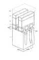
図1は、第1実施形態に係る不揮発性半導体記憶装置のメモリセルの概略構成を示す斜視図である。
図1において、半導体基板1には、ビット線方向DBにトレンチ2が形成され、半導体基板1に形成されるメモリセルのアクティブエリアが分離されている。なお、メモリセルにおけるアクティブエリアは、メモリセルに設けられたメモリトランジスタのチャネル領域および直列に接続されたメモリセル間の領域(例えばソース/ドレイン領域)を言う。また、半導体基板1の材質としては、例えば、Si、Ge、SiGe、SiC、SiSn、PbS、GaAs、InP、GaP、GaN、GaInAsPまたはZnSeなどから選択することができる。(First embodiment)
FIG. 1 is a perspective view showing a schematic configuration of a memory cell of the nonvolatile semiconductor memory device according to the first embodiment.
In FIG. 1, a
そして、トレンチ2には、埋め込み絶縁膜3が埋め込まれている。なお、埋め込み絶縁膜3は、例えば、CVD酸化膜やALD酸化膜またはCVD酸化膜やSOG酸化膜などの有機溶剤に可溶な無機ポリマーを用いることができる。なお、トレンチ2に埋め込まれる埋め込み絶縁膜の構成は必ずしも1層構造でなくてもよく、2層以上であってもよい。 A buried
また、半導体基板1上のアクティブエリアには、トンネル絶縁膜5を介して浮遊ゲート電極6がメモリセルごとに形成されている。この浮遊ゲート電極6は電荷蓄積層として用いることができる。なお、トンネル絶縁膜5としては、例えば、熱酸化膜であってもよいし、熱酸窒化膜であってもよい。あるいは、CVD酸化膜であってもよいし、CVD酸窒化膜であってもよい。あるいは、Siを挟んだ絶縁膜であってもよいし、Siがドット状に埋め込まれた絶縁膜であってもよい。浮遊ゲート電極6は、N型不純物またはP型不純物がドーピングされた多結晶シリコンであってもよいし、Mo、Ti、W、AlまたはTaなどを用いたメタル膜あるいはポリメタル膜であってもよい。 In the active area on the
浮遊ゲート電極6上には、電極間絶縁膜7を介して制御ゲート電極8がワード線方向DWに形成されている。なお、制御ゲート電極8は、ワード線の一部を構成することができる。ここで、浮遊ゲート電極6と制御ゲート電極8との間のカップリング比を向上させるため、浮遊ゲート電極6の側壁に回り込むように制御ゲート電極8を形成することができる。 A
制御ゲート電極8上には、シリサイド層9が形成され、シリサイド層9上には、カバー絶縁膜10が形成されている。なお、電極間絶縁膜7としては、例えば、シリコン酸化膜またはシリコン窒化膜を用いることができる。あるいは、ONO膜などのシリコン酸化膜とシリコン窒化膜との積層構造であってもよい。あるいは、酸化アルミニウムまたは酸化ハフニウムなどの高誘電率膜であってもよいし、シリコン酸化膜またはシリコン窒化膜などの低誘電率膜と高誘電率膜との積層構造であってもよい。制御ゲート電極8は、N型不純物またはP型不純物がドーピングされた多結晶シリコンであってもよい。あるいは、制御ゲート電極8は、Mo、Ti、W、AlまたはTaなどを用いたメタル膜あるいはポリメタル膜であってもよい。制御ゲート電極8としてメタル膜あるいはポリメタル膜を用いる場合、シリサイド層9はなくてもよい。シリサイド層9としては、例えば、CoSi、NiSi、PtSi、WSiまたはMoSiなどを用いることができる。また、カバー絶縁膜10としては、例えば、シリコン酸化膜を用いることができる。 A
ここで、トレンチ2内に埋め込まれた埋め込み絶縁膜3の一部が除去されることで、ワード線方向DWに隣接する浮遊ゲート電極6間に空隙AG1が形成されている。空隙AG1は、トレンチ2に入り込むように形成されることで、浮遊ゲート電極6の下面よりも深い位置まで至るようにしてもよい。また、空隙AG1は、制御ゲート電極8下に潜るようにしてトレンチ2に沿って連続して形成することができる。 Here, a part of the buried
また、カバー絶縁膜10は、浮遊ゲート電極6間が完全に埋め込まれないようにして制御ゲート電極8間に掛け渡される。このことで、ビット線方向DBに隣接する浮遊ゲート電極6間に空隙AG2が形成されている。なお、空隙AG2は、上下が非対称になるように形成することができ、その上端は尖塔形状を持つことができる。 Further, the
ここで、浮遊ゲート電極6間に空隙AG1、AG2(例えば、空気の比誘電率は1)を設けることにより、浮遊ゲート電極6間に絶縁体(例えば、シリコン酸化膜の比誘電率は3.9)が埋め込まれた場合に比べて浮遊ゲート電極間の寄生容量を低減することができる。このため、浮遊ゲート電極間の寄生容量に起因した隣接セル間の電界の干渉を低減することができ、セルトランジスタのしきい値電圧の分布幅を小さくすることができる。 Here, by providing the gaps AG1 and AG2 (for example, the relative dielectric constant of air is 1) between the floating
また、空隙AG1は、制御ゲート電極8下に潜るようにしてトレンチ2に沿って連続して形成することにより、制御ゲート電極8と半導体基板1との間のフリンジ容量を低減することができる。このため、浮遊ゲート電極6と制御ゲート電極8とのカップリング比を向上させることができ、書き込み電圧を低下させることができる。 Further, the fringe capacitance between the
(第2実施形態)
図2は、第2実施形態に係る不揮発性半導体記憶装置のメモリセルアレイの概略構成を示す回路図である。
図2において、メモリセル部R1には、セルトランジスタMTがロウ方向およびカラム方向にマトリックス状に配置されている。そして、複数のセルトランジスタMTが直列に接続され、この直列回路の両端にセレクトトランジスタSTが接続されることでNANDストリングNSが構成されている。また、カラム方向にはビット線BLが配置され、ロウ方向にはワード線WLおよびセレクトゲート電極SGが配置されている。(Second Embodiment)
FIG. 2 is a circuit diagram showing a schematic configuration of a memory cell array of the nonvolatile semiconductor memory device according to the second embodiment.
In FIG. 2, in the memory cell portion R1, cell transistors MT are arranged in a matrix in the row direction and the column direction. A plurality of cell transistors MT are connected in series, and a select transistor ST is connected to both ends of the series circuit to form a NAND string NS. A bit line BL is arranged in the column direction, and a word line WL and a select gate electrode SG are arranged in the row direction.
そして、同一カラムのNANDストリングNSは、セレクトトランジスタSTを介して同一のビット線BLに接続されている。そして、同一ロウのセルトランジスタMTは、同一のワード線WLに接続され、同一ロウのセレクトトランジスタSTは、同一のセレクトゲート電極SGに接続されることで、NANDブロックNBが構成されている。 The NAND strings NS in the same column are connected to the same bit line BL via the select transistor ST. The cell transistors MT in the same row are connected to the same word line WL, and the select transistors ST in the same row are connected to the same select gate electrode SG, thereby forming a NAND block NB.
また、メモリセル部R1の横にはワード線引き出し部R2が設けられている。ワード線引き出し部R2には、メモリセル部R1から引き出されたワード線WLおよびセレクトゲート電極SGが配置されている。 A word line lead portion R2 is provided beside the memory cell portion R1. In the word line lead portion R2, a word line WL and a select gate electrode SG drawn from the memory cell portion R1 are arranged.
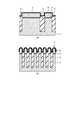
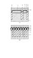
図3は、図2のRA部分の概略構成を示す平面図である。
図3において、ビット線方向DBにはトレンチTCが形成され、アクティブエリアAAはトレンチTCにて分離されている。また、ワード線方向DWには、ワード線WLおよびセレクトゲート電極SGが形成されている。そして、セレクトゲート電極SG間には、ビットコンタクト部R3が設けられ、ビットコンタクト部R3のアクティブエリアAA上には、ビットコンタクトBCが形成されている。また、ワード線引き出し部R2のアクティブエリアAA上には、メモリセル部R1から引き出されたワード線WLのコンタクトをとるワードコンタクトWCが設けられるとともに、メモリセル部R1から引き出されたセレクトゲート電極SGのコンタクトをとるセレクトゲートコンタクトSCが設けられている。FIG. 3 is a plan view showing a schematic configuration of the RA portion of FIG.
In FIG. 3, a trench TC is formed in the bit line direction DB, and the active area AA is separated by the trench TC. A word line WL and a select gate electrode SG are formed in the word line direction DW. A bit contact portion R3 is provided between the select gate electrodes SG, and a bit contact BC is formed on the active area AA of the bit contact portion R3. On the active area AA of the word line lead portion R2, a word contact WC that contacts the word line WL drawn from the memory cell portion R1 is provided, and a select gate electrode SG drawn from the memory cell portion R1. A select gate contact SC is provided to take this contact.
そして、メモリセル部R1のトレンチTC内では、図1の埋め込み絶縁膜3の一部が除去されることで、メモリセル部R1にはトレンチ2に沿って空隙AG1が形成されている。また、ワード線引き出し部R2のトレンチTC内では、図1の埋め込み絶縁膜3が除去されないようにすることで、ワード線引き出し部R2には空隙AG1が形成されないようにされている。ここで、空隙AG1は、制御ゲート電極8下に潜るようにして隣接するメモリセルに渡って連続して形成されるとともに、セレクトゲート電極SG下において分断されている。また、ビットコンタクト部R3のトレンチTCでは、埋め戻し絶縁膜RBが空隙AG1に埋め戻されることで、ビットコンタクト部R3では空隙AG1が除去されている。 Then, in the trench TC of the memory cell portion R1, a part of the buried insulating
ここで、ワード線引き出し部R2に空隙AG1が形成されないようにすることにより、ワード線引き出し部R2の広いトレンチTC上で細いワード線WLが空中に浮いたままになるのを防止することができる。このため、パターン飛びやパターン倒れなどを防止することができ、ワード線WL間でショート不良などが発生するのを抑制することができる。 Here, by preventing the gap AG1 from being formed in the word line lead portion R2, it is possible to prevent the thin word line WL from floating in the air on the wide trench TC of the word line lead portion R2. . For this reason, pattern skipping, pattern collapse, and the like can be prevented, and occurrence of a short circuit defect between the word lines WL can be suppressed.
また、ビットコンタクト部R3のトレンチTCでは、埋め戻し絶縁膜RBにて空隙AG1を埋め戻す。このことにより、ビットコンタクトBCの位置が左右いずれかのトレンチTC側にずれた場合においても、ビットコンタクトBCが空隙AG1を介して基板に突き抜けるのを防止することができる。 Further, in the trench TC of the bit contact portion R3, the gap AG1 is backfilled with the backfill insulating film RB. As a result, even when the position of the bit contact BC is shifted to the left or right trench TC, it is possible to prevent the bit contact BC from penetrating into the substrate via the gap AG1.
(第3実施形態)
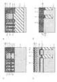
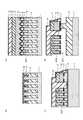
図4〜図26は、第3実施形態に係る不揮発性半導体記憶装置の製造方法を示す断面図である。なお、図4(b)〜図12(b)、図15(c)、図17(c)、図19(b)〜図26(b)は図3のA−A線で切断した断面図、図4(a)〜図12(a)、図16(c)、図18(c)は図3のA´−A´線で切断した断面図、図13(a)〜図15(a)、図17(a)、図19(c)〜図26(c)は図3のB−B線で切断した断面図、図13(b)、図16(a)、図18(a)は図3のB´−B´線で切断した断面図、図14(b)、図15(b)、図17(b)、図19(d)〜図26(d)は図3のC−C線で切断した断面図、図16(b)、図18(b)は図3のC´−C´線で切断した断面図、図15(d)、図17(d)、図19(a)〜図26(a)は図3のD−D線で切断した断面図、図16(d)、図18(d)は図3のD´−D´線で切断した断面図である。(Third embodiment)
4 to 26 are cross-sectional views illustrating the method for manufacturing the nonvolatile semiconductor memory device according to the third embodiment. 4 (b) to 12 (b), FIG. 15 (c), FIG. 17 (c), and FIG. 19 (b) to FIG. 26 (b) are cross-sectional views taken along line AA in FIG. 4 (a) to 12 (a), 16 (c), and 18 (c) are cross-sectional views taken along the line A'-A 'of FIG. 3, and FIGS. 13 (a) to 15 (a). ), FIG. 17 (a), FIG. 19 (c) to FIG. 26 (c) are cross-sectional views taken along line BB in FIG. 3, FIG. 13 (b), FIG. 16 (a), FIG. FIG. 14B, FIG. 15B, FIG. 17B, and FIGS. 19D to 26D are cross-sectional views taken along line B'-B 'of FIG. Cross-sectional views cut along line -C, FIGS. 16B and 18B are cross-sectional views cut along line C'-C 'in FIG. 3, FIGS. 15D, 17D, and 19 (A)-FIG. 26 (a) is sectional drawing cut | disconnected by the DD line | wire of FIG. 3, FIG.16 (d), FIG.18 (d) It is a cross-sectional view taken along a D'-D'line in FIG.
図4において、熱酸化などの方法を用いることにより、半導体基板1上にトンネル絶縁膜5を形成する。そして、CVDなどの方法を用いることにより、トンネル絶縁膜5上に浮遊ゲート電極材6´を成膜する。 In FIG. 4, a
次に、図5に示すように、CVDなどの方法を用いることにより、浮遊ゲート電極材6´上にハードマスクM1を形成する。なお、ハードマスクM1としては、例えば、シリコン酸化膜またはシリコン窒化膜を用いることができる。 Next, as shown in FIG. 5, a hard mask M1 is formed on the floating gate electrode material 6 'by using a method such as CVD. As the hard mask M1, for example, a silicon oxide film or a silicon nitride film can be used.
次に、図6に示すように、フォトリソグラフィ技術を用いることにより、開口部K1、K1´が設けられたレジストパターンR1をハードマスクM1上に形成する。 Next, as shown in FIG. 6, a resist pattern R1 having openings K1 and K1 ′ is formed on the hard mask M1 by using a photolithography technique.
次に、図7に示すように、レジストパターンR1をマスクとしてハードマスクM1をパターニングした後、そのハードマスクM1をマスクとして浮遊ゲート電極材6´、トンネル絶縁膜5および半導体基板1をエッチングすることにより、半導体基板1にトレンチ2、2´を形成する。 Next, as shown in FIG. 7, after patterning the hard mask M1 using the resist pattern R1 as a mask, the floating
次に、図8に示すように、CVDまたはSOG(塗布)などの方法を用いることにより、トレンチ2、2´全体が埋め込まれるようにして埋め込み絶縁膜3をハードマスクM1上に形成する。 Next, as shown in FIG. 8, by using a method such as CVD or SOG (coating), a buried insulating
次に、図9に示すように、CMPなどの方法を用いることにより、埋め込み絶縁膜3を薄膜化し、ハードマスクM1の表面を露出させる。 Next, as shown in FIG. 9, by using a method such as CMP, the buried insulating
次に、図10に示すように、ウェットエッチングなどの方法を用いることにより、ハードマスクM1を除去する。なお、ハードマスクM1がシリコン窒化膜の場合、ウェットエッチングの薬液はホット燐酸を用いることができる。そして、RIEなどの異方性エッチングを用いることにより、埋め込み絶縁膜3の一部を除去し、浮遊ゲート電極材6´の側壁の一部を露出させる。なお、浮遊ゲート電極材6´の側壁の一部を露出させる場合、埋め込み絶縁膜3は、トンネル絶縁膜5より上に残存させることが好ましい。また、埋め込み絶縁膜3がSOG酸化膜の場合、希フッ酸を用いたウェットエッチングにて埋め込み絶縁膜3の一部を除去するようにしてもよい。 Next, as shown in FIG. 10, the hard mask M1 is removed by using a method such as wet etching. In the case where the hard mask M1 is a silicon nitride film, hot phosphoric acid can be used as a chemical solution for wet etching. Then, by using anisotropic etching such as RIE, a part of the buried insulating
次に、図11に示すように、CVDなどの方法を用いることにより、浮遊ゲート電極材6´の側壁が覆われるようにして浮遊ゲート電極材6´上に電極間絶縁膜7を形成する。なお、電極間絶縁膜7は、例えば、ONO膜などの多層構造であってもよい。 Next, as shown in FIG. 11, by using a method such as CVD, an interelectrode
次に、図12に示すように、CVDなどの方法を用いることにより、制御ゲート電極材8´を電極間絶縁膜7上に成膜する。 Next, as shown in FIG. 12, a control
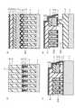
次に、図13に示すように、CVDなどの方法を用いることにより、キャップ絶縁膜11を制御ゲート電極材8´上に形成する。なお、キャップ絶縁膜11としては、例えば、シリコン酸化膜またはシリコン窒化膜を用いることができる。そして、スピンコートなどの方法を用いることにより、キャップ絶縁膜11上にレジスト膜R2を塗布する。 Next, as shown in FIG. 13, the
次に、図14に示すように、フォトリソグラフィ技術を用いることにより、レジスト膜R2に開口部K2を形成する。 Next, as shown in FIG. 14, an opening K2 is formed in the resist film R2 by using a photolithography technique.
次に、図15および図16に示すように、開口部K2が設けられたレジスト膜R2をマスクとしてキャップ絶縁膜11をパターニングした後、そのキャップ絶縁膜11をマスクとして制御ゲート電極材8´、電極間絶縁膜7および浮遊ゲート電極材6´をエッチングすることにより、メモリセルごとに分離された浮遊ゲート電極6を形成するとともに、電極間絶縁膜7を介して浮遊ゲート電極6上に配置された制御ゲート電極8およびセレクトゲート電極12をワード線方向に形成する。ここで、セレクトゲート電極12は、電極間絶縁膜7に設けられた開口部K2´を介してその下の浮遊ゲート電極6と接続される。 Next, as shown in FIGS. 15 and 16, after patterning the
ここで、例えば、埋め込み絶縁膜3および電極間絶縁膜7がシリコン酸化膜などの同様の材質の膜で構成されているものとすると、浮遊ゲート電極6の側壁の電極間絶縁膜7を縦方向にエッチングする分だけ埋め込み絶縁膜3がエッチングされる。このため、この時のトレンチ2、2´上の電極間絶縁膜7の下面から見た時の埋め込み絶縁膜3の落ち込み量Xは、トレンチ2、2´上の電極間絶縁膜7の下面から電荷蓄積層6上の電極間絶縁膜7の上面までの高さXとほぼ一致する。また、埋め込み絶縁膜3と浮遊ゲート電極材6´との選択比は100%でないので、浮遊ゲート電極材6´をエッチングする時にも埋め込み絶縁膜3がエッチングされ、埋め込み絶縁膜3はさらにα(α<X)分だけ落ち込む。 Here, for example, if the buried insulating
次に、図17および図18に示すように、フォトリソグラフィ技術を用いることにより、図3のワード線引き出し部R2が覆われるようにレジストパターンR3を埋め込み絶縁膜3およびキャップ絶縁膜11上に形成する。そして、ウェットエッチングなどの方法を用いることにより、図3のメモリセル部R1の埋め込み絶縁膜3の一部をトレンチ2に沿って除去し、ワード線方向DWに隣接する浮遊ゲート電極6間に空隙AG1を形成する。この時、空隙AG1は、制御ゲート電極8下に潜るようにしてトレンチ2に沿って連続して形成することができる。また、空隙AG1は、セレクトゲート電極12下で分断されるようにして、セレクトゲート電極12下の一部では埋め込み絶縁膜3が高さ方向に完全に残るようにすることができる。 Next, as shown in FIGS. 17 and 18, a resist pattern R3 is formed on the buried insulating
ここで、トレンチ2上では、制御ゲート電極8下が空隙AG1で繋がるようにするため、制御ゲート電極のゲート長L分だけ埋め込み絶縁膜3を横方向にエッチングする必要がある。この時、埋め込み絶縁膜3を横方向にエッチングする場合、埋め込み絶縁膜3は両側からエッチングされる。このため、埋め込み絶縁膜3は図15の状態からL/2だけさらに落ち込む。この時の埋め込み絶縁膜3のオーバーエッチング量をβ(β<L/2)とすると、トレンチ2上の電極間絶縁膜7の上面から見た時の空隙AG1の深さDは、X+α+L/2+βとなる。 Here, in order to connect the space below the
すなわち、α<Xかつβ<L/2という条件を考慮すると、トレンチ2上の電極間絶縁膜7の上面から見た時の空隙AG1の深さDは、X+L/2≦D<2X+Lという条件を満たす。 That is, considering the conditions of α <X and β <L / 2, the depth D of the air gap AG1 when viewed from the upper surface of the interelectrode
ここで、X+L/2≦D<2X+Lという条件を満たすように空隙AG1の深さDを設定することにより、埋め込み絶縁膜3のエッチング量を最小限に抑えつつ、制御ゲート電極8下が空隙AG1で繋がるように空隙AG1を形成することができる。このため、埋め込み絶縁膜3をエッチングする際にトンネル絶縁膜5および電極間絶縁膜7がエッチングされるのを抑制しつつ、浮遊ゲート電極6間の寄生容量に起因した隣接セル間の電界の干渉を低減することができる。 Here, by setting the depth D of the gap AG1 so as to satisfy the condition of X + L / 2 ≦ D <2X + L, the etching amount of the buried insulating
また、埋め込み絶縁膜3のウェットエッチングを行う際に、ワード線引き出し部R2をレジストパターンR3にて覆うことにより、ワード線引き出し部R2に空隙AG1が形成されないようにすることができる。このため、ワード線引き出し部R2の広いトレンチTC上で細いワード線WLが空中に浮いたままになるのを防止することができ、パターン飛びやパターン倒れなどを防止することができる。 Further, when the buried insulating
次に、図19に示すように、CVDなどの方法を用いることにより、露出面全体が覆われるようにスペーサ絶縁膜13を形成する。なお、スペーサ絶縁膜13としては、例えば、シリコン酸化膜を用いることができる。 Next, as shown in FIG. 19, by using a method such as CVD, a
次に、図20に示すように、プラズマCVDなどの方法を用いることにより、制御ゲート電極8間に架け渡されるようにカバー絶縁膜10を形成し、ビット線方向DBに隣接する浮遊ゲート電極6間に空隙AG2を形成する。なお、カバー絶縁膜10としては、例えば、シリコン酸化膜を用いることができる。また、制御ゲート電極8上にカバー絶縁膜10を形成する場合、空隙AG1、AG2がカバー絶縁膜10にて埋め込まれないようにするために、カバレッジの悪い条件に設定することができる。 Next, as shown in FIG. 20, by using a method such as plasma CVD, a
次に、図21に示すように、フォトリソグラフィ技術およびドライエッチング技術を用いることにより、図3のビットコンタクト部R3のカバー絶縁膜10を除去する。 Next, as shown in FIG. 21, the
次に、図22に示すように、CVDなどの方法を用いることにより、ビットコンタクト部R3のトレンチ2内が埋め戻されるように埋め戻し絶縁膜14をカバー絶縁膜10上に形成する。なお、埋め戻し絶縁膜14としては、例えば、シリコン酸化膜を用いることができる。 Next, as shown in FIG. 22, by using a method such as CVD, a
次に、図23に示すように、CVDなどの方法を用いることにより、埋め戻し絶縁膜14上にストッパ膜15を形成する。なお、ストッパ膜15としては、例えば、シリコン窒化膜を用いることができる。 Next, as shown in FIG. 23, a
次に、図24に示すように、CVDなどの方法を用いることにより、ストッパ膜15上に層間絶縁膜16を形成する。なお、層間絶縁膜16としては、例えば、NSG膜、PSG膜、BSG膜、BPSG膜またはHDP膜を用いることができる。そして、ストッパ膜15をストッパとしてCMPを行うことにより、層間絶縁膜16を平坦化する。 Next, as shown in FIG. 24, an
次に、図25に示すように、フォトリソグラフィ技術およびドライエッチング技術を用いることにより、図3のビットコンタクトBCに対応した開口部17を層間絶縁膜16に形成する。 Next, as shown in FIG. 25, an
次に、図26に示すように、コンタクト電極18を開口部17に埋め込むことにより、図3のビットコンタクト部R3にビットコンタクトBCを形成する。なお、コンタクト電極18は、例えば、n+多結晶シリコンまたはWなどの金属を用いることができる。Next, as shown in FIG. 26, the
ここで、ビットコンタクト部R3のトレンチ2内を埋め戻し絶縁膜14にて埋め戻すことにより、開口部17の位置がトレンチ2側にずれた場合においても、開口部17が半導体基板1に突き抜けるのを防止することができる。 Here, by filling the
(第4実施形態)
図27は、第4実施形態に係る不揮発性半導体記憶装置の製造方法を示す断面図である。なお、図27(a)は図3のD−D線で切断した断面図、図27(b)は図3のA−A線で切断した断面図、図27(c)は図3のB−B線で切断した断面図、図27(d)は図3のC−C線で切断した断面図である。(Fourth embodiment)
FIG. 27 is a cross-sectional view showing the method of manufacturing the nonvolatile semiconductor memory device according to the fourth embodiment. 27A is a cross-sectional view taken along the line D-D in FIG. 3, FIG. 27B is a cross-sectional view taken along the line A-A in FIG. 3, and FIG. FIG. 27D is a cross-sectional view taken along the line C-C in FIG. 3.
図27において、上述して第3実施形態では、図19の工程でスペーサ絶縁膜13を形成してから図20の工程でカバー絶縁膜10を形成する方法について説明したが、図19の工程でスペーサ絶縁膜13を形成することなく図20の工程でカバー絶縁膜10を形成するようにしてもよい。 27, in the third embodiment described above, the method of forming the
ここで、スペーサ絶縁膜13を省略することにより、スペーサ絶縁膜13の膜厚分だけ空隙AG1、AG2を拡大することができ、浮遊ゲート電極6間の寄生容量をより一層低減することができる。 Here, by omitting the
なお、スペーサ絶縁膜13を省略した場合、埋め戻し絶縁膜14またはストッパ膜15の膜厚を調整することにより、ビットコンタクト部R3のトレンチ2内を埋め戻すことができる。 If the
本発明のいくつかの実施形態を説明したが、これらの実施形態は、例として提示したものであり、発明の範囲を限定することは意図していない。これら新規な実施形態は、その他の様々な形態で実施されることが可能であり、発明の要旨を逸脱しない範囲で、種々の省略、置き換え、変更を行うことができる。これら実施形態やその変形は、発明の範囲や要旨に含まれるとともに、特許請求の範囲に記載された発明とその均等の範囲に含まれる。 Although several embodiments of the present invention have been described, these embodiments are presented by way of example and are not intended to limit the scope of the invention. These novel embodiments can be implemented in various other forms, and various omissions, replacements, and changes can be made without departing from the scope of the invention. These embodiments and modifications thereof are included in the scope and gist of the invention, and are included in the invention described in the claims and the equivalents thereof.
1 半導体基板、2、2´ トレンチ、3 埋め込み絶縁膜、5 トンネル絶縁膜、6 浮遊ゲート電極、7 電極間絶縁膜、8 制御ゲート電極、9 シリサイド層、10 カバー絶縁膜、AG1、AG2 空隙、R1 メモリセル部、R2 ワード線引き出し部、R3 ビットコンタクト部、NB NANDブロック、NS NANDストリング、BL ビット線、MT セルトランジスタ、ST セレクトトランジスタ、AA アクティブエリア、BC ビットコンタクト、WC ワードコンタクト、SC セレクトゲートコンタクト、WL ワード線、SG、12 セレクトゲート電極、RB 埋め戻し絶縁膜、6´ 浮遊ゲート電極材、8´ 制御ゲート電極材、M1 ハードマスク、R1〜R3 レジストパターン、K1、K2、K1´、K2´ 開口部、11 キャップ絶縁膜、13 スペーサ絶縁膜、14 埋め戻し絶縁膜、15 ストッパ膜、16 層間絶縁膜、17 開口部、18 コンタクト電極 DESCRIPTION OF
Claims (7)
Translated fromJapanese第1方向に延び、前記第1方向と交差する第2方向に互いに隣接するアクティブエリアに前記半導体基板を分割するトレンチと、
前記第2方向に延びる制御ゲート電極と、
前記第2方向に延び、前記制御ゲート電極のひとつに隣接するセレクトゲート電極と、
前記制御ゲート電極と前記半導体基板との間に配置された電荷蓄積層と、
前記セレクトゲート電極を含み、メモリセルのひとつとビット線との間に接続されたセレクトトランジスタと、
前記第1方向に延びるようにして前記トレンチ内に形成され、前記第2方向に隣接する電荷蓄積層間に配置されるとともに、前記セレクトゲート電極下に延びる空隙と、
前記セレクトゲート電極下に延びる空隙に隣接するようにして前記セレクトゲート電極下の前記トレンチ内に設けられた埋め込み絶縁膜とを備えることを特徴とする不揮発性半導体記憶装置。A semiconductor substrate;
A trench extending in a first direction and dividing the semiconductor substrate into active areas adjacent to each other in a second direction intersecting the first direction;
A control gate electrode extending in the second direction;
A select gate electrode extending in the second direction and adjacent to one of the control gate electrodes;
A charge storage layer disposed between the control gate electrode and the semiconductor substrate;
A select transistor including the select gate electrode and connected between one of the memory cells and the bit line;
A gap formed in the trench so as to extend in the first direction, disposed between the charge storage layers adjacent in the second direction, and extending under the select gate electrode;
A non-volatile semiconductor memory devicecomprising: a buried insulating film provided in the trench under the select gate electrode so as to be adjacent to a gap extending under the select gate electrode .
前記ワード線引き出し部のアクティブエリアを分離するトレンチ上では前記埋め込み絶縁膜と前記電極間絶縁膜が接していることを特徴とする請求項1から3のいずれか1項に記載の不揮発性半導体記憶装置。A word line lead portion in which a word line drawn from the memory cell is arranged;
The nonvolatile semiconductor memory according to any one of claims 1 to3 on the trench to isolate the active area of the word line lead portions, wherein the buried insulating film and the insulating film is in contact apparatus.
前記ビットコンタクト部のアクティブエリアを分離するトレンチ内に形成された空隙を埋め戻す埋め戻し絶縁膜をさらに備えることを特徴とする請求項1から4のいずれか1項に記載の不揮発性半導体記憶装置。A bit contact portion in which a bit contact is formed;
The nonvolatile semiconductor memory device according to any one of4 from claim 1, further comprising the bit contact part insulating film burying backfill voids formed in the trench to isolate the active area of the .
前記浮遊ゲート電極材および前記トンネル絶縁膜を介して前記半導体基板にトレンチをビット線方向に形成する工程と、
前記トレンチ内に埋め込み絶縁膜を形成する工程と、
前記埋め込み絶縁膜および前記浮遊ゲート電極材上に電極間絶縁膜を形成する工程と、
前記電極間絶縁膜上に制御ゲート電極材を成膜する工程と、
前記制御ゲート電極材、前記電極間絶縁膜および前記浮遊ゲート電極材をパターニングすることにより、メモリセルごとに分離された浮遊ゲート電極を形成するとともに、前記浮遊ゲート電極上に配置された制御ゲート電極をワード線方向に形成する工程と、
前記トレンチ内に埋め込まれた埋め込み絶縁膜の少なくとも一部を除去することで、前記ワード線下に潜るようにして前記トレンチに沿って配置された空隙を、前記ワード線方向に隣接する前記電荷蓄積層間に形成する工程とを備え、
前記トレンチ内に埋め込まれた埋め込み絶縁膜の少なくとも一部を除去する時に、前記メモリセルから引き出されたワード線が配置されるワード線引き出し部をレジストで覆うことを特徴とする不揮発性半導体記憶装置の製造方法。Forming a floating gate electrode material on a semiconductor substrate via a tunnel insulating film;
Forming a trench in the bit line direction in the semiconductor substrate via the floating gate electrode material and the tunnel insulating film;
Forming a buried insulating film in the trench;
Forming an interelectrode insulating film on the buried insulating film and the floating gate electrode material;
Forming a control gate electrode material on the interelectrode insulating film;
By patterning the control gate electrode material, the interelectrode insulating film, and the floating gate electrode material, a floating gate electrode separated for each memory cell is formed, and the control gate electrode disposed on the floating gate electrode Forming in the word line direction;
By removing at least a part of the buried insulating film buried in the trench, the charge accumulation adjacent to the word line in the gap arranged along the trench so as to be buried under the word line is performed. A step of forming between layers,
When removing at least a portion of the buried insulating film embedded in the trench, wherein the non-volatile semiconductor memoryyou characterized by covering the word line lead portions led out from the memory cell word lines are arranged in the resist Device manufacturing method.
前記浮遊ゲート電極材および前記トンネル絶縁膜を介して前記半導体基板にトレンチをビット線方向に形成する工程と、
前記トレンチ内に埋め込み絶縁膜を形成する工程と、
前記埋め込み絶縁膜および前記浮遊ゲート電極材上に電極間絶縁膜を形成する工程と、
前記電極間絶縁膜上に制御ゲート電極材を成膜する工程と、
前記制御ゲート電極材、前記電極間絶縁膜および前記浮遊ゲート電極材をパターニングすることにより、メモリセルごとに分離された浮遊ゲート電極を形成するとともに、前記浮遊ゲート電極上に配置された制御ゲート電極をワード線方向に形成する工程と、
前記トレンチ内に埋め込まれた埋め込み絶縁膜の少なくとも一部を除去することで、前記ワード線下に潜るようにして前記トレンチに沿って配置された空隙を、前記ワード線方向に隣接する前記電荷蓄積層間に形成する工程と、
前記トレンチ内に埋め込まれた埋め込み絶縁膜の少なくとも一部を除去した後、ビットコンタクトが形成されるビットコンタクト部のアクティブエリアを分離するトレンチ内に形成された空隙を埋め戻し絶縁膜にて埋め戻す工程とを備えることを特徴とする不揮発性半導体記憶装置の製造方法。Forming a floating gate electrode material on a semiconductor substrate via a tunnel insulating film;
Forming a trench in the bit line direction in the semiconductor substrate via the floating gate electrode material and the tunnel insulating film;
Forming a buried insulating film in the trench;
Forming an interelectrode insulating film on the buried insulating film and the floating gate electrode material;
Forming a control gate electrode material on the interelectrode insulating film;
By patterning the control gate electrode material, the interelectrode insulating film, and the floating gate electrode material, a floating gate electrode separated for each memory cell is formed, and the control gate electrode disposed on the floating gate electrode Forming in the word line direction;
By removing at least a part of the buried insulating film buried in the trench, the charge accumulation adjacent to the word line in the gap arranged along the trench so as to be buried under the word line is performed. Forming between the layers;
After removing at least a part of the buried insulating film buried in the trench, the void formed in the trench separating the active area of the bit contact portion where the bit contact is formed is filled back with the insulating film. A process for manufacturing a nonvolatile semiconductor memory device.
Priority Applications (4)
| Application Number | Priority Date | Filing Date | Title |
|---|---|---|---|
| JP2010258309AJP5570953B2 (en) | 2010-11-18 | 2010-11-18 | Nonvolatile semiconductor memory device and method of manufacturing nonvolatile semiconductor memory device |
| US13/237,425US9293547B2 (en) | 2010-11-18 | 2011-09-20 | NAND EEPROM with perpendicular sets of air gaps and method for manufacturing NAND EEPROM with perpendicular sets of air gaps |
| SG2011069010ASG181213A1 (en) | 2010-11-18 | 2011-09-21 | Nonvolatile semiconductor memory device and method for manufacturing nonvolatile semiconductor memory device |
| SG2014009864ASG2014009864A (en) | 2010-11-18 | 2011-09-21 | Nonvolatile semiconductor memory device and method for manufacturing nonvolatile semiconductor memory device |
Applications Claiming Priority (1)
| Application Number | Priority Date | Filing Date | Title |
|---|---|---|---|
| JP2010258309AJP5570953B2 (en) | 2010-11-18 | 2010-11-18 | Nonvolatile semiconductor memory device and method of manufacturing nonvolatile semiconductor memory device |
Publications (2)
| Publication Number | Publication Date |
|---|---|
| JP2012109466A JP2012109466A (en) | 2012-06-07 |
| JP5570953B2true JP5570953B2 (en) | 2014-08-13 |
Family
ID=46063531
Family Applications (1)
| Application Number | Title | Priority Date | Filing Date |
|---|---|---|---|
| JP2010258309AActiveJP5570953B2 (en) | 2010-11-18 | 2010-11-18 | Nonvolatile semiconductor memory device and method of manufacturing nonvolatile semiconductor memory device |
Country Status (3)
| Country | Link |
|---|---|
| US (1) | US9293547B2 (en) |
| JP (1) | JP5570953B2 (en) |
| SG (2) | SG181213A1 (en) |
Families Citing this family (29)
| Publication number | Priority date | Publication date | Assignee | Title |
|---|---|---|---|---|
| US8946048B2 (en) | 2010-06-19 | 2015-02-03 | Sandisk Technologies Inc. | Method of fabricating non-volatile memory with flat cell structures and air gap isolation |
| US8603890B2 (en) | 2010-06-19 | 2013-12-10 | Sandisk Technologies Inc. | Air gap isolation in non-volatile memory |
| US8492224B2 (en) | 2010-06-20 | 2013-07-23 | Sandisk Technologies Inc. | Metal control gate structures and air gap isolation in non-volatile memory |
| JP5591668B2 (en)* | 2010-11-30 | 2014-09-17 | 株式会社東芝 | Nonvolatile semiconductor memory device and method of manufacturing nonvolatile semiconductor memory device |
| US8778749B2 (en) | 2011-01-12 | 2014-07-15 | Sandisk Technologies Inc. | Air isolation in high density non-volatile memory |
| US9136128B2 (en) | 2011-08-31 | 2015-09-15 | Micron Technology, Inc. | Methods and apparatuses including memory cells with air gaps and other low dielectric constant materials |
| KR101556867B1 (en)* | 2011-09-22 | 2015-10-01 | 인텔 코포레이션 | Use of etch process post wordline definition to improve data retention in a flash memory device |
| US9123714B2 (en) | 2012-02-16 | 2015-09-01 | Sandisk Technologies Inc. | Metal layer air gap formation |
| JP2013197482A (en)* | 2012-03-22 | 2013-09-30 | Toshiba Corp | Nonvolatile semiconductor storage device manufacturing method and nonvolatile semiconductor storage device |
| KR101926359B1 (en)* | 2012-04-06 | 2018-12-07 | 삼성전자주식회사 | Semiconductor device and method for fabricating the same |
| US20130307044A1 (en)* | 2012-05-15 | 2013-11-21 | Hiroyuki Kinoshita | Selective Air Gap Isolation In Non-Volatile Memory |
| KR101986126B1 (en)* | 2012-07-18 | 2019-06-05 | 삼성전자주식회사 | Non volatile memory devices and methods of manufacturing the same |
| KR20140020476A (en)* | 2012-08-08 | 2014-02-19 | 에스케이하이닉스 주식회사 | Semiconductor memory device and manufacturing method thereof |
| US20140138761A1 (en)* | 2012-11-16 | 2014-05-22 | Kabushiki Kaisha Toshiba | Semiconductor device and manufacturing method of semiconductor device |
| US9123577B2 (en) | 2012-12-12 | 2015-09-01 | Sandisk Technologies Inc. | Air gap isolation in non-volatile memory using sacrificial films |
| JP2014138101A (en)* | 2013-01-17 | 2014-07-28 | Toshiba Corp | Nonvolatile semiconductor storage device and manufacturing method of the same |
| JP2014157123A (en) | 2013-02-18 | 2014-08-28 | Toshiba Corp | Sample, sample preparation device and sample observation method |
| KR20140109105A (en) | 2013-03-05 | 2014-09-15 | 에스케이하이닉스 주식회사 | Semiconductor device and method of manufacturing the same |
| JP6176844B2 (en) | 2013-08-06 | 2017-08-09 | 東芝メモリ株式会社 | Nonvolatile semiconductor memory device |
| US9257570B2 (en) | 2013-09-12 | 2016-02-09 | Kabushiki Kaisha Toshiba | Semiconductor memory device and method for manufacturing the same |
| US9349740B2 (en) | 2014-01-24 | 2016-05-24 | Sandisk Technologies Inc. | Non-volatile storage element with suspended charge storage region |
| CN104835773B (en)* | 2014-02-08 | 2018-12-21 | 中芯国际集成电路制造(上海)有限公司 | A method of making semiconductor devices |
| US10446572B2 (en) | 2017-08-11 | 2019-10-15 | Micron Technology, Inc. | Void formation for charge trap structures |
| US10453855B2 (en) | 2017-08-11 | 2019-10-22 | Micron Technology, Inc. | Void formation in charge trap structures |
| US10680006B2 (en) | 2017-08-11 | 2020-06-09 | Micron Technology, Inc. | Charge trap structure with barrier to blocking region |
| US10164009B1 (en) | 2017-08-11 | 2018-12-25 | Micron Technology, Inc. | Memory device including voids between control gates |
| US11309433B2 (en)* | 2020-03-18 | 2022-04-19 | Winbond Electronics Corp. | Non-volatile memory structure and manufacturing method thereof |
| CN113540105B (en)* | 2020-04-14 | 2023-11-03 | 中芯国际集成电路制造(上海)有限公司 | Semiconductor device and forming method |
| US12176440B2 (en)* | 2021-11-03 | 2024-12-24 | Winbond Electronics Corp. | Semiconductor structure with an air gap and method of forming the same |
Family Cites Families (66)
| Publication number | Priority date | Publication date | Assignee | Title |
|---|---|---|---|---|
| US4979004A (en) | 1988-01-29 | 1990-12-18 | Texas Instruments Incorporated | Floating gate memory cell and device |
| US5792706A (en) | 1996-06-05 | 1998-08-11 | Advanced Micro Devices, Inc. | Interlevel dielectric with air gaps to reduce permitivity |
| US5783481A (en) | 1996-06-05 | 1998-07-21 | Advanced Micro Devices, Inc. | Semiconductor interlevel dielectric having a polymide for producing air gaps |
| US5880026A (en) | 1996-12-23 | 1999-03-09 | Texas Instruments Incorporated | Method for air gap formation by plasma treatment of aluminum interconnects |
| JPH11126819A (en) | 1997-06-20 | 1999-05-11 | Nippon Steel Corp | Semiconductor device and manufacturing method thereof |
| US6211561B1 (en) | 1998-11-16 | 2001-04-03 | Conexant Systems, Inc. | Interconnect structure and method employing air gaps between metal lines and between metal layers |
| US6071805A (en) | 1999-01-25 | 2000-06-06 | Chartered Semiconductor Manufacturing, Ltd. | Air gap formation for high speed IC processing |
| US6022802A (en) | 1999-03-18 | 2000-02-08 | Taiwan Semiconductor Manufacturing Company | Low dielectric constant intermetal dielectric (IMD) by formation of air gap between metal lines |
| US6815329B2 (en) | 2000-02-08 | 2004-11-09 | International Business Machines Corporation | Multilayer interconnect structure containing air gaps and method for making |
| JP4493182B2 (en) | 2000-08-23 | 2010-06-30 | 株式会社ルネサステクノロジ | Semiconductor device |
| MY128644A (en) | 2000-08-31 | 2007-02-28 | Georgia Tech Res Inst | Fabrication of semiconductor devices with air gaps for ultra low capacitance interconnections and methods of making same |
| TWI227043B (en) | 2000-09-01 | 2005-01-21 | Koninkl Philips Electronics Nv | Method of manufacturing a semiconductor device |
| KR100396470B1 (en)* | 2001-02-19 | 2003-09-03 | 삼성전자주식회사 | Non-volatile memory device having bitline contact pad and Method of manufacturing the same |
| KR100436673B1 (en)* | 2001-05-28 | 2004-07-02 | 가부시끼가이샤 도시바 | Semiconductor device and manufacturing method thereof |
| JP4439142B2 (en) | 2001-06-26 | 2010-03-24 | 株式会社東芝 | Method for manufacturing nonvolatile semiconductor memory |
| US6825058B2 (en)* | 2001-06-28 | 2004-11-30 | Sharp Laboratories Of America, Inc. | Methods of fabricating trench isolated cross-point memory array |
| US6627529B2 (en) | 2002-02-07 | 2003-09-30 | Micron Technology, Inc. | Capacitance reduction by tunnel formation for use with semiconductor device |
| DE10255117A1 (en) | 2002-11-26 | 2004-06-17 | Infineon Technologies Ag | Semiconductor memory device and method for its production |
| US7045849B2 (en) | 2003-05-21 | 2006-05-16 | Sandisk Corporation | Use of voids between elements in semiconductor structures for isolation |
| JP2005039216A (en) | 2003-06-23 | 2005-02-10 | Toshiba Corp | Nonvolatile semiconductor memory device |
| JP2005026589A (en)* | 2003-07-04 | 2005-01-27 | Toshiba Corp | Semiconductor memory device and manufacturing method thereof |
| US7169667B2 (en) | 2003-07-30 | 2007-01-30 | Promos Technologies Inc. | Nonvolatile memory cell with multiple floating gates formed after the select gate |
| JP2005116970A (en) | 2003-10-10 | 2005-04-28 | Toshiba Corp | Nonvolatile semiconductor memory device |
| US7238575B2 (en) | 2004-03-10 | 2007-07-03 | Promos Technologies, Inc. | Fabrication of conductive lines interconnecting conductive gates in nonvolatile memories, and non-volatile memory structures |
| JP4331070B2 (en) | 2004-08-06 | 2009-09-16 | 株式会社東芝 | Semiconductor memory device |
| JP2006196843A (en)* | 2005-01-17 | 2006-07-27 | Toshiba Corp | Semiconductor device and manufacturing method thereof |
| US7259038B2 (en) | 2005-01-19 | 2007-08-21 | Sandisk Corporation | Forming nonvolatile phase change memory cell having a reduced thermal contact area |
| JP2006228893A (en) | 2005-02-16 | 2006-08-31 | Renesas Technology Corp | Semiconductor device and its manufacturing method |
| US7348618B2 (en) | 2005-03-30 | 2008-03-25 | Intel Corporation | Flash memory cell having reduced floating gate to floating gate coupling |
| JP2006302950A (en) | 2005-04-15 | 2006-11-02 | Renesas Technology Corp | Nonvolatile semiconductor device and method of manufacturing nonvolatile semiconductor device |
| JP4316540B2 (en) | 2005-06-24 | 2009-08-19 | 株式会社東芝 | Nonvolatile semiconductor memory device and method for manufacturing nonvolatile semiconductor memory device |
| JP4731262B2 (en) | 2005-09-22 | 2011-07-20 | ルネサスエレクトロニクス株式会社 | Nonvolatile semiconductor memory device and method of manufacturing nonvolatile semiconductor memory device |
| KR100784860B1 (en) | 2005-10-31 | 2007-12-14 | 삼성전자주식회사 | Nonvolatile Memory Device and Manufacturing Method Thereof |
| EP1804293A1 (en) | 2005-12-30 | 2007-07-04 | STMicroelectronics S.r.l. | Process for manufacturing a non volatile memory electronic device |
| JP2007250656A (en)* | 2006-03-14 | 2007-09-27 | Toshiba Corp | Semiconductor device and manufacturing method thereof |
| EP1835530A3 (en)* | 2006-03-17 | 2009-01-28 | Samsung Electronics Co., Ltd. | Non-volatile memory device and method of manufacturing the same |
| JP4762041B2 (en)* | 2006-04-24 | 2011-08-31 | 株式会社東芝 | Nonvolatile semiconductor memory |
| JP2007299975A (en) | 2006-05-01 | 2007-11-15 | Renesas Technology Corp | Semiconductor device, and its manufacturing method |
| EP1881527A1 (en)* | 2006-07-17 | 2008-01-23 | STMicroelectronics S.r.l. | Process for manufacturing a semiconductor wafer having SOI-insulated wells and semiconductor wafer thereby manufactured |
| US7881113B2 (en) | 2007-02-07 | 2011-02-01 | Micron Technology, Inc. | Relaxed metal pitch memory architectures |
| JP2008283095A (en)* | 2007-05-14 | 2008-11-20 | Toshiba Corp | Nonvolatile semiconductor memory device and manufacturing method thereof |
| JP2009010088A (en)* | 2007-06-27 | 2009-01-15 | Toshiba Corp | Semiconductor device and manufacturing method thereof |
| JP2009059931A (en) | 2007-08-31 | 2009-03-19 | Toshiba Corp | Nonvolatile semiconductor memory device |
| US20090087562A1 (en) | 2007-09-27 | 2009-04-02 | Long Hua Lee | Method of preparing cross-linked organic glasses for air-gap sacrificial layers |
| US7829268B2 (en) | 2007-10-17 | 2010-11-09 | Tokyo Electron Limited | Method for air gap formation using UV-decomposable materials |
| JP2009194244A (en)* | 2008-02-15 | 2009-08-27 | Toshiba Corp | Semiconductor memory device and manufacturing method thereof |
| JP4703669B2 (en)* | 2008-02-18 | 2011-06-15 | 株式会社東芝 | Semiconductor memory device and manufacturing method thereof |
| JP4729060B2 (en) | 2008-02-26 | 2011-07-20 | 株式会社東芝 | Manufacturing method of semiconductor memory device |
| JP2009212218A (en) | 2008-03-03 | 2009-09-17 | Toshiba Corp | Semiconductor storage device and method for manufacturing the same |
| JP4956500B2 (en)* | 2008-07-22 | 2012-06-20 | 株式会社東芝 | Semiconductor memory device and manufacturing method thereof |
| JP2010080853A (en)* | 2008-09-29 | 2010-04-08 | Toshiba Corp | Nonvolatile semiconductor storage device, and method for manufacturing the same |
| JP2010087159A (en) | 2008-09-30 | 2010-04-15 | Toshiba Corp | Nonvolatile semiconductor storage and method of manufacturing the same |
| US8105867B2 (en) | 2008-11-18 | 2012-01-31 | Sandisk 3D Llc | Self-aligned three-dimensional non-volatile memory fabrication |
| JP2010153458A (en) | 2008-12-24 | 2010-07-08 | Toshiba Corp | Method of manufacturing semiconductor device, and semiconductor device |
| JP2010153623A (en)* | 2008-12-25 | 2010-07-08 | Toshiba Corp | Method of manufacturing semiconductor device |
| JP2010161301A (en)* | 2009-01-09 | 2010-07-22 | Toshiba Corp | Semiconductor memory device and method of manufacturing the same |
| KR20100102982A (en)* | 2009-03-12 | 2010-09-27 | 삼성전자주식회사 | Semiconductor device |
| JP4923078B2 (en) | 2009-03-23 | 2012-04-25 | 株式会社東芝 | Semiconductor memory device and method of manufacturing the semiconductor memory device |
| JP2010272638A (en) | 2009-05-20 | 2010-12-02 | Toshiba Corp | Semiconductor memory device and manufacturing method thereof |
| US8546239B2 (en) | 2010-06-11 | 2013-10-01 | Sandisk Technologies Inc. | Methods of fabricating non-volatile memory with air gaps |
| US8603890B2 (en)* | 2010-06-19 | 2013-12-10 | Sandisk Technologies Inc. | Air gap isolation in non-volatile memory |
| US8946048B2 (en)* | 2010-06-19 | 2015-02-03 | Sandisk Technologies Inc. | Method of fabricating non-volatile memory with flat cell structures and air gap isolation |
| US8492224B2 (en)* | 2010-06-20 | 2013-07-23 | Sandisk Technologies Inc. | Metal control gate structures and air gap isolation in non-volatile memory |
| KR20120025315A (en) | 2010-09-07 | 2012-03-15 | 삼성전자주식회사 | Semiconductor deivces and methods of fabricating the same |
| SG181212A1 (en) | 2010-11-18 | 2012-06-28 | Toshiba Kk | Nonvolatile semiconductor memory and method of manufacturing with multiple air gaps |
| JP2013105990A (en) | 2011-11-16 | 2013-05-30 | Toshiba Corp | Nonvolatile semiconductor storage device |
- 2010
- 2010-11-18JPJP2010258309Apatent/JP5570953B2/enactiveActive
- 2011
- 2011-09-20USUS13/237,425patent/US9293547B2/enactiveActive
- 2011-09-21SGSG2011069010Apatent/SG181213A1/enunknown
- 2011-09-21SGSG2014009864Apatent/SG2014009864A/enunknown
Also Published As
| Publication number | Publication date |
|---|---|
| JP2012109466A (en) | 2012-06-07 |
| SG2014009864A (en) | 2014-05-29 |
| US9293547B2 (en) | 2016-03-22 |
| US20120126303A1 (en) | 2012-05-24 |
| SG181213A1 (en) | 2012-06-28 |
Similar Documents
| Publication | Publication Date | Title |
|---|---|---|
| JP5570953B2 (en) | Nonvolatile semiconductor memory device and method of manufacturing nonvolatile semiconductor memory device | |
| US10937797B2 (en) | Three-dimensional semiconductor memory devices | |
| US10546869B2 (en) | Semiconductor device | |
| CN107359165B (en) | vertical memory device | |
| KR102644525B1 (en) | A vertical semiconductor device | |
| KR102461150B1 (en) | Three dimensional semiconductor device | |
| KR102553126B1 (en) | Memory Device Having Channel Structure | |
| US8980712B2 (en) | 3D non-volatile memory device and method for fabricating the same | |
| CN102769018B (en) | Nonvolatile semiconductor memory member | |
| JP5591668B2 (en) | Nonvolatile semiconductor memory device and method of manufacturing nonvolatile semiconductor memory device | |
| US20170278936A1 (en) | Semiconductor devices and methods of manufacturing the same | |
| KR101747577B1 (en) | Local buried channel dielectric for vertical nand performance enhancement and vertical scaling | |
| US11778825B2 (en) | Method of fabricating a vertical semiconductor device | |
| US11456316B2 (en) | Semiconductor device having word line separation layer | |
| JP5796029B2 (en) | Semiconductor device and manufacturing method of semiconductor device | |
| US11728246B2 (en) | Semiconductor device having a stack including electrodes vertically stacked on a substrate and electronic system including the same | |
| JP2008244485A (en) | Nonvolatile memory device and manufacturing method thereof | |
| KR20150126524A (en) | Semiconductor Memory Device And Method of Fabricating The Same | |
| KR102728797B1 (en) | Semiconductor devices and operating method for the same | |
| KR20150116175A (en) | Non-volatile memory device for reducing resistance of source line | |
| JP5388993B2 (en) | Nonvolatile semiconductor memory device and method of manufacturing nonvolatile semiconductor memory device | |
| US20140042513A1 (en) | Non-volatile semiconductor storage device | |
| JP2012199313A (en) | Nonvolatile semiconductor memory device | |
| JP5591667B2 (en) | Nonvolatile semiconductor memory device and method of manufacturing nonvolatile semiconductor memory device | |
| US20130119450A1 (en) | Non-volatile semiconductor storage device |
Legal Events
| Date | Code | Title | Description |
|---|---|---|---|
| A621 | Written request for application examination | Free format text:JAPANESE INTERMEDIATE CODE: A621 Effective date:20130218 | |
| A131 | Notification of reasons for refusal | Free format text:JAPANESE INTERMEDIATE CODE: A131 Effective date:20140204 | |
| A521 | Request for written amendment filed | Free format text:JAPANESE INTERMEDIATE CODE: A523 Effective date:20140407 | |
| TRDD | Decision of grant or rejection written | ||
| A01 | Written decision to grant a patent or to grant a registration (utility model) | Free format text:JAPANESE INTERMEDIATE CODE: A01 Effective date:20140527 | |
| A61 | First payment of annual fees (during grant procedure) | Free format text:JAPANESE INTERMEDIATE CODE: A61 Effective date:20140625 | |
| R151 | Written notification of patent or utility model registration | Ref document number:5570953 Country of ref document:JP Free format text:JAPANESE INTERMEDIATE CODE: R151 | |
| S111 | Request for change of ownership or part of ownership | Free format text:JAPANESE INTERMEDIATE CODE: R313111 | |
| R350 | Written notification of registration of transfer | Free format text:JAPANESE INTERMEDIATE CODE: R350 | |
| S111 | Request for change of ownership or part of ownership | Free format text:JAPANESE INTERMEDIATE CODE: R313111 | |
| R350 | Written notification of registration of transfer | Free format text:JAPANESE INTERMEDIATE CODE: R350 |