JP5569173B2 - Semiconductor device manufacturing method and semiconductor device - Google Patents
Semiconductor device manufacturing method and semiconductor deviceDownload PDFInfo
- Publication number
- JP5569173B2 JP5569173B2JP2010139847AJP2010139847AJP5569173B2JP 5569173 B2JP5569173 B2JP 5569173B2JP 2010139847 AJP2010139847 AJP 2010139847AJP 2010139847 AJP2010139847 AJP 2010139847AJP 5569173 B2JP5569173 B2JP 5569173B2
- Authority
- JP
- Japan
- Prior art keywords
- region
- gate electrode
- film
- gate
- forming
- Prior art date
- Legal status (The legal status is an assumption and is not a legal conclusion. Google has not performed a legal analysis and makes no representation as to the accuracy of the status listed.)
- Expired - Fee Related
Links
Images


Classifications
- H—ELECTRICITY
- H01—ELECTRIC ELEMENTS
- H01L—SEMICONDUCTOR DEVICES NOT COVERED BY CLASS H10
- H01L21/00—Processes or apparatus adapted for the manufacture or treatment of semiconductor or solid state devices or of parts thereof
- H01L21/02—Manufacture or treatment of semiconductor devices or of parts thereof
- H01L21/04—Manufacture or treatment of semiconductor devices or of parts thereof the devices having potential barriers, e.g. a PN junction, depletion layer or carrier concentration layer
- H01L21/18—Manufacture or treatment of semiconductor devices or of parts thereof the devices having potential barriers, e.g. a PN junction, depletion layer or carrier concentration layer the devices having semiconductor bodies comprising elements of Group IV of the Periodic Table or AIIIBV compounds with or without impurities, e.g. doping materials
- H01L21/28—Manufacture of electrodes on semiconductor bodies using processes or apparatus not provided for in groups H01L21/20 - H01L21/268
- H01L21/28008—Making conductor-insulator-semiconductor electrodes
- H01L21/28017—Making conductor-insulator-semiconductor electrodes the insulator being formed after the semiconductor body, the semiconductor being silicon
- H01L21/28026—Making conductor-insulator-semiconductor electrodes the insulator being formed after the semiconductor body, the semiconductor being silicon characterised by the conductor
- H01L21/28114—Making conductor-insulator-semiconductor electrodes the insulator being formed after the semiconductor body, the semiconductor being silicon characterised by the conductor characterised by the sectional shape, e.g. T, inverted-T
- H—ELECTRICITY
- H10—SEMICONDUCTOR DEVICES; ELECTRIC SOLID-STATE DEVICES NOT OTHERWISE PROVIDED FOR
- H10D—INORGANIC ELECTRIC SEMICONDUCTOR DEVICES
- H10D30/00—Field-effect transistors [FET]
- H10D30/60—Insulated-gate field-effect transistors [IGFET]
- H10D30/791—Arrangements for exerting mechanical stress on the crystal lattice of the channel regions
- H10D30/792—Arrangements for exerting mechanical stress on the crystal lattice of the channel regions comprising applied insulating layers, e.g. stress liners
- H—ELECTRICITY
- H10—SEMICONDUCTOR DEVICES; ELECTRIC SOLID-STATE DEVICES NOT OTHERWISE PROVIDED FOR
- H10D—INORGANIC ELECTRIC SEMICONDUCTOR DEVICES
- H10D64/00—Electrodes of devices having potential barriers
- H10D64/01—Manufacture or treatment
- H10D64/017—Manufacture or treatment using dummy gates in processes wherein at least parts of the final gates are self-aligned to the dummy gates, i.e. replacement gate processes
- H—ELECTRICITY
- H10—SEMICONDUCTOR DEVICES; ELECTRIC SOLID-STATE DEVICES NOT OTHERWISE PROVIDED FOR
- H10D—INORGANIC ELECTRIC SEMICONDUCTOR DEVICES
- H10D64/00—Electrodes of devices having potential barriers
- H10D64/20—Electrodes characterised by their shapes, relative sizes or dispositions
- H10D64/27—Electrodes not carrying the current to be rectified, amplified, oscillated or switched, e.g. gates
- H10D64/311—Gate electrodes for field-effect devices
- H10D64/411—Gate electrodes for field-effect devices for FETs
- H10D64/511—Gate electrodes for field-effect devices for FETs for IGFETs
- H10D64/517—Gate electrodes for field-effect devices for FETs for IGFETs characterised by the conducting layers
- H10D64/518—Gate electrodes for field-effect devices for FETs for IGFETs characterised by the conducting layers characterised by their lengths or sectional shapes
- H—ELECTRICITY
- H10—SEMICONDUCTOR DEVICES; ELECTRIC SOLID-STATE DEVICES NOT OTHERWISE PROVIDED FOR
- H10D—INORGANIC ELECTRIC SEMICONDUCTOR DEVICES
- H10D84/00—Integrated devices formed in or on semiconductor substrates that comprise only semiconducting layers, e.g. on Si wafers or on GaAs-on-Si wafers
- H10D84/01—Manufacture or treatment
- H10D84/0123—Integrating together multiple components covered by H10D12/00 or H10D30/00, e.g. integrating multiple IGBTs
- H10D84/0126—Integrating together multiple components covered by H10D12/00 or H10D30/00, e.g. integrating multiple IGBTs the components including insulated gates, e.g. IGFETs
- H10D84/0165—Integrating together multiple components covered by H10D12/00 or H10D30/00, e.g. integrating multiple IGBTs the components including insulated gates, e.g. IGFETs the components including complementary IGFETs, e.g. CMOS devices
- H10D84/0167—Manufacturing their channels
- H—ELECTRICITY
- H10—SEMICONDUCTOR DEVICES; ELECTRIC SOLID-STATE DEVICES NOT OTHERWISE PROVIDED FOR
- H10D—INORGANIC ELECTRIC SEMICONDUCTOR DEVICES
- H10D84/00—Integrated devices formed in or on semiconductor substrates that comprise only semiconducting layers, e.g. on Si wafers or on GaAs-on-Si wafers
- H10D84/01—Manufacture or treatment
- H10D84/0123—Integrating together multiple components covered by H10D12/00 or H10D30/00, e.g. integrating multiple IGBTs
- H10D84/0126—Integrating together multiple components covered by H10D12/00 or H10D30/00, e.g. integrating multiple IGBTs the components including insulated gates, e.g. IGFETs
- H10D84/0165—Integrating together multiple components covered by H10D12/00 or H10D30/00, e.g. integrating multiple IGBTs the components including insulated gates, e.g. IGFETs the components including complementary IGFETs, e.g. CMOS devices
- H10D84/0172—Manufacturing their gate conductors
- H10D84/0177—Manufacturing their gate conductors the gate conductors having different materials or different implants
- H—ELECTRICITY
- H10—SEMICONDUCTOR DEVICES; ELECTRIC SOLID-STATE DEVICES NOT OTHERWISE PROVIDED FOR
- H10D—INORGANIC ELECTRIC SEMICONDUCTOR DEVICES
- H10D84/00—Integrated devices formed in or on semiconductor substrates that comprise only semiconducting layers, e.g. on Si wafers or on GaAs-on-Si wafers
- H10D84/01—Manufacture or treatment
- H10D84/0123—Integrating together multiple components covered by H10D12/00 or H10D30/00, e.g. integrating multiple IGBTs
- H10D84/0126—Integrating together multiple components covered by H10D12/00 or H10D30/00, e.g. integrating multiple IGBTs the components including insulated gates, e.g. IGFETs
- H10D84/0165—Integrating together multiple components covered by H10D12/00 or H10D30/00, e.g. integrating multiple IGBTs the components including insulated gates, e.g. IGFETs the components including complementary IGFETs, e.g. CMOS devices
- H10D84/0186—Manufacturing their interconnections or electrodes, e.g. source or drain electrodes
- H—ELECTRICITY
- H10—SEMICONDUCTOR DEVICES; ELECTRIC SOLID-STATE DEVICES NOT OTHERWISE PROVIDED FOR
- H10D—INORGANIC ELECTRIC SEMICONDUCTOR DEVICES
- H10D84/00—Integrated devices formed in or on semiconductor substrates that comprise only semiconducting layers, e.g. on Si wafers or on GaAs-on-Si wafers
- H10D84/01—Manufacture or treatment
- H10D84/02—Manufacture or treatment characterised by using material-based technologies
- H10D84/03—Manufacture or treatment characterised by using material-based technologies using Group IV technology, e.g. silicon technology or silicon-carbide [SiC] technology
- H10D84/038—Manufacture or treatment characterised by using material-based technologies using Group IV technology, e.g. silicon technology or silicon-carbide [SiC] technology using silicon technology, e.g. SiGe
- H—ELECTRICITY
- H01—ELECTRIC ELEMENTS
- H01L—SEMICONDUCTOR DEVICES NOT COVERED BY CLASS H10
- H01L2924/00—Indexing scheme for arrangements or methods for connecting or disconnecting semiconductor or solid-state bodies as covered by H01L24/00
- H01L2924/0001—Technical content checked by a classifier
- H01L2924/0002—Not covered by any one of groups H01L24/00, H01L24/00 and H01L2224/00
- H—ELECTRICITY
- H10—SEMICONDUCTOR DEVICES; ELECTRIC SOLID-STATE DEVICES NOT OTHERWISE PROVIDED FOR
- H10D—INORGANIC ELECTRIC SEMICONDUCTOR DEVICES
- H10D30/00—Field-effect transistors [FET]
- H10D30/60—Insulated-gate field-effect transistors [IGFET]
- H10D30/601—Insulated-gate field-effect transistors [IGFET] having lightly-doped drain or source extensions, e.g. LDD IGFETs or DDD IGFETs
Landscapes
- Engineering & Computer Science (AREA)
- Physics & Mathematics (AREA)
- Condensed Matter Physics & Semiconductors (AREA)
- General Physics & Mathematics (AREA)
- Manufacturing & Machinery (AREA)
- Computer Hardware Design (AREA)
- Microelectronics & Electronic Packaging (AREA)
- Power Engineering (AREA)
- Metal-Oxide And Bipolar Metal-Oxide Semiconductor Integrated Circuits (AREA)
- Insulated Gate Type Field-Effect Transistor (AREA)
- Electrodes Of Semiconductors (AREA)
- Internal Circuitry In Semiconductor Integrated Circuit Devices (AREA)
Description
Translated fromJapanese本発明は半導体装置の製造方法及び半導体装置に関し、特に、nチャネル及びpチャネル電界効果トランジスタを有する半導体装置の製造方法及び半導体装置に関するものである。 The present invention relates to a semiconductor device manufacturing method and a semiconductor device, and more particularly to a semiconductor device manufacturing method and a semiconductor device having n-channel and p-channel field effect transistors.
金属―絶縁膜(酸化膜)―半導体電界効果トランジスタ(metal-insulator(oxide) semiconductor field effect transistor,MISFETあるいはMOSFET)は、半導体装置の基本的な素子である。MISFETは、半導体装置の小型化及び高集積化を進めるにつれてますます微細化されてきている。 A metal-insulator (oxide) -semiconductor field effect transistor (MISFET or MOSFET) is a basic element of a semiconductor device. MISFETs are increasingly miniaturized as semiconductor devices become smaller and more highly integrated.
同一基板上にnチャネルMISFET(以下NTrとも称する)とpチャネルMISFET(以下PTrとも称する)を有する構成は、一般にCMOS回路と呼ばれている。
CMOS回路は、消費電力が少なく、また微細化や高集積化が容易で高速動作が可能であることから、多くのLSIを構成するデバイスとして広く用いられている。A configuration having an n-channel MISFET (hereinafter also referred to as NTr) and a p-channel MISFET (hereinafter also referred to as PTr) on the same substrate is generally called a CMOS circuit.
A CMOS circuit is widely used as a device constituting many LSIs because it consumes less power, is easily miniaturized and highly integrated, and can operate at high speed.
従来、ゲート絶縁膜にはシリコンの熱酸化膜(酸化シリコン:SiO2)あるいは酸化シリコンを熱やプラズマ中で窒化した膜(酸化窒化シリコン:SiON)が広く用いられてきた。
また、ゲート電極としては、NTr及びPTrに対して、燐(P)あるいは砒素(As)をドープしたn型ポリシリコン層及びホウ素(B)をドープしたp型ポリシリコン層がそれぞれ広く用いられてきた。Conventionally, a silicon thermal oxide film (silicon oxide: SiO2 ) or a film obtained by nitriding silicon oxide in heat or plasma (silicon oxynitride: SiON) has been widely used as the gate insulating film.
As gate electrodes, an n-type polysilicon layer doped with phosphorus (P) or arsenic (As) and a p-type polysilicon layer doped with boron (B) have been widely used for NTr and PTr, respectively. It was.
しかし、スケーリング則に従って、ゲート絶縁膜の薄膜化やゲート長の縮小化を行う場合には、酸化シリコン膜あるいは酸化窒化シリコン膜の薄膜化にともなったゲートリーク電流の増大や信頼性の低下が生じる。
また、ゲート電極に形成された空乏層によるゲート容量の低下などが生じるため、ゲート絶縁膜に高誘電率を持つ絶縁材料(高誘電体膜)を用いる方法及びゲート電極に金属材料を用いる方法が提案されている。However, when the gate insulating film is thinned or the gate length is shortened according to the scaling law, the gate leakage current increases and the reliability decreases as the silicon oxide film or silicon oxynitride film is thinned. .
In addition, since the gate capacity is reduced due to the depletion layer formed on the gate electrode, there are a method of using an insulating material (high dielectric film) having a high dielectric constant for the gate insulating film and a method of using a metal material for the gate electrode. Proposed.
高誘電体膜材料としては例えばハフニウム系の化合物などがあり、中でも酸化ハフニウム(HfO2)は高い誘電率を持ちながら、電子/ホール移動度の劣化が抑制できる点で有望な材料である。
しかし、非特許文献1に開示されているように、ソースドレイン(S/D)の活性化アニール処理などの高温処理工程を行うことによってキャリア移動度劣化などの特性劣化が生じる問題がある。Examples of the high dielectric film material include a hafnium compound, and hafnium oxide (HfO2 ) is a promising material because it has a high dielectric constant and can suppress deterioration of electron / hole mobility.
However, as disclosed in Non-Patent Document 1, there is a problem that characteristic degradation such as carrier mobility degradation occurs by performing a high-temperature treatment process such as activation annealing of the source / drain (S / D).
また、ゲート電極を構成する金属材料としては仕事関数(Work Function:WF)が所望の値であることによって良好なトランジスタ特性を得ることが可能である。
LSIの性能を高めるために、MISFETとして低閾値を達成しながら短チャネル効果などが抑制されている必要があり、ゲート電極の金属材料はNTrでは4.1eV、PTrでは5.2eVに近いWFを有することが必要とされる。Moreover, as a metal material constituting the gate electrode, a work function (WF) having a desired value can provide good transistor characteristics.
In order to improve the performance of LSI, it is necessary to suppress the short channel effect and the like while achieving a low threshold as a MISFET, and the metal material of the gate electrode is 4.1 eV for NTr and WF near 5.2 eV for PTr. It is required to have.
それらを満足する金属材料はあまり多くは知られておらず、非特許文献2〜5などに、例えばNTrではハフニウムシリサイド(HfSix)、PTrではルテニウム(Ru)あるいは窒化チタン(TiN)についての記載がある。
しかし、これらの材料も高温処理工程を行うことによってWFの値が変動してしまい、キャリア移動度劣化などの特性劣化が生じる。There are not many known metal materials that satisfy these requirements. Non-patent documents 2 to 5 describe, for example, hafnium silicide (HfSix ) for NTr and ruthenium (Ru) or titanium nitride (TiN) for PTr. There is.
However, when these materials are subjected to a high temperature treatment process, the WF value fluctuates, and characteristic deterioration such as carrier mobility deterioration occurs.
そこで、ゲート絶縁膜及びゲート電極形成後に上記の高温処理工程を施す従来の製造方法に対して、例えば特許文献1では、高温処理工程を行った後にゲート絶縁膜及びゲート電極を形成する製造方法が開示されている。
以下、高温処理工程を行った後にゲート絶縁膜及びゲート電極を形成する製造方法で形成されたトランジスタ構成をゲートラスト構造と称する。
これに対して、従来のゲート絶縁膜及びゲート電極形成後に上記の高温処理工程を施して形成されたトランジスタ構成をゲートファースト構造と称する。Therefore, for example, Patent Document 1 discloses a manufacturing method in which the gate insulating film and the gate electrode are formed after the high temperature processing step is performed, compared to the conventional manufacturing method in which the high temperature processing step is performed after the gate insulating film and the gate electrode are formed. It is disclosed.
Hereinafter, the transistor structure formed by the manufacturing method in which the gate insulating film and the gate electrode are formed after the high temperature treatment process is referred to as a gate last structure.
In contrast, a transistor structure formed by performing the above-described high-temperature treatment process after forming a conventional gate insulating film and gate electrode is referred to as a gate-first structure.
また、特許文献2には、ゲートラスト構造においてNTrとPTrにそれぞれ適切なWFの金属によりゲート電極を形成する方法が開示されている。
ここでは、第1領域においてダミーゲートを除去し、第1ゲート絶縁膜を形成し、金属により第1ゲート電極を形成し、エッチングにより第1ゲート電極となる部分を除く金属を除去する。
次に、第2の領域においてダミーゲートを除去し、第2ゲート絶縁膜を形成し、第2ゲート電極を形成し、エッチングにより第2ゲート電極となる部分を除く金属を除去する。
これらの工程により、NTrとPTrのそれぞれに適切なWFのゲート電極を形成することができる。Further, Patent Document 2 discloses a method of forming a gate electrode with a metal of WF suitable for NTr and PTr in a gate last structure.
Here, the dummy gate is removed in the first region, the first gate insulating film is formed, the first gate electrode is formed of metal, and the metal excluding the portion that becomes the first gate electrode is removed by etching.
Next, the dummy gate is removed in the second region, a second gate insulating film is formed, a second gate electrode is formed, and the metal other than the portion that becomes the second gate electrode is removed by etching.
Through these steps, an appropriate WF gate electrode can be formed for each of NTr and PTr.
ゲートラスト構造を適用した例としては、上記のようにゲート電極に金属を適用する場合のほかに、ポリシリコン層と遷移金属の化合物をゲート電極として利用するフルシリサイド化(FUSI:Full Silicidation)技術が知られている。
FUSIでは、NTrとPTrのシリサイド化をそれぞれに最適化して形成することが困難であるが、例えば特許文献3のようにPTr領域のみに開口部を設けてPTrのゲート電極のみをフルシリサイド化する方法も知られている。As an example of applying the gate last structure, a full silicidation (FUSI) technique using a compound of a polysilicon layer and a transition metal as a gate electrode in addition to the case where a metal is applied to the gate electrode as described above. It has been known.
In FUSI, it is difficult to optimize and form the silicidation of NTr and PTr. For example, as in Patent Document 3, an opening is provided only in the PTr region and only the gate electrode of PTr is fully silicided. Methods are also known.
近年では、シリコンと格子定数の異なるシリコンゲルマニウム(SiGe)をトランジスタのソースドレイン上に形成する技術(以下e−SiGe構造と称する)が知られている。 In recent years, a technique of forming silicon germanium (SiGe) having a lattice constant different from that of silicon on the source and drain of a transistor (hereinafter referred to as an e-SiGe structure) is known.
また、特許文献4のように引張応力や圧縮応力のシリコン窒化膜(以下ストレスライナー膜SLと称する)をソースドレイン上に形成する技術によって、トランジスタのチャネル領域の応力を変調し、キャリアの移動度を向上させる技術が適用されている。 Further, by using a technique of forming a silicon nitride film (hereinafter referred to as a stress liner film SL) having a tensile stress or a compressive stress on the source and drain as in Patent Document 4, the stress in the channel region of the transistor is modulated, and the carrier mobility The technology which improves is applied.
ゲートラスト構造のトランジスタにおいて、上記のストレスライナー膜をソースドレイン上に形成する場合には、例えば特許文献5に示されるように、ストレスライナー膜の上部が化学機械研磨処理によって研磨され、除去された構造及び形成方法とする。
これにより、チャネル方向の応力を増強させ、高いキャリア移動度を有する高性能なトランジスタを実現することができる。In the gate-last transistor, when the stress liner film is formed on the source / drain, the upper portion of the stress liner film is polished and removed by a chemical mechanical polishing process as disclosed in, for example, Patent Document 5. Structure and formation method.
As a result, a high-performance transistor having a high carrier mobility can be realized by increasing the stress in the channel direction.
上記のゲートラスト構造のストレスライナー膜の上部が化学機械研磨処理によって研磨され、除去された構造において、ダミーゲートであるポリシリコン層を除去する際にストレスライナー膜による応力の作用が変化する。これに起因して、NTrとPTrでは、下記式(1)及び(2)に示されるように、キャリア移動度に対する効果に差異が生じる。 In the structure where the upper part of the stress liner film having the gate last structure is polished and removed by the chemical mechanical polishing process, when the polysilicon layer which is a dummy gate is removed, the action of stress by the stress liner film changes. Due to this, NTr and PTr have different effects on carrier mobility as shown in the following formulas (1) and (2).

式(1)は電子の移動度の比(μxx/μ0)に対する応力(Sxx,Syy,Szz)の影響を示す。式(2)はホールの移動度の比(μxx/μ0)に対する応力(Sxx,Syy,Szz)の影響を示す。ここでxxはチャネル長方向、yyはチャネルに対して垂直方向、zzはチャネル幅方向を示す。Equation (1) shows the influence of stress (Sxx , Syy , Szz ) on the ratio of electron mobility (μxx / μ0 ). Equation (2) shows the influence of stress (Sxx , Syy , Szz ) on the hole mobility ratio (μxx / μ0 ). Here, xx represents the channel length direction, yy represents the direction perpendicular to the channel, and zz represents the channel width direction.
特許文献5においては、NTrには引張応力のストレスライナー膜を設け、PTrには圧縮応力のストレスライナー膜を適用している。
電子がキャリアであるNTrの場合には、xx方向の引張応力(+Sxx)は増加し、yy方向の圧縮応力(−Syy)が減少することで、Sxxの係数とSyyの係数が同程度であるので移動度への効果は相殺するよう作用する。
一方、ホールがキャリアであるPTrの場合にはxx方向の圧縮応力(+Sxx)は増加し、yy方向の引張応力(−Syy)は減少するが、Sxxの係数がSyyの係数に比較して約70倍も大きいため、xx方向の作用による移動度の増加の効果が大きい。In Patent Document 5, a stress liner film of tensile stress is provided for NTr, and a stress liner film of compressive stress is applied to PTr.
In the case of NTr in which electrons are carriers, the tensile stress (+ Sxx ) in thexx direction increases and the compressive stress (−Syy ) in the yy direction decreases, so that the coefficients of Sxx and Syy are Since they are similar, the effect on mobility acts to cancel out.
On the other hand, in the case of PTr in which holes are carriers, the compressive stress (+ Sxx ) in thexx direction increases and the tensile stress (−Syy ) in the yy direction decreases, but the coefficient of Sxx becomes the coefficient of Syy . Since it is about 70 times larger than the comparison, the effect of increasing the mobility due to the action in the xx direction is great.
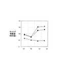
図10は、ゲートラスト構造のNTrにおける工程ごとの移動度の相対変化をゲートピッチに対してプロットした結果を示す。図中、(a)はストレスライナー膜形成後、(b)はゲート電極上のストレスライナー膜の除去後、(c)はポリシリコン層除去後、(d)は金属のゲート電極形成後を示している。相対的な移動度はストレスライナー膜がない場合を1.0としている。
ゲートピッチが長い(0.83μm,0.5μm)場合には、(c)で示されるポリシリコン層除去後に相対的に移動度が増加するが、ゲート電極間が短い(0.19μm)場合にはポリシリコン層除去後に、相対的に移動度が劣化する。
これは、前述したようにNTrではSxxの係数とSyyの係数が同程度で移動度への効果は相殺するよう作用する状態であり、ゲートピッチが短くなるとSxxが相対的に小さくなり、移動度が劣化するためである。
従って、半導体装置の微細化によりゲート間距離が小さくなるに従い、NTrの特性はゲートファースト構造に比較してゲートラスト構造の方が劣化してくるようになることが分かる。FIG. 10 shows a result of plotting the relative change in mobility for each process in the NTr having the gate last structure with respect to the gate pitch. In the figure, (a) is after the stress liner film is formed, (b) is after the stress liner film on the gate electrode is removed, (c) is after the polysilicon layer is removed, and (d) is after the metal gate electrode is formed. ing. The relative mobility is 1.0 when there is no stress liner film.
When the gate pitch is long (0.83 μm, 0.5 μm), the mobility increases relatively after removal of the polysilicon layer shown in (c), but when the distance between the gate electrodes is short (0.19 μm). The mobility is relatively degraded after the removal of the polysilicon layer.
As described above, in NTr, the coefficient of Sxx and the coefficient of Syy are about the same, and the effect on the mobility is canceled out. When the gate pitch is shortened, Sxx becomes relatively small. This is because the mobility deteriorates.
Therefore, it can be understood that the characteristics of the NTr deteriorate in the gate last structure as compared with the gate first structure as the distance between the gates becomes smaller due to miniaturization of the semiconductor device.
上記の特許文献3には、NTrのみゲートファースト構造とする技術が開示されている。
しかし、特許文献3の構造では、PTrにおいてポリシリコン層除去という工程がないため、NTrの移動度の劣化は抑制できても、PTrの移動度の増加もないため、高性能なCMOS回路は得られない。Patent Document 3 discloses a technique in which only NTr has a gate-first structure.
However, in the structure of Patent Document 3, since there is no process of removing the polysilicon layer in the PTr, the deterioration of the mobility of the NTr can be suppressed, and the mobility of the PTr is not increased, so that a high-performance CMOS circuit can be obtained. I can't.
また、例えば非特許文献6に、ゲート絶縁膜に高誘電体膜を用い、ゲート電極に金属材料を用いる方法に関する記載がある。
非特許文献6に開示されたCMOS構造は、NTrはゲートファースト構造、PTrはゲートラスト構造となっているが、NTrにおいてストレスライナー膜の上部を化学機械研磨処理で除去し、ポリシリコン層を除去するという工程を有する。このため、NTrの移動度の劣化が生じ、特にゲート電極間が短い微細領域においては高性能なCMOS回路が得られない。For example, Non-Patent Document 6 describes a method using a high dielectric film for the gate insulating film and a metal material for the gate electrode.
In the CMOS structure disclosed in Non-Patent Document 6, the NTr has a gate first structure and the PTr has a gate last structure. In the NTr, the upper part of the stress liner film is removed by a chemical mechanical polishing process, and the polysilicon layer is removed. It has the process of doing. For this reason, the mobility of NTr is deteriorated, and a high-performance CMOS circuit cannot be obtained particularly in a fine region where the distance between the gate electrodes is short.
解決しようとする課題は、CMOS回路を構成するnチャネルMISFET(NTr)とpチャネルMISFET(PTr)の両者において、キャリア移動度を高めて特にゲート電極間が短い微細領域においても高い性能を実現することが困難であることである。 The problem to be solved is to increase the carrier mobility in both the n-channel MISFET (NTr) and the p-channel MISFET (PTr) constituting the CMOS circuit, and realize high performance even in a fine region where the distance between the gate electrodes is short. It is difficult.
本発明の半導体装置の製造方法は、活性領域における半導体基板のnチャネル電界効果トランジスタ形成領域である第1領域及びpチャネル電界効果トランジスタ形成領域である第2領域において前記半導体基板上に第1ゲート絶縁膜を形成する工程と、前記第1領域及び前記第2領域において前記第1ゲート絶縁膜上に第1ゲート電極を形成する工程と、前記第1領域及び前記第2領域において前記第1ゲート電極の両側部における前記半導体基板中に導電性不純物を導入してソースドレイン領域を形成する工程と、前記ソースドレイン領域の導電性不純物を活性化する熱処理を行う工程と、前記第1領域及び前記第2領域において前記第1ゲート電極を被覆して全面に前記半導体基板に応力を印加するストレスライナー膜を形成する工程と、少なくとも前記第1領域に形成された部分の前記ストレスライナー膜は残しながら前記第2領域における前記第1ゲート電極の上部部分の前記ストレスライナー膜を除去し、前記第2領域における前記第1ゲート電極の上部を露出させる工程と、前記第2領域における前記第1ゲート電極を全て除去して第2ゲート電極形成用溝を形成する工程と、前記第2ゲート電極形成用溝内に第2ゲート電極を形成する工程とを有する。 The semiconductor device manufacturing method of the present invention includes a first gate on the semiconductor substrate in a first region that is an n-channel field effect transistor formation region and a second region that is a p-channel field effect transistor formation region of a semiconductor substrate in an active region. Forming an insulating film; forming a first gate electrode on the first gate insulating film in the first region and the second region; and forming the first gate in the first region and the second region. Introducing a conductive impurity into the semiconductor substrate on both sides of the electrode to form a source / drain region, performing a heat treatment for activating the conductive impurity in the source / drain region, the first region, Forming a stress liner film that covers the first gate electrode and applies stress to the semiconductor substrate over the entire surface in the second region; Removing the stress liner film in the upper portion of the first gate electrode in the second region while leaving at least the portion of the stress liner film formed in the first region, and the first gate in the second region. Exposing the upper portion of the electrode; removing all of the first gate electrode in the second region to form a second gate electrode forming groove; and a second gate in the second gate electrode forming groove. Forming an electrode.
上記の本発明の半導体装置の製造方法は、活性領域における半導体基板のnチャネル電界効果トランジスタ形成領域である第1領域及びpチャネル電界効果トランジスタ形成領域である第2領域において半導体基板上に第1ゲート絶縁膜を形成する。
次に、第1領域及び第2領域において第1ゲート絶縁膜上に第1ゲート電極を形成する。
次に、第1領域及び第2領域において第1ゲート電極の両側部における半導体基板中に導電性不純物を導入してソースドレイン領域を形成する。
次に、ソースドレイン領域の導電性不純物を活性化する熱処理を行う。
次に、第1領域及び第2領域において第1ゲート電極を被覆して全面に半導体基板に応力を印加するストレスライナー膜を形成する。
次に、少なくとも第1領域に形成された部分のストレスライナー膜は残しながら第2領域における第1ゲート電極の上部部分のストレスライナー膜を除去し、第2領域における第1ゲート電極の上部を露出させる。
次に、第2領域における第1ゲート電極を全て除去して第2ゲート電極形成用溝を形成する。
次に、第2ゲート電極形成用溝内に第2ゲート電極を形成する。The method for manufacturing a semiconductor device of the present invention described above includes a first region on the semiconductor substrate in the first region which is an n-channel field effect transistor formation region and a second region which is a p-channel field effect transistor formation region of the semiconductor substrate in the active region. A gate insulating film is formed.
Next, a first gate electrode is formed on the first gate insulating film in the first region and the second region.
Next, in the first region and the second region, conductive impurities are introduced into the semiconductor substrate on both sides of the first gate electrode to form source / drain regions.
Next, heat treatment for activating the conductive impurities in the source / drain regions is performed.
Next, a stress liner film for applying stress to the semiconductor substrate is formed on the entire surface by covering the first gate electrode in the first region and the second region.
Next, the stress liner film in the upper part of the first gate electrode in the second region is removed while leaving the stress liner film formed in at least the first region, and the upper part of the first gate electrode in the second region is exposed. Let
Next, the first gate electrode in the second region is entirely removed to form a second gate electrode formation groove.
Next, a second gate electrode is formed in the second gate electrode formation groove.
また、本発明の半導体装置は、活性領域における半導体基板のnチャネル電界効果トランジスタ形成領域である第1領域において前記半導体基板上に形成された第1ゲート絶縁膜と、活性領域における半導体基板のpチャネル電界効果トランジスタ形成領域である第2の領域において前記半導体基板上に形成された第2ゲート絶縁膜と、前記第1領域において前記第1ゲート絶縁膜上に形成された第1ゲート電極と、前記第2の領域において前記第2ゲート絶縁膜上に形成され、前記第2ゲート絶縁膜に接する部分が金属もしくは金属化合物からなる第2ゲート電極と、前記第1領域及び前記第2の領域において前記第1ゲート電極及び前記第2ゲート電極の両側部における前記半導体基板中に導電性不純物を導入して形成されたソースドレイン領域と、前記第1領域において前記第1ゲート電極を全面に被覆し、かつ、前記第2領域における前記第2ゲート電極の上部部分を除く領域を被覆して形成された前記半導体基板に応力を印加するストレスライナー膜とを有する。 The semiconductor device according to the present invention includes a first gate insulating film formed on the semiconductor substrate in a first region which is an n-channel field effect transistor formation region of the semiconductor substrate in the active region, and a p of the semiconductor substrate in the active region. A second gate insulating film formed on the semiconductor substrate in a second region which is a channel field effect transistor forming region; a first gate electrode formed on the first gate insulating film in the first region; A second gate electrode formed on the second gate insulating film in the second region, and a portion in contact with the second gate insulating film made of a metal or a metal compound; and the first region and the second region A source drain formed by introducing conductive impurities into the semiconductor substrate on both sides of the first gate electrode and the second gate electrode. Stress on the semiconductor substrate formed by covering the entire surface of the first gate electrode in the first region and the region excluding the upper portion of the second gate electrode in the second region. And a stress liner film for applying.
上記の本発明の半導体装置は、活性領域における半導体基板のnチャネル電界効果トランジスタ形成領域である第1領域において前記半導体基板上に第1ゲート絶縁膜が形成されている。また、pチャネル電界効果トランジスタ形成領域である第2の領域において半導体基板上に第2ゲート絶縁膜が形成されている。
第1領域において第1ゲート絶縁膜上に第1ゲート電極が形成され、第2の領域において第2ゲート絶縁膜上に、第2ゲート絶縁膜に接する部分が金属もしくは金属化合物からなる第2ゲート電極が形成されている。
第1領域及び第2の領域において第1ゲート電極及び第2ゲート電極の両側部における半導体基板中に導電性不純物が導入されてソースドレイン領域が形成されている。
第1領域において第1ゲート電極を全面に被覆し、かつ、第2領域における第2ゲート電極の上部部分を除く領域を被覆して半導体基板に応力を印加するストレスライナー膜が形成されている。In the semiconductor device of the present invention, the first gate insulating film is formed on the semiconductor substrate in the first region which is the n-channel field effect transistor formation region of the semiconductor substrate in the active region. A second gate insulating film is formed on the semiconductor substrate in the second region which is a p-channel field effect transistor formation region.
The first gate electrode is formed on the first gate insulating film in the first region, and the second gate is formed on the second gate insulating film in the second region and the portion in contact with the second gate insulating film is made of a metal or a metal compound. An electrode is formed.
In the first region and the second region, conductive impurities are introduced into the semiconductor substrate on both sides of the first gate electrode and the second gate electrode to form source / drain regions.
A stress liner film that covers the entire surface of the first gate electrode in the first region and covers the region excluding the upper portion of the second gate electrode in the second region is applied to apply stress to the semiconductor substrate.
本発明の半導体装置の製造方法によれば、CMOS回路を構成するnチャネルMISFET(NTr)とpチャネルMISFET(PTr)の両者において、キャリア移動度を高めて特にゲート電極間が短い微細領域においても高い性能を実現できる。 According to the method for manufacturing a semiconductor device of the present invention, in both the n-channel MISFET (NTr) and the p-channel MISFET (PTr) constituting the CMOS circuit, the carrier mobility is increased, particularly in a fine region where the distance between the gate electrodes is short. High performance can be realized.
本発明の半導体装置は、CMOS回路を構成するnチャネルMISFET(NTr)とpチャネルMISFET(PTr)の両者において、キャリア移動度を高めて特にゲート電極間が短い微細領域においても高い性能を実現できる。 The semiconductor device of the present invention can increase the carrier mobility in both the n-channel MISFET (NTr) and the p-channel MISFET (PTr) constituting the CMOS circuit, and can realize high performance even in a fine region where the distance between the gate electrodes is short. .
以下に、本発明の半導体装置及びその製造方法の実施の形態について、図面を参照して説明する。 Embodiments of a semiconductor device and a manufacturing method thereof according to the present invention will be described below with reference to the drawings.
尚、説明は以下の順序で行う。
1.第1実施形態(基本構成)
2.第1実施形態の変形例
3.第2実施形態(PTrのゲート電極をNTrのゲート電極より高く形成する方法)The description will be given in the following order.
1. First embodiment (basic configuration)
2. 2. Modification of first embodiment Second Embodiment (Method of Forming PTr Gate Electrode Higher than NTr Gate Electrode)
<第1実施形態>
[半導体装置の構造]
図1は本実施形態に係る半導体装置の模式断面図である。
例えば、シリコン基板などからなる半導体基板の第1領域A1及び第2領域A2を区分するように、素子分離溝10aが形成され、STI(shallow trench isolation)素子分離絶縁膜13が形成されている。
第1領域A1はnチャネル電界効果トランジスタ(NTr)形成領域であり、第2領域A2はpチャネル電界効果トランジスタ(PTr)形成領域である。
半導体基板の第1領域A1にp型ウェル10bが形成されており、第2領域A2にn型ウェル10cが形成されている。<First Embodiment>
[Structure of semiconductor device]
FIG. 1 is a schematic cross-sectional view of a semiconductor device according to this embodiment.
For example, an
The first region A1 is an n-channel field effect transistor (NTr) formation region, and the second region A2 is a p-channel field effect transistor (PTr) formation region.
A p-
例えば、第1領域A1のp型ウェル10b領域において、半導体基板上に酸化ハフニウム(HfO2)などからなる第1ゲート絶縁膜15aが形成されている。
第1ゲート絶縁膜15aの上層に窒化チタン(TiN)膜16及びポリシリコン層17の積層体などからなる第1ゲート電極が形成されている。
第1ゲート絶縁膜15aは、他に酸化ハフニウムシリコン(HfSiO)、酸化窒化ハフニウムシリコン(HfSiON)、酸化ジルコニウム(ZrOx)などの酸化シリコンより高い誘電率を有するいわゆるHigh−k(高誘電率)材料を用いることができる。
また、例えば、第1ゲート電極の第1ゲート絶縁膜15aに接する部分は、NTrに適した仕事関数を有する金属または金属化合物からなる膜が用いられ、本実施形態ではTiN膜16が用いられている。
第1ゲート電極の両側部に窒化シリコン膜20、酸化シリコン膜21及び窒化シリコン膜22の積層体からなるサイドウォール絶縁膜が形成されている。For example, in the p-
A first gate electrode made of a laminate of a titanium nitride (TiN)
The first
In addition, for example, a portion made of a metal or a metal compound having a work function suitable for NTr is used for the portion of the first gate electrode that contacts the first
Sidewall insulating films made of a laminate of a
例えば、第1ゲート電極の両側部における半導体基板のp型ウェル10bの表層部において、第1ゲート電極の下方まで至るn型のエクステンション領域18及びn型のソースドレイン領域23が形成されている。
例えば、第1ゲート電極のポリシリコン層17及びソースドレイン領域23の表層部分に、NiSiなどの高融点金属シリサイド層(25,26)がそれぞれ形成されている。
上記のようにして、nチャネル電界効果トランジスタ(NTr)が形成されている。For example, an n-
For example, refractory metal silicide layers (25, 26) such as NiSi are formed on the surface layer portions of the
As described above, an n-channel field effect transistor (NTr) is formed.
例えば、第2領域A2のn型ウェル10c領域において、半導体基板上に酸化ハフニウムなどからなる第2ゲート絶縁膜15bが形成されている。
第2ゲート絶縁膜15bの上層に窒化チタン(TiN)膜31及びアルミニウム(Al)などからなる導電層32の積層体などからなる第2ゲート電極が形成されている。
第2ゲート絶縁膜15bは、他に酸化ハフニウムシリコン(HfSiO)、酸化窒化ハフニウムシリコン(HfSiON)、酸化ジルコニウム(ZrOx)などの酸化シリコンより高い誘電率を有するいわゆるHigh−k(高誘電率)材料を用いることができる。
第1ゲート絶縁膜15aと第2ゲート絶縁膜15bは、必要な誘電率特性などが合致すれば、同一の絶縁材料からなってもよく、本実施形態では同一の絶縁材料である場合を示している。
また、第1ゲート絶縁膜15aと第2ゲート絶縁膜15bは、必要な誘電率特性などに応じて異なる絶縁材料からなってもよく、これについては後述の変形例において説明する。For example, in the n-
A second gate electrode made of a laminated body of a
The second
The first
Further, the first
また、例えば、第2ゲート電極の第2ゲート絶縁膜15bに接する部分は、PTrに適した仕事関数を有する金属または金属化合物からなる膜が用いられる。例えば、上記の窒化チタンの他、ルテニウム(Ru)、炭化タンタル(TaC)などを好ましく用いることができる。
また、例えば、導電層32としては低抵抗の金属を用いることが好ましく、上記のアルミニウムの他、銅(Cu)あるいはタングステン(W)などを好ましく用いることができる。
第2ゲート電極の両側部に窒化シリコン膜20、酸化シリコン膜21及び窒化シリコン膜22の積層体からなるサイドウォール絶縁膜が形成されている。In addition, for example, a film made of a metal or a metal compound having a work function suitable for PTr is used for the portion of the second gate electrode that contacts the second
For example, it is preferable to use a low-resistance metal as the
Sidewall insulating films made of a laminate of the
上記の第1ゲート絶縁膜及び第2ゲート絶縁膜を高誘電率膜で形成し、さらに第1ゲート電極及び第2ゲート電極のゲート絶縁膜に接する部分に金属もしくは金属化合物を用いることで、実行ゲート酸化膜厚(EOT)を薄膜化することができる。 The first gate insulating film and the second gate insulating film are formed of a high dielectric constant film, and a metal or a metal compound is used for a portion of the first gate electrode and the second gate electrode in contact with the gate insulating film. The gate oxide film thickness (EOT) can be reduced.
例えば、第2ゲート電極の両側部における半導体基板のn型ウェル10cの表層部において、第2ゲート電極の下方まで至るp型のエクステンション領域19及びp型のソースドレイン領域24が形成されている。
例えば、ソースドレイン領域24の表層部分に、NiSiなどの高融点金属シリサイド層26が形成されている。
上記のようにして、pチャネル電界効果トランジスタ(PTr)が形成されている。For example, a p-
For example, a refractory
A p-channel field effect transistor (PTr) is formed as described above.
第1領域A1において、上記のNTrを被覆して全面に窒化シリコンなどからなる第1ストレスライナー膜27が形成されている。
一方、第2領域A2において、上記のPTrを被覆して全面に窒化シリコンなどからなる第2ストレスライナー膜28が形成されている。ここで、第2ストレスライナー膜28は、第2ゲート電極の上部部分を除く領域を被覆して形成されている。In the first region A1, a first
On the other hand, in the second region A2, the second
上記の第1ストレスライナー膜27及び第2ストレスライナー膜28は、それぞれ半導体基板に応力を印加する膜である。
第1ストレスライナー膜27は、NTrの特性を向上させるように半導体基板に応力を印加する特性であることが好ましく、例えば第1ゲート電極のゲート長方向に対して引張応力を半導体基板に印加する膜である。
第2ストレスライナー膜28は、PTrの特性を向上させるように半導体基板に応力を印加する特性であることが好ましく、例えば第2ゲート電極のゲート長方向に対して圧縮応力を半導体基板に印加する膜である。The first
The first
The second
NTrとPTrにそれぞれ異なる応力特性を付与する場合には、上記のように第1領域A1と第2領域A2において応力特性が異なるストレスライナー膜が形成されている構成とする。
応力特性が同一でも良い場合には、共通のストレスライナー膜が形成されていてもよい。When different stress characteristics are imparted to NTr and PTr, stress liner films having different stress characteristics are formed in the first region A1 and the second region A2 as described above.
When the stress characteristics may be the same, a common stress liner film may be formed.
また、第1領域A1と第2領域A2において、第1ストレスライナー膜27及び第2ストレスライナー膜28の上層に酸化シリコンなどからなる第1絶縁膜29が形成されている。
第1絶縁膜29の上層に窒化シリコンなどからなる研磨ストッパ膜30が形成されている。
研磨ストッパ膜30の上層に酸化シリコンなどからなる第2絶縁膜33が形成されている。
第2絶縁膜33、研磨ストッパ膜30及び第1絶縁膜29を貫通して、NTr及びPTrのゲート電極及びソースドレイン領域に達する開口部が形成されており、コンタクトプラグ34が埋め込まれている。さらに、コンタクトプラグ34に接続して、第2絶縁膜33の上層に上層配線35が形成されている。In the first region A1 and the second region A2, a first insulating
A polishing
A second insulating
Openings reaching the gate electrode and source / drain regions of NTr and PTr are formed through the second insulating
NTrは全面にゲート長方向に対して引張応力を付与するストレスライナー膜が形成されたゲートファースト構造のトランジスタであり、上記の引張応力を半導体基板に印加することでNTrのキャリア(電子)の移動度を向上させることができる。
PTrはゲート長方向に対して圧縮応力を付与するストレスライナー膜がゲート上部を除く領域で形成されたゲートラスト構造のトランジスタであり、上記の圧縮応力を半導体基板に印加することでPTrのキャリア(ホール)の移動度を向上させることができる。
上記から、本実施形態の半導体装置は、CMOS回路を構成するnチャネルMISFET(NTr)とpチャネルMISFET(PTr)の両者において、キャリア移動度を高めることができる。特にゲート電極間が短い微細領域においても高い性能を実現できる。NTr is a gate-first structure transistor in which a stress liner film that applies tensile stress to the gate length direction is formed on the entire surface. By applying the tensile stress to a semiconductor substrate, NTr carriers (electrons) move. The degree can be improved.
PTr is a transistor having a gate last structure in which a stress liner film that applies compressive stress to the gate length direction is formed in a region excluding the upper portion of the gate. By applying the compressive stress to the semiconductor substrate, the carrier of PTr ( Hall) mobility can be improved.
From the above, the semiconductor device of this embodiment can increase the carrier mobility in both the n-channel MISFET (NTr) and the p-channel MISFET (PTr) constituting the CMOS circuit. In particular, high performance can be realized even in a fine region between the gate electrodes.
[半導体装置の製造方法]
本実施形態の半導体装置の製造方法について、図2〜5を参照して説明する。
まず、図2(a)に示すように、例えば第1領域A1及び第2領域A2において、ドライ酸化処理などにより半導体基板10上に酸化シリコン膜11を形成し、さらに減圧CVD法などにより窒化シリコン膜12を成膜する。
フォトリソグラフィ工程により第1領域A1及び第2領域A2を保護するパターンのレジスト膜をパターニングする。
次に、レジスト膜をマスクとしてRIE(反応性イオンエッチング)などのエッチング処理を行い、第1領域A1及び第2領域A2以外の酸化シリコン膜11及び窒化シリコン膜12を除去する。
さらに半導体基板10を例えば350〜400nmの深さでエッチングしてSTI用の素子分離溝10aを形成する。
次に、例えば高密度プラズマCVD法などにより素子分離溝10aを埋め込んで650〜700nmの膜厚で酸化シリコン膜を堆積する。高密度プラズマCVD法によれば段差被覆性が良好で緻密な膜を形成することができる。
続いて、STI用溝外部の酸化シリコンを除去して、STI素子分離絶縁膜13を形成する。例えばCMP(化学機械研磨)処理などで窒化シリコン膜12の上面が露出するまで酸化シリコン膜の上面から研磨し、平坦化する。窒化シリコン膜12の形成領域では窒化シリコン膜上の酸化シリコン膜が除去できる程度まで研磨を行う。
また、CMPでのグローバル段差を低減するために、広い活性領域における酸化シリコン膜を、あらかじめリソグラフィパターニング及びエッチング処理で除去することも可能である。
上記のSTI素子分離絶縁膜13の形成領域がフィールド酸化膜領域であり、窒化シリコン膜12が形成された領域が活性領域(第1領域A1及び第2領域A2)である。[Method for Manufacturing Semiconductor Device]
A method for manufacturing the semiconductor device of this embodiment will be described with reference to FIGS.
First, as shown in FIG. 2A, for example, in the first region A1 and the second region A2, a
A resist film having a pattern for protecting the first region A1 and the second region A2 is patterned by a photolithography process.
Next, an etching process such as RIE (reactive ion etching) is performed using the resist film as a mask, and the
Further, the
Next, a silicon oxide film is deposited to a thickness of 650 to 700 nm by filling the
Subsequently, the silicon oxide outside the STI trench is removed, and the STI element
In order to reduce the global level difference in CMP, the silicon oxide film in a wide active region can be removed in advance by lithography patterning and etching.
The region where the STI element
次に、図2(b)に示すように、例えば第1領域A1及び第2領域A2において、熱燐酸により窒化シリコン膜12を除去する。窒化シリコン膜12の除去の前に、STI素子分離絶縁膜13の緻密化や活性領域コーナー部のラウンディング(Rounding)を目的に窒素、酸素、あるいは水素/酸素中でアニールを行ってもよい。
上記において酸化シリコン膜11は実質的に除去されている。ここで、第1領域A1及び第2領域A2において、活性領域表面を例えば10nmの膜厚で酸化処理し、犠牲酸化膜14を形成する。
次に第1領域A1においてイオン注入によりp型ウェル10bを形成する。さらに、パンチスルー阻止を目的とした埋め込み層形成のためのイオン注入やNTrの閾値Vth調整のためのイオン注入が行なわれる。
また、第2領域A2においてイオン注入によりn型ウェル10cを形成する。さらに、パンチスルー阻止を目的とした埋め込み層形成のためのイオン注入やPTrの閾値Vth調整のためのイオン注入が行なわれる。Next, as shown in FIG. 2B, the
In the above, the
Next, the p-
Further, the n-
次に、図2(c)に示すように、例えば第1領域A1及び第2領域A2において、犠牲酸化膜14をHF溶液で剥離し、0.5〜1.5nmの膜厚の界面酸化シリコン膜(不図示)を形成する。
界面酸化シリコン膜の形成方法としてはRTO(Rapid Thermal Oxidization)処理、酸素プラズマ処理、例えば過水系薬液処理による科学的酸化処理などがある。
次に、第1領域A1及び第2領域A2において、例えばCVD(Chemical Vapor Deposition)法あるいはALD(Atomic Layer Deposition)法などにより第1ゲート絶縁膜15a及び第2ゲート絶縁膜15bを2〜3nm程度の膜厚で形成する。
第1ゲート絶縁膜15a及び第2ゲート絶縁膜15bは、酸化ハフニウム(HfO2)、酸化ハフニウムシリコン(HfSiO)、酸化窒化ハフニウムシリコン(HfSiON)、酸化ジルコニウム(ZrOx)などの酸化シリコンより高い誘電率を有するいわゆるHigh−k(高誘電率)材料を用いることができる。
第1ゲート絶縁膜15aと第2ゲート絶縁膜15bは、本実施形態では同一の絶縁材料である場合を示している。Next, as shown in FIG. 2C, for example, in the first region A1 and the second region A2, the
As a method for forming the interfacial silicon oxide film, there is an RTO (Rapid Thermal Oxidization) process, an oxygen plasma process, for example, a scientific oxidation process by a superaqueous chemical process.
Next, in the first region A1 and the second region A2, the first
The first
In this embodiment, the first
次に、第1領域A1及び第2領域A2において、例えばスパッタリング法、CVD法あるいはALD法などによりTiN膜16を5〜20nmの膜厚で形成する。また、トランジスタの閾値Vthを制御するために、TiN膜16の下層に、La、LaOx、AlOxなどからなる薄膜を0.1〜1.0nm程度挿入することも可能である。Next, in the first region A1 and the second region A2, the
次に、第1領域A1及び第2領域A2において、例えばSiH4を原料ガスとし、堆積温度580〜620℃とする減圧CVD法などによりポリシリコン層17を50〜150nmの膜厚で堆積する。
続いてフォトリソグラフィ第1ゲート電極及び第2ゲート電極のパターンのレジスト膜をパターン形成し、HBrあるいはCl系のエッチングガスを用いた異方性エッチングによってゲート電極のパターンに加工する。
これにより、第1領域A1及び第2領域A2で窒化チタン(TiN)膜16及びポリシリコン層17の積層体などからなる第1ゲート電極及び第2ゲート電極がそれぞれ形成される。Next, in the first region A1 and the second region A2, the
Subsequently, a resist film having a pattern of the first gate electrode and the second gate electrode is formed by patterning, and processed into a gate electrode pattern by anisotropic etching using HBr or Cl-based etching gas.
Thereby, a first gate electrode and a second gate electrode made of a laminated body of a titanium nitride (TiN)
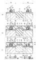
また、この際にレジストパターニング後に酸素プラズマによるトリミング処理などを行うことによってゲート電極パターンを細く形成することも可能であり、例えば32nmノード技術(hp45)ではゲート長を20〜30nm程度で形成することもできる。 At this time, the gate electrode pattern can be formed thin by performing trimming processing using oxygen plasma after resist patterning. For example, in the 32 nm node technology (hp45), the gate length is formed to be about 20 to 30 nm. You can also.
次に、図3(a)に示すように、第1領域A1及び第2領域A2において、例えば減圧CVD法により窒化シリコン膜を5〜15nm程度堆積させ、異方性エッチングによりエッチバックして、サイドウォール絶縁膜を構成する窒化シリコン膜20を形成する。 Next, as shown in FIG. 3A, in the first region A1 and the second region A2, a silicon nitride film is deposited by about 5 to 15 nm by, for example, a low pressure CVD method, and etched back by anisotropic etching. A
次に、第1領域A1において、第1ゲート電極及び窒化シリコン膜20をマスクとしてAs+を5〜10keV、5〜20×1014/cm2でイオン注入してn型のエクステンション領域18を形成する。
また、第1領域A1において、第1ゲート電極及び窒化シリコン膜20をマスクとしてBF2+を3〜5keV、5〜20×1014/cm2でイオン注入してp型のエクステンション領域19を形成する。
オフセットスペーサーである窒化シリコン膜20の形成後に上記イオン注入を行うことによって短チャネル効果を抑制し、トランジスタ特性のばらつきを抑制することが可能である。Next, in the first region A1, using the first gate electrode and the
Further, in the first region A1, the p-
By performing the ion implantation after the formation of the
次に、図3(b)に示すように、第1領域A1及び第2領域A2において、例えばプラズマCVD法により酸化シリコンを10〜30nmの膜厚で堆積して酸化シリコン膜21を形成する。
次に、例えばプラズマCVD法により窒化シリコンを30〜50nmの膜厚で堆積して窒化シリコン膜22を形成する。
次に、異方性エッチングにより酸化シリコン膜21及び窒化シリコン膜22をエッチバックして、上記の窒化シリコン膜20と、酸化シリコン膜21及び窒化シリコン膜22からなるサイドウォール絶縁膜を形成する。Next, as shown in FIG. 3B, in the first region A1 and the second region A2, a
Next,
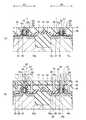
Next, the
次に、図3(c)に示すように、第1領域A1において、第1ゲート電極及びサイドウォール絶縁膜をマスクとしてAs+を40〜50keV、1〜2×10¹⁵/cm2でイオン注入してn型のソースドレイン領域23を形成する。
また、第2領域A2において、第2ゲート電極及びサイドウォール絶縁膜をマスクとしてBF2+を5〜10keV、1〜2×10¹⁵/cm2でイオン注入してp型のソースドレイン領域24を形成する。
次に、例えば1000℃、5秒のRTA処理により不純物の活性化を行う。
また、ドーパント活性化を促進し拡散を抑制する目的のため、スパイクRTA処理で熱処理を行うことも可能である。Next, as shown in FIG. 3C, in the first region A1, using the first gate electrode and the sidewall insulating film as a mask, As+ is ion-implanted at 40 to 50 keV and 1 to 2 × 10¹⁵ / cm2. Thus, the n-type source /
Further, in the second region A2, BF2+ is ion-implanted at 5 to 10 keV and 1 to 2 × 10¹⁵ / cm2 using the second gate electrode and the sidewall insulating film as a mask to form the p-type source /
Next, impurities are activated by, for example, RTA treatment at 1000 ° C. for 5 seconds.
In addition, for the purpose of accelerating dopant activation and suppressing diffusion, heat treatment can be performed by spike RTA treatment.
次に、図4(a)に示すように、第1領域A1及び第2領域A2において、スパッタリング法によりNiなどの高融点金属を6〜8nmの膜厚で堆積し、300〜450℃、10〜60秒のRTA処理を行う。これにより、半導体基板及びゲート電極を構成するポリシリコン層のシリコンと接する部分のみで自己整合的にシリサイド化する。
これにより、第1ゲート電極及び第2ゲート電極のポリシリコン層17とソースドレイン領域(23,24)22の表層部分に、NiSiなどの高融点金属シリサイド層(25,26)をそれぞれ形成する。
次に、H2SO4/H2O2により未反応Niを除去する。
また、Niの代わりにCoやNiPtを堆積することによりCoSi2あるいはNiSiを形成することも可能である。いずれの場合もRTA処理温度は適宜設定することができる。Next, as shown in FIG. 4A, in the first region A1 and the second region A2, a refractory metal such as Ni is deposited with a film thickness of 6 to 8 nm by a sputtering method, and a temperature of 300 to 450.degree. Perform RTA process for ~ 60 seconds. As a result, silicidation is performed in a self-aligned manner only at the portion of the polysilicon layer constituting the semiconductor substrate and the gate electrode that is in contact with silicon.
Thus, refractory metal silicide layers (25, 26) such as NiSi are formed on the
Next, unreacted Ni is removed by H2 SO4 / H2 O2 .
Further, CoSi2 or NiSi can be formed by depositing Co or NiPt instead of Ni. In either case, the RTA treatment temperature can be set as appropriate.
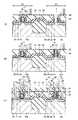
次に、図4(b)に示すように、第1領域A1において、全面に引張応力を有する第1ストレスライナー膜27を形成する。第1ストレスライナー膜として27は、例えばプラズマCVD法によって、30〜50nmの膜厚で1.2GPa程度の引張応力を有する窒化シリコン膜により形成する。
なお、第1ストレスライナー膜27は、以下の条件で化学反応させて成膜可能である。
窒素(N2)ガス:500〜2000cm3/分
アンモニア(NH3)ガス:500〜1500cm3/分
モノシラン(SiH4)ガス:50〜300cm3/分
基板温度:200〜400℃、
圧力:0.67〜2.0kPa
RFパワー:50〜500WNext, as shown in FIG. 4B, a first
The first
Nitrogen(N 2) gas: 500~2000cm3 / min ammonia (NH3) gas: 500~1500cm3 / min monosilane (SiH4) Gas: 50~300cm3 / min substrate temperature: 200 to 400 ° C.,
Pressure: 0.67 to 2.0 kPa
RF power: 50-500W
さらに成膜後、次の条件の紫外線(UV)照射処理を行う。
ヘリウム(He)ガス:10〜20リットル/分
処理温度:400〜600℃
圧力:0.67〜2.0kPa
紫外線(UV)ランプパワー:1〜10kWFurther, after film formation, ultraviolet (UV) irradiation treatment under the following conditions is performed.
Helium (He) gas: 10-20 liters / minute Processing temperature: 400-600 ° C
Pressure: 0.67 to 2.0 kPa
Ultraviolet (UV) lamp power: 1-10kW
その後、フォトリソグラフィ技術およびドライエッチング技術を用いて、第1領域A1のみに上記第1ストレスライナー膜27を残すよう加工する。 Thereafter, using the photolithography technique and the dry etching technique, the first
次に、第2領域A2において、全面に圧縮応力を有する第2ストレスライナー膜28を形成する。第2ストレスライナー膜として28は、例えばプラズマCVD法によって、40nmの膜厚で1.2GPa程度の引張応力を有する窒化シリコン膜により形成する。
なお、第2ストレスライナー膜28は、以下の条件で化学反応させて成膜可能である。
水素(H2)ガス:1000〜5000cm3/分
窒素(N2)ガス:500〜2500cm3/分
アルゴン(Ar)ガス:1000〜5000cm3/分
アンモニア(NH3)ガス:50〜250cm3/分
トリメチルシランモノシランガス:10〜50cm3/分
基板温度:400〜600℃、
圧力:0.13〜0.67kPa
RFパワー:50〜500WNext, a second
The second
Hydrogen(H 2) gas: 1000~5000cm3 / min nitrogen gas(N 2): 500~2500cm3 / min of argon (Ar) gas: 1000~5000cm3 / min ammonia (NH3) gas: 50~250cm3 / Minute Trimethylsilane monosilane gas: 10-50 cm3 / minute Substrate temperature: 400-600 ° C.
Pressure: 0.13-0.67kPa
RF power: 50-500W
その後、フォトリソグラフィ技術およびドライエッチング技術を用いて、第2領域A2のみに上記第2ストレスライナー膜28を残すよう加工する。
本実施形態では、1.2GPaの圧縮応力をもつ膜を形成しているが、応力についてはこの値に限定されるものではない。また膜厚についても本実施例の膜厚に限定されるものではない。
次に、CVD法によって酸化シリコンを500〜1500nmの膜厚で堆積し、CMP処理で平坦化して第1絶縁膜29を形成する。このときストレスライナー膜(27,28)に達するまで研磨を行う。
次に、例えばプラズマCVD法により窒化シリコンを20〜50nm程度堆積し、研磨ストッパ膜30を形成する。Thereafter, using the photolithography technique and the dry etching technique, the second
In the present embodiment, a film having a compressive stress of 1.2 GPa is formed, but the stress is not limited to this value. Further, the film thickness is not limited to the film thickness of this embodiment.
Next, silicon oxide is deposited with a film thickness of 500 to 1500 nm by a CVD method, and planarized by a CMP process to form a first insulating
Next, about 20 to 50 nm of silicon nitride is deposited by plasma CVD, for example, and a polishing
次に、図4(c)に示すように、光リソグラフィにより第2ゲート電極上に開口するようにパターンのレジスト膜(不図示)を形成し、エッチング処理を行う。
このとき、開口領域のパターンは下地である第2ゲート電極のパターンより、線幅や合わせのばらつきを考慮した分、例えば10〜20nm程度大きめに設定する。
開口領域内において、例えばフロロカーボン系のガスなどを用いたドライエッチング処理により、研磨ストッパ膜30及び第2ストレスライナー膜28を除去する。
次に、塩素系のガスなどを用いたドライエッチング処理により、高融点金属シリサイド層25を除去する。
次に、塩素またはHBr系のガスなどを用いたドライエッチング処理により、ポリシリコン層17、TiN膜16を順次除去する。
次に、TiN膜16を除去することも可能であるが、除去しないことも可能である。図面上は除去している。
このようにして、第2ゲート電極形成用溝Tが形成される。Next, as shown in FIG. 4C, a resist film (not shown) having a pattern is formed so as to open on the second gate electrode by photolithography, and an etching process is performed.
At this time, the pattern of the opening region is set larger than the pattern of the second gate electrode which is the base, for example, by about 10 to 20 nm, in consideration of the line width and alignment variation.
In the opening region, the polishing
Next, the refractory
Next, the
Next, the
In this way, the second gate electrode formation trench T is formed.
次に、図5(a)に示すように、第2ゲート電極形成用溝T内において、例えばALD法、スパッタリング法、あるいはCVD法などにより第2ゲート絶縁膜15b上を被覆し、第2ゲート電極形成用溝Tの内壁を被覆して、TiN膜31を10〜30nm膜厚で形成する。
上記の第2ゲート絶縁膜15bに接する部分は、PTrに適した仕事関数を有する金属または金属化合物からなる膜であればよく、TiN膜31の他、ルテニウム(Ru)、炭化タンタル(TaC)などを好ましく用いることができる。
次に、例えばスパッタリング法により第2ゲート電極形成用溝T内を埋め込んでTiN膜31の上層に、アルミニウムなどの導電層32を30〜100nmの膜厚で形成する。
導電層32としては、低抵抗の金属を用いることが好ましく、上記のアルミニウムの他、銅(Cu)あるいはタングステン(W)などを好ましく用いることができる。
次に、研磨ストッパ膜30をストッパとするCMP処理を行い、第2ゲート電極形成用溝Tの外部に堆積されたTiN膜31及び導電層32を除去する。
以上のようにして、TiN膜31及び導電層32の積層体からなり、第2ゲート電極形成用溝Tに埋め込まれたゲートラスト構造の第2ゲート電極が形成される。Next, as shown in FIG. 5A, in the second gate electrode formation trench T, the second
The portion in contact with the second
Next, a
As the
Next, a CMP process using the polishing
As described above, the second gate electrode having the gate last structure, which is composed of the laminated body of the
次に、図5(b)に示すように、例えばCVD法により第1領域A1及び第2領域A2において全面に酸化シリコンを100〜500nmの膜厚で堆積させ、第2絶縁膜33を形成する。
次に、第2絶縁膜33、研磨ストッパ膜30及び第1絶縁膜29を貫通して、NTr及びPTrのゲート電極及びソースドレイン領域に達する開口部を形成し、Ti/TiN及びWを堆積してCMP処理を行い、コンタクトプラグ34を埋め込んで形成する。さらに、コンタクトプラグ34に接続して、第2絶縁膜33の上層に上層配線35を形成する。
Ti/TiN膜の形成方法としてはCVD法の他にIMPを用いたスパッタリング法などの方法で行うことも可能であり、プラグの形成方法として全面エッチバックを用いてもよい。
上層配線35より上層の配線として多層配線を行うことが可能であり、目的に応じて設定することが可能である。また、Alなどの配線を形成することも可能である。Next, as shown in FIG. 5B, a second insulating
Next, an opening reaching the gate electrode and source / drain regions of NTr and PTr is formed through the second insulating
The Ti / TiN film can be formed by a sputtering method using IMP in addition to the CVD method, and the entire surface can be etched back as a plug formation method.
Multilayer wiring can be performed as wiring above the
本実施形態の半導体装置の製造方法によれば、第2ゲート電極上の一部の圧縮応力を有するストレスライナー膜のみを除去する工程では、リソグラフィによるパターニングとエッチングによって膜を除去することが可能である。 According to the semiconductor device manufacturing method of the present embodiment, in the step of removing only the stress liner film having a part of the compressive stress on the second gate electrode, the film can be removed by lithography patterning and etching. is there.
本実施形態の半導体装置の製造方法によれば、CMOS回路を構成するnチャネルMISFET(NTr)とpチャネルMISFET(PTr)の両者において、キャリア移動度を高めて特にゲート電極間が短い微細領域においても高い性能を実現できる。 According to the manufacturing method of the semiconductor device of this embodiment, in both the n-channel MISFET (NTr) and the p-channel MISFET (PTr) constituting the CMOS circuit, the carrier mobility is increased, particularly in a fine region where the distance between the gate electrodes is short. High performance can be achieved.
本実施形態の半導体装置では、第1領域NTr上には連続的に形成された引張応力を有する膜を有し、第2領域のPTrでは圧縮応力を有する膜を有し、かつ第2ゲート電極上部が除去された構造である。
製造工程において、圧縮応力を有する膜を除去した後に第2ゲート電極が置換されたゲートラスト構造である。
NTrではyy方向の圧縮応力Syyを維持し、PTrにはxx方向の応力を効率よく増加させることで、キャリア移動度の高いCMOS回路を実現することが可能である。
引張応力膜や圧縮応力膜をシリコン窒化膜で形成することによって、応力をフレキシブルにコントロールすることが可能である。
また、コンタクトホールのエッチングストッパ膜(Contact Etch Stopper Liner)と兼用することが可能である。
また、第1及び第2ゲート絶縁膜に高誘電体膜を形成し、第2ゲート電極材料の第2ゲート絶縁膜に接する部分に金属もしくは金属化合物を用いることで、実行ゲート酸化膜厚(EOT)を薄膜化しながら、適切な閾値Vthのトランジスタを形成できる。このように、短チャネル効果を抑制したCMOS回路を実現することができる。In the semiconductor device of this embodiment, the first region NTr has a continuously formed film having tensile stress, the second region PTr has a film having compressive stress, and the second gate electrode. The upper part is removed.
In the manufacturing process, the second gate electrode is replaced after the film having compressive stress is removed.
Maintaining the compressive stress Syy of yy direction in NTr, by increasing efficiently xx direction stresses the PTr, it is possible to realize a high carrier mobility CMOS circuit.
By forming the tensile stress film and the compressive stress film with a silicon nitride film, the stress can be controlled flexibly.
It can also be used as a contact hole etching stopper film (Contact Etch Stopper Liner).
Further, a high dielectric film is formed on the first and second gate insulating films, and a metal or a metal compound is used for a portion of the second gate electrode material that is in contact with the second gate insulating film, so that an effective gate oxide film thickness (EOT) is obtained. ), A transistor having an appropriate threshold value Vth can be formed. In this manner, a CMOS circuit that suppresses the short channel effect can be realized.
第1ゲート絶縁膜を形成する工程において、比誘電率が少なくとも8.0より大きな誘電率を持つ絶縁材料により第1ゲート絶縁膜を形成し、第2ゲート電極を形成する工程において、前記第1ゲート絶縁膜に接する部分に金属もしくは金属化合物により第2ゲート電極を形成することが好ましい。これにより、実行ゲート酸化膜厚(EOT)を薄膜化できる。 In the step of forming the first gate insulating film, in the step of forming the first gate insulating film with an insulating material having a dielectric constant greater than at least 8.0 and forming the second gate electrode, The second gate electrode is preferably formed of a metal or a metal compound at a portion in contact with the gate insulating film. Thereby, the effective gate oxide film thickness (EOT) can be reduced.
<変形例>
上記の第1実施形態においては、第1ゲート絶縁膜15aと第2ゲート絶縁膜15bは同一の材料から形成されている。
しかしながら、第1ゲート絶縁膜15aと第2ゲート絶縁膜15bは必要な誘電率特性などに応じて異なる絶縁材料からなってもよい。
本変形例では、第1ゲート絶縁膜15aと第2ゲート絶縁膜15bが異なる材料で形成されている。<Modification>
In the first embodiment, the first
However, the first
In this modification, the first
第1実施形態の図4(c)に示す工程までは、第1実施形態と同様に行う。
次に、図6(a)に示すように、開口領域内において、第2ゲート絶縁膜15bを除去する。
このようにして、第2ゲート電極形成用溝Tが形成される。The steps up to the step shown in FIG. 4C of the first embodiment are performed in the same manner as in the first embodiment.
Next, as shown in FIG. 6A, the second
In this way, the second gate electrode formation trench T is formed.
次に、図6(b)に示すように、例えばCVD(Chemical Vapor Deposition)法あるいはALD(Atomic Layer Deposition)法などにより第2ゲート電極形成用溝Tの少なくとも底面を被覆し、内壁を被覆して第2ゲート絶縁膜36を形成する。 Next, as shown in FIG. 6B, at least the bottom surface of the second gate electrode formation trench T is covered by, for example, a CVD (Chemical Vapor Deposition) method or an ALD (Atomic Layer Deposition) method, and the inner wall is covered. Then, the second
次に、第2ゲート電極形成用溝T内の第2ゲート絶縁膜36上に、例えばALD法、スパッタリング法、あるいはCVD法などによりTiN膜31を10〜30nm膜厚で形成する。
次に、例えばスパッタリング法により第2ゲート電極形成用溝T内を埋め込んでTiN膜31の上層に、アルミニウムなどの導電層32を30〜100nmの膜厚で形成する。
次に、研磨ストッパ膜30をストッパとするCMP処理を行い、第2ゲート電極形成用溝Tの外部に堆積された第2ゲート絶縁膜36、TiN膜31及び導電層32を除去する。
以上のようにして、TiN膜31及び導電層32の積層体からなり、第2ゲート電極形成用溝Tに埋め込まれたゲートラスト構造の第2ゲート電極が形成される。Next, a
Next, a
Next, a CMP process using the polishing
As described above, the second gate electrode having the gate last structure, which is composed of the laminated body of the
次に、図6(c)に示すように、第2絶縁膜33を形成し、NTr及びPTrのゲート電極及びソースドレイン領域に達する開口部を形成し、コンタクトプラグ34及び上層配線35を形成する。 Next, as shown in FIG. 6C, a second insulating
本実施形態の半導体装置の製造方法によれば、CMOS回路を構成するnチャネルMISFET(NTr)とpチャネルMISFET(PTr)の両者において、キャリア移動度を高めて特にゲート電極間が短い微細領域においても高い性能を実現できる。 According to the manufacturing method of the semiconductor device of this embodiment, in both the n-channel MISFET (NTr) and the p-channel MISFET (PTr) constituting the CMOS circuit, the carrier mobility is increased, particularly in a fine region where the distance between the gate electrodes is short. High performance can be achieved.
第2ゲート絶縁膜を形成する工程において、比誘電率が少なくとも8.0より大きな誘電率を持つ絶縁材料により第2ゲート絶縁膜を形成することが好ましい。これにより、実行ゲート酸化膜厚(EOT)を薄膜化できる。 In the step of forming the second gate insulating film, it is preferable that the second gate insulating film is formed of an insulating material having a dielectric constant greater than at least 8.0. Thereby, the effective gate oxide film thickness (EOT) can be reduced.
<第2実施形態>
[半導体装置の構造]
図7は本実施形態に係る半導体装置の模式断面図である。
本実施形態においては、第2ゲート電極が第1実施形態より高く形成されている。また、研磨ストッパ膜が省略されている。
上記を除いて、第1実施形態の半導体装置と同様の構成である。Second Embodiment
[Structure of semiconductor device]
FIG. 7 is a schematic cross-sectional view of the semiconductor device according to the present embodiment.
In the present embodiment, the second gate electrode is formed higher than in the first embodiment. Further, the polishing stopper film is omitted.
Except for the above, the configuration is the same as that of the semiconductor device of the first embodiment.
[半導体装置の製造方法]
第1実施形態の図2(b)に示す工程までは、第1実施形態と同様に行う。
次に、図8(a)に示すように、例えば第2領域A2において、ポリシリコン層17の表面に1〜3nm程度の酸化シリコン膜(不図示)を形成し、例えばポリシリコン層からなる高さ調整層37を30〜100nmの膜厚で形成する。
酸化シリコン膜(不図示)は、熱酸化処理、RTO処理、プラズマ酸化処理などで形成できる。
高さ調整層37は、後述するCMP処理の際にPTr領域のストレスライナー膜のみを研磨するためにNTrの第1ゲート電極との高さを変えるための層である。高さ調整層37は、アモルファスシリコン、酸化シリコン、窒化シリコンなどであってもよい。[Method for Manufacturing Semiconductor Device]
The steps up to the step shown in FIG. 2B of the first embodiment are performed in the same manner as in the first embodiment.
Next, as shown in FIG. 8A, a silicon oxide film (not shown) of about 1 to 3 nm is formed on the surface of the
A silicon oxide film (not shown) can be formed by thermal oxidation treatment, RTO treatment, plasma oxidation treatment, or the like.
The
以降の工程は、実質的に第1実施形態と同様に行う。
即ち、図8(b)に示すように、第1領域A1で窒化チタン(TiN)膜16及びポリシリコン層17の積層体などからなる第1ゲート電極を形成する。
第2領域では、窒化チタン(TiN)膜16、ポリシリコン層17及び高さ調整層37の積層体などからなる第2ゲート電極を形成する。Subsequent steps are performed in substantially the same manner as in the first embodiment.
That is, as shown in FIG. 8B, a first gate electrode made of a laminate of a titanium nitride (TiN)
In the second region, a second gate electrode made of a laminate of a titanium nitride (TiN)
次に、図8(c)に示すように、エクステンション領域(18,19)、窒化シリコン膜20と、酸化シリコン膜21及び窒化シリコン膜22を含むサイドウォール絶縁膜、ソースドレイン領域(23,24)、高融点金属シリサイド層(25,26)を形成する。 Next, as shown in FIG. 8C, the extension region (18, 19), the
次に、図9(a)に示すように、第1領域A1において、全面に引張応力を有する第1ストレスライナー膜27を形成し、第2領域A2において、全面に圧縮応力を有する第2ストレスライナー膜28を形成する。
次に、CVD法によって酸化シリコンを500〜1500nmの膜厚で堆積し、CMP処理で平坦化して第1絶縁膜29を形成する。
このとき、高さ調整層37を除去し、第2領域A2のポリシリコン層17を露出させるまで研磨することにより、PTr領域の第2ストレスライナー膜28のみを研磨除去することができる。Next, as shown in FIG. 9A, a first
Next, silicon oxide is deposited with a film thickness of 500 to 1500 nm by a CVD method, and planarized by a CMP process to form a first insulating
At this time, by removing the
次に、図9(b)に示すように、上記で露出されたポリシリコン層17、TiN膜16を順次除去する。
次に、TiN膜16を除去することも可能であるが、除去しないことも可能である。図面上は除去している。
このようにして、第2ゲート電極形成用溝Tが形成される。Next, as shown in FIG. 9B, the exposed
Next, the
In this way, the second gate electrode formation trench T is formed.
次に、図9(c)に示すように、第2ゲート電極形成用溝T内において、第2ゲート絶縁膜15b上を被覆し、第2ゲート電極形成用溝Tの内壁を被覆して、TiN膜31を形成する。
次に、例えばスパッタリング法により第2ゲート電極形成用溝T内を埋め込んでTiN膜31の上層に導電層32を形成する。
次に、第2ゲート電極形成用溝Tの外部に堆積されたTiN膜31及び導電層32を除去する。
以上のようにして、TiN膜31及び導電層32の積層体からなり、第2ゲート電極形成用溝Tに埋め込まれたゲートラスト構造の第2ゲート電極が形成される。
次に、第2絶縁膜33を形成し、NTr及びPTrのゲート電極及びソースドレイン領域に達する開口部を形成し、コンタクトプラグ34を埋め込んで形成し、上層配線35を形成する。
以上で本実施形態に係る半導体装置を製造することができる。Next, as shown in FIG. 9C, in the second gate electrode formation trench T, the second
Next, the
Next, the
As described above, the second gate electrode having the gate last structure, which is composed of the laminated body of the
Next, a second insulating
The semiconductor device according to the present embodiment can be manufactured as described above.
本実施形態の半導体装置の製造方法によれば、CMOS回路を構成するnチャネルMISFET(NTr)とpチャネルMISFET(PTr)の両者において、キャリア移動度を高めて特にゲート電極間が短い微細領域においても高い性能を実現できる。 According to the manufacturing method of the semiconductor device of this embodiment, in both the n-channel MISFET (NTr) and the p-channel MISFET (PTr) constituting the CMOS circuit, the carrier mobility is increased, particularly in a fine region where the distance between the gate electrodes is short. High performance can be achieved.
本実施形態の半導体装置では、第1領域NTr上には連続的に形成された引張応力を有する膜を有し、第2領域のPTrでは圧縮応力を有する膜を有し、かつ第2ゲート電極上部が除去された構造である。
製造工程において、圧縮応力を有する膜を除去した後に第2ゲート電極が置換されたゲートラスト構造である。
NTrではyy方向の圧縮応力Syyを維持し、PTrにはxx方向の応力を効率よく増加させることで、キャリア移動度の高いCMOS回路を実現することが可能である。
引張応力膜や圧縮応力膜をシリコン窒化膜で形成することによって、応力をフレキシブルにコントロールすることが可能である。
また、コンタクトホールのエッチングストッパ膜(Contact Etch Stopper Liner)と兼用することが可能である。
また、第1及び第2ゲート絶縁膜に高誘電体膜を形成し、第2ゲート電極材料の第2ゲート絶縁膜に接する部分に金属もしくは金属化合物を用いることで、実行ゲート酸化膜厚(EOT)を薄膜化しながら、適切な閾値Vthのトランジスタを形成できる。このように、短チャネル効果を抑制したCMOS回路を実現することができる。In the semiconductor device of this embodiment, the first region NTr has a continuously formed film having tensile stress, the second region PTr has a film having compressive stress, and the second gate electrode. The upper part is removed.
In the manufacturing process, the second gate electrode is replaced after the film having compressive stress is removed.
Maintaining the compressive stress Syy of yy direction in NTr, by increasing efficiently xx direction stresses the PTr, it is possible to realize a high carrier mobility CMOS circuit.
By forming the tensile stress film and the compressive stress film with a silicon nitride film, the stress can be controlled flexibly.
It can also be used as a contact hole etching stopper film (Contact Etch Stopper Liner).
Further, a high dielectric film is formed on the first and second gate insulating films, and a metal or a metal compound is used for a portion of the second gate electrode material that is in contact with the second gate insulating film, so that an effective gate oxide film thickness (EOT) is obtained. ), A transistor having an appropriate threshold value Vth can be formed. In this manner, a CMOS circuit that suppresses the short channel effect can be realized.
上記のように、第2ゲート電極上の一部の圧縮応力を有する膜のみを除去する工程で、CMP処理によって膜を除去することも可能である。
あらかじめ高さの高い領域を形成しておけば、自己整合(Self-Aligned)で除去することが可能である。As described above, in the step of removing only a part of the film having compressive stress on the second gate electrode, the film can be removed by CMP treatment.
If a region having a high height is formed in advance, it can be removed by self-aligned.
本発明は上記の説明に限定されない。
例えば、実施形態においてはNTrとPTrで異なる種類のストレスライナー膜を形成しているが、これに限らず、NTrとPTrで共通のストレスライナー膜を有する構成であってもよい。
第2実施形態において、第1実施形態の変形例と同様に第2ゲート絶縁膜まで除去し、高誘電率の第2ゲート絶縁膜を形成するようにしてもよい。
その他、本発明の要旨を逸脱しない範囲で、種々の変更が可能である。The present invention is not limited to the above description.
For example, in the embodiment, different types of stress liner films are formed for NTr and PTr. However, the present invention is not limited to this, and a configuration having a common stress liner film for NTr and PTr may be used.
In the second embodiment, similarly to the modification of the first embodiment, the second gate insulating film may be removed to form a second gate insulating film having a high dielectric constant.
In addition, various modifications can be made without departing from the scope of the present invention.
10…半導体基板、10a…素子分離溝、10b…p型ウェル、10c…n型ウェル、11…酸化シリコン膜、12…窒化シリコン膜、13…STI素子分離絶縁膜、14…犠牲酸化膜、15a…第1ゲート絶縁膜、15b…第2ゲート絶縁膜、16…TiN膜、17…ポリシリコン層膜、18,19…エクステンション領域、20…窒化シリコン膜、21…酸化シリコン膜、22…窒化シリコン膜、23,24…ソースドレイン領域、25,26…高融点金属シリサイド層、27…第1ストレスライナー膜、28…第2ストレスライナー膜、29…第1絶縁膜、30…研磨ストッパ膜、31…TiN膜、32…導電層、33…第2絶縁膜、34…コンタクトプラグ、35…上層配線、36…第2ゲート絶縁膜、37…高さ調整層、A1…第1領域、A2…第2領域、NTr…nチャネルMISFET、PTr…pチャネルMISFET DESCRIPTION OF
Claims (10)
Translated fromJapanese前記第1領域及び前記第2領域において前記第1ゲート絶縁膜上に第1ゲート電極を形成する工程と、
前記第1領域及び前記第2領域において前記第1ゲート電極の両側部における前記半導体基板中に導電性不純物を導入してソースドレイン領域を形成する工程と、
前記ソースドレイン領域の導電性不純物を活性化する熱処理を行う工程と、
前記第1領域及び前記第2領域において前記第1ゲート電極を被覆して全面に前記半導体基板に応力を印加するストレスライナー膜を形成する工程と、
少なくとも前記第1領域に形成された部分の前記ストレスライナー膜は残しながら前記第2領域における前記第1ゲート電極の上部部分の前記ストレスライナー膜を除去し、前記第2領域における前記第1ゲート電極の上部を露出させる工程と、
前記第2領域における前記第1ゲート電極を全て除去して第2ゲート電極形成用溝を形成する工程と、
前記第2ゲート電極形成用溝内に第2ゲート電極を形成する工程と
を有する半導体装置の製造方法。Forming a first gate insulating film on the semiconductor substrate in a first region that is an n-channel field effect transistor formation region and a second region that is a p-channel field effect transistor formation region of the semiconductor substrate in the active region;
Forming a first gate electrode on the first gate insulating film in the first region and the second region;
Forming a source / drain region by introducing conductive impurities into the semiconductor substrate on both sides of the first gate electrode in the first region and the second region;
Performing a heat treatment for activating the conductive impurities in the source / drain region;
Forming a stress liner film that covers the first gate electrode in the first region and the second region and applies stress to the semiconductor substrate over the entire surface;
The stress liner film in the upper portion of the first gate electrode in the second region is removed while leaving at least the portion of the stress liner film formed in the first region, and the first gate electrode in the second region is removed. Exposing the top of the
Removing all of the first gate electrode in the second region to form a second gate electrode formation groove;
Forming a second gate electrode in the groove for forming the second gate electrode.
請求項1に記載の半導体装置の製造方法。The step of forming the stress liner film forms a first stress liner film in the first region, and forms a second stress liner film having a stress characteristic different from that of the first stress liner film in the second region. Item 14. A method for manufacturing a semiconductor device according to Item 1.
前記第2ストレスライナー膜を形成する工程において、前記第1ゲート電極のゲート長方向に対して圧縮応力を前記半導体基板に印加するストレスライナー膜を形成する
請求項2に記載の半導体装置の製造方法。In the step of forming the first stress liner film, a stress liner film for applying a tensile stress to the semiconductor substrate with respect to the gate length direction of the first gate electrode is formed.
3. The method of manufacturing a semiconductor device according to claim 2, wherein in the step of forming the second stress liner film, a stress liner film that applies compressive stress to the semiconductor substrate in a gate length direction of the first gate electrode is formed. .
請求項1に記載の半導体装置の製造方法。The step of removing the stress liner film on the upper part of the first gate electrode in the second region and exposing the upper part of the first gate electrode in the second region includes the step of exposing the first gate electrode in the second region. The method includes: forming a resist film having a pattern opening an upper portion of the first region; and removing the stress liner film on the upper portion of the first gate electrode in the second region using the resist film as a mask. The manufacturing method of the semiconductor device of description.
前記第2領域における前記第1ゲート電極の上部部分の前記ストレスライナー膜を除去し、前記第2領域における前記第1ゲート電極の上部を露出させる工程が、前記第2領域の前記第1ゲート電極の少なくとも上部まで除去するように前記ストレスライナー膜の上方から研磨処理する工程を含む
請求項1に記載の半導体装置の製造方法。In the step of forming the first gate electrode on the first gate insulating film in the first region and the second region, the second region is thicker than the first region as the first gate electrode. 1 gate electrode is formed,
The step of removing the stress liner film on the upper portion of the first gate electrode in the second region and exposing the upper portion of the first gate electrode in the second region includes the step of exposing the first gate electrode in the second region. The method for manufacturing a semiconductor device according to claim 1, further comprising a polishing process from above the stress liner film so as to remove at least an upper portion of the stress liner film.
請求項1に記載の半導体装置の製造方法。The method of manufacturing a semiconductor device according to claim 1, wherein in the step of forming a second gate electrode in the second gate electrode formation groove, the second gate electrode is formed on an upper layer of the first gate insulating film.
前記第2ゲート電極形成用溝内に第2ゲート電極を形成する工程において、前記第2ゲート絶縁膜の上層に前記第2ゲート電極を形成する
請求項1に記載の半導体装置の製造方法。Between the step of removing the first gate electrode in the second region to form a second gate electrode formation groove and the step of forming a second gate electrode in the second gate electrode formation groove, Removing the first gate insulating film in the second gate electrode forming groove; and forming a second gate insulating film by covering at least the bottom of the second gate electrode forming groove;
The method of manufacturing a semiconductor device according to claim 1, wherein in the step of forming the second gate electrode in the second gate electrode formation groove, the second gate electrode is formed in an upper layer of the second gate insulating film.
請求項1記載の半導体装置の製造方法。In the step of forming thepre-Symbol stress liner film, method of manufacturing a semiconductor device according to claim 1, wherein forming the silicon nitride film as the stress liner film.
前記第2ゲート電極を形成する工程において、前記第1ゲート絶縁膜に接する部分に金属もしくは金属化合物により第2ゲート電極を形成する
請求項1記載の半導体装置の製造方法。In the step of forming the first gate insulating film, the first gate insulating film is formed of an insulating material having a dielectric constant greater than at least 8.0.
The method for manufacturing a semiconductor device according to claim 1, wherein in the step of forming the second gate electrode, the second gate electrode is formed of a metal or a metal compound in a portion in contact with the first gate insulating film.
請求項7記載の半導体装置の製造方法。The method for manufacturing a semiconductor device according to claim 7, wherein in the step of forming the second gate insulating film, the second gate insulating film is formed of an insulating material having a dielectric constant greater than at least 8.0.
Priority Applications (4)
| Application Number | Priority Date | Filing Date | Title |
|---|---|---|---|
| JP2010139847AJP5569173B2 (en) | 2010-06-18 | 2010-06-18 | Semiconductor device manufacturing method and semiconductor device |
| TW100118366ATWI469262B (en) | 2010-06-18 | 2011-05-25 | Semiconductor device manufacturing method and semiconductor device |
| US13/116,727US8871585B2 (en) | 2010-06-18 | 2011-05-26 | Manufacturing method of semiconductor device and semiconductor device |
| CN2011101568418ACN102290375A (en) | 2010-06-18 | 2011-06-10 | Semiconductor device and manufacturing method thereof |
Applications Claiming Priority (1)
| Application Number | Priority Date | Filing Date | Title |
|---|---|---|---|
| JP2010139847AJP5569173B2 (en) | 2010-06-18 | 2010-06-18 | Semiconductor device manufacturing method and semiconductor device |
Publications (2)
| Publication Number | Publication Date |
|---|---|
| JP2012004455A JP2012004455A (en) | 2012-01-05 |
| JP5569173B2true JP5569173B2 (en) | 2014-08-13 |
Family
ID=45327910
Family Applications (1)
| Application Number | Title | Priority Date | Filing Date |
|---|---|---|---|
| JP2010139847AExpired - Fee RelatedJP5569173B2 (en) | 2010-06-18 | 2010-06-18 | Semiconductor device manufacturing method and semiconductor device |
Country Status (4)
| Country | Link |
|---|---|
| US (1) | US8871585B2 (en) |
| JP (1) | JP5569173B2 (en) |
| CN (1) | CN102290375A (en) |
| TW (1) | TWI469262B (en) |
Families Citing this family (11)
| Publication number | Priority date | Publication date | Assignee | Title |
|---|---|---|---|---|
| US8466513B2 (en) | 2011-06-13 | 2013-06-18 | Semiconductor Components Industries, Llc | Semiconductor device with enhanced mobility and method |
| JP5837387B2 (en)* | 2011-10-11 | 2015-12-24 | ルネサスエレクトロニクス株式会社 | Semiconductor integrated circuit device and method for manufacturing semiconductor integrated circuit device |
| JP5798502B2 (en)* | 2012-01-31 | 2015-10-21 | ルネサスエレクトロニクス株式会社 | Semiconductor device and manufacturing method thereof |
| JP5888064B2 (en)* | 2012-03-29 | 2016-03-16 | 富士通株式会社 | Compound semiconductor device and manufacturing method thereof |
| CN103378003A (en)* | 2012-04-23 | 2013-10-30 | 中芯国际集成电路制造(上海)有限公司 | Method for manufacturing CMOS device by means of stress memorization technique |
| KR101742556B1 (en) | 2012-11-02 | 2017-06-01 | 캐논 아네르바 가부시키가이샤 | Method for manufacturing semiconductor device, ion beam etching device, and control device |
| US8946793B2 (en)* | 2013-02-05 | 2015-02-03 | GlobalFoundries, Inc. | Integrated circuits having replacement gate structures and methods for fabricating the same |
| JP6085803B2 (en)* | 2013-02-19 | 2017-03-01 | 富士通セミコンダクター株式会社 | Manufacturing method of semiconductor device |
| US9722076B2 (en) | 2015-08-29 | 2017-08-01 | Taiwan Semiconductor Manufacturning Co., Ltd. | Method for manufacturing semiconductor device with contamination improvement |
| KR102487549B1 (en)* | 2017-11-23 | 2023-01-11 | 삼성전자주식회사 | Semiconductor device having transistors |
| US10957589B2 (en) | 2017-11-30 | 2021-03-23 | Mediatek Inc. | Self-aligned contact and method for forming the same |
Family Cites Families (14)
| Publication number | Priority date | Publication date | Assignee | Title |
|---|---|---|---|---|
| JP3142125B2 (en) | 1999-07-16 | 2001-03-07 | 株式会社東芝 | Semiconductor device |
| JP2002198441A (en)* | 2000-11-16 | 2002-07-12 | Hynix Semiconductor Inc | Method of forming dual metal gate for semiconductor device |
| CN1449585A (en) | 2000-11-22 | 2003-10-15 | 株式会社日立制作所 | Semiconductor device and manufacturing method thereof |
| JP2005303261A (en)* | 2004-03-19 | 2005-10-27 | Nec Electronics Corp | Semiconductor device and manufacturing method therefor |
| JP2006351581A (en)* | 2005-06-13 | 2006-12-28 | Fujitsu Ltd | Manufacturing method of semiconductor device |
| WO2007122667A1 (en)* | 2006-03-29 | 2007-11-01 | Fujitsu Limited | Semiconductor device and its manufacturing method |
| TWI346361B (en)* | 2006-10-04 | 2011-08-01 | United Microelectronics Corp | Method for fabricating high compressive stress film and strained-silicon transistors |
| JP2008117963A (en)* | 2006-11-06 | 2008-05-22 | Nec Electronics Corp | Field effect transistor, semiconductor device, and manufacturing method thereof |
| JP5003515B2 (en)* | 2007-03-20 | 2012-08-15 | ソニー株式会社 | Semiconductor device |
| DE102007041207B4 (en)* | 2007-08-31 | 2015-05-21 | Globalfoundries Dresden Module One Limited Liability Company & Co. Kg | CMOS device with gate insulation layers of different type and thickness and method of manufacture |
| JP2009117621A (en)* | 2007-11-07 | 2009-05-28 | Panasonic Corp | Semiconductor device and manufacturing method thereof |
| JP2009198441A (en) | 2008-02-25 | 2009-09-03 | Nec Corp | Device and method for searching target |
| JP4770885B2 (en)* | 2008-06-30 | 2011-09-14 | ソニー株式会社 | Semiconductor device |
| US8084824B2 (en)* | 2008-09-11 | 2011-12-27 | United Microelectronics Corp. | Metal gate transistor and method for fabricating the same |
- 2010
- 2010-06-18JPJP2010139847Apatent/JP5569173B2/ennot_activeExpired - Fee Related
- 2011
- 2011-05-25TWTW100118366Apatent/TWI469262B/ennot_activeIP Right Cessation
- 2011-05-26USUS13/116,727patent/US8871585B2/ennot_activeExpired - Fee Related
- 2011-06-10CNCN2011101568418Apatent/CN102290375A/enactivePending
Also Published As
| Publication number | Publication date |
|---|---|
| TWI469262B (en) | 2015-01-11 |
| US20110309451A1 (en) | 2011-12-22 |
| US8871585B2 (en) | 2014-10-28 |
| CN102290375A (en) | 2011-12-21 |
| JP2012004455A (en) | 2012-01-05 |
| TW201208001A (en) | 2012-02-16 |
Similar Documents
| Publication | Publication Date | Title |
|---|---|---|
| US11121133B2 (en) | Semiconductor device with fin transistors and manufacturing method of such semiconductor device | |
| JP5569173B2 (en) | Semiconductor device manufacturing method and semiconductor device | |
| KR101027107B1 (en) | Metal gate MOSPFET by fully converted semiconductor metal alloy | |
| US9397009B2 (en) | Structure and method for metal gate stack oxygen concentration control using an oxygen diffusion barrier layer and a sacrificial oxygen gettering layer | |
| JP5326274B2 (en) | Semiconductor device and manufacturing method of semiconductor device | |
| US7381619B2 (en) | Dual work-function metal gates | |
| US8728908B2 (en) | Methods of forming a dielectric cap layer on a metal gate structure | |
| US20120045876A1 (en) | Method for manufacturing a semiconductor device | |
| US9076857B2 (en) | Semiconductor device and manufacturing method thereof | |
| US20090057786A1 (en) | Semiconductor device and method of manufacturing semiconductor device | |
| US8471341B2 (en) | Semiconductor device and method for fabricating the same | |
| US9218975B2 (en) | Methods of forming a replacement gate structure having a gate electrode comprised of a deposited intermetallic compound material | |
| TW202447868A (en) | Integrated circuit structure and forming method thereof | |
| JP2010021363A (en) | Semiconductor device and method of producing the same | |
| TWI509702B (en) | Metal gate transistor and method for fabricating the same | |
| TWI859921B (en) | Semiconductor device and manufacturing method thereof | |
| JP4145272B2 (en) | Manufacturing method of semiconductor device | |
| JP2008277420A (en) | Semiconductor device and manufacturing method thereof |
Legal Events
| Date | Code | Title | Description |
|---|---|---|---|
| A621 | Written request for application examination | Free format text:JAPANESE INTERMEDIATE CODE: A621 Effective date:20130430 | |
| A131 | Notification of reasons for refusal | Free format text:JAPANESE INTERMEDIATE CODE: A131 Effective date:20140225 | |
| A977 | Report on retrieval | Free format text:JAPANESE INTERMEDIATE CODE: A971007 Effective date:20140228 | |
| A521 | Request for written amendment filed | Free format text:JAPANESE INTERMEDIATE CODE: A523 Effective date:20140418 | |
| TRDD | Decision of grant or rejection written | ||
| A01 | Written decision to grant a patent or to grant a registration (utility model) | Free format text:JAPANESE INTERMEDIATE CODE: A01 Effective date:20140527 | |
| A61 | First payment of annual fees (during grant procedure) | Free format text:JAPANESE INTERMEDIATE CODE: A61 Effective date:20140609 | |
| LAPS | Cancellation because of no payment of annual fees |