JP5568291B2 - Multi-pole plug - Google Patents
Multi-pole plugDownload PDFInfo
- Publication number
- JP5568291B2 JP5568291B2JP2009281946AJP2009281946AJP5568291B2JP 5568291 B2JP5568291 B2JP 5568291B2JP 2009281946 AJP2009281946 AJP 2009281946AJP 2009281946 AJP2009281946 AJP 2009281946AJP 5568291 B2JP5568291 B2JP 5568291B2
- Authority
- JP
- Japan
- Prior art keywords
- shell
- plug
- cable
- connector
- side connector
- Prior art date
- Legal status (The legal status is an assumption and is not a legal conclusion. Google has not performed a legal analysis and makes no representation as to the accuracy of the status listed.)
- Active
Links
- 230000005405multipoleEffects0.000titleclaimsdescription10
- 239000002184metalSubstances0.000claimsdescription31
- 230000013011matingEffects0.000claimsdescription23
- 238000005452bendingMethods0.000claimsdescription13
- 239000011810insulating materialSubstances0.000claimsdescription8
- 239000000758substrateSubstances0.000description16
- 230000008054signal transmissionEffects0.000description12
- 238000003780insertionMethods0.000description10
- 230000037431insertionEffects0.000description10
- 238000005476solderingMethods0.000description8
- 238000003825pressingMethods0.000description7
- 238000004080punchingMethods0.000description7
- 238000003860storageMethods0.000description7
- 238000007789sealingMethods0.000description2
- 230000001629suppressionEffects0.000description2
- 239000002131composite materialSubstances0.000description1
- 230000008878couplingEffects0.000description1
- 238000010168coupling processMethods0.000description1
- 238000005859coupling reactionMethods0.000description1
- 238000005520cutting processMethods0.000description1
- 230000002542deteriorative effectEffects0.000description1
- 238000010586diagramMethods0.000description1
- 230000000694effectsEffects0.000description1
- 238000000605extractionMethods0.000description1
- 238000005304joiningMethods0.000description1
- 238000000034methodMethods0.000description1
- 238000012986modificationMethods0.000description1
- 230000004048modificationEffects0.000description1
- 230000036316preloadEffects0.000description1
- 229910000679solderInorganic materials0.000description1
Images


Classifications
- H—ELECTRICITY
- H01—ELECTRIC ELEMENTS
- H01R—ELECTRICALLY-CONDUCTIVE CONNECTIONS; STRUCTURAL ASSOCIATIONS OF A PLURALITY OF MUTUALLY-INSULATED ELECTRICAL CONNECTING ELEMENTS; COUPLING DEVICES; CURRENT COLLECTORS
- H01R13/00—Details of coupling devices of the kinds covered by groups H01R12/70 or H01R24/00 - H01R33/00
- H01R13/646—Details of coupling devices of the kinds covered by groups H01R12/70 or H01R24/00 - H01R33/00 specially adapted for high-frequency, e.g. structures providing an impedance match or phase match
- H01R13/6461—Means for preventing cross-talk
- H—ELECTRICITY
- H01—ELECTRIC ELEMENTS
- H01R—ELECTRICALLY-CONDUCTIVE CONNECTIONS; STRUCTURAL ASSOCIATIONS OF A PLURALITY OF MUTUALLY-INSULATED ELECTRICAL CONNECTING ELEMENTS; COUPLING DEVICES; CURRENT COLLECTORS
- H01R13/00—Details of coupling devices of the kinds covered by groups H01R12/70 or H01R24/00 - H01R33/00
- H01R13/648—Protective earth or shield arrangements on coupling devices, e.g. anti-static shielding
- H01R13/6485—Electrostatic discharge protection
- H—ELECTRICITY
- H01—ELECTRIC ELEMENTS
- H01R—ELECTRICALLY-CONDUCTIVE CONNECTIONS; STRUCTURAL ASSOCIATIONS OF A PLURALITY OF MUTUALLY-INSULATED ELECTRICAL CONNECTING ELEMENTS; COUPLING DEVICES; CURRENT COLLECTORS
- H01R13/00—Details of coupling devices of the kinds covered by groups H01R12/70 or H01R24/00 - H01R33/00
- H01R13/62—Means for facilitating engagement or disengagement of coupling parts or for holding them in engagement
- H01R13/639—Additional means for holding or locking coupling parts together, after engagement, e.g. separate keylock, retainer strap
- H01R13/6392—Additional means for holding or locking coupling parts together, after engagement, e.g. separate keylock, retainer strap for extension cord
- H—ELECTRICITY
- H01—ELECTRIC ELEMENTS
- H01R—ELECTRICALLY-CONDUCTIVE CONNECTIONS; STRUCTURAL ASSOCIATIONS OF A PLURALITY OF MUTUALLY-INSULATED ELECTRICAL CONNECTING ELEMENTS; COUPLING DEVICES; CURRENT COLLECTORS
- H01R13/00—Details of coupling devices of the kinds covered by groups H01R12/70 or H01R24/00 - H01R33/00
- H01R13/62—Means for facilitating engagement or disengagement of coupling parts or for holding them in engagement
- H01R13/639—Additional means for holding or locking coupling parts together, after engagement, e.g. separate keylock, retainer strap
- H01R13/6395—Additional means for holding or locking coupling parts together, after engagement, e.g. separate keylock, retainer strap for wall or panel outlets
- H—ELECTRICITY
- H01—ELECTRIC ELEMENTS
- H01R—ELECTRICALLY-CONDUCTIVE CONNECTIONS; STRUCTURAL ASSOCIATIONS OF A PLURALITY OF MUTUALLY-INSULATED ELECTRICAL CONNECTING ELEMENTS; COUPLING DEVICES; CURRENT COLLECTORS
- H01R13/00—Details of coupling devices of the kinds covered by groups H01R12/70 or H01R24/00 - H01R33/00
- H01R13/62—Means for facilitating engagement or disengagement of coupling parts or for holding them in engagement
- H01R13/639—Additional means for holding or locking coupling parts together, after engagement, e.g. separate keylock, retainer strap
- H01R13/6397—Additional means for holding or locking coupling parts together, after engagement, e.g. separate keylock, retainer strap with means for preventing unauthorised use
- H—ELECTRICITY
- H01—ELECTRIC ELEMENTS
- H01R—ELECTRICALLY-CONDUCTIVE CONNECTIONS; STRUCTURAL ASSOCIATIONS OF A PLURALITY OF MUTUALLY-INSULATED ELECTRICAL CONNECTING ELEMENTS; COUPLING DEVICES; CURRENT COLLECTORS
- H01R13/00—Details of coupling devices of the kinds covered by groups H01R12/70 or H01R24/00 - H01R33/00
- H01R13/64—Means for preventing incorrect coupling
- H01R13/641—Means for preventing incorrect coupling by indicating incorrect coupling; by indicating correct or full engagement
- H—ELECTRICITY
- H01—ELECTRIC ELEMENTS
- H01R—ELECTRICALLY-CONDUCTIVE CONNECTIONS; STRUCTURAL ASSOCIATIONS OF A PLURALITY OF MUTUALLY-INSULATED ELECTRICAL CONNECTING ELEMENTS; COUPLING DEVICES; CURRENT COLLECTORS
- H01R13/00—Details of coupling devices of the kinds covered by groups H01R12/70 or H01R24/00 - H01R33/00
- H01R13/64—Means for preventing incorrect coupling
- H01R13/642—Means for preventing incorrect coupling by position or shape of contact members
- H—ELECTRICITY
- H01—ELECTRIC ELEMENTS
- H01R—ELECTRICALLY-CONDUCTIVE CONNECTIONS; STRUCTURAL ASSOCIATIONS OF A PLURALITY OF MUTUALLY-INSULATED ELECTRICAL CONNECTING ELEMENTS; COUPLING DEVICES; CURRENT COLLECTORS
- H01R13/00—Details of coupling devices of the kinds covered by groups H01R12/70 or H01R24/00 - H01R33/00
- H01R13/648—Protective earth or shield arrangements on coupling devices, e.g. anti-static shielding
- H01R13/658—High frequency shielding arrangements, e.g. against EMI [Electro-Magnetic Interference] or EMP [Electro-Magnetic Pulse]
- H01R13/6581—Shield structure
- H01R13/6582—Shield structure with resilient means for engaging mating connector
- H—ELECTRICITY
- H01—ELECTRIC ELEMENTS
- H01R—ELECTRICALLY-CONDUCTIVE CONNECTIONS; STRUCTURAL ASSOCIATIONS OF A PLURALITY OF MUTUALLY-INSULATED ELECTRICAL CONNECTING ELEMENTS; COUPLING DEVICES; CURRENT COLLECTORS
- H01R13/00—Details of coupling devices of the kinds covered by groups H01R12/70 or H01R24/00 - H01R33/00
- H01R13/648—Protective earth or shield arrangements on coupling devices, e.g. anti-static shielding
- H01R13/658—High frequency shielding arrangements, e.g. against EMI [Electro-Magnetic Interference] or EMP [Electro-Magnetic Pulse]
- H01R13/6591—Specific features or arrangements of connection of shield to conductive members
- H01R13/6592—Specific features or arrangements of connection of shield to conductive members the conductive member being a shielded cable
- H01R13/6593—Specific features or arrangements of connection of shield to conductive members the conductive member being a shielded cable the shield being composed of different pieces
- H—ELECTRICITY
- H01—ELECTRIC ELEMENTS
- H01R—ELECTRICALLY-CONDUCTIVE CONNECTIONS; STRUCTURAL ASSOCIATIONS OF A PLURALITY OF MUTUALLY-INSULATED ELECTRICAL CONNECTING ELEMENTS; COUPLING DEVICES; CURRENT COLLECTORS
- H01R13/00—Details of coupling devices of the kinds covered by groups H01R12/70 or H01R24/00 - H01R33/00
- H01R13/648—Protective earth or shield arrangements on coupling devices, e.g. anti-static shielding
- H01R13/658—High frequency shielding arrangements, e.g. against EMI [Electro-Magnetic Interference] or EMP [Electro-Magnetic Pulse]
- H01R13/6591—Specific features or arrangements of connection of shield to conductive members
- H01R13/6594—Specific features or arrangements of connection of shield to conductive members the shield being mounted on a PCB and connected to conductive members
- H—ELECTRICITY
- H01—ELECTRIC ELEMENTS
- H01R—ELECTRICALLY-CONDUCTIVE CONNECTIONS; STRUCTURAL ASSOCIATIONS OF A PLURALITY OF MUTUALLY-INSULATED ELECTRICAL CONNECTING ELEMENTS; COUPLING DEVICES; CURRENT COLLECTORS
- H01R2107/00—Four or more poles
- H—ELECTRICITY
- H01—ELECTRIC ELEMENTS
- H01R—ELECTRICALLY-CONDUCTIVE CONNECTIONS; STRUCTURAL ASSOCIATIONS OF A PLURALITY OF MUTUALLY-INSULATED ELECTRICAL CONNECTING ELEMENTS; COUPLING DEVICES; CURRENT COLLECTORS
- H01R43/00—Apparatus or processes specially adapted for manufacturing, assembling, maintaining, or repairing of line connectors or current collectors or for joining electric conductors
- H01R43/16—Apparatus or processes specially adapted for manufacturing, assembling, maintaining, or repairing of line connectors or current collectors or for joining electric conductors for manufacturing contact members, e.g. by punching and by bending
Landscapes
- Engineering & Computer Science (AREA)
- Computer Security & Cryptography (AREA)
- Details Of Connecting Devices For Male And Female Coupling (AREA)
Description
Translated fromJapanese本発明は、EMI(Electro Magenetic Interferrence:電磁妨害)対策としてのシールドを備えた多極プラグに関する。 The present invention relates to a multipolar plug having a shield as a measure against EMI (Electro Magenetic Interferrence).
従来、多極雄型コネクタ(多極プラグ)としてのケーブル側コネクタと、その嵌合相手の多極雌型コネクタ(多極レセプタクル)としての基板実装側(機器側)コネクタ、それぞれの嵌合部の周囲の覆いとしてのシェルを金属板によって形成し、シェルにシールド性を持たせ、ケーブル側コネクタと基板実装側コネクタを嵌合した際にシェル同士が電気的に結合するようにする多極コネクタのEMI対策がある。シェルは多極コネクタのコストダウンと小型化を図ることを目的として金属板の打ち抜き加工及び曲げ加工等のプレス加工によって筒状に形成されるため継ぎ目を有し、その継ぎ目はシェルの強度バランスを保つことを目的としてシェルの中心線を中心に形成されていた(特許文献1参照)。 Conventionally, the cable side connector as a multi-pole male connector (multi-pole plug) and the board mounting side (equipment side) connector as the mating counterpart multi-pole female connector (multi-pole receptacle), each fitting part A multi-pole connector that forms a shell as a cover around the metal plate, has a shielding property for the shell, and electrically connects the shells when the cable side connector and the board mounting side connector are fitted together There are EMI countermeasures. The shell has a seam because it is formed into a cylindrical shape by stamping and bending of a metal plate for the purpose of reducing the cost and miniaturization of the multipolar connector, and the seam has a strength balance of the shell. It was formed around the center line of the shell for the purpose of maintaining (see Patent Document 1).
前記従来技術では、ケーブル側コネクタと基板実装側コネクタを嵌合した際にシェルの継ぎ目が一致し、その一致した継ぎ目の隙間より高周波ノイズが漏れるおそれがある。 In the prior art, when the cable side connector and the board mounting side connector are fitted, the seams of the shells coincide with each other, and high-frequency noise may leak from the gaps of the coincident seams.
本発明は、このような問題に鑑みてなされたもので、多極コネクタのEMI特性を改善する多極プラグを提供することを目的とする。 The present invention has been made in view of such a problem, and an object thereof is to provide a multipolar plug that improves the EMI characteristics of a multipolar connector.
前述した課題を解決するため本発明に係る多極プラグは、相手コネクタが、多極プラグとの嵌合部の周囲の覆いとしての筒状のレセプタクル側シェルを備え、このレセプタクル側シェルが金属板の曲げ加工によって形成されてシールド性を持つと共に前記金属板の両端面が突き合わされた継ぎ目を有し、絶縁材料からなるレセプタクル側ボディに装着された複数本のレセプタクル側コンタクトが、前記レセプタクル側シェルの内側に設けられ、高速差動信号用の複数組のレセプタクル側コンタクト対を含んだ多極レセプタクルであって、
前記相手コネクタへの嵌合部の周囲の覆いとしての筒状のプラグ側シェルを備え、このプラグ側シェルが金属板の曲げ加工によって形成されてシールド性を持つと共に前記金属板の両端面が突き合わされた継ぎ目を有し、絶縁材料からなるプラグ側ボディに装着された複数本のプラグ側コンタクトが、前記プラグ側シェルの内側に設けられ、高速差動信号用の複数組のプラグ側コンタクト対を含んだ多極プラグにおいて、
前記プラグ側シェルの一面にだけ前記相手コネクタとの係止部を形成し、前記プラグ側シェルの前記継ぎ目は、前記係止部を形成した前記プラグ側シェルの一面とは反対側で前記係止部を形成しない面において、前記多極プラグと前記相手コネクタとを嵌合した際に前記プラグ側シェルの前記継ぎ目と前記レセプタクル側シェルの前記継ぎ目とがずれるための前記プラグ側シェルの中心線から片側に偏った位置で、前記複数組のプラグ側コンタクト対と平面視で重ならない位置に設ける。Multipolar plug according to the present invention for solving the problems described above, the mating connectoris provided with a cylindrical receptacle shell as covering around the fitting portion between the multipolar plug, the receptacle side shell metal plate A plurality of receptacle-side contacts mounted on a receptacle-side body made of an insulating material, having a seam formed by bending of the metal plate and having both a shielding property and both end faces of the metal plate butted together. A multi-pole receptacle including a plurality of sets of receptacle-side contact pairs for high-speed differential signals,
Wherein comprising a cylindricalplug shell as covering the periphery of the fitting portion of the mating connector, end surfaces of the metal plate is butted together with theplug shell has a shielding property is formed by bending a metal platehave a fittedseam, a plurality of plug contacts mounted on the plug on the body of insulating material is provided on the inside of the plug shell, a plurality of sets of the plug-side contact pairs for high-speed differential signals In the included multipolar plug,
Whereinonly one side of theplug shell to form the engaging portion with the mating connector, the seamof the plug shell, said locking opposite the one surface of theplug shell forming the locking portion When themultipolar plug and the mating connector are fitted to each other, the plug-side shell seam and the receptacle-side shell seam are displaced from the center line of theplug-side shell. It is providedat a positionthat is biased to one side andthat does not overlap the plurality of sets of plug-side contact pairs in plan view .
本発明に係る多極プラグによれば、シェルの継ぎ目を相手コネクタとの係止部を形成した前記シェルの一面とは反対側で前記係止部を形成しない面において、前記シェルの中心線から片側に偏った位置に設けることで、金属板の両端面が突き合わされた前記継ぎ目が開きにくくなると共に、多極プラグとその相手コネクタを嵌合した際にプラグ側シェルの継ぎ目とレセプタクル側シェルの継ぎ目とがずれるので、高周波ノイズが漏れにくくなり、多極コネクタのEMI特性を改善することができる。
また、前記相手コネクタは、前記多極プラグとの嵌合部の周囲の覆いとしての筒状のシェルを備え、このシェルが金属板の曲げ加工によって形成されてシールド性を持つ共に前記金属板の両端面が突き合わされた継ぎ目を有するが、その継ぎ目は従来と同様にシェルの中心線を中心に設けることができるので、多極プラグのコジリに対する相手コネクタのシェルの強度低下を招くことがない。According to themultipolar plug according to the present invention, the surface of the shell opposite to the one surface of the shell in which the engagement portion with the mating connector is formed on the side where the engagement portion is not formed is separated from the center line of the shell. By providing at a position biased to one side, the seam where both end faces of the metal plate are abutted becomes difficult to open, and when the multipolar plug and its mating connector are fitted, the seam of theplug side shelland the receptacle side shell Since the seam is displaced, high-frequency noise is less likely to leak, and the EMI characteristics of the multipolar connector can be improved.
Further, the mating connector includes a cylindrical shell as a cover around the fitting portion with the multipolar plug, and the shell is formed by bending a metal plate to have a shielding property and the metal plate. Although the seam has both end faces but the seam can be provided around the center line of the shell as in the prior art, the strength of the shell of the mating connector against the twisting of the multipolar plug is not reduced.
また、プラグ側シェルの継ぎ目を複数組のプラグ側コンタクト対と平面視で重ならない位置に設けることで、多極プラグのシェルの継ぎ目と高速差動信号伝送ライン(コンタクト対)がずれるので、高周波ノイズがさらに漏れにくくなり、多極コネクタのEMI特性をさらに改善することができる。In addition, by providing the plug-side shell joints so that they do not overlap with multiple pairs of plug-side contact pairs in plan view, the jointsof the multi-polar plug shells and the high-speed differential signal transmission line (contact pairs) will be shifted. Noise can be further prevented from leaking, and the EMI characteristics of the multipolar connector can be further improved.
本発明に係る多極プラグにおいては、ケーブルを接続する部分の覆いとして筒状のバックシェルを設け、このバックシェルが金属板の曲げ加工によって形成されてシールド性を持ち、前記プラグ側シェルと前記バックシェルと前記ケーブルのシールドとを電気的に結合するという構成を付加することにより、多極プラグをケーブル側コネクタとして構成する際にEMI特性のよいシールドを備えることができる。In the multipolar plug according to the present invention, a cylindrical back shell is provided as a cover for connecting the cable, the back shell is formed by bending a metal plate, has a shielding property, and theplug side shell and the By adding a configuration in which the back shell and the shield of the cable are electrically coupled, a shield with good EMI characteristics can be provided when the multipolar plug is configured as a cable-side connector.
また、多極プラグとその相手コネクタを嵌合した際にそれらのシェル同士が電気的に結合する多極コネクタのEMI対策を施すことができる。Also, their shells together when fitted themultipolar plug and its mating connector can andscore facilities the EMIcountermeasure multipolar connector for electrically coupling.
本発明によれば、多極コネクタのEMI特性を改善する多極プラグを提供することができる。 ADVANTAGE OF THE INVENTION According to this invention, the multipolar plug which improves the EMI characteristic of a multipolar connector can be provided.
以下、本発明の一実施形態を図面に基づいて説明する。本実施形態では、電気・電子機器の間を接続する高速インターフェース用のケーブルと電気・電子機器を接続するための多極コネクタで本発明を説明する。この多極コネクタは、図10乃至図14に示すように、電源、映像、音声、制御等の各線を1本化したシールド付き複合ケーブル(ケーブルの一例)1の末端に備えるシールド付き多極雄型コネクタとしてのケーブル側コネクタ(本発明に係る多極プラグ)2と、デジタルカメラや携帯電話機(電気・電子機器の一例)の基板(プリント回路基板)3のエッジに実装するシールド付き多極雌型コネクタとしての基板実装側(機器側)コネクタ(本発明に係る多極プラグの相手コネクタ:多極レセプタクル)4とで構成される。 Hereinafter, an embodiment of the present invention will be described with reference to the drawings. In the present embodiment, the present invention will be described using a high-speed interface cable for connecting between electric and electronic devices and a multipolar connector for connecting the electric and electronic devices. As shown in FIG. 10 to FIG. 14, this multipolar connector is a shielded multipolar male provided at the end of a shielded composite cable (an example of a cable) 1 in which each line of power, video, audio, control, etc. is integrated. Cable-side connector (multipolar plug according to the present invention) 2 as a type connector and a shielded multipolar female to be mounted on the edge of a substrate (printed circuit board) 3 of a digital camera or mobile phone (an example of an electric / electronic device) It is comprised with the board | substrate mounting side (apparatus side) connector (mating connector of the multipolar plug which concerns on this invention: multipolar receptacle) 4 as a type | mold connector.
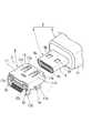
まず、ケーブル側コネクタ2を図1乃至図6を参照して説明する。図1は、本発明の一実施形態を示すケーブル側コネクタ2の外観図であって、図1(A)は、ケーブル側コネクタ2の前面図(正面図)、図1(B)は、ケーブル側コネクタ2の上面図(平面図)、図1(C)は、ケーブル側コネクタ2の下面図(底面図)、図1(D)は、ケーブル側コネクタ2の右側面図である。また、図2は、図1(B)に示すケーブル側コネクタ2のY1−Y1断面図、図3は、図1(B)に示すケーブル側コネクタ2のボディ8を斜め上から見た斜視図、図4は、図1(B)に示すケーブル側コネクタ2をそのフード11及びバックシェルカバー10を除去した状態で斜め上から見た斜視図、図5は、図1(B)に示すケーブル側コネクタ2をそのフード11を除去した状態で斜め上から見た斜視図、図6は、図1(A)に示すケーブル側コネクタ2の嵌合部6の拡大図である。 First, the
図1(A)、図1(B)、図1(C)、図1(D)に示すように、ケーブル側コネクタ2は、ケーブル1との接続部5と、基板実装側コネクタ4との接続部である嵌合部6とを有する。図1(A)、図1(B)、図1(C)における一点鎖線2aは、ケーブル側コネクタ2の接続部5及び嵌合部6の中心線、すなわちケーブル側コネクタ2の中心線を示す。 As shown in FIGS. 1 (A), 1 (B), 1 (C), and 1 (D), the cable-
図2乃至図6に示すように、ケーブル側コネクタ2は、主として、19本(複数本の一例)のコンタクト7と、ボディ8と、シェル(フロントシェル)9と、バックシェルカバー10と、フード11とで構成される。 As shown in FIGS. 2 to 6, the
図2に示すように、コンタクト7は、金属板の打ち抜き加工及び曲げ加工等のプレス加工によって形成された前後方向に延伸する細長い電極端子からなり、導電性を有する。このコンタクト7には、前端部から後側に向かってプリロード用の係止部7a、山状の可動接点部7b、接点付勢用のバネ部7c、固定部7dがこの順に形成され、コンタクト7の後端部に半田付け部7eが形成される。 As shown in FIG. 2, the
図2、図3、図6に示すように、ボディ8は、プラスチック等の絶縁材料からなり、絶縁性を有する。このボディ8には、直方体状のコンタクト支持基部8aと、このコンタクト支持基部8aの前面中央部から前方(基板実装側コネクタ4に対するケーブル側コネクタ2の挿入方向)へ突出する矩形筒状のコンタクト支持部8bとが形成され、このコンタクト支持部8bの前部によって前面を開口した相手コンタクト挿入孔8cが形成される。またコンタクト支持部8bの相対する上下側壁のうち、上側壁の内表面には10本のコンタクト収納溝8dが左右横一列に並べられて前後方向に平行に形成され、下側壁の内表面には9本のコンタクト収納溝8dが左右横一列に並べられて前後方向に平行に形成される。これら上部のコンタクト収納溝8dと下部のコンタクト収納溝8dは、平面視で重ならないよう千鳥状に配列される。 As shown in FIGS. 2, 3, and 6, the
そして、19本のコンタクト7のうち、10本のコンタクト7は、上部のコンタクト収納溝8dに圧入され、コンタクト支持部8bの上側壁に左右横一列に並べられて前後方向に平行に装着される。この装着状態では、固定部7dが上部のコンタクト収納溝8dの後部に圧入固定され、固定部7dより前側のバネ部7c、接点部7b、係止部7aが上部のコンタクト収納溝8dの前部に上下方向に弾性変位可能に挿入収納される。このとき、係止部7aは、バネ部7cの下向きの付勢力によって、バネ部7cの自由復帰位置の少し手前でコンタクト支持部8bの上側壁に上側から係止し、可動接点部7bにプリロード(初期荷重)を掛けた状態で、可動接点部7bをコンタクト収納溝8dの前部から相手コンタクト挿入孔8cの上部に下向きで突出保持する。半田付け部7eは、ボディ8の後側に突出される。 Of the 19
また、残り9本のコンタクト7は、下部のコンタクト収納溝8dに圧入され、コンタクト支持部8bの下側壁に左右横一列に並べられて前後方向に平行に装着される。この装着状態では、固定部7dが下部のコンタクト収納溝8dの後部に圧入固定され、固定部7dより前側のバネ部7c、可動接点部7b、係止部7aが下部のコンタクト収納溝8dの前部に上下方向に弾性変位可能に挿入収納される。このとき、係止部7aは、バネ部7cの上向きの付勢力によって、バネ部7cの自由復帰位置の少し手前でコンタクト支持部8bの下側壁に下側から係止し、可動接点部7bにプリロードを掛けた状態で、可動接点部7bをコンタクト収納溝8dの前部から相手コンタクト挿入孔8cの下部に上向きで突出保持する。半田付け部7eは、ボディ8の後側に突出される。 The remaining nine
こうして、19本のコンタクト7がボディ8に装着保持されて、上下2列に配列され、しかも上部のコンタクト7と下部のコンタクト7が平面視で重ならないよう千鳥状に配列される。 In this way, 19
図2、図4、図5に示すように、シェル9は、一枚の金属板の打ち抜き加工及び曲げ加工等のプレス加工によって形成された前後方向に延伸する金属製の矩形筒からなり、導電性を有する。また、シェル9の矩形筒形状は、図1(A)、図1(B)、図1(C)にも示すように、矩形金属板(展開状態のシェル9)の左右端縁同士をシェル9の下側で、しかもシェル9の中心線2aを中心としてではなく、シェル9の中心線2aから右側(片側の一例)に偏った位置で継ぎ合わせて形成される。したがって、矩形筒状のシェル9は、その下側板が矩形金属板の左右端部によって形成され、その矩形金属板の左右端部同士の継ぎ目9aは、シェル9の下側板に設けられ、しかもシェル9の中心線2aから右側に偏った位置に設けられる。この継ぎ目9aの形状は、一直線ではなく、逆台形状の凹と凸が交互に連なる凹凸形状に形成される。 2, 4, and 5, the
そして、シェル9は、19本のコンタクト7を内側に装着保持したボディ8のコンタクト支持部8bに外嵌され、このコンタクト支持部8bの外表面を覆う。 The
こうして、内側に19本のコンタクト7を装着保持し、かつ外表面を金属製でシールド性を持たせたシェル9で覆われたボディ8のコンタクト支持部8bによって、ケーブル側コネクタ2の嵌合部6が構成される。したがって、この嵌合部6は、その下表面にシェル9の継ぎ目9aが設けられ、しかも嵌合部6の中心線2aから右側に偏った位置に設けられる。 In this way, the fitting portion of the cable-
また、シェル9の上側板には、ケーブル側コネクタ2の基板実装側コネクタ4からの抜去力を高め、多極コネクタの嵌合信頼性を向上させるために、基板実装側コネクタ4に対する係止部としての切欠窓9bが設けられる。この切欠窓9bは、シェル9の中心線2aを対称軸とする左右対称の2箇所に設けられる。したがって、嵌合部6は、その上表面に基板実装側コネクタ4に対する係止部としての切欠窓9bが設けられ、しかも嵌合部6の中心線2aを対称軸とする左右対称の2箇所に設けられる。 In addition, the upper plate of the
こうして、シェル9の継ぎ目9aは、基板実装側コネクタ4に対する係止部としての切欠窓9bが設けられるシェル9の一面(上面)とは、反対側の面(下面)に設けられる。 Thus, the
さらに、シェル9の後側には、下方に開口したコ字形の断面形状を有するバックシェル本体9cと、位置決め板9dとが設けられる。このバックシェル本体9cは、シェル9の上側板の延長部によってシェル9と一体に形成される。位置決め板9dは、シェル9の継ぎ目9aより左側にある横幅の広い下側板の延長部によってシェル9と一体に形成される。 Further, on the rear side of the
バックシェルカバー10は、一枚の金属板の打ち抜き加工及び曲げ加工等のプレス加工によって形成されて導電性を有する。またバックシェル本体9cに被着できるよう上方に開口したコ字形の断面形状を有する。 The
そして、バックシェル本体9cと、このバックシェル本体9cに下側から被着するバックシェルカバー10とで、シェル9と一体であって、シェル9の後側で前後方向に延伸する金属製でシールド性を持たせた矩形筒状のバックシェルを構成する。 The back shell
バックシェル本体9cとバックシェルカバー10は、バックシェル本体9cにバックシェルカバー10を被着した際に左側板同士及び右側板同士が重なり合って電気的に結合されると共に、この重なり合った側板間の凹凸嵌合によって結合一体化される。バックシェルの前部には、ボディ8のコンタクト支持基部8aが内嵌され、バックシェルの前部によってボディ8のコンタクト支持基部8aの外表面が覆われる。また、バックシェルの前部にボディ8のコンタクト支持基部8aが内嵌した際にコンタクト支持基部8aの下表面に位置決め板9dが重なり合い、この重なり合ったコンタクト支持基部8aの下表面と位置決め板9d間の凹凸嵌合によってボディ8とシェル9及びバックシェルの前後方向の位置決めが行われる。 The back shell
また、バックシェルの後側には、バックシェル本体9cの上側板の延長部によって形成されたケーブルシールド接触片9eと、バックシェルカバー10の下側板の延長部によって形成されたケーブルカシメ片10aとが設けられる。 Further, on the rear side of the back shell, a cable
ケーブル側コネクタ2は、ケーブル1との電気接続用にプリント回路基板からなる基板12を備えており、ボディ8の後側に突出された上部のコンタクト7の半田付け部7eが基板12の前端部上表面に半田付けされ、ボディ8の後側に突出された下部のコンタクト7の半田付け部7eが基板12の前端部下表面に半田付けされる。他方、ケーブル1の電源、映像、音声、制御等の各線の芯線の末端が基板12の上表面及び下表面に分けて半田付けされ、ボディ12の後側で19本のコンタクト7とケーブル1の電源、映像、音声、制御等の各線の芯線とが基板12によって電気的に接続される。 The cable-
また、ケーブル1は、外皮(シース)の内側にケーブルシールド1aを備えており、ケーブル1の末端における外皮のむき処理によって露出されたケーブルシールド1aをケーブルシールド接触片9eに接触させ、ケーブルカシメ片10aをケーブルシールド1aの上からケーブルシールド接触片9eを抱き込んだ状態でケーブル1の末端にカシメ固定することによって、ケーブル側コネクタ2のシールド、すなわちシェル9及びバックシェルと、ケーブルシールド1aを電気的に接続すると共に、ケーブル側コネクタ2のバックシェルとケーブル1の末端とを連結する。 Further, the
そして、全コンタクト7の半田付け部7eと、基板12と、ケーブル1の電源、映像、音声、制御等の各線の末端とは、インナーモールドによりプラスチック等の絶縁材料によって一体的に包み込まれて封止され、この封止によってボディ8の後側に直列に配置する直方体状のバックボディ13が形成される。このバックボディ13は、ボディ8のコンタクト支持基部8aと一緒にバックシェルに内嵌され、ボディ8のコンタクト支持基部8aの外表面とバックボディ13の外表面とをバックシェルによって一体的に覆う。さらにはこのバックシェルは、インナーモールドによりプラスチック等の絶縁材料によって包み込まれて封止され、この封止によって長方体状のフード11が形成される。 The
こうして、全コンタクト7の半田付け部7eと基板12とケーブル1の電源、映像、音声、制御等の各線の末端とを包み込んで封止したバックボディ13と、ボディ8のコンタクト支持基部8aと、これらバックボディ13とボディ8のコンタクト支持基部8aとを内嵌し、バックボディ13の外表面とボディ8のコンタクト支持基部8aの外表面を一体的に覆う金属製でシールド性を持ったバックシェルと、このバックシェルを包み込んで封止したフード11とによって、ケーブル側コネクタ2の嵌合部6の後側に、ケーブル側コネクタ2の把持部となるケーブル1との接続部5が構成され、ケーブル側コネクタ2が完成される。フード11は、ケーブル1のカシメ部を越えて皮むき処理されていない外皮の末端部を覆い、この外皮の末端部を覆うフード11の後端部には、ケーブル1の折れ損を防止するためのケーブルブッシュ11aが形成される。 In this way, the
ところで、ケーブル側コネクタ2の19本のコンタクト7は、高速差動信号伝送用の複数組のコンタクト対と、高速差動信号伝送用以外の電気接続用のコンタクトとを含む。便宜上、19本のコンタクトに図6に示すようなコンタクト番号を付けると、1番と3番の隣接する2本のコンタクト7、4番と6番の隣接する2本のコンタクト7、7番と9番の隣接する2本のコンタクト7、10番と12番の隣接する2本のコンタクト7が、それぞれ高速差動信号伝送用のコンタクト対である。このように高速差動信号伝送用の4組のコンタクト対が右側に偏って配列されているので、図6に示すように、シェル9の継ぎ目9aは、シェル9の中心線2aから左側に偏った位置に設けられる。すなわち継ぎ目9aをシェル9の中心線2aから片側に偏らせる際の方向と距離は、継ぎ目9aが高速差動信号伝送用のコンタクト対から遠ざかる方向であって、継ぎ目9aが高速差動信号伝送用のコンタクト対と平面視で重ならない距離に設定される。 By the way, the 19
こうして、シェル9の継ぎ目9aは、高速差動信号伝送用の4組のコンタクト対の配列領域外に設けられる。 Thus, the joint 9a of the
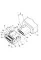
次に、前述したケーブル側コネクタ2の相手コネクタである基板実装側コネクタ4を図7乃至図9を参照して説明する。図7は、本発明の一実施形態を示す基板実装側コネクタ4の外観図であって、図7(A)は、基板実装側コネクタ4の前面図(正面図)、図7(B)は、基板実装側コネクタ4の上面図(平面図)、図7(C)は、基板実装側コネクタ4の下面図(底面図)、図7(D)は、基板実装側コネクタ4の左側面図である。また、図8は、図7(B)に示す基板実装側コネクタ4のY2−Y2断面図、図9は、図7(B)に示す基板実装側コネクタ4のボディ16を斜め上から見た斜視図である。 Next, the
図7(A)、図7(B)、図7(C)、図7(D)に示すように、基板実装側コネクタ4は、ケーブル側コネクタ2との接続部である嵌合部14を有する。図7(A)、図7(B)、図7(C)における一点鎖線4aは、嵌合部14の中心線、すなわち基板実装側コネクタ4の中心線を示す。 As shown in FIG. 7A, FIG. 7B, FIG. 7C, and FIG. 7D, the board mounting
図8、図9にも示すように、基板実装側コネクタ4は、ケーブル側コネクタ2のコンタクト7の接触相手の19本のコンタクト15と、ボディ16と、シェル17とで構成される。 As shown in FIGS. 8 and 9, the board-mounted
コンタクト15は、金属板の打ち抜き加工及び曲げ加工等のプレス加工によって形成されたL形の電極端子からなり、導電性を有する。このコンタクト15には、前後方向に延伸する固定接点部15aと、この固定接点部15aの後端部から下方向へ延伸する固定部15bと、この固定部15bの下端部から後方へ延伸する半田付け部15cが形成される。 The
ボディ16は、プラスチック等の絶縁材料からなり、絶縁性を有する。このボディ16には、直方体状のコンタクト支持基部16aと、このコンタクト支持基部16aの前面中央部から前方(基板実装側コネクタ4に対するケーブル側コネクタ2の挿入方向とは反対方向)へ突出する矩形板状のコンタクト支持部16bとが形成される。 The
そして、19本のコンタクト15のうち、10本のコンタクト15は、固定部15bがコンタクト支持基部16aに固定され、固定接点部15aがコンタクト支持部15aの上表面で左右横一列に並べられて前後方向に平行に固定され、半田付け部15cがコンタクト支持基部16aの後部下側に突出された状態で、ボディ16に装着保持される。 Of the 19
また、残り9本のコンタクト15は、固定部15bがコンタクト支持基部16aに固定され、固定接点部15aがコンタクト支持部15aの下表面で左右横一列に並べられて前後方向に平行に固定され、半田付け部15cがコンタクト支持基部16aの前部下側に突出された状態で、ボディ16に装着保持される。 Further, the remaining nine
こうして、19本のコンタクト15がボディ16に装着保持されて、上下2列に配列され、しかも上部のコンタクト15と下部のコンタクト16が平面視で重ならないよう千鳥状に配列される。 In this way, 19
シェル17は、一枚の金属板の打ち抜き加工及び曲げ加工等のプレス加工によって形成された前後方向に延伸する金属製の矩形筒からなり、導電性を有する。また、シェル17の矩形筒形状は、打ち抜き後の金属板(展開状態のシェル17)の左右端縁同士をシェル17の下側で、しかもシェル17の中心線4aを中心に継ぎ合わせて形成される。したがって、矩形筒状のシェル17は、その下側板が打ち抜き後の金属板の左右端部によって形成され、その打ち抜き後の金属板の左右端部同士の継ぎ目17aは、シェル17の下側板に設けられ、しかもシェル17の中心線4aを中心に設けられる。この継ぎ目17aの形状は、一直線ではなく、逆台形状の凹と凸が交互に連なる凹凸形状に形成される。 The
そして、シェル17には、19本のコンタクト17を装着保持したボディ16が内嵌されており、シェル17の後部によってボディ16のコンタクト支持基部16aの外表面(但し、下面は除く)を覆い、シェル17の前部によってコンタクト支持部16bの周囲をを囲う。また、シェル17は、その後側開口がボディ16のコンタクト支持基部16aに閉鎖され、前面が開口される。 A
こうして、19本のコンタクトの固定接点部15aが配列されたボディ16のコンタクト支持部16bの周囲を囲う金属製でシールド性を持たせたシェル17によって、基板実装側コネクタ4の嵌合部14が構成される。したがって、この嵌合部14は、その下表面にシェル17の継ぎ目17aが設けられ、しかも嵌合部14の中心線4aを中心に設けられる。 Thus, the
また、シェル17の上側板には、ケーブル側コネクタ2の基板実装側コネクタ4からの抜去力を高め、多極コネクタの嵌合信頼性を向上させるために、ケーブル側コネクタ2の切欠窓9bに対する係止部であって、しかもケーブル側コネクタ2のシェル9と基板実装側コネクタ4のシェル17を確実に電気的に接触させ、多極コネクタのシールド性を向上させるための押圧部でもある突起17bが設けられる。この突起17bは、シェル17の上側板を部分的に切り起こしてなる片持ち梁状の板バネ片17cの自由端部によって形成される。この板バネ片17cは、後端が固定端、前端が自由端に設定されて前後方向に延伸し、その前端部を曲げ形成してシェル17の内側上部に下向きに突出する山状の突起17bを形成する。この突起17b及び板バネ片17cは、シェル17の中心線4aを対称軸とする左右対称の2箇所に設けられる。したがって、嵌合部14は、その内側上表面にケーブル側コネクタ2に対する係止部であって押圧部でもある突起17bが設けられ、しかも嵌合部14の中心線4aを対称軸とする左右対称の2箇所に設けられる。 In addition, the upper plate of the
さらに、シェル17には、基板3に対する実装端子としてのアース端子17dが設けられる。このアース端子17dは、シェル17の左右側部の前後中間部と後端部の合計4箇所から下方向に突出される。また、左側の前後2本のアース端子17dはシェル17の左側板の延長部によって形成され、右側の前後2本のアース端子17dはシェル17の右側板の延長部によって形成される。 Further, the
このように構成された基板実装側コネクタ4は、図10乃至図14に示すように、基板3のエッジ部に実装される。この実装時には、4本のアース端子17dが基板3に設けられた4個のアース用スルーホール3aに挿入されて半田付けされる。また、全コンタクト15の半田付け部が前後2列で千鳥状に配列された基板3の図示しないランド部に半田付けされる。 The
次に、前述したケーブル側コネクタ2及び基板実装側コネクタ4とで構成される多極コネクタの作用を図10乃至図14を参照して説明する。図10はケーブル側コネクタ2を基板実装側コネクタ4に嵌合した状態の多極コネクタの断面図、図11は、ケーブル側コネクタ2を基板実装側コネクタ4に嵌合する前の状態の多極コネクタを斜め上から見た斜視図、図12はケーブル側コネクタ2を基板実装側コネクタ4に嵌合した状態の多極コネクタを斜め上から見た斜視図、図13はケーブル側コネクタ2を基板実装側コネクタ4に嵌合する前の状態の多極コネクタを上下逆にして斜め上から見た斜視図、図14はケーブル側コネクタ2を基板実装側コネクタ4に嵌合した状態の多極コネクタを上下逆にして斜め上から見た斜視図である。 Next, the operation of the multipolar connector constituted by the
図11及び図13に示すように、ケーブル側コネクタ2を基板実装側コネクタ4に嵌合する際は、ケーブル側コネクタ2の接続部5を持ち、ケーブル側コネクタ2の嵌合部6を基板実装側コネクタ4の嵌合部14に突き合わせた状態で、ケーブル側コネクタ2の嵌合部6を基板実装側コネクタ4の嵌合部14に挿入嵌合する。この挿入嵌合に伴い、ケーブル側コネクタ2の相手コンタクト挿入孔8cに、基板実装側コネクタ4のコンタクト支持部15aとその上下表面に配列されたコンタクト15の固定接点部15aとが挿入され、コンタクト支持部15aの上表面に配列された上部のコンタクト15の固定接点部15aに、ケーブル側コネクタ2の相手コンタクト挿入孔8cの上部に突出保持された上部のコンタクト7の可動接点部7bが押し付いて接触し、またコンタクト支持部15aの下表面に配列された下部のコンタクト15の固定接点部15aに、ケーブル側コネクタ2の相手コンタクト挿入孔8cの下部に突出保持された下部のコンタクト7の可動接点部7bが押し付いて接触する。これにより、図10、図12及び図14に示すように、ケーブル1がケーブル側コネクタ2と基板実装側コネクタ4を介して基板3に物理的及び電気的に接続される。 As shown in FIGS. 11 and 13, when the
また、ケーブル側コネクタ2の嵌合部6の基板実装側コネクタ4の嵌合部14への挿入嵌合に伴い、基板実装側コネクタ4の嵌合部14の内側上表面に設けられた左右の突起17bが、板バネ片17cを上方へ撓めた状態で、ケーブル側コネクタ2の嵌合部6の上表面に乗り上げ、ケーブル側コネクタ2の嵌合部6の基板実装側コネクタ4の嵌合部14への完全嵌合に伴い、ケーブル側コネクタ2の嵌合部6の上表面に設けられた左右の切欠窓9bが左右の突起17bに一致し、この左右の突起17bが板バネ片17cの付勢力によって左右の切欠窓9bに嵌合保持されるので、ケーブル側コネクタ2の基板実装側コネクタ4からの抜去力が高まり、多極コネクタの嵌合信頼性が向上される。 In addition, the left and right sides provided on the inner upper surface of the
さらに、左右の突起17bは、左右の切欠窓9bに嵌合した際にケーブル側コネクタ2のコンタクト支持部8bの上表面に当接し、板バネ片17cの付勢力によってケーブル側コネクタ2を下側へ押圧するので、ケーブル側コネクタ2のシェル9の下表面が基板実装側コネクタ4のシェル17の内側下表面に押し付いて接触し、ケーブル側コネクタ2と基板実装側コネクタ4のシェル9,17同士が確実に電気的に接触される。また、ケーブル側コネクタ2のシールド(シェル9及びバックシェル)とケーブルシールド1aは、確実に電気的に接触されている。この結果、ケーブルシールド1a、ケーブル側コネクタ2のシールド(シェル9及びバックシェル)、基板実装側コネクタ4のシールド(シェル17)、そして基板3のシールド(アース)が緊密に結合されて、EMI特性のよいシールドを備えることができる。 Further, the left and
ここで、ケーブル側コネクタ2の左右の切欠窓9bを嵌合部6の中心線2aを対称軸とする左右対称の2箇所に設けたので、ケーブル側コネクタ2に抜去力が作用した際にケーブル側コネクタ2が傾いて、コジリを発生させるのを防止することができる。これに対し、ケーブル側コネクタ2の左右の切欠窓9bを嵌合部6の中心線2aに対して非対称の2箇所に設けた場合、ケーブル側コネクタ2に抜去力が作用した際にケーブル側コネクタ2が傾いて、コジリを発生させてしまう。 Here, since the left and
また、基板実装側コネクタ4において、左右の突起17b及び板バネ片17cをシェル17の基板3と反対側、すなわちシェル17の上側板に形成したので、左右の突起17b及び板バネ片17cを形成するための切欠溝から漏れる高周波ノイズ対策は、機器の筐体やEMI抑制シート等を用いて容易に行うことができる。これに対し、左右の突起17b及び板バネ片17cをシェル17の基板3側に形成した場合、左右の突起17b及び板バネ片17cを形成するための切欠溝から漏れる高周波ノイズ対策には、機器の筐体やEMI抑制シート等を用いることができず、その対策が極めて困難になる。 Further, since the left and
また、ケーブル側コネクタ2において、シェル9の継ぎ目9aを切欠窓9bを設けるシェル9の一面(下側板)と反対側の面(上側板)に設けたので、多極コネクタの小型化に対応しやすくなると共に、ケーブル側コネクタ2に抜去力が作用した際にその抜去力によってシェル9の継ぎ目9aが開くのを防止することができる。これに対し、シェル9の継ぎ目9aと切欠窓9bをシェル9の同一面に設けた場合、多極コネクタの小型化に対応することが困難になると共に、ケーブル側コネクタ2に抜去力が作用した際にその抜去力によってシェル9の継ぎ目9aが開いてしまう。 Further, in the
また、基板実装側コネクタ4において、シェル17の継ぎ目17aをシェル17の中心線4aを中心に設けたので、シェル17は、ケーブル側コネクタ2による左右それぞれのコジリ強度を均衡に保つことができ、基板実装側コネクタ4の耐コジリ性を低下させることがなく、向上することができる。これに対し、シェル17の継ぎ目17aをシェル17の中心線4aから偏奇して設けた場合、シェル17は、ケーブル側コネクタ2による左右それぞれのコジリ強度に優劣が生じるので、基板実装側コネクタ4の耐コジリ性を大きく低下させてしまう。 Further, since the joint 17a of the
このようなことから、ケーブル側コネクタ2の切欠窓9bと基板実装側コネクタ4の突起17b及び板バネ片17cをそれぞれのシェル9,17の上側板(基板3と反対側)に設けること、この切欠窓9bと突起17b及び板バネ片17cをそれぞれのシェル9,17の中心線2a,4aを対称軸とする左右対称の2箇所に設けること、ケーブル側コネクタ2及び基板実装側コネクタ4のそれぞれのシェル9,17の継ぎ目9a,17aをシェル9,17の下側板(基板3側)に設けること、基板実装側コネクタ4のシェル17の継ぎ目17aをシェル17の中心線4aを中心に設けることは、有効である。 For this reason, the
そして、ケーブル側コネクタ2のシェル9の継ぎ目9aをシェル9の中心線2aを中心に設けた場合、ケーブル側コネクタ2を基板実装側コネクタ4に嵌合した際にケーブル側コネクタ2のシェル9の継ぎ目9aと基板実装側コネクタ4のシェル17の継ぎ目17が一致し、その一致した継ぎ目9a,17aの隙間より高周波ノイズが漏れるおそれがありEMI対策上問題であるが、図13に示すように、ケーブル側コネクタ2のシェル9の継ぎ目9aは、シェル9の中心線2aから右側に偏った位置に設けたので、図14に示すように、ケーブル側コネクタ2を基板実装側コネクタ4に嵌合した際にケーブル側コネクタ2のシェル9の継ぎ目9aと基板実装側コネクタ4のシェル17の継ぎ目17がずれるので、高周波ノイズが漏れにくくなり、多極コネクタのEMI特性を改善することができる。 When the
また、図6に示すように、ケーブル側コネクタ2において、シェル9の継ぎ目9aは、高速差動信号伝送用の4組のコンタクト対の配列領域外に設けたので、シェル9の継ぎ目9aと高速差動信号伝送ライン(ケーブル側コネクタ2と基板実装側コネクタ4のそれぞれのコンタクト対)がずれるので、高周波ノイズがさらに漏れにくくなり、多極コネクタのEMI特性をさらに改善することができる。なお、シェル9の継ぎ目9aは、その形状が一直線ではなく凹凸形状で幅を持ち、多極コネクタの小型化に伴って、高速差動信号伝送ラインに一部が重なる場合もあるが、凹凸形状の幅の大半が高速差動信号伝送ラインとの重なりをなくすことで、高周波ノイズの漏れを少なくする効果を得ることができる。 Also, as shown in FIG. 6, in the
以上、本実施形態は、電気・電子機器の間を接続する高速インターフェース用のケーブルと電気・電子機器を接続するための多極コネクタで本発明を説明したが、本発明はそれに限定されることなく、その要旨を逸脱しない範囲内で種々変形実施することができる。 As described above, the present embodiment has described the present invention with the high-speed interface cable for connecting between the electric and electronic devices and the multipolar connector for connecting the electric and electronic devices, but the present invention is not limited thereto. However, various modifications can be made without departing from the scope of the invention.
1 ケーブル
1a ケーブルシールド
2 ケーブル側コネクタ(多極プラグ)
2a ケーブル側コネクタの中心線
4 基板実装側コネクタ(相手コネクタ)(多極レセプタクル)
6,14 嵌合部
7,15 コンタクト(7:プラグ側コンタクト 8:レセプタクル側コンタクト)
8,16 ボディ(8:プラグ側ボディ 16:レセプタクル側ボディ)
9,17 シェル(9:プラグ側シェル 17:レセプタクル側シェル)
9a,17a 継ぎ目
9b 切欠窓(係止部)
9c バックシェル本体(バックシェル)
9d バックシェルカバー(バックシェル)1
2a Center line of
6, 14
8, 16 body(8: Plug side body 16: Receptacle side body)
9,17 shell(9: plug side shell 17: receptacle side shell)
9a,
9c Back shell body (back shell)
9d Back shell cover (back shell)
Claims (2)
Translated fromJapanese前記相手コネクタへの嵌合部の周囲の覆いとしての筒状のプラグ側シェルを備え、このプラグ側シェルが金属板の曲げ加工によって形成されてシールド性を持つと共に前記金属板の両端面が突き合わされた継ぎ目を有し、絶縁材料からなるプラグ側ボディに装着された複数本のプラグ側コンタクトが、前記プラグ側シェルの内側に設けられ、高速差動信号用の複数組のプラグ側コンタクト対を含んだ多極プラグにおいて、
前記プラグ側シェルの一面にだけ前記相手コネクタとの係止部を形成し、前記プラグ側シェルの前記継ぎ目は、前記係止部を形成した前記プラグ側シェルの一面とは反対側で前記係止部を形成しない面において、前記多極プラグと前記相手コネクタとを嵌合した際に前記プラグ側シェルの前記継ぎ目と前記レセプタクル側シェルの前記継ぎ目とがずれるための前記プラグ側シェルの中心線から片側に偏った位置で、前記複数組のプラグ側コンタクト対と平面視で重ならない位置に設けたことを特徴とする多極プラグ。The mating connectorincludes a cylindrical receptacle-side shell as a cover around the fitting portion with the multipolar plug, and the receptacle-side shell is formed by bending a metal plate to have a shielding property and the metal plate. A plurality of sets of receptacles for high-speed differential signals, wherein a plurality of receptacle-side contacts attached to a receptacle-side body made of an insulating material have joints with both end faces but are provided inside the receptacle-side shell. A multi-pole receptacle including a pair of side contacts,
Wherein comprising a cylindricalplug shell as covering the periphery of the fitting portion of the mating connector, end surfaces of the metal plate is butted together with theplug shell has a shielding property is formed by bending a metal platehave a combinedseams, a plurality of plug contacts mounted on the plug on the body of insulating material is provided on the inside of the plug shell, a plurality of sets of the plug-side contact pairs for high-speed differential signals In the included multipolar plug,
Whereinonly one side of theplug shell to form the engaging portion with the mating connector, the seamof the plug shell, said locking opposite the one surface of theplug shell forming the locking portion When themultipolar plug and the mating connector are fitted to each other, the plug-side shell seam and the receptacle-side shell seam are displaced from the center line of theplug-side shell. A multipolar plugprovided at a position biased to one side so asnot to overlap the plurality of sets of plug-side contact pairs in plan view .
Priority Applications (6)
| Application Number | Priority Date | Filing Date | Title |
|---|---|---|---|
| JP2009281946AJP5568291B2 (en) | 2009-12-11 | 2009-12-11 | Multi-pole plug |
| TW099131466ATWI489708B (en) | 2009-12-11 | 2010-09-16 | Multi-pole plug |
| KR1020100101986AKR101711656B1 (en) | 2009-12-11 | 2010-10-19 | Multipole plug |
| EP10194032.8AEP2333910B1 (en) | 2009-12-11 | 2010-12-07 | Multipolar plug |
| US12/963,903US8303343B2 (en) | 2009-12-11 | 2010-12-09 | Multipolar plug |
| CN201010588850.XACN102148447B (en) | 2009-12-11 | 2010-12-10 | Multipole plug |
Applications Claiming Priority (1)
| Application Number | Priority Date | Filing Date | Title |
|---|---|---|---|
| JP2009281946AJP5568291B2 (en) | 2009-12-11 | 2009-12-11 | Multi-pole plug |
Publications (2)
| Publication Number | Publication Date |
|---|---|
| JP2011124147A JP2011124147A (en) | 2011-06-23 |
| JP5568291B2true JP5568291B2 (en) | 2014-08-06 |
Family
ID=43567637
Family Applications (1)
| Application Number | Title | Priority Date | Filing Date |
|---|---|---|---|
| JP2009281946AActiveJP5568291B2 (en) | 2009-12-11 | 2009-12-11 | Multi-pole plug |
Country Status (6)
| Country | Link |
|---|---|
| US (1) | US8303343B2 (en) |
| EP (1) | EP2333910B1 (en) |
| JP (1) | JP5568291B2 (en) |
| KR (1) | KR101711656B1 (en) |
| CN (1) | CN102148447B (en) |
| TW (1) | TWI489708B (en) |
Families Citing this family (28)
| Publication number | Priority date | Publication date | Assignee | Title |
|---|---|---|---|---|
| US8366486B1 (en)* | 2011-11-10 | 2013-02-05 | Cheng Uei Precision Industry Co., Ltd. | Electrical connector |
| US8517748B1 (en)* | 2012-07-23 | 2013-08-27 | Vanguard Products Group, Inc. | Communication connector with analog coupling circuit |
| TWM447005U (en)* | 2012-08-14 | 2013-02-11 | Hon Hai Prec Ind Co Ltd | Electronic connector and electronic device using same |
| US20140273594A1 (en)* | 2013-03-14 | 2014-09-18 | Delphi Technologies, Inc. | Shielded cable assembly |
| US11336058B2 (en) | 2013-03-14 | 2022-05-17 | Aptiv Technologies Limited | Shielded cable assembly |
| US10109958B2 (en) | 2013-12-10 | 2018-10-23 | Delphi Technologies, Inc. | Electrical connection system for shielded wire cable |
| JP2015130326A (en)* | 2013-12-10 | 2015-07-16 | デルファイ・テクノロジーズ・インコーポレーテッド | Shielded cable assembly |
| US10211546B2 (en) | 2013-12-10 | 2019-02-19 | Aptiv Technologies Limited | Electrical connection system for shielded wire cable |
| CN106415944A (en) | 2014-04-23 | 2017-02-15 | 泰科电子公司 | Electrical connector with shield cap and shielded terminals |
| JP6422675B2 (en)* | 2014-06-03 | 2018-11-14 | 日本航空電子工業株式会社 | connector |
| JP6055442B2 (en)* | 2014-08-07 | 2016-12-27 | 日本アイエフ株式会社 | Cable connector |
| EP2991169B1 (en)* | 2014-08-27 | 2018-01-31 | TE Connectivity Nederland B.V. | Connector system |
| JP2016072067A (en)* | 2014-09-30 | 2016-05-09 | ホシデン株式会社 | connector |
| JP6404156B2 (en)* | 2015-03-25 | 2018-10-10 | 日本航空電子工業株式会社 | connector |
| JP6452529B2 (en)* | 2015-04-10 | 2019-01-16 | 日本航空電子工業株式会社 | connector |
| TWM517439U (en)* | 2015-10-16 | 2016-02-11 | 唐虞企業股份有限公司 | Single element wire board connection terminal |
| JP6703861B2 (en)* | 2016-02-26 | 2020-06-03 | ヒロセ電機株式会社 | connector |
| CN107978901A (en)* | 2016-10-21 | 2018-05-01 | 富士康(昆山)电脑接插件有限公司 | Micro coaxial cable connector assembly |
| JP6840579B2 (en)* | 2017-03-13 | 2021-03-10 | 日本航空電子工業株式会社 | connector |
| US20200083651A1 (en)* | 2017-03-17 | 2020-03-12 | Invue Security Products Inc. | Security connector |
| US20180366852A1 (en)* | 2017-06-14 | 2018-12-20 | Cvilux Corporation | Connecting cable assembly, electrical connector assembly and paddle card thereof |
| JP7074473B2 (en)* | 2017-12-26 | 2022-05-24 | 株式会社ワコム | Electronic pen |
| TWM565419U (en)* | 2018-02-26 | 2018-08-11 | 宣德科技股份有限公司 | An improved connector assembly |
| US10826243B2 (en)* | 2018-08-28 | 2020-11-03 | Sure-Fire Electrical Corporation | Electric connector terminal configuration structure |
| WO2021010261A1 (en)* | 2019-07-16 | 2021-01-21 | タイコエレクトロニクスジャパン合同会社 | Connector |
| EP3787132B1 (en)* | 2019-08-27 | 2024-06-26 | TE Connectivity Germany GmbH | Connector shielding with a circumferential retention element and method for manufacturing thereof |
| JP7552523B2 (en)* | 2021-07-27 | 2024-09-18 | 株式会社オートネットワーク技術研究所 | Connector System |
| JP2023098099A (en) | 2021-12-28 | 2023-07-10 | ホシデン株式会社 | Connector and connection structure between circuit board and connector |
Family Cites Families (12)
| Publication number | Priority date | Publication date | Assignee | Title |
|---|---|---|---|---|
| JP3425688B2 (en)* | 1999-10-28 | 2003-07-14 | 日本航空電子工業株式会社 | Connector shell structure |
| US6315608B1 (en)* | 2000-03-31 | 2001-11-13 | Molex Incorporated | Channel isolation shield |
| TWM258443U (en)* | 2004-05-13 | 2005-03-01 | Advanced Connectek Inc | Improved connector with a transmission interface |
| JP2007103249A (en)* | 2005-10-06 | 2007-04-19 | Japan Aviation Electronics Industry Ltd | Electrical connector |
| US7371118B2 (en)* | 2006-08-25 | 2008-05-13 | Hon Hai Precision Ind. Co., Ltd | Electrical connector assembly with reduced crosstalk and electromaganetic interference |
| CN201112707Y (en)* | 2007-08-10 | 2008-09-10 | 富士康(昆山)电脑接插件有限公司 | electrical connector |
| US7422488B1 (en)* | 2007-11-02 | 2008-09-09 | Hon Hai Precision Ind. Co., Ltd. | Extension to electrical connector with improved contact arrangement and method of assembling the same |
| TWM330607U (en)* | 2007-11-16 | 2008-04-11 | Wonten Technology Co Ltd | Electric connector |
| JP4544301B2 (en)* | 2007-12-26 | 2010-09-15 | ソニー株式会社 | Image display device and connector display method |
| WO2009115922A2 (en)* | 2008-02-26 | 2009-09-24 | Molex Incorporated | Impedance controlled electrical connector |
| JP3144002U (en)* | 2008-05-19 | 2008-08-14 | 展勝電業股▲ふん▼有限公司 | High frequency digital AV connector |
| US7614920B1 (en)* | 2008-11-17 | 2009-11-10 | Hon Hai Precision Ind. Co., Ltd. | Electrical connector with improved mating port for high speed signal transmission |
- 2009
- 2009-12-11JPJP2009281946Apatent/JP5568291B2/enactiveActive
- 2010
- 2010-09-16TWTW099131466Apatent/TWI489708B/ennot_activeIP Right Cessation
- 2010-10-19KRKR1020100101986Apatent/KR101711656B1/enactiveActive
- 2010-12-07EPEP10194032.8Apatent/EP2333910B1/ennot_activeNot-in-force
- 2010-12-09USUS12/963,903patent/US8303343B2/ennot_activeExpired - Fee Related
- 2010-12-10CNCN201010588850.XApatent/CN102148447B/enactiveActive
Also Published As
| Publication number | Publication date |
|---|---|
| TW201136058A (en) | 2011-10-16 |
| KR20110066843A (en) | 2011-06-17 |
| TWI489708B (en) | 2015-06-21 |
| EP2333910A1 (en) | 2011-06-15 |
| CN102148447B (en) | 2015-02-11 |
| KR101711656B1 (en) | 2017-03-02 |
| EP2333910B1 (en) | 2018-10-17 |
| US20110143594A1 (en) | 2011-06-16 |
| CN102148447A (en) | 2011-08-10 |
| US8303343B2 (en) | 2012-11-06 |
| JP2011124147A (en) | 2011-06-23 |
Similar Documents
| Publication | Publication Date | Title |
|---|---|---|
| JP5568291B2 (en) | Multi-pole plug | |
| US10096947B2 (en) | Electrical connector and electrical device assembled with the same therein | |
| US9559469B2 (en) | Connector | |
| JP6281539B2 (en) | Electric connector device for board connection | |
| TWI578629B (en) | Plug connector and receptacle connector mated with each other | |
| CN104505642B (en) | Plug electric connector | |
| JP5771094B2 (en) | Shield connector | |
| JP6256426B2 (en) | Electrical connector for board connection | |
| CN110350367B (en) | Connector including L-shaped coaxial terminal and method of manufacturing the same | |
| JP2021009836A (en) | Multi-channel connector and assembly thereof | |
| JP6293594B2 (en) | connector | |
| US10741974B2 (en) | Electrical connector | |
| TWI398993B (en) | Electrical connector assembly | |
| CN109378608B (en) | Socket connector | |
| CN201498641U (en) | Electrical connector and electrical connector component | |
| JP4365422B2 (en) | Connector and portable terminal equipped with connector | |
| CN105826709A (en) | Coaxial-type electric connector | |
| TWI543477B (en) | Coaxial electrical connector | |
| JP3116728U (en) | Shielded electrical connector | |
| TW201931687A (en) | Electrical connector assembly | |
| JP6344576B2 (en) | USB connector | |
| TWI472101B (en) | Electrical connector | |
| JP2006286216A (en) | Shield connector | |
| TWM493176U (en) | Electrical connector | |
| TW201803230A (en) | Structure of electrical connector and assembling method thereof capable of effectively restraining noise interference problem, and simply and quickly completing the assembling operation for the transmission conductor set and the cable component |
Legal Events
| Date | Code | Title | Description |
|---|---|---|---|
| A621 | Written request for application examination | Free format text:JAPANESE INTERMEDIATE CODE: A621 Effective date:20120808 | |
| A977 | Report on retrieval | Free format text:JAPANESE INTERMEDIATE CODE: A971007 Effective date:20130723 | |
| A131 | Notification of reasons for refusal | Free format text:JAPANESE INTERMEDIATE CODE: A131 Effective date:20130730 | |
| A521 | Written amendment | Free format text:JAPANESE INTERMEDIATE CODE: A523 Effective date:20130926 | |
| A131 | Notification of reasons for refusal | Free format text:JAPANESE INTERMEDIATE CODE: A131 Effective date:20140304 | |
| A521 | Written amendment | Free format text:JAPANESE INTERMEDIATE CODE: A523 Effective date:20140418 | |
| TRDD | Decision of grant or rejection written | ||
| A01 | Written decision to grant a patent or to grant a registration (utility model) | Free format text:JAPANESE INTERMEDIATE CODE: A01 Effective date:20140527 | |
| A61 | First payment of annual fees (during grant procedure) | Free format text:JAPANESE INTERMEDIATE CODE: A61 Effective date:20140623 | |
| R150 | Certificate of patent or registration of utility model | Ref document number:5568291 Country of ref document:JP Free format text:JAPANESE INTERMEDIATE CODE: R150 |