JP5568212B2 - Substrate processing apparatus, coating method therefor, substrate processing method, and semiconductor device manufacturing method - Google Patents
Substrate processing apparatus, coating method therefor, substrate processing method, and semiconductor device manufacturing methodDownload PDFInfo
- Publication number
- JP5568212B2 JP5568212B2JP2007242630AJP2007242630AJP5568212B2JP 5568212 B2JP5568212 B2JP 5568212B2JP 2007242630 AJP2007242630 AJP 2007242630AJP 2007242630 AJP2007242630 AJP 2007242630AJP 5568212 B2JP5568212 B2JP 5568212B2
- Authority
- JP
- Japan
- Prior art keywords
- gas
- reaction tube
- plasma generation
- processing
- supplying
- Prior art date
- Legal status (The legal status is an assumption and is not a legal conclusion. Google has not performed a legal analysis and makes no representation as to the accuracy of the status listed.)
- Active
Links
Images


Classifications
- C—CHEMISTRY; METALLURGY
- C23—COATING METALLIC MATERIAL; COATING MATERIAL WITH METALLIC MATERIAL; CHEMICAL SURFACE TREATMENT; DIFFUSION TREATMENT OF METALLIC MATERIAL; COATING BY VACUUM EVAPORATION, BY SPUTTERING, BY ION IMPLANTATION OR BY CHEMICAL VAPOUR DEPOSITION, IN GENERAL; INHIBITING CORROSION OF METALLIC MATERIAL OR INCRUSTATION IN GENERAL
- C23C—COATING METALLIC MATERIAL; COATING MATERIAL WITH METALLIC MATERIAL; SURFACE TREATMENT OF METALLIC MATERIAL BY DIFFUSION INTO THE SURFACE, BY CHEMICAL CONVERSION OR SUBSTITUTION; COATING BY VACUUM EVAPORATION, BY SPUTTERING, BY ION IMPLANTATION OR BY CHEMICAL VAPOUR DEPOSITION, IN GENERAL
- C23C16/00—Chemical coating by decomposition of gaseous compounds, without leaving reaction products of surface material in the coating, i.e. chemical vapour deposition [CVD] processes
- C23C16/44—Chemical coating by decomposition of gaseous compounds, without leaving reaction products of surface material in the coating, i.e. chemical vapour deposition [CVD] processes characterised by the method of coating
- C23C16/455—Chemical coating by decomposition of gaseous compounds, without leaving reaction products of surface material in the coating, i.e. chemical vapour deposition [CVD] processes characterised by the method of coating characterised by the method used for introducing gases into reaction chamber or for modifying gas flows in reaction chamber
- C23C16/45523—Pulsed gas flow or change of composition over time
- C23C16/45525—Atomic layer deposition [ALD]
- C23C16/45527—Atomic layer deposition [ALD] characterized by the ALD cycle, e.g. different flows or temperatures during half-reactions, unusual pulsing sequence, use of precursor mixtures or auxiliary reactants or activations
- C23C16/45536—Use of plasma, radiation or electromagnetic fields
- H—ELECTRICITY
- H01—ELECTRIC ELEMENTS
- H01L—SEMICONDUCTOR DEVICES NOT COVERED BY CLASS H10
- H01L21/00—Processes or apparatus adapted for the manufacture or treatment of semiconductor or solid state devices or of parts thereof
- H01L21/67—Apparatus specially adapted for handling semiconductor or electric solid state devices during manufacture or treatment thereof; Apparatus specially adapted for handling wafers during manufacture or treatment of semiconductor or electric solid state devices or components ; Apparatus not specifically provided for elsewhere
- H01L21/67005—Apparatus not specifically provided for elsewhere
- H01L21/67011—Apparatus for manufacture or treatment
- H01L21/67098—Apparatus for thermal treatment
- H01L21/67109—Apparatus for thermal treatment mainly by convection
- C—CHEMISTRY; METALLURGY
- C23—COATING METALLIC MATERIAL; COATING MATERIAL WITH METALLIC MATERIAL; CHEMICAL SURFACE TREATMENT; DIFFUSION TREATMENT OF METALLIC MATERIAL; COATING BY VACUUM EVAPORATION, BY SPUTTERING, BY ION IMPLANTATION OR BY CHEMICAL VAPOUR DEPOSITION, IN GENERAL; INHIBITING CORROSION OF METALLIC MATERIAL OR INCRUSTATION IN GENERAL
- C23C—COATING METALLIC MATERIAL; COATING MATERIAL WITH METALLIC MATERIAL; SURFACE TREATMENT OF METALLIC MATERIAL BY DIFFUSION INTO THE SURFACE, BY CHEMICAL CONVERSION OR SUBSTITUTION; COATING BY VACUUM EVAPORATION, BY SPUTTERING, BY ION IMPLANTATION OR BY CHEMICAL VAPOUR DEPOSITION, IN GENERAL
- C23C16/00—Chemical coating by decomposition of gaseous compounds, without leaving reaction products of surface material in the coating, i.e. chemical vapour deposition [CVD] processes
- C23C16/44—Chemical coating by decomposition of gaseous compounds, without leaving reaction products of surface material in the coating, i.e. chemical vapour deposition [CVD] processes characterised by the method of coating
- C23C16/455—Chemical coating by decomposition of gaseous compounds, without leaving reaction products of surface material in the coating, i.e. chemical vapour deposition [CVD] processes characterised by the method of coating characterised by the method used for introducing gases into reaction chamber or for modifying gas flows in reaction chamber
- C23C16/45523—Pulsed gas flow or change of composition over time
- C23C16/45525—Atomic layer deposition [ALD]
- C23C16/45544—Atomic layer deposition [ALD] characterized by the apparatus
- C23C16/45546—Atomic layer deposition [ALD] characterized by the apparatus specially adapted for a substrate stack in the ALD reactor
- C—CHEMISTRY; METALLURGY
- C23—COATING METALLIC MATERIAL; COATING MATERIAL WITH METALLIC MATERIAL; CHEMICAL SURFACE TREATMENT; DIFFUSION TREATMENT OF METALLIC MATERIAL; COATING BY VACUUM EVAPORATION, BY SPUTTERING, BY ION IMPLANTATION OR BY CHEMICAL VAPOUR DEPOSITION, IN GENERAL; INHIBITING CORROSION OF METALLIC MATERIAL OR INCRUSTATION IN GENERAL
- C23C—COATING METALLIC MATERIAL; COATING MATERIAL WITH METALLIC MATERIAL; SURFACE TREATMENT OF METALLIC MATERIAL BY DIFFUSION INTO THE SURFACE, BY CHEMICAL CONVERSION OR SUBSTITUTION; COATING BY VACUUM EVAPORATION, BY SPUTTERING, BY ION IMPLANTATION OR BY CHEMICAL VAPOUR DEPOSITION, IN GENERAL
- C23C16/00—Chemical coating by decomposition of gaseous compounds, without leaving reaction products of surface material in the coating, i.e. chemical vapour deposition [CVD] processes
- C23C16/44—Chemical coating by decomposition of gaseous compounds, without leaving reaction products of surface material in the coating, i.e. chemical vapour deposition [CVD] processes characterised by the method of coating
- C23C16/455—Chemical coating by decomposition of gaseous compounds, without leaving reaction products of surface material in the coating, i.e. chemical vapour deposition [CVD] processes characterised by the method of coating characterised by the method used for introducing gases into reaction chamber or for modifying gas flows in reaction chamber
- C23C16/45563—Gas nozzles
- C23C16/45574—Nozzles for more than one gas
- C—CHEMISTRY; METALLURGY
- C23—COATING METALLIC MATERIAL; COATING MATERIAL WITH METALLIC MATERIAL; CHEMICAL SURFACE TREATMENT; DIFFUSION TREATMENT OF METALLIC MATERIAL; COATING BY VACUUM EVAPORATION, BY SPUTTERING, BY ION IMPLANTATION OR BY CHEMICAL VAPOUR DEPOSITION, IN GENERAL; INHIBITING CORROSION OF METALLIC MATERIAL OR INCRUSTATION IN GENERAL
- C23C—COATING METALLIC MATERIAL; COATING MATERIAL WITH METALLIC MATERIAL; SURFACE TREATMENT OF METALLIC MATERIAL BY DIFFUSION INTO THE SURFACE, BY CHEMICAL CONVERSION OR SUBSTITUTION; COATING BY VACUUM EVAPORATION, BY SPUTTERING, BY ION IMPLANTATION OR BY CHEMICAL VAPOUR DEPOSITION, IN GENERAL
- C23C16/00—Chemical coating by decomposition of gaseous compounds, without leaving reaction products of surface material in the coating, i.e. chemical vapour deposition [CVD] processes
- C23C16/44—Chemical coating by decomposition of gaseous compounds, without leaving reaction products of surface material in the coating, i.e. chemical vapour deposition [CVD] processes characterised by the method of coating
- C23C16/455—Chemical coating by decomposition of gaseous compounds, without leaving reaction products of surface material in the coating, i.e. chemical vapour deposition [CVD] processes characterised by the method of coating characterised by the method used for introducing gases into reaction chamber or for modifying gas flows in reaction chamber
- C23C16/45563—Gas nozzles
- C23C16/45578—Elongated nozzles, tubes with holes
- C—CHEMISTRY; METALLURGY
- C23—COATING METALLIC MATERIAL; COATING MATERIAL WITH METALLIC MATERIAL; CHEMICAL SURFACE TREATMENT; DIFFUSION TREATMENT OF METALLIC MATERIAL; COATING BY VACUUM EVAPORATION, BY SPUTTERING, BY ION IMPLANTATION OR BY CHEMICAL VAPOUR DEPOSITION, IN GENERAL; INHIBITING CORROSION OF METALLIC MATERIAL OR INCRUSTATION IN GENERAL
- C23C—COATING METALLIC MATERIAL; COATING MATERIAL WITH METALLIC MATERIAL; SURFACE TREATMENT OF METALLIC MATERIAL BY DIFFUSION INTO THE SURFACE, BY CHEMICAL CONVERSION OR SUBSTITUTION; COATING BY VACUUM EVAPORATION, BY SPUTTERING, BY ION IMPLANTATION OR BY CHEMICAL VAPOUR DEPOSITION, IN GENERAL
- C23C16/00—Chemical coating by decomposition of gaseous compounds, without leaving reaction products of surface material in the coating, i.e. chemical vapour deposition [CVD] processes
- C23C16/44—Chemical coating by decomposition of gaseous compounds, without leaving reaction products of surface material in the coating, i.e. chemical vapour deposition [CVD] processes characterised by the method of coating
- C23C16/46—Chemical coating by decomposition of gaseous compounds, without leaving reaction products of surface material in the coating, i.e. chemical vapour deposition [CVD] processes characterised by the method of coating characterised by the method used for heating the substrate
- H—ELECTRICITY
- H01—ELECTRIC ELEMENTS
- H01L—SEMICONDUCTOR DEVICES NOT COVERED BY CLASS H10
- H01L21/00—Processes or apparatus adapted for the manufacture or treatment of semiconductor or solid state devices or of parts thereof
- H01L21/67—Apparatus specially adapted for handling semiconductor or electric solid state devices during manufacture or treatment thereof; Apparatus specially adapted for handling wafers during manufacture or treatment of semiconductor or electric solid state devices or components ; Apparatus not specifically provided for elsewhere
- H01L21/67005—Apparatus not specifically provided for elsewhere
- H01L21/67011—Apparatus for manufacture or treatment
- H01L21/67017—Apparatus for fluid treatment
- H—ELECTRICITY
- H01—ELECTRIC ELEMENTS
- H01L—SEMICONDUCTOR DEVICES NOT COVERED BY CLASS H10
- H01L21/00—Processes or apparatus adapted for the manufacture or treatment of semiconductor or solid state devices or of parts thereof
- H01L21/67—Apparatus specially adapted for handling semiconductor or electric solid state devices during manufacture or treatment thereof; Apparatus specially adapted for handling wafers during manufacture or treatment of semiconductor or electric solid state devices or components ; Apparatus not specifically provided for elsewhere
- H01L21/67005—Apparatus not specifically provided for elsewhere
- H01L21/67242—Apparatus for monitoring, sorting or marking
- H01L21/67253—Process monitoring, e.g. flow or thickness monitoring
Landscapes
- Chemical & Material Sciences (AREA)
- Engineering & Computer Science (AREA)
- Physics & Mathematics (AREA)
- Condensed Matter Physics & Semiconductors (AREA)
- General Physics & Mathematics (AREA)
- Manufacturing & Machinery (AREA)
- Computer Hardware Design (AREA)
- Microelectronics & Electronic Packaging (AREA)
- Power Engineering (AREA)
- Chemical Kinetics & Catalysis (AREA)
- General Chemical & Material Sciences (AREA)
- Materials Engineering (AREA)
- Mechanical Engineering (AREA)
- Metallurgy (AREA)
- Organic Chemistry (AREA)
- Plasma & Fusion (AREA)
- Electromagnetism (AREA)
- Chemical Vapour Deposition (AREA)
Description
Translated fromJapanese本発明は基板処理装置、そのコーティング方法、基板処理方法及び半導体デバイスの製造方法に関し、特に基板が収容される反応管の内部に基板の汚染源が侵入するのを防止又は抑制することができる技術に関する。The present invention is a substrate processingapparatus, the coating method ofitssubstrate processing method and relates to amanufacturing method of a semiconductor device, a technique that can be prevented or suppressed particularly contamination source substrate into the reaction tube in which the substrate is accommodated entering About.
基板が収容される反応管の内部で基板処理を行う基板処理装置では、複数種類の処理ガスを反応管の内部に供給することがあるが、反応管の内部空間を成膜空間とプラズマ生成空間とに区画し、それら処理ガスのうち、一方を成膜空間に直接的に供給し、他方をプラズマ生成空間でプラズマ励起させてから成膜空間に供給する場合がある。この場合、プラズマの生成に伴い、反応管を構成する石英中でイオンが発生し、そのイオン化した汚染物質が反応管を透過して成膜空間に侵入し、基板を汚染するときがある。そのため、反応管の内壁を事前に膜でコーティングし、イオン化した汚染物質の成膜空間への侵入を抑制している(例えば特許文献1参照)。
しかしながら、反応管の内壁を膜でコーティングしたとしても、反応管の内部空間は通常、隔壁により成膜空間とプラズマ生成空間とに区画されているため、主に反応管の成膜空間を構成する部位のみがコーティングされ、反応管のプラズマ生成空間を構成する部位が十分にコーティングされないことがある。この場合、成膜処理におけるプラズマの生成に伴い、汚染物質のイオンが反応管のプラズマ生成空間を構成する部位を透過してプラズマ生成空間に侵入し、そこから成膜空間に侵入して基板を汚染するときがある。 However, even if the inner wall of the reaction tube is coated with a film, the internal space of the reaction tube is usually divided into a film formation space and a plasma generation space by a partition wall, so that it mainly constitutes the film formation space of the reaction tube. Only the part is coated, and the part constituting the plasma generation space of the reaction tube may not be sufficiently coated. In this case, as the plasma is generated in the film formation process, pollutant ions permeate the part of the reaction tube that forms the plasma generation space and enter the plasma generation space. There are times when it is contaminated.
本発明の主な目的は、基板の汚染源が反応管を透過して基板を汚染するのを防止又は抑制することができる基板処理装置、そのコーティング方法、基板処理方法及び半導体デバイスの製造方法を提供することにある。The main purpose of the present invention, a substrate processing apparatus which can be prevented or inhibited from contaminating the substrate contamination source substrate is transmitted through the reactiontube, the coating method ofits, themanufacturing method of a substrate processing method and a semiconductor device It is to provide.
本発明の一態様によれば、
基板が収容される反応管であって、内部空間が、基板に所望の膜が形成される成膜空間とプラズマが生成されるプラズマ生成空間とに隔壁によって区画される前記反応管と、
前記反応管内に所望の処理ガスを供給するガス供給ユニットと、
高周波電力供給ユニットに連結され、前記プラズマ生成空間に配置された少なくとも1対の電極と、
前記反応管内の雰囲気を排気する排気ユニットと、
少なくとも前記ガス供給ユニットを制御する制御部と、
を有し、
前記ガス供給ユニットは、
前記成膜空間に、第1の処理ガスを供給する第1のガス供給ラインと、
前記プラズマ生成空間に、第2の処理ガスを供給する第2のガス供給ラインと、
前記プラズマ生成空間に、前記第1の処理ガスと同じ種類の第3の処理ガスを供給する第3のガス供給ラインと、
を含み、
前記制御部は、
前記反応管に収容される基板に所望の膜を形成するときは、少なくとも前記第1の処理ガスと前記第2の処理ガスとを供給するように前記ガス供給ユニットを制御し、
少なくとも前記反応管の前記プラズマ生成空間を構成する部位を膜でコーティングするときは、少なくとも前記第2の処理ガスと前記第3の処理ガスとを供給して150Å以上の膜厚の膜を形成するように前記ガス供給ユニットを制御することを特徴とする基板処理装置が提供される。According to one aspect of the invention,
A reaction tube in which a substrate is accommodated, wherein the internal space ispartitioned by a partitionwall into a film formation space in which a desired film is formed on the substrate and a plasma generation space in which plasma is generated;
A gas supply unit for supplying a desired processing gas into the reaction tube;
At least one pair of electrodes connected to a high frequency power supply unit and disposed in the plasma generation space;
An exhaust unit for exhausting the atmosphere in the reaction tube;
A control unit for controlling at least the gas supply unit;
Have
The gas supply unit includes:
A first gas supply line for supplying a first processing gas to the film formation space;
A second gas supply line for supplying a second processing gas to the plasma generation space;
A third gas supply line for supplying a third processing gas of the same type as the first processing gas to the plasma generation space;
Including
The controller is
When forming a desired film on the substrate accommodated in the reaction tube, the gas supply unit is controlled to supply at least the first processing gas and the second processing gas,
When coating at least a portion constituting the plasma generation space of the reaction tube with a film, at least the second processing gas and the third processing gas are supplied to form a film having a thickness of 150 mm or more. Thus, a substrate processing apparatus for controlling the gas supply unit is provided.
本発明の他の態様によれば、
内部空間が、基板に所望の膜が形成される成膜空間とプラズマが生成されるプラズマ生成空間とに隔壁によって区画される反応管と、
前記反応管内に第1および第2の処理ガスを供給するガス供給ユニットと、
少なくとも前記ガス供給ユニットを制御する制御部と、前記反応管内の雰囲気を排気する排気ユニットと、
を有し、
前記制御部は、
前記第1の処理ガスを前記プラズマ生成空間に供給し、
前記第1の処理ガスを供給後、前記反応管内の雰囲気を排気し、
前記反応管内の雰囲気を排気後、前記プラズマ生成空間に第2の処理ガスを供給し、
前記第2の処理ガスを供給後、前記反応管内の雰囲気を排気して、
前記反応管の前記プラズマ生成空間を構成する部位に150Å以上の膜厚の膜をコーティングするように、前記ガス供給ユニットおよび前記排気ユニットを制御することを特徴とする基板処理装置が提供される。According to another aspect of the invention,
A reaction tube in which an internal space ispartitioned by a partitionwall into a film formation space where a desired film is formed on a substrate and a plasma generation space where plasma is generated;
A gas supply unit for supplying first and second processing gases into the reaction tube;
A control unit that controls at least the gas supply unit; an exhaust unit that exhausts the atmosphere in the reaction tube;
Have
The controller is
Supplying the first process gas to the plasma generation space;
After supplying the first processing gas, the atmosphere in the reaction tube is exhausted,
After evacuating the atmosphere in the reaction tube, supplying a second processing gas to the plasma generation space,
After supplying the second processing gas, the atmosphere in the reaction tube is exhausted,
There is provided a substrate processing apparatus characterized in that the gas supply unit and the exhaust unit are controlled so as to coat a film having a thickness of 150 mm or more on a portion constituting the plasma generation space of the reaction tube.
本発明の他の態様によれば、
基板が収容される反応管であって、内部空間が、基板に所望の膜が形成される成膜空間
とプラズマが生成されるプラズマ生成空間とに隔壁によって区画される前記反応管と、
前記反応管内に所望の処理ガスを供給するガス供給ユニットと、
高周波電力供給ユニットに連結され、前記プラズマ生成空間に配置された少なくとも1
対の電極と、
前記反応管内の雰囲気を排気する排気ユニットと、
を有する基板処理装置において、少なくとも前記反応管の前記プラズマ生成空間を構成
する部位を所望の膜でコーティングするコーティング方法であって、
前記プラズマ生成空間に第1の処理ガスを供給する工程と、
前記反応管内の雰囲気を排気する工程と、
前記プラズマ生成空間に第2の処理ガスを供給する工程と、
前記反応管内の雰囲気を排気する工程と、
を繰り返して150Å以上の膜厚の膜を形成する工程を有することを特徴とする基板処
理装置のコーティング方法が提供される。According to another aspect of the invention,
A reaction tube in which a substrate is accommodated, wherein the internal space ispartitioned by a partitionwall into a film formation space in which a desired film is formed on the substrate and a plasma generation space in which plasma is generated;
A gas supply unit for supplying a desired processing gas into the reaction tube;
At least one connected to a high frequency power supply unit and disposed in the plasma generation space
A pair of electrodes;
An exhaust unit for exhausting the atmosphere in the reaction tube;
A coating method for coating at least a portion constituting the plasma generation space of the reaction tube with a desired film.
Supplying a first processing gas to the plasma generation space;
Evacuating the atmosphere in the reaction tube;
Supplying a second processing gas to the plasma generation space;
Evacuating the atmosphere in the reaction tube;
There is provided a substrate processing apparatus coating method characterized by having a step of forming a film having a thickness of 150 mm or more by repeating the above.
本発明の一態様に係る基板処理装置によれば、反応管の一定部位を膜でコーティングするときにプラズマ生成空間に第2の処理ガスと第3の処理ガスとを供給するから、少なくとも反応管のプラズマ生成空間を構成する部位が膜でコーティングされる。そのため、実際に基板に膜を形成するときにプラズマ生成空間にプラズマを生成させたとしても、基板の汚染源が反応管のプラズマ生成空間を構成する部位を透過するのを阻止することができる。以上から、基板の汚染源が反応管を透過して基板を汚染するのを防止又は抑制することができる。According to engagementRu board processor to an aspect of the present invention, the supplying the second processing gas and a third process gas into the plasma generating space when coating certain portions of the reaction tube at the membrane, at least The part constituting the plasma generation space of the reaction tube is coated with a film. Therefore, even if a plasma is generated in the plasma generation space when a film is actually formed on the substrate, it is possible to prevent the contamination source of the substrate from passing through the site constituting the plasma generation space of the reaction tube. From the above, it is possible to prevent or suppress the contamination source of the substrate from passing through the reaction tube and contaminating the substrate.
本発明の他の態様に係る基板処理装置のコーティング方法によれば、プラズマ生成空間に第1の処理ガスと第2の処理ガスとを供給するから、少なくとも反応管のプラズマ生成空間を構成する部位が膜でコーティングされる。そのため、実際に基板に膜を形成するときにプラズマ生成空間にプラズマを生成させたとしても、基板の汚染源が反応管のプラズマ生成空間を構成する部位を透過するのを阻止することができる。以上から、基板の汚染源が反応管を透過して基板を汚染するのを防止又は抑制することができる。
本発明のさらに他の態様によれば、
内部空間が、基板に所望の膜が形成される成膜空間とプラズマが生成されるプラズマ生成空間とに隔壁によって区画される反応管における前記プラズマ生成空間に第1の処理ガスを供給する工程と、
前記反応管内の雰囲気を排気する工程と、
前記プラズマ生成空間に第2の処理ガスを供給する工程と、
前記反応管内の雰囲気を排気する工程と、
を繰り返して、
少なくとも前記プラズマ生成空間を構成する部位を150Å以上の膜厚の膜でコーティングする工程と、
前記反応管の前記成膜空間に収容される基板に、前記第1の処理ガスおよび前記第2の処理ガスと同じ種類の第3の処理ガスを供給して所望の膜を形成する工程と、を備えることを特徴とする基板処理方法が提供される。
本発明のさらに他の態様によれば、
内部空間が、基板に所望の膜が形成される成膜空間とプラズマが生成されるプラズマ生成空間とに隔壁によって区画される反応管における前記プラズマ生成空間に第1の処理ガスを供給する工程と、
前記反応管内の雰囲気を排気する工程と、
前記プラズマ生成空間に第2の処理ガスを供給する工程と、
前記反応管内の雰囲気を排気する工程と、
を繰り返して、
少なくとも前記プラズマ生成空間を構成する部位を150Å以上の膜厚の膜でコーティングする工程と、
前記反応管の前記成膜空間に収容される基板に、前記第1の処理ガスおよび前記第2の処理ガスと同じ種類の第3の処理ガスを供給して所望の膜を形成する工程と、を備えることを特徴とする半導体デバイスの製造方法が提供される。According to the coating method of the substrate processing apparatus according to another aspect of the present invention, since the first processing gas and the second processing gas are supplied to the plasma generation space, at least a portion constituting the plasma generation space of the reaction tube Is coated with a membrane. Therefore, even if a plasma is generated in the plasma generation space when a film is actually formed on the substrate, it is possible to prevent the contamination source of the substrate from passing through the site constituting the plasma generation space of the reaction tube. From the above, it is possible to prevent or suppress the contamination source of the substrate from passing through the reaction tube and contaminating the substrate.
According to yet another aspect of the invention,
Supplying a first processing gas to the plasma generation space in a reaction tube in which an internal space ispartitioned by a partitionwall into a film formation space in which a desired film is formed on the substrate and a plasma generation space in which plasma is generated; ,
Evacuating the atmosphere in the reaction tube;
Supplying a second processing gas to the plasma generation space;
Evacuating the atmosphere in the reaction tube;
Repeat
Coating at least a portion constituting the plasma generation space with a film having a thickness of 150 mm or more;
Supplying a third processing gas of the same type as the first processing gas and the second processing gas to a substrate accommodated in the film formation space of the reaction tube to form a desired film; A substrate processing method is provided.
According to yet another aspect of the invention,
Interior space, a step ofsupplying a first processing gas into the plasma generation space in the reaction tube is dividedby the plasma generation space and thepartition wall deposition space and plasma desired film on the substrate is formed is generated ,
Evacuating the atmosphere in the reaction tube;
Supplying a second processing gas to the plasma generation space;
Evacuating the atmosphere in the reaction tube;
Repeat
Coating at least a portion constituting the plasma generation space with a film having a thickness of 150 mm or more;
Supplying a third processing gas of the same type as the first processing gas and the second processing gas to a substrate accommodated in the film formation space of the reaction tube to form a desired film; A method for manufacturing a semiconductor device is provided.
以下、図面を参照しながら本発明の好ましい実施形態を説明する。 Hereinafter, preferred embodiments of the present invention will be described with reference to the drawings.
[第1の実施形態]
本実施形態に係る基板処理装置は、半導体装置集積回路(IC(Integrated Circuits))の製造に使用される半導体製造装置の一例として構成されているものである。下記の説明では、基板処理装置の一例として、基板に対し熱処理等をおこなう縦型の装置を使用した場合について述べる。[First Embodiment]
The substrate processing apparatus according to the present embodiment is configured as an example of a semiconductor manufacturing apparatus used for manufacturing a semiconductor device integrated circuit (IC (Integrated Circuits)). In the following description, a case where a vertical apparatus that performs heat treatment or the like on a substrate is used as an example of the substrate processing apparatus will be described.
図1に示す通り、基板処理装置101では、基板の一例となるウエハ200を収納したカセット110が使用されており、ウエハ200はシリコン等の材料から構成されている。基板処理装置101は筐体111を備えており、筐体111の内部にはカセットステージ114が設置されている。カセット110はカセットステージ114上に工場内搬送装置(図示略)によって搬入されたり、カセットステージ114上から搬出されるようになっている。 As shown in FIG. 1, in the
カセットステージ114は、工場内搬送装置によって、カセット110内のウエハ200が垂直姿勢を保持しかつカセット110のウエハ出し入れ口が上方向を向くように載置される。カセットステージ114は、カセット110を筐体111の後方に右回り縦方向90°回転し、カセット110内のウエハ200が水平姿勢となり、カセット110のウエハ出し入れ口が筐体111の後方を向くように動作可能となるよう構成されている。 The
筐体111内の前後方向の略中央部にはカセット棚105が設置されており、カセット棚105は複数段複数列にて複数個のカセット110を保管するように構成されている。カセット棚105にはウエハ移載機構125の搬送対象となるカセット110が収納される移載棚123が設けられている。 A
カセットステージ114の上方には予備カセット棚107が設けられ、予備的にカセット110を保管するように構成されている。 A
カセットステージ114とカセット棚105との間には、カセット搬送装置118が設置されている。カセット搬送装置118は、カセット110を保持したまま昇降可能なカセットエレベータ118aと、搬送機構としてのカセット搬送機構118bとで構成されている。カセット搬送装置118はカセットエレベータ118aとカセット搬送機構118bとの連続動作により、カセットステージ114とカセット棚105と予備カセット棚107との間で、カセット110を搬送するように構成されている。 A
カセット棚105の後方には、ウエハ移載機構125が設置されている。ウエハ移載機構125は、ウエハ200を水平方向に回転ないし直動可能なウエハ移載装置125aと、ウエハ移載装置125aを昇降させるためのウエハ移載装置エレベータ125bとで構成されている。ウエハ移載装置125aにはウエハ200をピックアップするためのツイーザ125cが設けられている。ウエハ移載装置125はウエハ移載装置125aとウエハ移載装置エレベータ125bとの連続動作により、ツイーザ125cをウエハ200の載置部として、ウエハ200をボート217に対して装填(チャージング)したり、ボート217から脱装(ディスチャージング)するように構成されている。 A
筐体111の後部上方には、ウエハ200を熱処理する処理炉202が設けられており、処理炉202の下端部が炉口シャッタ147により開閉されるように構成されている。 A
処理炉202の下方には処理炉202に対しボート217を昇降させるボートエレベータ115が設けられている。ボートエレベータ115の昇降台にはアーム128が連結されており、アーム128にはシールキャップ219が水平に据え付けられている。シールキャップ219はボート217を垂直に支持するとともに、処理炉202の下端部を閉塞可能なように構成されている。 Below the
ボート217は複数の保持部材を備えており、複数枚(例えば50〜150枚程度)のウエハ200をその中心を揃えて垂直方向に整列させた状態で、それぞれ水平に保持するように構成されている。 The
カセット棚105の上方には、清浄化した雰囲気であるクリーンエアを供給するクリーンユニット134aが設置されている。クリーンユニット134aは供給ファン及び防塵フィルタで構成されており、クリーンエアを筐体111の内部に流通させるように構成されている。 Above the
筐体111の左側端部には、クリーンエアを供給するクリーンユニット134bが設置されている。クリーンユニット134bも供給ファン及び防塵フィルタで構成されており、クリーンエアをウエハ移載装置125aやボート217等の近傍を流通させるように構成されている。当該クリーンエアは、ウエハ移載装置125aやボート217等の近傍を流通した後に、筐体111の外部に排気されるようになっている。 A
次に、基板処理装置101の主な動作について説明する。 Next, main operations of the
工場内搬送装置(図示略)によってカセット110がカセットステージ114上に搬入されると、カセット110は、ウエハ200がカセットステージ114の上で垂直姿勢を保持し、カセット110のウエハ出し入れ口が上方向を向くように載置される。その後、カセット110は、カセットステージ114によって、カセット110内のウエハ200が水平姿勢となり、カセット110のウエハ出し入れ口が筐体111の後方を向くように、筐体111の後方に右周り縦方向90°回転させられる。 When the
その後、カセット110は、カセット棚105ないし予備カセット棚107の指定された棚位置へカセット搬送装置118によって自動的に搬送され受け渡され、一時的に保管された後、カセット棚105ないし予備カセット棚107からカセット搬送装置118によって移載棚123に移載されるか、もしくは直接移載棚123に搬送される。 Thereafter, the
カセット110が移載棚123に移載されると、ウエハ200はカセット110からウエハ移載装置125aのツイーザ125cによってウエハ出し入れ口を通じてピックアップされ、ボート217に装填(チャージング)される。ボート217にウエハ200を受け渡したウエハ移載装置125aはカセット110に戻り、後続のウエハ110をボート217に装填する。 When the
予め指定された枚数のウエハ200がボート217に装填されると、処理炉202の下端部を閉じていた炉口シャッタが開き、処理炉202の下端部が開放される。その後、ウエハ200群を保持したボート217がボートエレベータ115の上昇動作により処理炉202内に搬入(ローディング)され、処理炉202の下部がシールキャップ219により閉塞される。 When a predetermined number of
ローディング後は、処理炉202にてウエハ200に対し任意の熱処理が実施される。その熱処理後は、上述の逆の手順で、ウエハ200およびカセット110が筐体111の外部に搬出される。 After loading, arbitrary heat treatment is performed on the
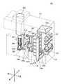
図2に示す通り、処理炉202には加熱装置であるヒータ207が設けられている。ヒータ207は断熱材とヒータ素線とを有し、断熱材をヒータ素線で取り巻いた構成を有している(図示略)。ヒータ207の内側には、基板の一例であるウエハ200が収容される反応管203が設けられている。反応管203は石英で構成されている。反応管203の下端開口はOリング220を介して蓋体であるシールキャップ219により気密に閉塞されている。本実施形態では、少なくとも、反応管203及びシールキャップ219により処理室201が形成されている。 As shown in FIG. 2, the
シールキャップ219にはボート支持台218を介して基板保持部材であるボート217が立設されている。ボート支持台218はボートを保持する保持体となっている。ボート217は処理室201に挿入されている。ボート217にはバッチ処理される複数枚のウエハ200が水平姿勢を保持した状態で図2中上下方向に多段に積載されている。ヒータ207は処理室201に挿入されたウエハ200を所定の温度に加熱する。 A
処理室201の下部には複数種類の処理ガスを供給する3本のガス供給管232a,232b,300が接続されている。 Three
ガス供給管232aには、流量制御装置であるマスフローコントローラ241a及び開閉弁であるバルブ243aが設けられている。ガス供給管232aにはNH3ガス等の処理ガスが流入され、その処理ガスが反応管203内に形成されたバッファ室237(後述参照)を介して処理室201に供給される。The
ガス供給管232bには、流量制御装置であるマスフローコントローラ241b、開閉弁であるバルブ243b、ガス溜め部247及び開閉弁であるバルブ243cが設けられている。ガス供給管232bにはDCSガス等の処理ガスが流入され、その処理ガスがガス供給部249(後述参照)を介して処理室201に供給される。 The
ガス供給管300には、流量制御装置であるマスフローコントローラ302及び開閉弁であるバルブ304が設けられている。ガス供給管300にはDCSガス等の処理ガスが流入され、その処理ガスが反応管203内に形成されたバッファ室237(後述参照)を介して処理室201に供給される。 The
以上のガス供給管232a,232b,300にはガス供給管310,320,330がそれぞれ接続されている。ガス供給管310,320,330には流量制御装置であるマスフローコントローラ312,322,332及び開閉弁であるバルブ314,324,334がそれぞれ設けられている。ガス供給管310,320,330にはN2等の不活性ガスが流入される。
処理室201には処理室201内の雰囲気を排気するガス排気管231の一端部が接続されている。ガス排気管231にはバルブ243dが設けられている。ガス排気管231の他端部は排気装置である真空ポンプ246に接続されており、処理室201内が真空排気されるようになっている。バルブ243dは弁を開閉して処理室201の真空排気・真空排気停止ができ、更に弁開度を調節して圧力調整可能になっている開閉弁である。 One end of a
図3に示す通り、処理室201を構成している反応管203の内壁とウエハ200との間における円弧状の空間には石英製の隔壁236が設けられている。隔壁236は端部が反応管203の内壁に密着した状態で図3中の紙面の裏側から表側に向けて(図2中上下方向)に延在している。図2に示す通り隔壁236の上下端も反応管203の内壁に密着しており、隔壁236の内部には隔壁236と反応管203の一部とで囲まれたバッファ室237が形成されている。すなわち、反応管203の内部空間が隔壁236で区画されている。 As shown in FIG. 3, a
隔壁236のウエハ200に対向配置された部位には複数のガス供給孔248aが設けられている。ガス供給孔248aは反応管203の中心へ向けて開口している。ガス供給孔248aは、図2中下方から上方にわたってそれぞれ同一の開口面積を有し、更に同じ開口ピッチで設けられている。 A plurality of gas supply holes 248 a are provided in a portion of the
バッファ室237のガス供給孔248aが設けられた端部と反対側の端部には、ノズル233が設けられている。ノズル233にはガス供給管232aが接続されており、ガス供給管232aの中途部にはガス供給管300が接続されている。ノズル233は、反応管203の下部より上部にわたり図2中上下方向に沿って延在している。 A
ノズル233には複数のガス供給孔248bが設けられている。ガス供給孔248bは、バッファ室237内と処理室201内との差圧が小さい場合には、ガスの上流側から下流側まで同一の開口面積で同一の開口ピッチで設けられ、逆に差圧が大きい場合には上流側から下流側に向かって開口面積が大きいか、又は開口ピッチが小さくなっている。 The
本実施形態においては、ガス供給孔248bの開口面積は上流側から下流側にかけて徐々に大きくなっている。このように構成することで、ガスが各ガス供給孔248bからバッファ室237に噴出される際には、そのガスは流速に差はあるが流量はほぼ同量となり、その後当該ガスはバッファ室237内において粒子速度差が緩和され、ガス供給孔248aから処理室201に噴出される。よって、ガス供給孔248bから噴出されたガスは、ガス供給孔248aから噴出される際には均一な流量と流速とを有する。 In the present embodiment, the opening area of the
バッファ室237には、細長い構造を有する1対の棒状電極269,270が設けられている。棒状電極269,270は図2中上方から下方に向けて延在しており、棒状電極269,270は電極保護管275に被覆され保護されている。棒状電極269,270のいずれか一方は整合器272を介して高周波電源273に接続され、他方は基準電位であるアースに接続されている。棒状電極269,270に高周波電力が供給されると、その棒状電極269,270間のプラズマ生成領域224にプラズマが生成される。本実施形態では、少なくとも整合器272及び高周波電源273で高周波電力供給ユニットが形成されている。 The
電極保護管275は、棒状電極269,270のそれぞれをバッファ室237の雰囲気と隔離した状態でバッファ室237に挿入できる構造となっている。電極保護管275の内部は外気(大気)と同一雰囲気であると、電極保護管275にそれぞれ挿入された棒状電極269,270はヒータ207の加熱で酸化されてしまう。そこで本実施形態では、棒状電極269,270の酸化を防止するための不活性ガスパージ機構が設けられており(図示略)、電極保護管275の内部は窒素などの不活性ガスで充填あるいはパージされ、酸素濃度が充分低く抑えられている。 The
図3に示す通り、反応管203の内部にはガス供給部249(ノズル)が設けられている。ガス供給部249にはガス供給管232bが接続されている。ガス供給部249は、反応管203の中央部を中心としてガス供給孔248aの位置から約60°程度ずれた位置に設けられている。ガス供給部249は、ALD法による成膜においてウエハ200へ、複数種類のガスを1種類ずつ交互に供給する際に、バッファ室237とガス供給種を分担する供給部である。 As shown in FIG. 3, a gas supply unit 249 (nozzle) is provided inside the
ガス供給部249には、ウエハ200と対向する位置に複数のガス供給孔248cが設けられている。ガス供給孔248cは図2中上下方向に延在している。 The
ガス供給孔248cの開口面積は、ガス供給部249内と処理室201内との差圧が小さい場合には、ガスの上流側から下流側まで同一の開口面積で同一の開口ピッチとすると良いが、差圧が大きい場合には上流側から下流側に向かって開口面積を大きくするか開口ピッチを小さくすると良い。本実施形態においては、ガス供給孔248cの開口面積は上流側から下流側にかけて徐々に大きくなっている。 The opening area of the
図2に示す通り、反応管203内の中央部には複数枚のウエハ200を多段に同一間隔で載置するボート217が設けられている。ボート217はボートエレベータ115(図1参照)により反応管203に出入りできるようになっている。ボート217の下方には、処理の均一性を向上する為にボート217を回転させるための回転装置であるボート回転機構267が設けられている。ボート回転機構267を回転させることにより、ボート支持台218に保持されたボート217を回転させるようになっている。 As shown in FIG. 2, a
制御手段であるコントローラ280は、マスフローコントローラ241a,241b,302,312,322,332、バルブ243a,243b,243c,243d,304,314,324,334、ヒータ207、真空ポンプ246、ボート回転機構267、ボートエレベータ115、高周波電源273、整合器272等に接続されている。 The
本実施形態では、コントローラ280により、マスフローコントローラ241a,241b,302,312,322,332の流量調整、バルブ243a,243b,243c,304,314,324,334の開閉動作、バルブ243dの開閉及び圧力調整動作、ヒータ207の温度調節、真空ポンプ246の起動・停止、ボート回転機構267の回転速度調節、ボートエレベータ115の昇降動作制御、高周波電源273の電力供給制御、整合器272によるインピーダンス制御等が行われる。 In this embodiment, the
次に、ALD法による成膜例について、半導体デバイスの製造工程の一つである、DCSガス及びNH3ガスを用いてSiN膜を成膜する例を説明する。Next, as an example of film formation by the ALD method, an example of forming a SiN film using DCS gas and NH3 gas, which is one of semiconductor device manufacturing processes, will be described.
CVD(Chemical Vapor Deposition)法の中の1つであるALD(Atomic Layer Deposition)法は、ある成膜条件(温度、時間等)の下で、成膜に用いる2種類(またはそれ以上)の原料となる処理ガスを1種類ずつ交互に基板上に供給し、1原子層単位で吸着させ、表面反応を利用して成膜を行う手法である。 ALD (Atomic Layer Deposition), one of the CVD (Chemical Vapor Deposition) methods, uses two (or more) raw materials for film formation under certain film formation conditions (temperature, time, etc.). In this method, one type of processing gas is alternately supplied onto the substrate, adsorbed in units of one atomic layer, and film formation is performed using a surface reaction.
利用する化学反応は、例えばSiN(窒化珪素)膜形成の場合ALD法ではDCS(SiH2Cl2、ジクロルシラン)とNH3(アンモニア)を用いて300〜600℃の低温で高品質の成膜が可能である。また、ガス供給は、複数種類の処理ガスを1種類ずつ交互に供給する。そして、膜厚制御は、処理ガス供給のサイクル数で制御する。(例えば、成膜速度が1Å/サイクルとすると、20Åの膜を形成する場合、処理を20サイクル行う。)For example, in the case of forming a SiN (silicon nitride) film, the ALD method uses DCS (SiH2 Cl2 , dichlorosilane) and NH3 (ammonia) to form a high-quality film at a low temperature of 300 to 600 ° C. Is possible. Further, the gas supply alternately supplies a plurality of types of processing gases one by one. The film thickness is controlled by the number of processing gas supply cycles. (For example, assuming that the film formation rate is 1 mm / cycle, the process is performed 20 cycles when a film of 20 mm is formed.)
後述の成膜処理に先立ち、始めに下記のコーティング処理を行う。なお、下記のコーティング処理ではウエハ200を反応管203に収容しない状態で行う。 Prior to the film forming process described later, first, the following coating process is performed. In the coating process described below, the
[コーティング処理]
NH3ガスをガス供給管232aに流入させた状態でバルブ243a,243dを開ける。NH3ガスをマスフローコントローラ241aで流量調整しながらノズル233のガス供給孔248bからバッファ室237に噴出させ、NH3ガスをガス供給孔248aから処理室201に供給しつつガス排気管231から排気する。このとき、棒状電極269,270には高周波電力を供給せず、NH3ガスをプラズマ励起させない。またヒータ207を制御してバッファ室237の温度を580〜630℃の範囲に設定する。一定時間経過したら、バルブ243aを閉じてNH3ガスの供給を停止するとともに、N2ガスをガス供給管310に流入させた状態でバルブ314を開いてN2ガスで処理室201等のNH3ガスをパージする。[Coating treatment]
The
その後、DCSガスをガス供給管300に流入させた状態でバルブ304を開ける。DCSガスをマスフローコントローラ302で流量調整しながらノズル233のガス供給孔248bからバッファ室237に噴出させ、DCSガスをガス供給孔248aから処理室201に供給しつつガス排気管231から排気する。その結果、主に、反応管203のバッファ室237を構成する部位の内壁と隔壁236の内壁とにSiN膜500が形成される。また、上記の処理では、NH3ガスとDCSガスとがバッファ室237を通過してガス供給孔248aから処理室201にも供給されるから、SiN膜500の形成と併せて、反応管203の成膜空間を構成する部位の内壁と隔壁236の外壁とにSiN膜510も形成される。Thereafter, the
一定時間経過したら、バルブ304を閉じてDCSガスの供給を停止するとともに、N2ガスをガス供給管330に流入させた状態でバルブ334を開いてN2ガスで処理室201等のDCSガスをパージする。After lapse of a fixed time, stops the supply of the DCS gas by closing the
以上の処理を複数回繰り返し、主に、バッファ室237の内部を所定膜厚のSiN膜500でコーティングする。後述の成膜処理で電極269,270に50Wの高周波電力を供給する場合には、コーティングはSiN膜500の膜厚が150Å以上に達するまで続ける。SiN膜500の膜厚を150Å以上とすれば、電極269,270に50Wの高周波電力を供給しても、ウエハ200の汚染源であるNaのバッファ室237への侵入を1×10¹⁰atoms/cm2以下に抑制することができる。汚染源のNaの侵入量は電極269,270への高周波電力量(放電パワー)に比例して増大すると考えられている。The above process is repeated a plurality of times, and the inside of the
なお、上記のコーティング処理では、DCSガスに代えてこれと同種のガス(Siを含むガス)を用いてもよい。 In the above coating process, the same type of gas (a gas containing Si) may be used instead of the DCS gas.
更に、上記のコーティング処理では、バッファ室237の内部のSiN膜500でのコーティングに伴い、結果的にバッファ室237の外部を同時にSiN膜510でコーティングするような構成となっているが、バッファ室237の内部のSiN膜500でのコーティング処理とは別個に、バッファ室237の外部をSiN膜510でコーティングするような構成としてもよい。 Further, in the above-described coating process, the
バッファ室237の外部をコーティングする場合は、下記のような処理を行う。 When coating the outside of the
NH3ガスをガス供給管232aに流入させた状態でバルブ243a,243dを開ける。NH3ガスをマスフローコントローラ241aで流量調整しながらノズル233のガス供給孔248bからバッファ室237に噴出させ、ガス供給孔248aから処理室201に供給しつつガス排気管231から排気する。このとき、棒状電極269,270には高周波電力を供給せず、NH3ガスをプラズマ励起させない。またヒータ207を制御してバッファ室237の温度を580〜630℃の範囲に設定する。一定時間経過したら、バルブ243aを閉じてNH3ガスの供給を停止するとともに、N2ガスをガス供給管310に流入させた状態でバルブ314を開いてN2ガスで処理室201等のNH3ガスをパージする。The
その後、DCSガスをガス供給管232bに流入させた状態でバルブ243b,243cを開ける。DCSガスをマスフローコントローラ241bで流量調整しながらガス供給部249のガス供給孔248cから処理室201に噴出させ、DCSガスを処理室201に供給しつつガス排気管231から排気する。その結果、主に、反応管203の内壁と隔壁236の外壁とにSiN膜510が形成される。一定時間経過したら、バルブ243b,243cを閉じてDCSガスの供給を停止するとともに、N2ガスをガス供給管320に流入させた状態でバルブ324を開いてN2ガスで処理室201等のDCSガスをパージする。Thereafter, the
以上の処理を複数回繰り返し、主に、処理室201の内部であってバッファ室237の外部を所定膜厚のSiN膜510でコーティングする。 The above processing is repeated a plurality of times, and the inside of the
[成膜処理]
次に、ウエハ200への成膜処理を行う。
成膜しようとするウエハ200をボート217に装填し、処理室201に搬入する。搬入後は次の4つのステップの処理を順次実行する。[Film formation]
Next, a film forming process on the
A
(ステップ1)
ステップ1では、プラズマ励起の必要なNH3ガスと、プラズマ励起の必要のないDCSガスとを並行して流す。
始めに、NH3ガスをガス供給管232aに流入させた状態で、ガス供給管232aのバルブ243aとガス排気管231のバルブ243dとを共に開ける。NH3ガスをマスフローコントローラ241aにより流量調整しながらノズル233のガス供給孔248bからバッファ室237へ噴出させる。この状態で、棒状電極269,270に高周波電源273から整合器272を介して高周波電力を供給し、NH3ガスをプラズマ励起させ活性種として処理室201に供給しつつガス排気管231から排気する。(Step 1)
In step 1, NH3 gas that requires plasma excitation and DCS gas that does not require plasma excitation are flowed in parallel.
First, the
NH3ガスをプラズマ励起することにより活性種として流すときは、バルブ243dを適正に調整して処理室201内圧力を10〜100Paの範囲であって、例えば50Paに維持する。マスフローコントローラ241aを制御して、NH3ガスの供給流量を1〜10slmの範囲であって、例えば5slmとする。NH3ガスをプラズマ励起させることにより得られた活性種をウエハ200に晒す時間を2〜120秒間とする。このとき、ヒータ207を制御してウエハ200の温度を300〜600℃(好ましくは450〜550℃)の範囲であって、例えば530℃に設定する。NH3ガスは反応温度が高いため、上記ウエハ温度では反応しない。本実施形態では、NH3ガスをプラズマ励起させ活性種としてから流すようにしており、当該処理はウエハ200の温度を低い温度範囲に設定したままで行える。When flowing the NH3 gas as the active species by plasma excitation is in the range of 10~100Pa a properly adjusted to the
NH3ガスをプラズマ励起させることにより活性種として供給しているとき、ガス供給管232bの上流側のバルブ243bを開け、下流側のバルブ243cを閉めて、DCSガスも流すようにする。これにより、バルブ243b,243c間に設けたガス溜め部247にDCSガスを溜める。このとき、処理室201内に流しているガスはNH3をプラズマ励起させることにより得られた活性種であり、処理室201にはDCSガスは存在しない。したがって、NH3ガスは気相反応を起こすことなく、プラズマにより励起され活性種となったNH3ガスがウエハ200上の下地膜などの表面部分と表面反応(化学吸着)する。When NH3 gas is supplied as active species by plasma excitation, the valve 243b on the upstream side of the
(ステップ2)
ステップ2では、ガス供給管232aのバルブ243aを閉めてNH3ガスの供給を停止し、その一方で引き続きDCSガスを流し続けてガス溜め部247へのDCSガスの供給を継続する。ガス溜め部247に所定圧、所定量のDCSガスが溜まったら、上流側のバルブ243bも閉めて、ガス溜め部247にDCSガスを閉じ込めておく。また、ガス排気管231のバルブ243dは開いたままにし、真空ポンプ246により処理室201の雰囲気を20Pa以下に排気し、処理室201に残留したNH3ガスを処理室201から排除する。(Step 2)
In step 2, the supply of NH3 gas is stopped by closing the
また、このときには、N2ガスをガス供給管310に流入させた状態でバルブ314を開き、N2ガスを処理室201に供給してもよく、この場合には処理室201に残留したNH3ガスを排除する効果が更に高まる。ガス溜め部247内には、圧力が20000Pa以上になるようにDCSガスを溜める。ガス溜め部247と処理室201との間のコンダクタンスが1.5×10⁻³m3/s以上になるように装置を構成する。Further, at this time, the N2 gas by opening the valve 314 in a state of being flowed into the
例えば、反応管203の容積とこれに対する必要なガス溜め部247の容積との比として考えると、反応管203の容積が100l(リットル)である場合においては、ガス溜め部247の容積は100〜300ccであることが好ましく、容積比としてはガス溜め部247の容積を反応管203の容積の1/1000〜3/1000倍とすることが好ましい。 For example, when considering the ratio of the volume of the
(ステップ3)
ステップ3では、処理室201の排気が終わったら、ガス排気管231のバルブ243dを閉じて排気を止める。ガス供給管232bの下流側のバルブ243cを開く。これにより、ガス溜め部247に溜められたDCSガスが、ガス供給部249のガス供給孔248cを通じて処理室201に一気に供給される。このとき、ガス排気管231のバルブ243dが閉じられているので、処理室201内の圧力は急激に上昇して約931Pa(7Torr)まで昇圧される。DCSガスを供給するための時間を2〜4秒と設定し、その後上昇した圧力雰囲気中に晒す時間を2〜4秒に設定し、合計6秒とする。このとき、ヒータ207を制御してウエハ200の温度をNH3ガスの供給時と同じく、300〜600℃(好ましくは450〜550℃)の範囲内であって例えば530℃に維持する。DCSガスの供給により、ウエハ200の表面に化学吸着したNH3とDCSとが反応(化学吸着)して、ウエハ200上にSiN膜が形成される。(Step 3)
In step 3, when the exhaust of the
(ステップ4)
成膜後のステップ4では、バルブ243cを閉じ、バルブ243dを開けて処理室201を真空排気し、処理室201に残留したDCSガスであって成膜に寄与した後のDCSガスを排除する。また、このときには、N2ガスをガス供給管320に流入させた状態でバルブ324を開き、N2ガスを処理室201に供給してもよく、この場合には処理室201に残留したDCSガスであって成膜に寄与した後のDCSガスを処理室201から排除する効果が更に高まる。そして、バルブ243bを開いて、ガス溜め部247へのDCSガスの供給を開始する。(Step 4)
In step 4 after the film formation, the
上記ステップ1〜4を1サイクルとし、このサイクルを複数回繰り返すことによりウエハ200上に所定膜厚のSiN膜を形成する。 Steps 1 to 4 are defined as one cycle, and a SiN film having a predetermined thickness is formed on the
ALD装置では、ガスはウエハ200の表面部分に化学吸着する。このガスの吸着量は、ガスの圧力、及びガスの暴露時間に比例する。よって、希望する一定量のガスを、短時間で吸着させるためには、ガスの圧力を短時間で大きくする必要がある。この点で、本実施形態では、バルブ243dを閉めたうえで、ガス溜め部247内に溜めたDCSガスを瞬間的に供給しているので、処理室201内のDCSガスの圧力を急激に上げることができ、希望する一定量のガスを瞬間的に吸着させることができる。 In the ALD apparatus, the gas is chemisorbed on the surface portion of the
また、本実施形態では、ガス溜め部247にDCSガスを溜めている間に、ALD法で必要なステップであるNH3ガスをプラズマ励起させることにより活性種として供給、及び処理室201の排気をしているので、DCSガスを溜めるための特別なステップを必要としない。また、処理室201内を排気してNH3ガスを除去してからDCSガスを流すので、両者はウエハ200に向かう途中で反応しない。供給されたDCSガスは、ウエハ200に吸着しているNH3とのみ有効に反応させることができる。Further, in the present embodiment, while DCS gas is stored in the gas storage unit 247, NH3 gas, which is a necessary step in the ALD method, is excited as plasma to be supplied as active species and exhausted from the
以上の実施形態では、ウエハ200への成膜処理に先立ち上記のコーティング処理を実行するから、反応管203のバッファ室237を構成する部位を特異的にSiN膜500でコーティングすることができる。そのため、実際にウエハ200にSiN膜を形成するときにステップ1でバッファ室237にプラズマを生成させたとしても、ウエハ200の汚染源であるNaイオンが反応管203のバッファ室237を構成する部位を透過するのを阻止することができ、ひいてはウエハ200の汚染源が反応管203を透過してウエハ200を汚染するのを防止又は抑制することができる。 In the above embodiment, since the above-described coating process is performed prior to the film forming process on the
すなわち、本実施形態に係る基板処理装置101の比較例として、図4の構成を想定することができる。当該構成では、NH3ガスをバッファ室237に供給する機構(ノズル233に接続されるガス供給管232a等)のみが設けられ、DCSガスをバッファ室237に供給する機構(ノズル233に連通するガス供給管300等)が設けられていない。この場合、バッファ室237にはDCSガスを直接的に供給することができず、バッファ室237の内部をコーティング処理するための十分なDCSガスを供給することができない。従って、比較例におけるコーティング処理では、基本的にバッファ室237の内部のコーティング処理を十分に実行できず、処理室201の内部であってバッファ室237の外部を所定膜厚のSiN膜510でコーティングするに過ぎない。That is, the configuration of FIG. 4 can be assumed as a comparative example of the
そのため、比較例におけるコーティング処理後の成膜処理では、特にNH3ガスのプラズマ励起時において反応管203の外部でNaイオンが発生し、そのNaイオンが反応管203のバッファ室237を構成する部位を透過してバッファ室237に侵入し、ウエハ200を汚染する可能性がある(図4参照)。Therefore, in the film forming process after the coating process in the comparative example, Na ions are generated outside the
Naの発生源は解明されていないが、現時点では電極269,270やヒータ207の断熱材等であると考えられている。ヒータ207の断熱材がNa発生源と考えられているのは、当該断熱材中にはNaが多く含まれているからである。 Although the source of Na has not been elucidated, it is considered to be a heat insulating material for the
更に、上記の通り、NH3ガスのプラズマ励起時においてバッファ室237でプラズマを生成すると、反応管203の外部でNaが吸着し、プラズマ励起時に石英中でNaイオンの状態となり、そのNaイオンがバッファ室237の内部に侵入する。Naがイオン化される理由については解明されていない。しかし、Naイオンがバッファ室237に侵入する経緯は下記のように考えられている。Further, as described above, when plasma is generated in the
Naイオンのイオン半径は約1.6Åである。これに対し、反応管203を構成する石英は、Si−Oを構成単位としてその構成単位が鎖状に連結したクリストバライト(cristobalite)といわれる網状構造を有し、その網目の半径(空隙の半径)が約1.7Åである。石英の温度が高くなると、当該網目の半径は大きくなり(空隙は拡がり)、反応管203が高温になるほどNaイオンが石英材料内を自由に動き回ることが可能となる。その結果、Naイオンが反応管203を透過してバッファ室237に侵入し、最終的にウエハ200に付着する。 The ion radius of Na ions is about 1.6Å. In contrast, quartz constituting the
このような現象に対し、本実施形態では、バッファ室237の内部に連通するガス供給管300を設け、上記コーティング処理によりバッファ室237の内部をSiN膜500でコーティングするから、反応管203の外部で発生するNaイオンが反応管203を透過してバッファ室237に侵入するのを防止又は抑制することができ、ひいてはウエハ200の汚染を未然に回避することができる。すなわち、本実施形態では、SiN膜500はその分子間距離がNaのイオン半径より小さく、NaイオンはSiN膜500によりバッファ室237への侵入が防止又は抑制されると考えられる。 In order to deal with such a phenomenon, in this embodiment, the
[第2の実施形態]
第2の実施形態は主に下記の点で第1の実施形態と異なっており、それ以外は第1の実施形態と同様となっている。[Second Embodiment]
The second embodiment is different from the first embodiment mainly in the following points, and is otherwise the same as the first embodiment.
図3のノズル233に加えて、図5に示す通り、バッファ室237の内部にはノズル400が設けられている。ノズル400にはガス供給管300が接続されている。ノズル400は、反応管203の下部より上部にわたり図2中上下方向に沿って延在している。ノズル400にはガス供給孔248bと同様のガス供給孔402が設けられている。 In addition to the
コーティング処理では、バッファ室237にDCSガスを供給するときに、DCSガスをガス供給管300からノズル400に流入させ、ノズル400のガス供給孔402からバッファ室237に噴出させる。 In the coating process, when the DCS gas is supplied to the
以上の実施形態でも、DCSガスを直接的にバッファ室237に供給可能であるから、反応管203のバッファ室237を構成する部位をSiN膜500でコーティングすることができ、ひいてはウエハ200の汚染源が反応管203を透過してウエハ200を汚染するのを防止又は抑制することができる。 Also in the above embodiment, since DCS gas can be directly supplied to the
[第3の実施形態]
第3の実施形態は主に下記の点で第1の実施形態と異なっており、それ以外は第1の実施形態と同様となっている。[Third Embodiment]
The third embodiment is mainly different from the first embodiment in the following points, and is otherwise the same as the first embodiment.
図3のノズル233に代えて、図6に示す通り、バッファ室237にはノズル410が設けられている。ノズル410は反応管203の外部で2本に分岐しており、その一方にはガス供給管232aが接続され、他方にはガス供給管300が接続されている。ノズル410は反応管203の下部より上部にわたり図2中上下方向に沿って延在しており、ノズル410には図3のガス供給孔248bと同様のガス供給孔412が設けられている。 Instead of the
コーティング処理では、バッファ室237にNH3ガスを供給するときに、NH3ガスをガス供給管232aからノズル410に流入させ、ノズル410のガス供給孔412からバッファ室237に噴出させる。バッファ室237にDCSガスを供給するときは、DCSガスをガス供給管300からノズル410に流入させ、ノズル410のガス供給孔412からバッファ室237に噴出させる。In the coating process, when supplying the NH3 gas into the
ステップ1〜4の成膜処理でも、バッファ室237にNH3ガスを供給するときは、NH3ガスをガス供給管232aからノズル410に流入させ、ノズル410のガス供給孔412からバッファ室237に噴出させる。In the film forming process of the step 1-4, when supplying NH3 gas into the
以上の実施形態でも、DCSガスを直接的にバッファ室237に供給可能であるから、反応管203のバッファ室237を構成する部位をSiN膜500でコーティングすることができ、ひいてはウエハ200の汚染源が反応管203を透過してウエハ200を汚染するのを防止又は抑制することができる。 Also in the above embodiment, since DCS gas can be directly supplied to the
なお、第1〜第3の実施形態では、コーティング処理において、NH3ガスとDCSガスとを交互にバッファ室237に供給するALD法により、バッファ室237の内部をSiN膜500でコーティングしたが、特に第2,第3の実施形態では、NH3ガスとDCSガスとを同時にバッファ室237に供給するCVD法により、バッファ室237の内部をSiN膜500でコーティングしてもよい。In the first to third embodiments, the inside of the
他方、第1の実施形態では、NH3ガスとDCSガスとを交互にバッファ室237に供給するALD法によってのみ、バッファ室237の内部をSiN膜500でコーティングすることが可能であり、基本的にはNH3ガスとDCSガスとを同時にバッファ室237に供給するCVD法により、バッファ室237の内部をSiN膜500でコーティングするのは好ましくない。On the other hand, in the first embodiment, the inside of the
CVD法によるコーティングが好ましくないのは、NH3ガスとDCSガスとが混合される場合に、300℃以下の温度環境下ではNHCl4が生成され、当該NHCl4が副生成物としてガス供給管232a,300(特にガス供給管232a,300の接続部近傍)等に付着するからであり、その副生成物の生成を防止するため300℃以上の温度環境を整備しようとしても、現実的にはガス供給管232a,300を300℃以上の温度に加熱するのが困難であるからである。そのため、第1の実施形態においては、バッファ室237の内部をSiN膜500でコーティングするにはALD法を用いるのが好適である。The coating is not preferred by the CVD method, NH3 when the gas and the DCS gas is mixed, NHCl4 is produced under 300 ° C. or less of the temperature environment, the
また、第2,第3の実施形態においてCVD法を用いてバッファ室237の内部をコーティングすることが可能といっても、第1〜第3の実施形態では、ALD法を用いてバッファ室237を含む反応管203の内部をコーティングするのが好適である。 Moreover, although it can be said that the inside of the
下記表1に示す通り、ALD法を用いたコーティングではその処理に要する時間が300分程度であるのに対し、CVD法を用いたコーティングではその処理に要する時間が10分程度と短縮され、CVD法を用いたコーティングのほうがスループットに優れているように思われる。 As shown in Table 1 below, the coating time using the ALD method is about 300 minutes, while the coating time using the CVD method is reduced to about 10 minutes. The coating using the method seems to have better throughput.

他方、ALD法,CVD法を用いたコーティング時の温度を比較すると、ALD法を用いたコーティングではその温度が600℃程度であるのに対し、CVD法を用いたコーティングではその温度が780℃程度と高く、高温での処理が必要となる。しかし、処理室201の下部を構成する部材(シールキャップ219等)の耐熱温度を考慮すると、反応管203の下部の限界温度は650℃程度である。そのため、CVD法を用いたコーティングではそのような温度で処理を実現することが困難であり、第1〜第3の実施形態ではALD法を用いてコーティングするのが好適である。 On the other hand, when comparing the temperature at the time of coating using the ALD method and the CVD method, the temperature at the coating using the ALD method is about 600 ° C., whereas the temperature at the coating using the CVD method is about 780 ° C. It requires a high temperature treatment. However, considering the heat-resistant temperature of the members (such as the seal cap 219) constituting the lower part of the
なお、ステップ1〜4の成膜処理のような通常の成膜処理では処理温度が450〜550℃であるのに対し、表1に示す通り、ALD法を用いたコーティング処理では処理温度が〜600℃と高いのは、バッファ室237でプラズマを生成しないからである。 Note that the processing temperature is 450 to 550 ° C. in a normal film forming process such as the film forming process in steps 1 to 4, whereas the processing temperature is ~ in the coating process using the ALD method as shown in Table 1. The reason why the temperature is as high as 600 ° C. is that plasma is not generated in the
[実験1]
本実験1では、図1〜図3と同様の基板処理装置を用いて、ウエハ中における同一面内でのNa濃度を測定した。[Experiment 1]
In Experiment 1, the Na concentration in the same plane in the wafer was measured using the same substrate processing apparatus as in FIGS.
詳しくは、1枚のウエハにおいて同一面内のNa濃度を部位ごとに測定することは困難であるため、下記の手順に従い、1枚のウエハの同一面内におけるNa濃度を予測した。 Specifically, since it is difficult to measure the Na concentration in the same plane for each part in one wafer, the Na concentration in the same plane of one wafer was predicted according to the following procedure.
大径ウエハ(直径300mmのウエハ)上に2枚の小径ウエハ(直径200mmのウエハ)を設置した。2枚の小径ウエハのうち、一方をバッファ室に対向する近位の位置に設置し、他方をバッファ室から最も離れた遠位の位置(バッファ室の反対側の位置)に設置した。この状態でこれらウエハをボートに装填し、処理炉にセットした。 Two small-diameter wafers (200 mm diameter wafer) were placed on a large-diameter wafer (300 mm diameter wafer). One of the two small-diameter wafers was installed at a proximal position facing the buffer chamber, and the other was installed at a distal position farthest from the buffer chamber (a position opposite to the buffer chamber). In this state, these wafers were loaded into a boat and set in a processing furnace.
その後、ボート回転機構を作動させずに(ウエハを回転させずに)、ヒータを作動させながらガス供給管から処理室にNH3ガスとDCSガスとを交互に供給し、直径200mmの2枚のウエハ上にSiN膜を形成した。その後、ICP-MS(Inductively Coupled Plasma Mass Spectrometry;誘導結合プラズマ質量分析計)を用いて、2枚の小径ウエハのNa濃度を測定した。その測定結果を下記表2に示す。Then, without operating the boat rotation mechanism (without rotating the wafer), NH3 gas and DCS gas were alternately supplied from the gas supply pipe to the processing chamber while operating the heater, A SiN film was formed on the wafer. Thereafter, the Na concentration of two small-diameter wafers was measured using ICP-MS (Inductively Coupled Plasma Mass Spectrometry). The measurement results are shown in Table 2 below.
表2中、「バッファ室側」のNa濃度とは、近位の小径ウエハのNa濃度であって、大径ウエハのいずれかの部位のうちバッファ室のガス供給孔に対向した側縁部位でのNa濃度を予測した値であり、「バッファ室と反対側」のNa濃度とは、遠位の小径ウエハのNa濃度であって、大径ウエハの中央部を回転中心としてその側縁部位から180°ずれた側縁部位でのNa濃度を予測した値である。 In Table 2, the “Na concentration on the buffer chamber side” is the Na concentration of the proximal small-diameter wafer, and is the side edge portion of the large-diameter wafer facing the gas supply hole of the buffer chamber. The Na concentration of the “opposite side of the buffer chamber” is the Na concentration of the distal small-diameter wafer, and the central portion of the large-diameter wafer is the center of rotation from the side edge portion thereof. This is a predicted value of the Na concentration at the side edge portion shifted by 180 °.
表2に示す通り、バッファ室側とその反対側とではバッファ室側のNa濃度が1.25×10¹¹atoms/cm2と高く、Naはバッファ室を形成する反応管の壁を透過して処理室に侵入すると考えられる。As shown in Table 2, the Na concentration on the buffer chamber side and the opposite side is as high as 1.25 × 10¹¹ atoms / cm2, and Na permeates the walls of the reaction tube forming the buffer chamber. It is thought that it enters the processing chamber.
[実験2]
本実験2では、図1〜図3と同様の基板処理装置を用いて、バッファ室の内部をコーティングしない場合とコーティングした場合とにおけるウエハのNa濃度を測定した。[Experiment 2]
In Experiment 2, using the same substrate processing apparatus as in FIGS. 1 to 3, the Na concentration of the wafer was measured when the inside of the buffer chamber was not coated and when it was coated.
(1)バッファ室内をコーティングしない場合
100枚のウエハをボートに装填して処理炉にセットした。その後、ヒータを作動させながらガス供給管から処理室にNH3ガスとDCSガスとを交互に供給し、ウエハ上にSiN膜を形成した。その後、ICP-MSを用いて、ボートへの装填位置(下記ではボートへのウエハの装填位置を上部,中央部,下部の3等分に区画してそれら各位置をTop,Center,Bottomと表現している。)に応じた各部のウエハのNa濃度(平均値)を測定した。その測定結果を下記表3に示す。(1) When the buffer chamber was not coated 100 wafers were loaded into a boat and set in a processing furnace. Thereafter, NH3 gas and DCS gas were alternately supplied from the gas supply pipe to the processing chamber while operating the heater to form an SiN film on the wafer. Then, using ICP-MS, the loading position on the boat (in the following, the loading position of the wafer on the boat is divided into three parts, upper, middle, and lower, and these positions are expressed as Top, Center, Bottom. The Na concentration (average value) of the wafer in each part according to the above was measured. The measurement results are shown in Table 3 below.
(2)バッファ室内をコーティングした場合
100枚のウエハをボートに装填して処理炉にセットした。その後、バッファ室の内部をPoly Si膜でコーティングした。その後、ヒータを作動させながらガス供給管から処理室にNH3ガスとDCSガスとを交互に供給し、ウエハ上にSiN膜を形成した。その後、ICP-MSを用いて、ボートへの装填位置(Top,Center,Bottom)に応じた各部のウエハのNa濃度(平均値)を測定した。その測定結果を下記表3に示す。(2) When the buffer chamber was coated 100 wafers were loaded into a boat and set in a processing furnace. Thereafter, the inside of the buffer chamber was coated with a Poly Si film. Thereafter, NH3 gas and DCS gas were alternately supplied from the gas supply pipe to the processing chamber while operating the heater to form an SiN film on the wafer. Thereafter, using the ICP-MS, the Na concentration (average value) of the wafer in each part corresponding to the loading position (Top, Center, Bottom) on the boat was measured. The measurement results are shown in Table 3 below.
表3に示す通り、バッファ室をPoly Si膜でコーティングしない場合と当該コーティングをした場合とでは、Poly Si膜によるバッファ室のコーティング効果は多少あるものの、コーティングをした場合であってもTop,Center,Bottomのいずれの位置のウエハでも1×10¹⁰atoms/cm2以下というNa濃度低減の目標値は達成されなかった。そのため、Poly Si膜ではグレインとグレインとの間に大きな隙間があり、この隙間をNaイオンが移動すると推定される。As shown in Table 3, although the buffer chamber is not coated with the Poly Si film and when the buffer chamber is coated, there is some effect of coating the buffer chamber with the Poly Si film, but even if it is coated, Top, Center The target value for Na concentration reduction of 1 × 10¹⁰ atoms / cm2 or less was not achieved in the wafers at any position of Bottom and Bottom. Therefore, there is a large gap between grains in the Poly Si film, and it is estimated that Na ions move through this gap.
[実験3]
本実験3では、図1〜図3と同様の基板処理装置を用いて、バッファ室の内部をCVD法又はALD法のいずれかに従いコーティングし、各成膜方法におけるウエハのNa濃度を測定した。[Experiment 3]
In Experiment 3, using the same substrate processing apparatus as in FIGS. 1 to 3, the inside of the buffer chamber was coated according to either the CVD method or the ALD method, and the Na concentration of the wafer in each film forming method was measured.
(1)CVD法によるコーティング
100枚のウエハをボートに装填して処理炉にセットした。その後、プラズマを発生させない状態でヒータを作動させ、ガス供給管からバッファ室にNH3ガスとDCSガスとを同時に供給し、バッファ室の内部をSiN膜でコーティングした。その後、ヒータを作動させながらガス供給管から処理室にNH3ガスとDCSガスとを交互に供給し、ウエハ上にSiN膜を形成した。その後、ICP-MSを用いて、ボートへの装填位置(Top,Center,Bottom)に応じた各部のウエハのNa濃度(平均値)を測定した。その測定結果を下記表4に示す。(1) Coating by CVD method 100 wafers were loaded into a boat and set in a processing furnace. Thereafter, the heater was operated without generating plasma, NH3 gas and DCS gas were simultaneously supplied from the gas supply pipe to the buffer chamber, and the inside of the buffer chamber was coated with a SiN film. Thereafter, NH3 gas and DCS gas were alternately supplied from the gas supply pipe to the processing chamber while operating the heater to form an SiN film on the wafer. Thereafter, using the ICP-MS, the Na concentration (average value) of the wafer in each part corresponding to the loading position (Top, Center, Bottom) on the boat was measured. The measurement results are shown in Table 4 below.
(2)ALD法によるコーティング
100枚のウエハをボートに装填して処理炉にセットした。その後、プラズマを発生させない状態でヒータを作動させ、ガス供給管からバッファ室にNH3ガスとDCSガスとを交互に供給し、バッファ室の内部をSiN膜でコーティングした。その後、ヒータを作動させながらガス供給管から処理室にNH3ガスとDCSガスとを交互に供給し、ウエハ上にSiN膜を形成した。その後、ICP-MSを用いて、ボートへの装填位置(Top,Center,Bottom)に応じた各部のウエハのNa濃度(平均値)を測定した。その測定結果を下記表4に示す。なお、表4にはバッファ室の内部をSiN膜でコーティングしない場合の値も併せて記載している。(2) Coating by ALD method 100 wafers were loaded into a boat and set in a processing furnace. Thereafter, the heater was operated without generating plasma, NH3 gas and DCS gas were alternately supplied from the gas supply pipe to the buffer chamber, and the inside of the buffer chamber was coated with a SiN film. Thereafter, NH3 gas and DCS gas were alternately supplied from the gas supply pipe to the processing chamber while operating the heater to form an SiN film on the wafer. Thereafter, using the ICP-MS, the Na concentration (average value) of the wafer in each part corresponding to the loading position (Top, Center, Bottom) on the boat was measured. The measurement results are shown in Table 4 below. Table 4 also shows values when the inside of the buffer chamber is not coated with a SiN film.
表4に示す通り、CVD法によりバッファ室をコーティングした場合には、Top,CenterのウエハではNa濃度が1×10¹⁰atoms/cm2以下という目標値を達成しているものの、BottomのウエハではNa濃度が目標値を達成しなかった。この理由は、Top,Centerの部位は温度が780℃程度に達しているのに対してBottomの部位は温度が600℃程度までしか上昇しなかったため、Bottomでは150Åのコーティング膜厚を得ることができないからである。As shown in Table 4, when the buffer chamber is coated by the CVD method, the top and center wafers achieve the target value of 1 × 10¹⁰ atoms / cm2 or less in the top and center wafers. Na concentration did not achieve the target value. The reason for this is that the temperature of the top and center parts has reached about 780 ° C., whereas the temperature of the bottom part has increased only to about 600 ° C., so the bottom can obtain a coating thickness of 150 mm. It is not possible.
これに対し、ALD法によりバッファ室をコーティングした場合には、Top,Center,BottomのいずれのウエハでもNa濃度が1×10¹⁰atoms/cm2以下という目標値を達成している。以上から、ALD法によりバッファ室をコーティングするのがNa濃度を低減するのに最も適していると考えられる。On the other hand, when the buffer chamber is coated by the ALD method, the Na concentration of 1 × 10¹⁰ atoms / cm2 or less is achieved in any of the top, center, and bottom wafers. From the above, it is considered that coating the buffer chamber by the ALD method is most suitable for reducing the Na concentration.
以上、本発明の好ましい実施形態及び実施例を説明したが、本発明の好ましい実施の形態によれば、
基板が収容される反応管であって、内部空間が、基板に所望の膜が形成される成膜空間とプラズマが生成されるプラズマ生成空間とに区画される前記反応管と、
前記反応管内に所望の処理ガスを供給するガス供給ユニットと、
高周波電力供給ユニットに連結され、前記プラズマ生成空間に配置された少なくとも1対の電極と、
前記反応管内の雰囲気を排気する排気ユニットと、
少なくとも前記ガス供給ユニットを制御する制御部と、
を有し、
前記ガス供給ユニットは、
前記成膜空間に、第1の処理ガスを供給する第1のガス供給ラインと、
前記プラズマ生成空間に、第2の処理ガスを供給する第2のガス供給ラインと、
前記プラズマ生成空間に、前記第1の処理ガスと同じ種類の第3の処理ガスを供給する第3のガス供給ラインと、
を含み、
前記制御部は、
前記反応管に収容される基板に所望の膜を形成するときは、少なくとも前記第1の処理ガスと前記第2の処理ガスとを供給するように前記ガス供給ユニットを制御し、
少なくとも前記反応管の前記プラズマ生成空間を構成する部位を所望の膜でコーティングするときは、少なくとも前記第2の処理ガスと前記第3の処理ガスとを供給するように前記ガス供給ユニットを制御する第1の基板処理装置が提供される。The preferred embodiments and examples of the present invention have been described above, but according to the preferred embodiments of the present invention,
A reaction tube in which a substrate is accommodated, wherein the internal space is divided into a film formation space in which a desired film is formed on the substrate and a plasma generation space in which plasma is generated;
A gas supply unit for supplying a desired processing gas into the reaction tube;
At least one pair of electrodes connected to a high frequency power supply unit and disposed in the plasma generation space;
An exhaust unit for exhausting the atmosphere in the reaction tube;
A control unit for controlling at least the gas supply unit;
Have
The gas supply unit includes:
A first gas supply line for supplying a first processing gas to the film formation space;
A second gas supply line for supplying a second processing gas to the plasma generation space;
A third gas supply line for supplying a third processing gas of the same type as the first processing gas to the plasma generation space;
Including
The controller is
When forming a desired film on the substrate accommodated in the reaction tube, the gas supply unit is controlled to supply at least the first processing gas and the second processing gas,
When coating at least a portion constituting the plasma generation space of the reaction tube with a desired film, the gas supply unit is controlled to supply at least the second processing gas and the third processing gas. A first substrate processing apparatus is provided.
上記「第1の処理ガス」とは第1の元素(例えばSi)を含むガスである。上記「第2の処理ガス」とは第2の元素(例えばN)を含むガスである。上記「第3の処理ガス」とは第1の処理ガスと種類が同じガスであり、詳しくは第1の元素(例えばSi)を含むガスである。すなわち、第1の処理ガスと第3の処理ガスとは、元素組成が互いに同じである場合にも異なっている場合にも、第1の元素(共通の元素)を含む限り、種類は同じである。 The “first processing gas” is a gas containing a first element (for example, Si). The “second processing gas” is a gas containing a second element (for example, N). The “third processing gas” is the same type of gas as the first processing gas, and more specifically, a gas containing a first element (for example, Si). That is, the first processing gas and the third processing gas have the same kind as long as they contain the first element (common element), even when the element compositions are the same or different. is there.
好ましくは、第1の基板処理装置において、
前記第2のガス供給ラインは前記第2の処理ガスを前記プラズマ生成空間に供給する第1のノズルを含み、
前記第3のガス供給ラインは前記第3の処理ガスを前記プラズマ生成空間に供給する第2のノズルを含む第2の基板処理装置が提供される。Preferably, in the first substrate processing apparatus,
The second gas supply line includes a first nozzle for supplying the second processing gas to the plasma generation space;
The third gas supply line may include a second substrate processing apparatus including a second nozzle that supplies the third processing gas to the plasma generation space.
好ましくは、第1の基板処理装置において、
前記プラズマ生成空間に配置されるノズルを更に有し、
前記第2のガス供給ラインと前記第3のガス供給ラインとは共通の部材として前記ノズルを含み、
前記第2の処理ガスと前記第3の処理ガスとが前記ノズルを通じて前記プラズマ生成空間に供給される第3の基板処理装置が提供される。Preferably, in the first substrate processing apparatus,
A nozzle disposed in the plasma generation space;
The second gas supply line and the third gas supply line include the nozzle as a common member,
A third substrate processing apparatus is provided in which the second processing gas and the third processing gas are supplied to the plasma generation space through the nozzle.
好ましくは、第1の基板処理装置において、
前記制御部は、
少なくとも前記反応管の前記プラズマ生成空間を構成する部位を所望の膜でコーティングするときは、前記第2の処理ガスと前記第3の処理ガスとを交互に供給するように前記ガス供給ユニットを制御する第4の基板処理装置が提供される。Preferably, in the first substrate processing apparatus,
The controller is
The gas supply unit is controlled so that the second processing gas and the third processing gas are alternately supplied when at least a portion of the reaction tube constituting the plasma generation space is coated with a desired film. A fourth substrate processing apparatus is provided.
好ましくは、第1の基板処理装置において、
少なくとも前記反応管の前記プラズマ生成空間を構成する部位をコーティングするときの膜は、分子間距離がNaイオン半径より小さい第5の基板処理装置が提供される。Preferably, in the first substrate processing apparatus,
A fifth substrate processing apparatus is provided in which at least a portion of the reaction tube that forms the plasma generation space is coated with an intermolecular distance smaller than the Na ion radius.
好ましくは、第1の基板処理装置において、
前記制御部は、
前記反応管に収容される基板に所望の膜を形成するときは前記電極に高周波電力を供給するように前記高周波電力供給ユニットを制御し、少なくとも前記反応管の前記プラズマ生成空間を構成する部位を所望の膜でコーティングするときは前記電極に高周波電力を供給しないように前記高周波電力供給ユニットを制御する第6の基板処理装置が提供される。Preferably, in the first substrate processing apparatus,
The controller is
When forming a desired film on the substrate accommodated in the reaction tube, the high-frequency power supply unit is controlled to supply high-frequency power to the electrode, and at least a portion constituting the plasma generation space of the reaction tube A sixth substrate processing apparatus is provided for controlling the high-frequency power supply unit so as not to supply high-frequency power to the electrode when coating with a desired film.
好ましくは、第1又は第6の基板処理装置において、
前記制御部は、
前記反応管に収容される基板に所望の膜を形成するときは前記ヒータの加熱温度を第1の温度とするよう前記ヒータを制御し、少なくとも前記反応管の前記プラズマ生成空間を構成する部位を所望の膜でコーティングするときは前記ヒータの加熱温度を前記第1の温度より高い第2の温度とするように前記ヒータを制御する第7の基板処理装置が提供される。
Preferably, in the first orsixth substrate processing apparatus,
The controller is
When forming a desired film on the substrate accommodated in the reaction tube, the heater is controlled so that the heating temperature of the heater is set to a first temperature, and at least a portion constituting the plasma generation space of the reaction tube is formed. A seventh substrate processing apparatus is provided for controlling the heater so that the heater is heated to a second temperature higher than the first temperature when coating with a desired film.
更に好ましくは、第7の基板処理装置において、
前記第1の温度が450〜550℃であり、
前記第2の温度が580〜630℃である第8の基板処理装置が提供される。More preferably, in the seventh substrate processing apparatus,
The first temperature is 450-550 ° C .;
An eighth substrate processing apparatus is provided in which the second temperature is 580 to 630 ° C.
好ましくは、第1の基板処理装置において、
前記電極に供給される高周波電力が50Wである場合、少なくとも前記反応管の前記プラズマ生成空間を構成する部位をコーティングするときの膜の膜厚は150Å以上である第9の基板処理装置が提供される。Preferably, in the first substrate processing apparatus,
When the high-frequency power supplied to the electrode is 50 W, a ninth substrate processing apparatus is provided in which the film thickness when coating at least a portion constituting the plasma generation space of the reaction tube is 150 mm or more. The
本発明の他の好ましい実施の形態によれば、
基板を収容する反応管と、
前記反応管に収容される基板を加熱するヒータと、
前記反応管内に第1の処理ガスを供給する第1のガス供給ラインと、
前記反応管内に第2の処理ガスを供給する第2のガス供給ラインと、
高周波電力供給ユニットに連結され、前記反応管内に供給された前記第2の処理ガスをプラズマ励起させるための少なくとも1対の電極と、
前記処理室内の雰囲気を排気する排気ユニットと、
少なくとも前記ヒータ、前記第1のガス供給ライン及び前記第2のガス供給ラインを制御する制御部と、
を備え、
前記制御部は、
前記反応管に収容される基板に所望の膜を形成するときと少なくとも前記反応管の前記電極の近傍部位を所望の膜でコーティングするときとで、前記第1の処理ガスと前記第2の処理ガスとを供給するように前記第1のガス供給ラインと前記第2のガス供給ラインとを制御するとともに、
前記反応管に収容される基板に所望の膜を形成するときと少なくとも前記反応管の前記電極の近傍部位を所望の膜でコーティングするときとで、前記ヒータの加熱温度を異なる温度とするように前記ヒータを制御する第10の基板処理装置が提供される。According to another preferred embodiment of the invention,
A reaction tube containing a substrate;
A heater for heating the substrate accommodated in the reaction tube;
A first gas supply line for supplying a first processing gas into the reaction tube;
A second gas supply line for supplying a second processing gas into the reaction tube;
At least one pair of electrodes coupled to a high-frequency power supply unit for plasma-exciting the second processing gas supplied into the reaction tube;
An exhaust unit for exhausting the atmosphere in the processing chamber;
A controller that controls at least the heater, the first gas supply line, and the second gas supply line;
With
The controller is
The first process gas and the second process when forming a desired film on the substrate accommodated in the reaction tube and when coating a desired film at least in the vicinity of the electrode of the reaction tube. Controlling the first gas supply line and the second gas supply line to supply gas,
The heating temperature of the heater is set to a different temperature when a desired film is formed on the substrate accommodated in the reaction tube and when at least a portion near the electrode of the reaction tube is coated with the desired film. A tenth substrate processing apparatus for controlling the heater is provided.
好ましくは、第10の基板処理装置において、
前記制御部は、
前記反応管に収容される基板に所望の膜を形成するときは前記電極に高周波電力を供給するように前記高周波電力供給ユニットを制御し、少なくとも前記反応管の前記電極の近傍部位を所望の膜でコーティングするときは前記電極に高周波電力を供給しないように前記高周波電力供給ユニットを制御する第11の基板処理装置が提供される。Preferably, in the tenth substrate processing apparatus,
The controller is
When forming a desired film on the substrate accommodated in the reaction tube, the high-frequency power supply unit is controlled so as to supply high-frequency power to the electrode, and at least a portion near the electrode of the reaction tube is formed in the desired film An eleventh substrate processing apparatus is provided for controlling the high-frequency power supply unit so as not to supply high-frequency power to the electrodes when coating is performed.
本発明の他の好ましい実施の形態によれば、
基板を収容する反応管と、
前記反応管に収容される基板を加熱するヒータと、
前記反応管内に第1の処理ガスを供給する第1のガス供給ラインと、
前記反応管内に第2の処理ガスを供給する第2のガス供給ラインと、
高周波電力供給ユニットに連結され、前記反応管内に供給された前記第2の処理ガスをプラズマ励起させるための少なくとも1対の電極と、
前記処理室内の雰囲気を排気する排気ユニットと、
少なくとも前記第1のガス供給ライン、前記第2のガス供給ライン及び前記高周波電力供給ユニットを制御する制御部と、
を備え、
前記制御部は、
前記反応管に収容される基板に所望の膜を形成するときと少なくとも前記反応管の前記電極の近傍部位を所望の膜でコーティングするときとで、前記第1の処理ガスと前記第2の処理ガスとを供給するように前記第1のガス供給ラインと前記第2のガス供給ラインとを制御するとともに、
前記反応管に収容される基板に所望の膜を形成するときは前記電極に高周波電力を供給するように前記高周波電力供給ユニットを制御し、少なくとも前記反応管の前記電極の近傍部位を所望の膜でコーティングするときは前記電極に高周波電力を供給しないように前記高周波電力供給ユニットを制御する第12の基板処理装置が提供される。According to another preferred embodiment of the invention,
A reaction tube containing a substrate;
A heater for heating the substrate accommodated in the reaction tube;
A first gas supply line for supplying a first processing gas into the reaction tube;
A second gas supply line for supplying a second processing gas into the reaction tube;
At least one pair of electrodes coupled to a high-frequency power supply unit for plasma-exciting the second processing gas supplied into the reaction tube;
An exhaust unit for exhausting the atmosphere in the processing chamber;
A control unit that controls at least the first gas supply line, the second gas supply line, and the high-frequency power supply unit;
With
The controller is
The first process gas and the second process when forming a desired film on the substrate accommodated in the reaction tube and when coating a desired film at least in the vicinity of the electrode of the reaction tube. Controlling the first gas supply line and the second gas supply line to supply gas,
When forming a desired film on the substrate accommodated in the reaction tube, the high-frequency power supply unit is controlled so as to supply high-frequency power to the electrode, and at least a portion near the electrode of the reaction tube is formed in the desired film A twelfth substrate processing apparatus for controlling the high-frequency power supply unit so as not to supply high-frequency power to the electrode when coating is provided.
好ましくは、第12の基板処理装置において、
前記制御部は、
前記反応管に収容される基板に所望の膜を形成するときは前記ヒータの加熱温度を第1の温度とするように前記ヒータを制御し、少なくとも前記反応管の前記電極の近傍部位を所望の膜でコーティングするときは前記ヒータの加熱温度を前記第1の温度より高い第2の温度とするように前記ヒータを制御する第13の基板処理装置が提供される。Preferably, in the twelfth substrate processing apparatus,
The controller is
When forming a desired film on the substrate accommodated in the reaction tube, the heater is controlled so that the heating temperature of the heater is the first temperature, and at least the vicinity of the electrode of the reaction tube is desired A thirteenth substrate processing apparatus is provided for controlling the heater so that the heating temperature of the heater is a second temperature higher than the first temperature when coating with a film.
更に好ましくは、第13の基板処理装置において、
前記第1の温度が450〜550℃であり、
前記第2の温度が580〜630℃である第14の基板処理装置が提供される。More preferably, in the thirteenth substrate processing apparatus,
The first temperature is 450-550 ° C .;
A fourteenth substrate processing apparatus is provided in which the second temperature is 580 to 630 ° C.
本発明の他の好ましい実施の形態によれば、
基板が収容される反応管であって、内部空間が、基板に所望の膜が形成される成膜空間とプラズマが生成されるプラズマ生成空間とに区画される前記反応管と、
前記反応管内に所望の処理ガスを供給するガス供給ユニットと、
高周波電力供給ユニットに連結され、前記プラズマ生成空間に配置された少なくとも1対の電極と、
前記反応管内の雰囲気を排気する排気ユニットと、
を有する基板処理装置において、少なくとも前記反応管の前記プラズマ生成空間を構成する部位を所望の膜でコーティングするコーティング方法であって、
前記プラズマ生成空間に第1の処理ガスを供給する工程と、
前記反応管内の雰囲気を排気する工程と、
前記プラズマ生成空間に第2の処理ガスを供給する工程と、
前記反応管内の雰囲気を排気する工程と、
を有する基板処理装置のコーティング方法が提供される。According to another preferred embodiment of the invention,
A reaction tube in which a substrate is accommodated, wherein the internal space is divided into a film formation space in which a desired film is formed on the substrate and a plasma generation space in which plasma is generated;
A gas supply unit for supplying a desired processing gas into the reaction tube;
At least one pair of electrodes connected to a high frequency power supply unit and disposed in the plasma generation space;
An exhaust unit for exhausting the atmosphere in the reaction tube;
A coating method for coating at least a portion constituting the plasma generation space of the reaction tube with a desired film.
Supplying a first processing gas to the plasma generation space;
Evacuating the atmosphere in the reaction tube;
Supplying a second processing gas to the plasma generation space;
Evacuating the atmosphere in the reaction tube;
A method for coating a substrate processing apparatus is provided.
好ましくは、前記基板処理装置のコーティング方法において、
前記第1の処理ガスを供給する工程と前記第2の処理ガスを供給する工程とでは、前記電極に高周波電力を供給せず、前記第1の処理ガスと前記第2の処理ガスとをプラズマ励起させない。Preferably, in the coating method of the substrate processing apparatus,
In the step of supplying the first processing gas and the step of supplying the second processing gas, high-frequency power is not supplied to the electrode, and the first processing gas and the second processing gas are plasma. Do not excite.
101 基板処理装置
105 カセット棚
107 予備カセット棚
110 カセット
111 筐体
114 カセットステージ
115 ボートエレベータ
118 カセット搬送装置
118a カセットエレベータ
118b カセット搬送機構
123 移載棚
125 ウエハ移載機構
125a ウエハ移載装置
125b ウエハ移載装置エレベータ
125c ツイーザ
128 アーム
134a,134b クリーンユニット
147 炉口シャッタ
200 ウエハ
201 処理室
202 処理炉
203 反応管
207 ヒータ
217 ボート
218 ボート支持台
219 シールキャップ
220 Oリング
224 プラズマ生成領域
231 ガス排気管
232a,232b ガス供給管
233 ノズル
236 隔壁
237 バッファ室
241a,241b マスフローコントローラ
243a,243b,243c,243d バルブ
246 真空ポンプ
247 ガス溜め部
248a,248b,248c ガス供給孔
249 ガス供給部
267 ボート回転機構
269,270 棒状電極
272 整合器
273 高周波電源
275 電極保護管
280 コントローラ
300 ガス供給管
302 マスフローコントローラ
304 バルブ
310,320,330 ガス供給管
312,322,332 マスフローコントローラ
314,324,334 バルブ
400,410 ノズル
402,412 ガス供給孔
500,510 SiN膜DESCRIPTION OF
Claims (7)
Translated fromJapanese前記反応管内に所望の処理ガスを供給するガス供給ユニットと、
高周波電力供給ユニットに連結され、前記プラズマ生成空間に配置された少なくとも1対の電極と、
前記反応管内の雰囲気を排気する排気ユニットと、
少なくとも前記ガス供給ユニットを制御する制御部と、
を有し、
前記ガス供給ユニットは、
前記成膜空間に、第1の処理ガスを供給する第1のガス供給ラインと、
前記プラズマ生成空間に、第2の処理ガスを供給する第2のガス供給ラインと、
前記プラズマ生成空間に、前記第1の処理ガスと同じ種類の第3の処理ガスを供給する第3のガス供給ラインと、
を含み、
前記制御部は、
前記反応管に収容される基板に所望の膜を形成するときは、少なくとも前記第1の処理ガスと前記第2の処理ガスとを供給するように前記ガス供給ユニットを制御し、
少なくとも前記反応管の前記プラズマ生成空間を構成する部位を膜でコーティングするときは、少なくとも前記第2の処理ガスと前記第3の処理ガスとを供給して150Å以上の膜厚の膜を形成するように前記ガス供給ユニットを制御することを特徴とする基板処理装置。A reaction tube in which a substrate is accommodated, wherein the internal space ispartitioned by a partitionwall into a film formation space in which a desired film is formed on the substrate and a plasma generation space in which plasma is generated;
A gas supply unit for supplying a desired processing gas into the reaction tube;
At least one pair of electrodes connected to a high frequency power supply unit and disposed in the plasma generation space;
An exhaust unit for exhausting the atmosphere in the reaction tube;
A control unit for controlling at least the gas supply unit;
Have
The gas supply unit includes:
A first gas supply line for supplying a first processing gas to the film formation space;
A second gas supply line for supplying a second processing gas to the plasma generation space;
A third gas supply line for supplying a third processing gas of the same type as the first processing gas to the plasma generation space;
Including
The controller is
When forming a desired film on the substrate accommodated in the reaction tube, the gas supply unit is controlled to supply at least the first processing gas and the second processing gas,
When coating at least a portion constituting the plasma generation space of the reaction tube with a film, at least the second processing gas and the third processing gas are supplied to form a film having a thickness of 150 mm or more. The substrate processing apparatus controls the gas supply unit as described above.
前記反応管に収容される基板に所望の膜を形成するときは、前記1対の電極に50Wの高周波電力を供給するように前記高周波電力供給ユニットを制御することを特徴とする請求項1記載の基板処理装置。The controller is
2. The high-frequency power supply unit is controlled to supply 50 W of high-frequency power to the pair of electrodes when a desired film is formed on a substrate accommodated in the reaction tube. Substrate processing equipment.
少なくとも前記反応管の前記プラズマ生成空間を構成する部位を膜でコーティングするときは、前記電極に高周波電力を供給しないように前記高周波電力供給ユニットを制御することを特徴とする請求項1又は請求項2記載の基板処理装置。The controller is
The high-frequency power supply unit is controlled so as not to supply high-frequency power to the electrode when coating at least a portion of the reaction tube constituting the plasma generation space with a film. 3. The substrate processing apparatus according to 2.
前記反応管内に第1および第2の処理ガスを供給するガス供給ユニットと、
少なくとも前記ガス供給ユニットを制御する制御部と、前記反応管内の雰囲気を排気する排気ユニットと、
を有し、
前記制御部は、
前記第1の処理ガスを前記プラズマ生成空間に供給し、
前記第1の処理ガスを供給後、前記反応管内の雰囲気を排気し、
前記反応管内の雰囲気を排気後、前記プラズマ生成空間に第2の処理ガスを供給し、
前記第2の処理ガスを供給後、前記反応管内の雰囲気を排気して、
前記反応管の前記プラズマ生成空間を構成する部位に150Å以上の膜厚の膜をコーティングするように、前記ガス供給ユニットおよび前記排気ユニットを制御することを特徴とする基板処理装置。A reaction tube in which an internal space ispartitioned by a partitionwall into a film formation space where a desired film is formed on a substrate and a plasma generation space where plasma is generated;
A gas supply unit for supplying first and second processing gases into the reaction tube;
A control unit that controls at least the gas supply unit; an exhaust unit that exhausts the atmosphere in the reaction tube;
Have
The controller is
Supplying the first process gas to the plasma generation space;
After supplying the first processing gas, the atmosphere in the reaction tube is exhausted,
After evacuating the atmosphere in the reaction tube, supplying a second processing gas to the plasma generation space,
After supplying the second processing gas, the atmosphere in the reaction tube is exhausted,
The substrate processing apparatus, wherein the gas supply unit and the exhaust unit are controlled so as to coat a film having a thickness of 150 mm or more on a portion constituting the plasma generation space of the reaction tube.
とプラズマが生成されるプラズマ生成空間とに隔壁によって区画される前記反応管と、
前記反応管内に所望の処理ガスを供給するガス供給ユニットと、
高周波電力供給ユニットに連結され、前記プラズマ生成空間に配置された少なくとも1
対の電極と、
前記反応管内の雰囲気を排気する排気ユニットと、
を有する基板処理装置において、少なくとも前記反応管の前記プラズマ生成空間を構成
する部位を所望の膜でコーティングするコーティング方法であって、
前記プラズマ生成空間に第1の処理ガスを供給する工程と、
前記反応管内の雰囲気を排気する工程と、
前記プラズマ生成空間に第2の処理ガスを供給する工程と、
前記反応管内の雰囲気を排気する工程と、
を繰り返して150Å以上の膜厚の膜を形成する工程を有することを特徴とする基板処
理装置のコーティング方法。A reaction tube in which a substrate is accommodated, wherein the internal space ispartitioned by a partitionwall into a film formation space in which a desired film is formed on the substrate and a plasma generation space in which plasma is generated;
A gas supply unit for supplying a desired processing gas into the reaction tube;
At least one connected to a high frequency power supply unit and disposed in the plasma generation space
A pair of electrodes;
An exhaust unit for exhausting the atmosphere in the reaction tube;
A coating method for coating at least a portion constituting the plasma generation space of the reaction tube with a desired film.
Supplying a first processing gas to the plasma generation space;
Evacuating the atmosphere in the reaction tube;
Supplying a second processing gas to the plasma generation space;
Evacuating the atmosphere in the reaction tube;
And a step of forming a film with a thickness of 150 mm or more by repeating the above.
前記反応管内の雰囲気を排気する工程と、
前記プラズマ生成空間に第2の処理ガスを供給する工程と、
前記反応管内の雰囲気を排気する工程と、
を繰り返して、
少なくとも前記プラズマ生成空間を構成する部位を150Å以上の膜厚の膜でコーティングする工程と、
前記反応管の前記成膜空間に収容される基板に、前記第1の処理ガスおよび前記第2の処理ガスと同じ種類の第3の処理ガスを供給して所望の膜を形成する工程と、を備えることを特徴とする基板処理方法。Supplying a first processing gas to the plasma generation space in a reaction tube in which an internal space ispartitioned by a partitionwall into a film formation space in which a desired film is formed on the substrate and a plasma generation space in which plasma is generated; ,
Evacuating the atmosphere in the reaction tube;
Supplying a second processing gas to the plasma generation space;
Evacuating the atmosphere in the reaction tube;
Repeat
Coating at least a portion constituting the plasma generation space with a film having a thickness of 150 mm or more;
Supplying a third processing gas of the same type as the first processing gas and the second processing gas to a substrate accommodated in the film formation space of the reaction tube to form a desired film; A substrate processing method comprising:
前記反応管内の雰囲気を排気する工程と、
前記プラズマ生成空間に第2の処理ガスを供給する工程と、
前記反応管内の雰囲気を排気する工程と、
を繰り返して、
少なくとも前記プラズマ生成空間を構成する部位を150Å以上の膜厚の膜でコーティングする工程と、
前記反応管の前記成膜空間に収容される基板に、前記第1の処理ガスおよび前記第2の処理ガスと同じ種類の第3の処理ガスを供給して所望の膜を形成する工程と、を備えることを特徴とする半導体デバイスの製造方法。Interior space, a step ofsupplying a first processing gas into the plasma generation space in the reaction tube is dividedby the plasma generation space and thepartition wall deposition space and plasma desired film on the substrate is formed is generated ,
Evacuating the atmosphere in the reaction tube;
Supplying a second processing gas to the plasma generation space;
Evacuating the atmosphere in the reaction tube;
Repeat
Coating at least a portion constituting the plasma generation space with a film having a thickness of 150 mm or more;
Supplying a third processing gas of the same type as the first processing gas and the second processing gas to a substrate accommodated in the film formation space of the reaction tube to form a desired film; A method for manufacturing a semiconductor device, comprising:
Priority Applications (4)
| Application Number | Priority Date | Filing Date | Title |
|---|---|---|---|
| JP2007242630AJP5568212B2 (en) | 2007-09-19 | 2007-09-19 | Substrate processing apparatus, coating method therefor, substrate processing method, and semiconductor device manufacturing method |
| KR1020080082759AKR101035906B1 (en) | 2007-09-19 | 2008-08-25 | Substrate processing apparatus and its coating method |
| US12/212,306US20090074984A1 (en) | 2007-09-19 | 2008-09-17 | Substrate processing apparatus and coating method |
| US13/316,781US20120122319A1 (en) | 2007-09-19 | 2011-12-12 | Coating method for coating reaction tube prior to film forming process |
Applications Claiming Priority (1)
| Application Number | Priority Date | Filing Date | Title |
|---|---|---|---|
| JP2007242630AJP5568212B2 (en) | 2007-09-19 | 2007-09-19 | Substrate processing apparatus, coating method therefor, substrate processing method, and semiconductor device manufacturing method |
Publications (3)
| Publication Number | Publication Date |
|---|---|
| JP2009076586A JP2009076586A (en) | 2009-04-09 |
| JP2009076586A5 JP2009076586A5 (en) | 2009-11-12 |
| JP5568212B2true JP5568212B2 (en) | 2014-08-06 |
Family
ID=40454781
Family Applications (1)
| Application Number | Title | Priority Date | Filing Date |
|---|---|---|---|
| JP2007242630AActiveJP5568212B2 (en) | 2007-09-19 | 2007-09-19 | Substrate processing apparatus, coating method therefor, substrate processing method, and semiconductor device manufacturing method |
Country Status (3)
| Country | Link |
|---|---|
| US (1) | US20090074984A1 (en) |
| JP (1) | JP5568212B2 (en) |
| KR (1) | KR101035906B1 (en) |
Families Citing this family (11)
| Publication number | Priority date | Publication date | Assignee | Title |
|---|---|---|---|---|
| US20070292974A1 (en)* | 2005-02-17 | 2007-12-20 | Hitachi Kokusai Electric Inc | Substrate Processing Method and Substrate Processing Apparatus |
| JP4951501B2 (en)* | 2005-03-01 | 2012-06-13 | 株式会社日立国際電気 | Substrate processing apparatus and semiconductor device manufacturing method |
| KR101047230B1 (en)* | 2006-03-28 | 2011-07-06 | 가부시키가이샤 히다치 고쿠사이 덴키 | Substrate treating apparatus |
| JP4978355B2 (en)* | 2007-07-19 | 2012-07-18 | 富士通セミコンダクター株式会社 | Film forming apparatus and coating method thereof |
| JP2009176982A (en)* | 2008-01-25 | 2009-08-06 | Hitachi Kokusai Electric Inc | Substrate processing apparatus and substrate processing method |
| JP5423205B2 (en)* | 2008-08-29 | 2014-02-19 | 東京エレクトロン株式会社 | Deposition equipment |
| JP5257328B2 (en)* | 2009-11-04 | 2013-08-07 | 東京エレクトロン株式会社 | Substrate processing apparatus, substrate processing method, and storage medium |
| JP5346904B2 (en)* | 2009-11-27 | 2013-11-20 | 東京エレクトロン株式会社 | Vertical film forming apparatus and method of using the same |
| JP5250600B2 (en)* | 2009-11-27 | 2013-07-31 | 東京エレクトロン株式会社 | Film forming method and film forming apparatus |
| JP5553588B2 (en)* | 2009-12-10 | 2014-07-16 | 東京エレクトロン株式会社 | Deposition equipment |
| JP7709163B2 (en)* | 2021-12-27 | 2025-07-16 | 株式会社デンソー | Film forming apparatus and method of using same |
Family Cites Families (48)
| Publication number | Priority date | Publication date | Assignee | Title |
|---|---|---|---|---|
| US3644191A (en)* | 1968-03-15 | 1972-02-22 | Tokyo Shibaura Electric Co | Sputtering apparatus |
| JPS5242075A (en)* | 1975-09-29 | 1977-04-01 | Nippon Denso Co Ltd | Device for controlling gas atmosphere in semiconductor producing equip ment |
| US4401689A (en)* | 1980-01-31 | 1983-08-30 | Rca Corporation | Radiation heated reactor process for chemical vapor deposition on substrates |
| JPS59207620A (en)* | 1983-05-10 | 1984-11-24 | Zenko Hirose | Amorphous silicon film deposition equipment |
| US4499853A (en)* | 1983-12-09 | 1985-02-19 | Rca Corporation | Distributor tube for CVD reactor |
| US4612207A (en)* | 1985-01-14 | 1986-09-16 | Xerox Corporation | Apparatus and process for the fabrication of large area thin film multilayers |
| CA1251100A (en)* | 1985-05-17 | 1989-03-14 | Richard Cloutier | Chemical vapor deposition |
| US4657616A (en)* | 1985-05-17 | 1987-04-14 | Benzing Technologies, Inc. | In-situ CVD chamber cleaner |
| US4854266A (en)* | 1987-11-02 | 1989-08-08 | Btu Engineering Corporation | Cross-flow diffusion furnace |
| JPH01306565A (en)* | 1988-06-02 | 1989-12-11 | Canon Inc | Deposited film formation method |
| US5279670A (en)* | 1990-03-31 | 1994-01-18 | Tokyo Electron Sagami Limited | Vertical type diffusion apparatus |
| JP3115015B2 (en)* | 1991-02-19 | 2000-12-04 | 東京エレクトロン株式会社 | Vertical batch processing equipment |
| US5383984A (en)* | 1992-06-17 | 1995-01-24 | Tokyo Electron Limited | Plasma processing apparatus etching tunnel-type |
| US5770098A (en)* | 1993-03-19 | 1998-06-23 | Tokyo Electron Kabushiki Kaisha | Etching process |
| JP3024449B2 (en)* | 1993-07-24 | 2000-03-21 | ヤマハ株式会社 | Vertical heat treatment furnace and heat treatment method |
| JP3372647B2 (en)* | 1994-04-18 | 2003-02-04 | キヤノン株式会社 | Plasma processing equipment |
| US5665640A (en)* | 1994-06-03 | 1997-09-09 | Sony Corporation | Method for producing titanium-containing thin films by low temperature plasma-enhanced chemical vapor deposition using a rotating susceptor reactor |
| US5591268A (en)* | 1994-10-14 | 1997-01-07 | Fujitsu Limited | Plasma process with radicals |
| US5811022A (en)* | 1994-11-15 | 1998-09-22 | Mattson Technology, Inc. | Inductive plasma reactor |
| JP2748886B2 (en)* | 1995-03-31 | 1998-05-13 | 日本電気株式会社 | Plasma processing equipment |
| JP3373990B2 (en)* | 1995-10-30 | 2003-02-04 | 東京エレクトロン株式会社 | Film forming apparatus and method |
| JP3437376B2 (en)* | 1996-05-21 | 2003-08-18 | キヤノン株式会社 | Plasma processing apparatus and processing method |
| US6140773A (en)* | 1996-09-10 | 2000-10-31 | The Regents Of The University Of California | Automated control of linear constricted plasma source array |
| US6388381B2 (en)* | 1996-09-10 | 2002-05-14 | The Regents Of The University Of California | Constricted glow discharge plasma source |
| KR100492258B1 (en)* | 1996-10-11 | 2005-09-02 | 가부시키가이샤 에바라 세이사꾸쇼 | Reaction gas ejection head |
| JP2973971B2 (en)* | 1997-06-05 | 1999-11-08 | 日本電気株式会社 | Heat treatment apparatus and thin film forming method |
| US6135053A (en)* | 1997-07-16 | 2000-10-24 | Canon Kabushiki Kaisha | Apparatus for forming a deposited film by plasma chemical vapor deposition |
| US20030049372A1 (en)* | 1997-08-11 | 2003-03-13 | Cook Robert C. | High rate deposition at low pressures in a small batch reactor |
| KR100394571B1 (en)* | 1999-09-17 | 2003-08-14 | 삼성전자주식회사 | Tube for chemical vapor deposition |
| JP2001257218A (en)* | 2000-03-10 | 2001-09-21 | Sony Corp | Method for mounting fine chip |
| KR100360401B1 (en)* | 2000-03-17 | 2002-11-13 | 삼성전자 주식회사 | Process tube having a slit type process gas injection portion and a waste gas exhaust portion of multi hole type and apparatus for semiconductor fabricating |
| JP2001274107A (en)* | 2000-03-28 | 2001-10-05 | Nec Kyushu Ltd | Diffusion furnace |
| US6446572B1 (en)* | 2000-08-18 | 2002-09-10 | Tokyo Electron Limited | Embedded plasma source for plasma density improvement |
| US6887337B2 (en)* | 2000-09-19 | 2005-05-03 | Xactix, Inc. | Apparatus for etching semiconductor samples and a source for providing a gas by sublimation thereto |
| US20020153103A1 (en)* | 2001-04-20 | 2002-10-24 | Applied Process Technologies, Inc. | Plasma treatment apparatus |
| US20030164143A1 (en)* | 2002-01-10 | 2003-09-04 | Hitachi Kokusai Electric Inc. | Batch-type remote plasma processing apparatus |
| KR100829327B1 (en)* | 2002-04-05 | 2008-05-13 | 가부시키가이샤 히다치 고쿠사이 덴키 | Substrate Processing Unit and Reaction Vessel |
| US20060124058A1 (en)* | 2002-11-11 | 2006-06-15 | Hitachi Kokusai Electric Inc. | Substrate processing device |
| US20060260544A1 (en)* | 2003-03-04 | 2006-11-23 | Hitachi Kokusai Electric Inc. | Substrate processing and method of manufacturing device |
| JP4329403B2 (en)* | 2003-05-19 | 2009-09-09 | 東京エレクトロン株式会社 | Plasma processing equipment |
| JP4396547B2 (en)* | 2004-06-28 | 2010-01-13 | 東京エレクトロン株式会社 | Film forming method, film forming apparatus, and storage medium |
| JP4951501B2 (en)* | 2005-03-01 | 2012-06-13 | 株式会社日立国際電気 | Substrate processing apparatus and semiconductor device manufacturing method |
| US7387968B2 (en)* | 2005-11-08 | 2008-06-17 | Tokyo Electron Limited | Batch photoresist dry strip and ash system and process |
| KR101047230B1 (en)* | 2006-03-28 | 2011-07-06 | 가부시키가이샤 히다치 고쿠사이 덴키 | Substrate treating apparatus |
| JP4929811B2 (en)* | 2006-04-05 | 2012-05-09 | 東京エレクトロン株式会社 | Plasma processing equipment |
| JP4828599B2 (en)* | 2006-05-01 | 2011-11-30 | 株式会社日立国際電気 | Substrate processing equipment |
| JP4978355B2 (en)* | 2007-07-19 | 2012-07-18 | 富士通セミコンダクター株式会社 | Film forming apparatus and coating method thereof |
| JP2010129666A (en)* | 2008-11-26 | 2010-06-10 | Hitachi Kokusai Electric Inc | Substrate processing apparatus and method of manufacturing semiconductor device |
- 2007
- 2007-09-19JPJP2007242630Apatent/JP5568212B2/enactiveActive
- 2008
- 2008-08-25KRKR1020080082759Apatent/KR101035906B1/enactiveActive
- 2008-09-17USUS12/212,306patent/US20090074984A1/ennot_activeAbandoned
Also Published As
| Publication number | Publication date |
|---|---|
| KR101035906B1 (en) | 2011-05-23 |
| KR20090030210A (en) | 2009-03-24 |
| JP2009076586A (en) | 2009-04-09 |
| US20090074984A1 (en) | 2009-03-19 |
Similar Documents
| Publication | Publication Date | Title |
|---|---|---|
| JP5253589B2 (en) | Semiconductor device manufacturing method and substrate processing apparatus | |
| JP5568212B2 (en) | Substrate processing apparatus, coating method therefor, substrate processing method, and semiconductor device manufacturing method | |
| JP5388963B2 (en) | Substrate processing method, film stress control method, substrate processing apparatus, and semiconductor device manufacturing method | |
| US20120122319A1 (en) | Coating method for coating reaction tube prior to film forming process | |
| JP4836761B2 (en) | Manufacturing method of semiconductor device | |
| JP2009033121A (en) | Substrate processing apparatus and semiconductor device manufacturing method | |
| JP2012114200A (en) | Substrate processing apparatus | |
| JP4242733B2 (en) | Manufacturing method of semiconductor device | |
| JP4938805B2 (en) | Substrate processing equipment | |
| JP4267434B2 (en) | Substrate processing equipment | |
| JP4434807B2 (en) | Manufacturing method of semiconductor device | |
| JP2011035191A (en) | Substrate treatment device | |
| JP2005243737A (en) | Substrate processing equipment | |
| JP4509697B2 (en) | Substrate processing equipment | |
| JP2005167027A (en) | Substrate processing equipment | |
| JP2005251775A (en) | Substrate processing equipment | |
| JP2006216612A (en) | Substrate processing equipment | |
| JP2005033058A (en) | Substrate processing equipment | |
| JP2006261441A (en) | Substrate processing equipment | |
| JP2005109002A (en) | Substrate processing equipment | |
| JP2007042703A (en) | Substrate processing equipment | |
| JP2005191169A (en) | Substrate processing equipment | |
| JP2011100896A (en) | Substrate processing apparatus | |
| JP2006013204A (en) | Substrate processing device | |
| JP2005197565A (en) | Substrate-processing apparatus |
Legal Events
| Date | Code | Title | Description |
|---|---|---|---|
| A621 | Written request for application examination | Free format text:JAPANESE INTERMEDIATE CODE: A621 Effective date:20090928 | |
| A521 | Request for written amendment filed | Free format text:JAPANESE INTERMEDIATE CODE: A523 Effective date:20090930 | |
| RD04 | Notification of resignation of power of attorney | Free format text:JAPANESE INTERMEDIATE CODE: A7424 Effective date:20100210 | |
| RD01 | Notification of change of attorney | Free format text:JAPANESE INTERMEDIATE CODE: A7421 Effective date:20100215 | |
| A977 | Report on retrieval | Free format text:JAPANESE INTERMEDIATE CODE: A971007 Effective date:20100217 | |
| A131 | Notification of reasons for refusal | Free format text:JAPANESE INTERMEDIATE CODE: A131 Effective date:20120321 | |
| A521 | Request for written amendment filed | Free format text:JAPANESE INTERMEDIATE CODE: A523 Effective date:20120521 | |
| A131 | Notification of reasons for refusal | Free format text:JAPANESE INTERMEDIATE CODE: A131 Effective date:20120731 | |
| A521 | Request for written amendment filed | Free format text:JAPANESE INTERMEDIATE CODE: A523 Effective date:20120928 | |
| A02 | Decision of refusal | Free format text:JAPANESE INTERMEDIATE CODE: A02 Effective date:20121218 | |
| A521 | Request for written amendment filed | Free format text:JAPANESE INTERMEDIATE CODE: A523 Effective date:20130315 | |
| A911 | Transfer to examiner for re-examination before appeal (zenchi) | Free format text:JAPANESE INTERMEDIATE CODE: A911 Effective date:20130326 | |
| A912 | Re-examination (zenchi) completed and case transferred to appeal board | Free format text:JAPANESE INTERMEDIATE CODE: A912 Effective date:20130517 | |
| A521 | Request for written amendment filed | Free format text:JAPANESE INTERMEDIATE CODE: A523 Effective date:20140508 | |
| A61 | First payment of annual fees (during grant procedure) | Free format text:JAPANESE INTERMEDIATE CODE: A61 Effective date:20140623 | |
| R150 | Certificate of patent or registration of utility model | Ref document number:5568212 Country of ref document:JP Free format text:JAPANESE INTERMEDIATE CODE: R150 | |
| R250 | Receipt of annual fees | Free format text:JAPANESE INTERMEDIATE CODE: R250 | |
| R250 | Receipt of annual fees | Free format text:JAPANESE INTERMEDIATE CODE: R250 | |
| S531 | Written request for registration of change of domicile | Free format text:JAPANESE INTERMEDIATE CODE: R313531 | |
| R350 | Written notification of registration of transfer | Free format text:JAPANESE INTERMEDIATE CODE: R350 | |
| R250 | Receipt of annual fees | Free format text:JAPANESE INTERMEDIATE CODE: R250 | |
| S111 | Request for change of ownership or part of ownership | Free format text:JAPANESE INTERMEDIATE CODE: R313111 | |
| R350 | Written notification of registration of transfer | Free format text:JAPANESE INTERMEDIATE CODE: R350 | |
| R250 | Receipt of annual fees | Free format text:JAPANESE INTERMEDIATE CODE: R250 | |
| R250 | Receipt of annual fees | Free format text:JAPANESE INTERMEDIATE CODE: R250 | |
| R250 | Receipt of annual fees | Free format text:JAPANESE INTERMEDIATE CODE: R250 | |
| R250 | Receipt of annual fees | Free format text:JAPANESE INTERMEDIATE CODE: R250 | |
| R250 | Receipt of annual fees | Free format text:JAPANESE INTERMEDIATE CODE: R250 |