JP5567392B2 - Plasma processing equipment - Google Patents
Plasma processing equipmentDownload PDFInfo
- Publication number
- JP5567392B2 JP5567392B2JP2010119547AJP2010119547AJP5567392B2JP 5567392 B2JP5567392 B2JP 5567392B2JP 2010119547 AJP2010119547 AJP 2010119547AJP 2010119547 AJP2010119547 AJP 2010119547AJP 5567392 B2JP5567392 B2JP 5567392B2
- Authority
- JP
- Japan
- Prior art keywords
- upper electrode
- processing
- space
- electrode
- wall
- Prior art date
- Legal status (The legal status is an assumption and is not a legal conclusion. Google has not performed a legal analysis and makes no representation as to the accuracy of the status listed.)
- Active
Links
Images


Classifications
- H—ELECTRICITY
- H01—ELECTRIC ELEMENTS
- H01J—ELECTRIC DISCHARGE TUBES OR DISCHARGE LAMPS
- H01J37/00—Discharge tubes with provision for introducing objects or material to be exposed to the discharge, e.g. for the purpose of examination or processing thereof
- H01J37/32—Gas-filled discharge tubes
- H01J37/32431—Constructional details of the reactor
- H01J37/32623—Mechanical discharge control means
- H01J37/32633—Baffles
- C—CHEMISTRY; METALLURGY
- C23—COATING METALLIC MATERIAL; COATING MATERIAL WITH METALLIC MATERIAL; CHEMICAL SURFACE TREATMENT; DIFFUSION TREATMENT OF METALLIC MATERIAL; COATING BY VACUUM EVAPORATION, BY SPUTTERING, BY ION IMPLANTATION OR BY CHEMICAL VAPOUR DEPOSITION, IN GENERAL; INHIBITING CORROSION OF METALLIC MATERIAL OR INCRUSTATION IN GENERAL
- C23C—COATING METALLIC MATERIAL; COATING MATERIAL WITH METALLIC MATERIAL; SURFACE TREATMENT OF METALLIC MATERIAL BY DIFFUSION INTO THE SURFACE, BY CHEMICAL CONVERSION OR SUBSTITUTION; COATING BY VACUUM EVAPORATION, BY SPUTTERING, BY ION IMPLANTATION OR BY CHEMICAL VAPOUR DEPOSITION, IN GENERAL
- C23C16/00—Chemical coating by decomposition of gaseous compounds, without leaving reaction products of surface material in the coating, i.e. chemical vapour deposition [CVD] processes
- C23C16/44—Chemical coating by decomposition of gaseous compounds, without leaving reaction products of surface material in the coating, i.e. chemical vapour deposition [CVD] processes characterised by the method of coating
- C23C16/455—Chemical coating by decomposition of gaseous compounds, without leaving reaction products of surface material in the coating, i.e. chemical vapour deposition [CVD] processes characterised by the method of coating characterised by the method used for introducing gases into reaction chamber or for modifying gas flows in reaction chamber
- C23C16/45563—Gas nozzles
- C23C16/45565—Shower nozzles
- H—ELECTRICITY
- H01—ELECTRIC ELEMENTS
- H01J—ELECTRIC DISCHARGE TUBES OR DISCHARGE LAMPS
- H01J37/00—Discharge tubes with provision for introducing objects or material to be exposed to the discharge, e.g. for the purpose of examination or processing thereof
- H01J37/32—Gas-filled discharge tubes
- H01J37/32431—Constructional details of the reactor
- H01J37/3244—Gas supply means
- H01J37/32449—Gas control, e.g. control of the gas flow
- H—ELECTRICITY
- H01—ELECTRIC ELEMENTS
- H01J—ELECTRIC DISCHARGE TUBES OR DISCHARGE LAMPS
- H01J37/00—Discharge tubes with provision for introducing objects or material to be exposed to the discharge, e.g. for the purpose of examination or processing thereof
- H01J37/32—Gas-filled discharge tubes
- H01J37/32431—Constructional details of the reactor
- H01J37/32458—Vessel
- H01J37/32477—Vessel characterised by the means for protecting vessels or internal parts, e.g. coatings
- H—ELECTRICITY
- H01—ELECTRIC ELEMENTS
- H01J—ELECTRIC DISCHARGE TUBES OR DISCHARGE LAMPS
- H01J37/00—Discharge tubes with provision for introducing objects or material to be exposed to the discharge, e.g. for the purpose of examination or processing thereof
- H01J37/32—Gas-filled discharge tubes
- H01J37/32431—Constructional details of the reactor
- H01J37/32532—Electrodes
- H01J37/32568—Relative arrangement or disposition of electrodes; moving means
- H—ELECTRICITY
- H01—ELECTRIC ELEMENTS
- H01J—ELECTRIC DISCHARGE TUBES OR DISCHARGE LAMPS
- H01J37/00—Discharge tubes with provision for introducing objects or material to be exposed to the discharge, e.g. for the purpose of examination or processing thereof
- H01J37/32—Gas-filled discharge tubes
- H01J37/32431—Constructional details of the reactor
- H01J37/32623—Mechanical discharge control means
- H01J37/32651—Shields, e.g. dark space shields, Faraday shields
- H—ELECTRICITY
- H01—ELECTRIC ELEMENTS
- H01J—ELECTRIC DISCHARGE TUBES OR DISCHARGE LAMPS
- H01J37/00—Discharge tubes with provision for introducing objects or material to be exposed to the discharge, e.g. for the purpose of examination or processing thereof
- H01J37/32—Gas-filled discharge tubes
- H01J37/32431—Constructional details of the reactor
- H01J37/32798—Further details of plasma apparatus not provided for in groups H01J37/3244 - H01J37/32788; special provisions for cleaning or maintenance of the apparatus
- H01J37/32816—Pressure
- H01J37/32834—Exhausting
Landscapes
- Chemical & Material Sciences (AREA)
- Engineering & Computer Science (AREA)
- Physics & Mathematics (AREA)
- Plasma & Fusion (AREA)
- Analytical Chemistry (AREA)
- Power Engineering (AREA)
- General Chemical & Material Sciences (AREA)
- Chemical Kinetics & Catalysis (AREA)
- Materials Engineering (AREA)
- Mechanical Engineering (AREA)
- Metallurgy (AREA)
- Organic Chemistry (AREA)
- Drying Of Semiconductors (AREA)
- Plasma Technology (AREA)
- Chemical Vapour Deposition (AREA)
Description
Translated fromJapanese本発明は,処理室内において昇降自在な上部電極を備えるプラズマ処理装置に関する。 The present invention relates to a plasma processing apparatus including an upper electrode that can be raised and lowered in a processing chamber.
半導体デバイスを製造するプラズマ処理装置としては,その処理室内に例えば半導体ウエハや液晶基板などの基板を載置する下部電極とこれに対向して配置した上部電極を備える,所謂平行平板型のものが多く用いられている。このようなプラズマ処理装置では,下部電極上に基板を載置し,上部電極に形成した複数の吹出孔から下部電極に向けて所定の処理ガスを導入して電極間に高周波電力を印加することによって処理ガスのプラズマを発生させる。これにより基板に対してエッチングや成膜などのプラズマ処理を施すようになっている。 As a plasma processing apparatus for manufacturing a semiconductor device, a so-called parallel plate type apparatus having a lower electrode on which a substrate such as a semiconductor wafer or a liquid crystal substrate is placed and an upper electrode disposed opposite thereto is provided in the processing chamber. Many are used. In such a plasma processing apparatus, a substrate is placed on the lower electrode, a predetermined processing gas is introduced from a plurality of blow holes formed in the upper electrode toward the lower electrode, and high frequency power is applied between the electrodes. To generate a plasma of the processing gas. As a result, plasma processing such as etching and film formation is performed on the substrate.
このような平行平板型のプラズマ処理装置において,上部電極と下部電極の電極間距離は基板のプラズマ処理特性に影響を与えるため,プラズマ処理の種類や処理条件ごとに正確に調整することが好ましい。特に,処理条件や種類の異なるプラズマ処理を同一の処理室内で連続して実行する場合には,それぞれのプラズマ処理に最適な電極間距離になるように調整することが好ましい。このため,従来は上部電極を昇降自在に構成することで,電極間距離が最適になるように調整することができるプラズマ処理装置が開発されている(例えば下記特許文献1参照)。 In such a parallel plate type plasma processing apparatus, the distance between the upper electrode and the lower electrode affects the plasma processing characteristics of the substrate. Therefore, it is preferable to accurately adjust the plasma processing type and processing conditions. In particular, when plasma processing with different processing conditions and types is continuously performed in the same processing chamber, it is preferable to adjust the distance between the electrodes to be optimal for each plasma processing. For this reason, conventionally, a plasma processing apparatus has been developed that can adjust the distance between the electrodes to be optimal by configuring the upper electrode to be movable up and down (see, for example, Patent Document 1 below).
特許文献1に記載のプラズマ処理装置は,処理室の天井壁にベローズを介して上部電極を昇降自在に取り付け,天井壁と下部電極との間で上部電極を昇降させるように構成したものである。これによれば,上部電極を昇降させることによってその上部電極と下部電極との距離(電極間距離)を調整することができる。 The plasma processing apparatus described in Patent Document 1 is configured such that an upper electrode is attached to a ceiling wall of a processing chamber via a bellows so that the upper electrode can be raised and lowered, and the upper electrode is raised and lowered between the ceiling wall and the lower electrode. . Accordingly, the distance between the upper electrode and the lower electrode (distance between the electrodes) can be adjusted by moving the upper electrode up and down.
しかしながら,上述したような従来のプラズマ処理装置では,上部電極の上側にベローズを設けるため,そのベローズを縮めてもある程度の高さが残るため,処理室内に天井壁と上部電極に挟まれる空間(上部電極の上部空間)が形成されてしまう。このため,この上部空間には,処理室内に供給された処理ガスが上部電極の側面と処理室の内壁との間の隙間から回り込んで残留してしまう虞がある。 However, in the conventional plasma processing apparatus as described above, since a bellows is provided on the upper side of the upper electrode, a certain amount of height remains even if the bellows is contracted, so that the space between the ceiling wall and the upper electrode in the processing chamber ( An upper space of the upper electrode) is formed. For this reason, there is a possibility that the processing gas supplied into the processing chamber may be left in the upper space through the gap between the side surface of the upper electrode and the inner wall of the processing chamber.
この空間に処理ガスが入り込んでしまうと,真空ポンプを駆動してもなかなか排気されない。これでは例えば次のプラズマ処理を実行する際に処理室内の圧力調整を行う際や,上部電極を昇降させる際に上部空間に残留する処理ガスが上部電極の下方の処理空間に降りてくるので,それによってプラズマ処理特性に影響を与える虞がある。また,上部電極の上部空間に処理ガスが回り込むと圧力も高くなり,電極間に高周波電力を印加したときに,その上部空間に異常放電が発生する虞もある。 If processing gas enters this space, it will not be exhausted easily even if the vacuum pump is driven. In this case, for example, when adjusting the pressure in the processing chamber when performing the next plasma processing, or when raising or lowering the upper electrode, the processing gas remaining in the upper space falls into the processing space below the upper electrode. This may affect the plasma processing characteristics. Further, when the processing gas flows into the upper space of the upper electrode, the pressure increases, and when high frequency power is applied between the electrodes, there is a possibility that abnormal discharge occurs in the upper space.
そこで,本発明は,このような問題に鑑みてなされたもので,その目的とするところは,昇降自在に設けられた上部電極の上部空間に処理ガスが回り込んでも,それを容易に排出でき,上部空間に異常放電が発生することを防止できるプラズマ処理装置を提供することにある。 Therefore, the present invention has been made in view of such a problem, and the object of the present invention is to easily discharge the processing gas even if it flows into the upper space of the upper electrode that can be moved up and down. An object of the present invention is to provide a plasma processing apparatus capable of preventing abnormal discharge from occurring in the upper space.
上記課題を解決するために,本発明のある観点によれば,処理室内の基板に対して所定のプラズマ処理を施すプラズマ処理装置であって,前記処理室の底壁に設けられ,前記基板を載置する下部電極と,前記下部電極に対向して設けられ,載置された前記基板に向けて処理ガスを導入する多数の吹出孔を設けた上部電極と,前記電極間に前記処理ガスのプラズマを形成する高周波電力を印加する電力供給部と,前記処理室の天井壁に設けられ,前記天井壁と前記下部電極との間で前記上部電極を昇降させる昇降機構と,前記各電極とその間の処理空間の周囲を囲む筒状壁と,前記筒状壁の内側に設けられ,前記処理空間の雰囲気を排気する内側排気流路と,前記筒状壁の外側に設けられ,前記上部電極と前記天井壁との間の空間に回り込んだ処理ガスを排気する外側排気流路と,を備えたことを特徴とするプラズマ処理装置が提供される。In order to solve the above problems, according to an aspect of the present invention, there is provided a plasma processing apparatus for performing a predetermined plasma process on a substrate in a processing chamber, the plasma processing apparatus being provided on a bottom wall of the processing chamber, A lower electrode to be mounted; an upper electrode provided opposite to the lower electrode and provided with a plurality of blowing holes for introducing a processing gas toward the mounted substrate; and the processing gas between the electrodes. apower supply unit for applying a high-frequency power to form a plasma, is provided in the ceiling wall of the processing chamber, a lifting mechanism for raising and lowering the upper electrode between the ceiling wall and the lower electrode, and each electrode A cylindrical wall surrounding the periphery of the processing space therebetween, an inner exhaust passage provided inside the cylindrical wall for exhausting the atmosphere of the processing space, provided outside the cylindrical wall, and the upper electrode And the space between the ceiling wall The plasma processing apparatus of the outer gas exhaust path for exhausting the physical gas, further comprising a wherein is provided.
このような本発明によれば,筒状壁内の処理空間に向けて供給された処理ガスが上部電極と筒状壁の隙間から,天井壁と上部電極との間の空間(上部電極の上部空間)に回り込んだとしても,その処理ガスを外側排気流路を通じて排気口から容易に排出することができる。また,上部電極の上部空間の圧力を低圧に保つことができるので,電極間に高周波電力を印加してもその上部空間に異常放電が発生することを防止できる。 According to the present invention as described above, the processing gas supplied toward the processing space in the cylindrical wall passes from the gap between the upper electrode and the cylindrical wall to the space between the ceiling wall and the upper electrode (the upper portion of the upper electrode). Even if the gas enters the space, the process gas can be easily discharged from the exhaust port through the outer exhaust passage. In addition, since the pressure in the upper space of the upper electrode can be kept low, it is possible to prevent abnormal discharge from occurring in the upper space even when high frequency power is applied between the electrodes.
この場合,上記筒状壁は例えば前記処理室の側壁の内側に設けられるシールド側壁であり,前記外側排気流路は例えば前記処理室の側壁と前記シールド側壁との間に形成した排気空間である。これによれば,このようなシールド側壁を設けて外側排気流路を形成するという容易な構成で,上部電極の上部空間に回り込んだ処理ガスを効率よく排気できる。 In this case, the cylindrical wall is, for example, a shield side wall provided inside the side wall of the processing chamber, and the outer exhaust flow path is, for example, an exhaust space formed between the side wall of the processing chamber and the shield side wall. . According to this, the processing gas that has entered the upper space of the upper electrode can be efficiently exhausted with an easy configuration in which such a shield side wall is provided to form the outer exhaust passage.
また,上記シールド側壁の上部には,前記外側排気流路を塞ぐように張り出したフランジ部が設けられ,前記フランジ部には,前記外側排気流路を前記上部電極と前記天井壁との間の空間に連通する多数の連通孔が形成され,この連通孔の数又は形状を変えることで前記外側排気流路のコンダクタンスを調整するように構成してもよい。これによれば,外側排気流路のコンダクタンスと上部電極と筒状壁の隙間のコンダクタンスとの差を大きくすることができる。これにより,天井壁と上部電極との間の空間に回り込んだ処理ガスの排出効率をより高めることができる。 In addition, a flange portion is provided at the top of the shield side wall so as to block the outer exhaust flow path, and the flange portion has the outer exhaust flow path between the upper electrode and the ceiling wall. A large number of communication holes communicating with the space may be formed, and the conductance of the outer exhaust flow path may be adjusted by changing the number or shape of the communication holes. According to this, the difference between the conductance of the outer exhaust passage and the conductance of the gap between the upper electrode and the cylindrical wall can be increased. As a result, the exhaust efficiency of the processing gas that has entered the space between the ceiling wall and the upper electrode can be further increased.
また,上記フランジ部はその上側に前記シールド側壁の外周に沿って溝部を設け,前記溝部の底部に前記連通孔を設けるとともに,前記溝部の側部に前記上部電極と前記シールド側壁との隙間に連通する連通孔を形成するようにしてもよい。これによれば,上部電極とシールド側壁との隙間から入り込む処理ガスを連通孔を介して外側排気流路から排気口に導くことができる。これにより,処理ガスが上部電極の上部空間に入り込むことを防止できる。 Further, the flange portion is provided with a groove portion on the upper side thereof along the outer periphery of the shield side wall, the communication hole is provided at the bottom portion of the groove portion, and a gap between the upper electrode and the shield side wall is provided on a side portion of the groove portion. You may make it form the communicating hole which connects. According to this, the processing gas entering from the gap between the upper electrode and the shield side wall can be guided from the outer exhaust passage to the exhaust port via the communication hole. As a result, the processing gas can be prevented from entering the upper space of the upper electrode.
なお,上記筒状壁は前記処理室の側壁とし,上記外側排気流路は前記上部電極と前記天井壁との間の空間を,前記処理室の排気口に接続される排気管に連通するバイパス配管で構成するようにしてもよい。これによれば,シールド側壁を設けないプラズマ処理装置にも本発明を適用できる。 The cylindrical wall is a side wall of the processing chamber, and the outer exhaust flow path is a bypass that communicates the space between the upper electrode and the ceiling wall to an exhaust pipe connected to the exhaust port of the processing chamber. You may make it comprise with piping. According to this, the present invention can be applied to a plasma processing apparatus in which no shield side wall is provided.
本発明によれば,昇降自在に設けられた上部電極の上部空間に処理ガスが回り込んでも,それを外側排気流路を介して容易に排出でき,上部空間に異常放電が発生することを防止できる。 According to the present invention, even if the processing gas circulates in the upper space of the upper electrode that can be moved up and down, it can be easily discharged through the outer exhaust passage, and abnormal discharge is prevented from occurring in the upper space. it can.
以下に添付図面を参照しながら,本発明の好適な実施の形態について詳細に説明する。なお,本明細書及び図面において,実質的に同一の機能構成を有する構成要素については,同一の符号を付することにより重複説明を省略する。 Hereinafter, preferred embodiments of the present invention will be described in detail with reference to the accompanying drawings. In the present specification and drawings, components having substantially the same functional configuration are denoted by the same reference numerals, and redundant description is omitted.
本発明の実施形態にかかるプラズマ処理装置の一例として,平行平板型のプラズマ処理装置100の概略構成を図1に示す。プラズマ処理装置100は,例えば表面が陽極酸化処理(アルマイト処理)されたアルミニウムから成る円筒形状に成形された処理室(チャンバ)102を有しており,この処理室102は接地されている。処理室102は例えば筒状の側壁103と底壁104と天井壁105に囲まれた処理容器から構成される。天井壁105は着脱自在に側壁103の上部に取り付けられている。 FIG. 1 shows a schematic configuration of a parallel plate type
処理室102内には,ウエハWを載置する載置台110を構成する下部電極(サセプタ)111と,この下部電極111に対向して配設され,処理ガスやパージガスなどを導入するシャワーヘッドを構成する上部電極120とが設けられている。 In the
下部電極111は,例えばアルミニウムからなり,絶縁性の筒状保持部106を介して処理室102の底壁104に設けられる。なお,下部電極111は,ウエハWの外径に合わせて円柱状に形成される。 The
下部電極111の上面には,ウエハWを静電吸着力で保持するための静電チャック112が設けられている。静電チャック112は例えば導電膜からなる静電チャック電極114を絶縁膜内に挟み込んで構成される。静電チャック電極114には直流電源115が電気的に接続されている。この静電チャック112によれば,直流電源115からの直流電圧により,クーロン力でウエハWを静電チャック112上に吸着保持することができる。 On the upper surface of the
下部電極111の内部には冷却機構が設けられている。この冷却機構は,例えば下部電極111内の円周方向に延在する冷媒室116に,図示しないチラーユニットからの所定温度の冷媒(例えば冷却水)を配管を介して循環供給するように構成される。冷媒の温度によって静電チャック112上のウエハWの処理温度を制御できる。 A cooling mechanism is provided inside the
下部電極111と静電チャック112には伝熱ガス供給ライン118がウエハWの裏面に向けて配設されている。伝熱ガス供給ライン118には例えばHeガスなどの伝熱ガス(バックガス)が導入され,静電チャック112の上面とウエハWの裏面との間に供給される。これにより,下部電極111とウエハWとの間の熱伝達が促進される。静電チャック112上に載置されたウエハWの周囲を囲むようにフォーカスリング119に配置されている。フォーカスリング119は,例えば石英やシリコンからなり,下部電極111の上面に設けられている。 A heat transfer
上部電極120は,処理室102の天井壁105に上部電極昇降機構200によって昇降自在に支持されている。これにより,下部電極111と上部電極120との間隔は,調節可能となる。なお,上部電極昇降機構200についての詳細は後述する。 The
上部電極120は,処理室102の天井壁105にベローズ122を介して支持されている。ベローズ122は処理室102の天井壁105に形成された孔102aの縁部下面にフランジ122aを介してボルトなどの固定手段により取付けられるとともに,上部電極120の上面にフランジ122bを介してボルトなどの固定手段により取付けられる。 The
上部電極120は,下部電極111との対向面を構成し多数の吐出孔123を有する電極板124と,この電極板124を支持する電極支持体125とによって構成されている。電極板124は例えば石英から成り,電極支持体125は例えば表面がアルマイト処理されたアルミニウムなどの導電性材料から成る。 The
上部電極120における電極支持体125には,ガス導入口126が設けられている。このガス導入口126には,ガス供給管127が接続されている。さらにこのガス供給管127には,バルブ128およびマスフローコントローラ129を介して,処理ガス供給部130が接続されている。 A gas inlet 126 is provided in the
この処理ガス供給部130から,例えばプラズマエッチングのためのエッチングガスが供給されるようになっている。なお,図1には,ガス供給管127,バルブ128,マスフローコントローラ129,および処理ガス供給部130等から成る処理ガス供給系を1つのみ示しているが,プラズマ処理装置100は,複数の処理ガス供給系を備えている。例えば,CHF3,Ar,He等の処理ガスが,それぞれ独立に流量制御され,処理室102内に供給される。For example, an etching gas for plasma etching is supplied from the processing
次に,上部電極昇降機構200の構成例について図1を参照しながら説明する。なお,上部電極昇降機構200の構成は図1に示すものに限られるものではない。図1に示す上部電極昇降機構200は,上部電極120を処理室102に対して摺動自在に支持する略円筒状の摺動支持部材204を有する。摺動支持部材204は上部電極120の上部略中央にボルトなどで取付けられている。 Next, a configuration example of the upper
摺動支持部材204は,処理室102の上壁の略中央に形成された孔102aを出入自在に配設される。具体的には摺動支持部材204の外周面はスライド機構210を介して処理室102の孔102aの縁部に摺動自在に支持されている。 The sliding
スライド機構210は例えば処理室102の上部に断面L字状の固定部材214を介して固定部材214の鉛直部に固定された案内部材216と,この案内部材216に摺動自在に支持され,摺動支持部材204の外周面に一方向(本実施形態では上下方向)に形成されたレール部212とを有する。 The
スライド機構210の案内部材216を固定する固定部材214は,その水平部が環状の水平調整板218を介して処理室102の上部に固定される。この水平調整板218は上部電極120を水平位置を調整するためのものである。水平調整板218は例えば水平調整板218を周方向に等間隔で配置した複数のボルトなどにより処理室102に固定し,これらのボルトの突出量により水平調整板218の水平方向に対する傾き量を変えられるように構成するようにしてもよい。この水平調整板218が水平方向に対する傾きを調整することにより,上記スライド機構210の案内部材216が鉛直方向に対する傾きが調整されるので,案内部材216を介して支持される上部電極120の水平方向の傾きを調整することができる。これにより,上部電極120を簡単な操作で常に水平位置に保つことができる。 The fixing
処理室102の上側には,上部電極120を駆動するための空気圧シリンダ220が筒体201を介して取付けられている。すなわち,筒体201の下端は処理室102の孔102aを覆うようにボルトなどで気密に取付けられており,筒体201の上端は空気圧シリンダ220の下端に気密に取付けられている。 A
上記空気圧シリンダ220は一方向に駆動可能なロッド202を有しており,このロッド202の下端は,摺動支持部材204の上部略中央にボルトなどで連設されている。これにより,空気圧シリンダ220のロッド202が駆動されることにより,上部電極120は摺動支持部材204によりスライド機構に沿って一方向に駆動する。ロッド202は円筒状に構成し,ロッド202の内部空間が摺動支持部材204の略中央に形成された中央孔と連通して大気開放されるようになっている。これにより,例えば接地配線などの各配線(図1では省略)は,ロッド202の内部空間から摺動支持部材204の中央孔を介して上部電極120に接続することができる。 The
また,空気圧シリンダ220の側部には上部電極120の位置を検出する位置検出手段として例えばリニアエンコーダ205が設けられている。一方,空気圧シリンダ220のロッド202の上端にはロッド202から側方に延出する延出部207aを有する上端部材207が設けられており,この上端部材207の延出部207aにリニアエンコーダ205の検出部205aが当接している。上端部材207は上部電極120の動きに連動するため,リニアエンコーダ205により上部電極120の位置を検出することができる。 Further, for example, a
空気圧シリンダ220は,筒状のシリンダ本体222を上部支持板224と下部支持板226とで挟んで構成されている。ロッド202の外周面には空気圧シリンダ220内をシリンダ第1空間232とシリンダ第2空間234に区画する環状の区画部材208が設けられている。 The
空気圧シリンダ220のシリンダ第1空間232には図示しない上部ポートから圧縮空気が導入されるようになっている。また空気圧シリンダ220のシリンダ第2空間234には図示しない下部ポートから圧縮空気が導入されるようになっている。シリンダ第1空間232,シリンダ第2空間234へそれぞれ導入する空気量を制御することにより,ロッド202を一方向(ここでは上下方向)へ駆動制御することができる。この空気圧シリンダ220へ導入する空気量は空気圧シリンダ220の近傍に設けられた空気圧回路240により制御される。なお,ここでは上部電極120を昇降させるアクチュエータとして空気圧シリンダ220を用いた場合について説明したが,これに限られるものではない。 Compressed air is introduced into the cylinder
上述した下部電極111には,2周波重畳電力を供給する電力供給装置140が接続されている。電力供給装置140は,第1周波数の第1高周波電力(プラズマ励起用高周波電力)を供給する第1高周波電力供給機構142と,第1周波数よりも低い第2周波数の第2高周波電力(バイアス電圧発生用高周波電力)を供給する第2高周波電力供給機構152から構成されている。 The
第1高周波電力供給機構142は,下部電極111側から順次接続される第1フィルタ144,第1整合器146,第1電源148を有している。第1フィルタ144は,第2周波数の電力成分が第1整合器146側に侵入することを防止する。第1整合器146は,第1高周波電力成分をマッチングさせる。 The first high-frequency power supply mechanism 142 includes a first filter 144, a
第2高周波電力供給機構152は,下部電極111側から順次接続される第2フィルタ154,第2整合器156,第2電源158を有している。第2フィルタ154は,第1周波数の電力成分が第2整合器156側に侵入することを防止する。第2整合器156は,第2高周波電力成分をマッチングさせる。 The second high-frequency
プラズマ処理装置100には,制御部(全体制御装置)160が接続されており,この制御部160によってプラズマ処理装置100の各部が制御されるようになっている。また,制御部160には,オペレータがプラズマ処理装置100を管理するためにコマンドの入力操作等を行うキーボードや,プラズマ処理装置100の稼働状況を可視化して表示するディスプレイ等からなる操作部162が接続されている。 A control unit (overall control device) 160 is connected to the
さらに,制御部160には,プラズマ処理装置100で実行される各種処理(エッチング,アッシング,成膜など)を制御部160の制御にて実現するためのプログラムやプログラムを実行するために必要な処理条件(レシピ)などが記憶された記憶部164が接続されている。 Further, the
記憶部164には,例えば複数の処理条件(レシピ)が記憶されている。各処理条件は,プラズマ処理装置100の各部を制御する制御パラメータ,設定パラメータなどの複数のパラメータ値をまとめたものである。各処理条件は例えば処理ガスの流量比,処理室内圧力,高周波電力などのパラメータ値を有する。 The
なお,これらのプログラムや処理条件はハードディスクや半導体メモリに記憶されていてもよく,またCD−ROM,DVD等の可搬性のコンピュータにより読み取り可能な記憶媒体に収容された状態で記憶部164の所定位置にセットするようになっていてもよい。 Note that these programs and processing conditions may be stored in a hard disk or semiconductor memory, or are stored in a storage medium readable by a portable computer such as a CD-ROM, DVD, or the like in the
制御部160は,操作部162からの指示等に基づいて所望のプログラム,処理条件を記憶部164から読み出して各部を制御することで,プラズマ処理装置100での所望の処理を実行する。また,操作部162からの操作により処理条件を編集できるようになっている。 The
処理室102の底壁104には,排気口132が設けられている。排気口132には排気管134を介して排気部136が接続されている。排気部136は,例えば真空ポンプを備え,処理室102内を所定の真空度まで減圧することができるようになっている。また,処理室102の側壁103には,図示はしないが,ウエハWの搬入出口とこれを開閉するゲートバルブが取り付けられている。 An
このようなプラズマ処理装置100では,上部電極120を昇降させて電極間距離を調整する。そして,処理ガス供給部130からの処理ガスを上部電極120を介して下部電極上の処理空間107に向けて導入し,下部電極111に第1,第2高周波電力を印加して処理ガスのプラズマを形成することで,載置台110上のウエハWに対してエッチングや成膜のプラズマ処理を行う。 In such a
ところが,このように昇降自在な上部電極120を備えるプラズマ処理装置100では,上部電極120の上側(電極支持体125の上側)にベローズ122を設けるため,そのベローズ122を縮めてもある程度の高さが残るので,そのベローズ122の外側に天井壁105と上部電極120に挟まれる上部空間(天井壁105と電極支持体125に挟まれる上部空間)108が形成されてしまう。このため,この上部空間108に上部電極120の側面の外側に形成される隙間から回り込んだ処理ガスが残留してしまう虞がある。この場合,もし上部電極120の外側の隙間が狭いと,真空ポンプを駆動しても,残留した処理ガスはなかなか排気口132から排気されない。 However, in the
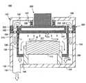
そこで,本実施形態では,各電極111,120と処理空間107の周囲を囲む筒状壁を設け,この筒状壁の外側に上部電極120と天井壁105との間の上部空間108に回り込んだ処理ガスを直接排気する外側排気流路138を形成する。図1は,上述した各電極111,120と処理空間107の周囲を囲む筒状壁をシールド部材300のシールド側壁310で構成した具体例である。この場合における外側排気流路138は,シールド側壁310と処理室102の側壁103との間に形成されて,排気口132に連通する排気空間によって構成される。 Therefore, in the present embodiment, a cylindrical wall surrounding the
これによれば,排気部136の真空ポンプが駆動されることによって,上部電極120の上部空間108に回り込んだ処理ガスは外側排気流路138を通って排気口132から直接排気される。また,このようなシールド側壁310を設けて外側排気流路138を形成するという簡単な構成で,上部電極120の上部空間108に回り込んだ処理ガスを効率よく排気できる。 According to this, when the vacuum pump of the
シールド部材300は例えば図2に示すように構成される。シールド部材300は,シールド側壁310と,その上部に設けられたフランジ320により構成される。シールド側壁310とフランジ320とは一体で形成してもよく,また別体で形成してもよい。 The
シールド部材300はフランジ320によって処理室102の側壁103上部に支持される。具体的にはフランジ320はシールド側壁310の外周面から外側に突出するように形成される。このフランジ320は図1に示すように側壁103と天井壁105との間に挟んでボルトなどで取り付けられる。フランジ320には,処理室102の側壁103との間及び天井壁105との間で気密を保持するため,図示しないOリングなどのシール部材が設けられている。 The
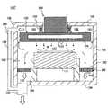
フランジ320には,図2に示すようにシールド側壁310の外周に沿って溝部322が設けられている。溝部322の底部324には上部電極120の上部空間108を外側排気流路138に連通する複数の連通孔326が設けられている。この連通孔326の数や形状を変えることによって,外側排気流路138のコンダクタンスを調整することができる。なお,外側排気流路138を通じた排気効率を高めるためには外側排気流路138のコンダクタンスは,少なくとも上部電極120とシールド側壁310の隙間のコンダクタンスより大きくすることが好ましい。 As shown in FIG. 2, the
なお,図2では連通孔326の形状を丸孔にした例を挙げているが,これに限られるものではなく,例えばスリット,楕円などでもよい。また,連通孔326をスリットで構成する場合は,放射状に延びるスリットでもよく,また円周方向に延びるスリットでもよい。このように,連通孔326の数や形状を調整するだけで,外側排気流路138のコンダクタンスと上部電極120とシールド側壁310の隙間のコンダクタンスとの差を大きくすることができる。これにより,上部電極120の上部空間108に回り込んだ処理ガスの排出効率をより高めることができる。 In addition, although the example which made the shape of the communicating
シールド側壁310の内側,すなわちシールド側壁310と筒状保持部106との間には排気口132と連通する内側排気流路330が形成される。内側排気流路330と排気口132との間にはバッフル板340が設けられている。具体的にはバッフル板340は例えば図1に示すようにシールド側壁310の下端に,筒状保持部106を囲むように設けられる。バッフル板340には多数の貫通孔342が形成されている。これにより,排気部136の真空ポンプが駆動されることによって,シールド側壁310内の雰囲気は内側排気流路330を通って,バッフル板340の貫通孔342を介して排気口132から排気される。 Inside the
シールド側壁310の内面は,陽極酸化処理(例えばアルマイト処理)が施されており,パーティクルが付着し難いようになっている。このようなシールド側壁310で処理空間107を囲むことにより,処理室102の側壁103をパーティクルなどから保護することができる。 The inner surface of the
次に,このようなプラズマ処理装置100の排気の流れを説明する図面を参照しながら説明する。図3は外側排気流路138を形成するシールド部材300を設けた本実施形態にかかるプラズマ処理装置100の概略を示す断面図であり,図4は外側排気流路138を形成しないシールド部材300’を設けた比較例にかかるプラズマ処理装置100’の概略を示す断面図である。図3,図4では,上部電極昇降機構200の構成や下部電極111近傍の構成などを簡略化したものである。 Next, an explanation will be given with reference to the drawings for explaining the flow of the exhaust gas of the
図3,図4のいずれの場合においても,図1に示す排気部136の真空ポンプが駆動されながら,上部電極120から処理空間107に向けて処理ガスが導入される。下部電極111に第1及び第2高周波が印加されると,処理空間107に処理ガスのプラズマが形成され,ウエハWのプラズマ処理が行われる。 3 and 4, the processing gas is introduced from the
このとき,シールド側壁310,310’の内側の雰囲気のほとんどは,内側排気流路330を通ってバッフル板340の貫通孔342を介して排気口132から排出される。ところが,シールド側壁310,310’の内側の雰囲気の一部は,上部電極120の側面の外側に形成される隙間から上部電極120の上部空間108に入り込む。こうして,上部電極120の上部空間108に処理ガス109が回り込んでしまう。 At this time, most of the atmosphere inside the
この場合,もし図4のように外側排気流路138を有しない場合は,上記のように上部電極120の上部空間108に入り込んだ処理ガスは極めて排気され難く残留し易いのに対して,図3のように外側排気流路138を有する場合は,上部電極120の上部空間108に入り込んだ処理ガスを外側排気流路138を通じて直接排気口132から容易に排気させることができる。これにより,上部電極120の上部空間108に処理ガスが残留することを防止できる。また,上部電極120の上部空間108を低圧に保持できるので,上部空間108での異常放電を防止できる。 In this case, if the outer
さらに,シールド側壁310の連通孔326の数や形状を調整して,外側排気流路138のコンダクタンスを上部電極120の外側の隙間(処理ガスが入り込む隙間)よりも大きくすることで,上部電極120の上部空間108に回り込んだ処理ガスを排気口132からより排気させ易くすることができる。 Further, by adjusting the number and shape of the communication holes 326 in the
なお,シールド部材300の構成は,図2に示すものに限られるものではない。例えば図5に示すように,シールド側壁310にフランジ320の溝部322の空間を上部電極120とシールド側壁310との隙間に連通する連通孔312を設けてもよい。これによれば,図6に示すように上部電極120の外側の隙間に入り込んだ処理ガスも連通孔312,326を介して外側排気流路138に導くことができる。これにより,シールド側壁310内の処理ガスが上部電極120の上部空間108に回り込むことを防止できる。 The configuration of the
この連通孔312の数や形状は図5に示すものに限られるものではない。図5では連通孔326の形状を丸孔にした例を挙げているが,例えばスリット,楕円などでもよい。また,連通孔312をスリットで構成する場合は,放射状に延びるスリットでもよく,また円周方向に延びるスリットでもよい。 The number and shape of the communication holes 312 are not limited to those shown in FIG. FIG. 5 shows an example in which the shape of the
また,上記実施形態では,シールド側壁310を各電極120,111と処理空間107の周りを囲む筒状壁とし,このシールド側壁310と処理室102の側壁103との間に外側排気流路138を設けた場合を例に挙げて説明したが,これに限られるものではない。例えば図7に示すように外側排気流路138を,上部電極120の上部空間108を処理室102の排気管134に連通するバイパス配管により構成してもよい。 In the above embodiment, the
図7は,図4に示すプラズマ処理装置100’に外側排気流路138を構成するバイパス配管350を設けた場合の具体例である。これによれば,上部電極120の上部空間108に入り込んだ処理ガスを外側排気流路138であるバイパス配管350を通じて直接排気口132から容易に排気させることができる。これによっても,上部電極120の上部空間108には処理ガスが残留することを防止できる。 FIG. 7 is a specific example in the case where the
また,外側排気流路138を構成するバイパス配管350は図8に示すようにシールド側壁310を設けないプラズマ処理装置100”にも適用できる。この場合,処理室102の側壁103が各電極120,111と処理空間107の周りを囲む筒状壁に相当する。これによっても,上部電極120の上部空間108には処理ガスが残留することを防止できる。 Further, the
以上,添付図面を参照しながら本発明の好適な実施形態について説明したが,本発明は係る例に限定されないことは言うまでもない。当業者であれば,特許請求の範囲に記載された範疇内において,各種の変更例または修正例に想到し得ることは明らかであり,それらについても当然に本発明の技術的範囲に属するものと了解される。 As mentioned above, although preferred embodiment of this invention was described referring an accompanying drawing, it cannot be overemphasized that this invention is not limited to the example which concerns. It will be apparent to those skilled in the art that various changes and modifications can be made within the scope of the claims, and these are naturally within the technical scope of the present invention. Understood.
例えば上記実施形態では,本発明を下部電極のみに2種類の高周波電力を重畳して印加してプラズマを生起させるタイプのプラズマ処理装置に適用した場合を例に挙げて説明したが,これに限定されるものではなく,別のタイプ例えば下部電極のみに1種類の高周波電力を印加するタイプや2種類の高周波電力を上部電極と下部電極にそれぞれ印加するタイプのプラズマ処理装置に適用してもよい。 For example, in the above-described embodiment, the case where the present invention is applied to a plasma processing apparatus of a type in which plasma is generated by applying two types of high-frequency power superimposed on only the lower electrode has been described as an example. The present invention may be applied to other types of plasma processing apparatuses, for example, a type in which only one type of high frequency power is applied to the lower electrode, or a type in which two types of high frequency power are applied to the upper electrode and the lower electrode, respectively. .
本発明は,処理室内において昇降自在な上部電極を備えるプラズマ処理装置に適用可能である。 The present invention is applicable to a plasma processing apparatus including an upper electrode that can be raised and lowered in a processing chamber.
100,100’,100” プラズマ処理装置
102 処理室
102a 孔
103 側壁
104 底壁
105 天井壁
106 筒状保持部
107 処理空間
108 上部空間
109 残留した処理ガス
110 載置台
111 下部電極
112 静電チャック
114 静電チャック電極
115 直流電源
116 冷媒室
118 伝熱ガス供給ライン
119 フォーカスリング
120 上部電極
122 ベローズ
122a,122b フランジ
123 吐出孔
124 電極板
125 電極支持体
126 ガス導入口
127 ガス供給管
128 バルブ
129 マスフローコントローラ
130 処理ガス供給部
132 排気口
134 排気管
136 排気部
138 外側排気流路
140 電力供給装置
142 第1高周波電力供給機構
144 第1フィルタ
146 第1整合器
148 第1電源
152 第2高周波電力供給機構
154 第2フィルタ
156 第2整合器
158 第2電源
160 制御部
162 操作部
164 記憶部
200 上部電極昇降機構
300,300’ シールド部材
310,310’ シールド側壁
312,326 連通孔
320 フランジ
322 溝部
324 底部
330 内側排気流路
340 バッフル板
342 貫通孔
350 バイパス配管
W ウエハ
100, 100 ', 100 "
Claims (2)
Translated fromJapanese前記処理室の底壁に設けられ,前記基板を載置する下部電極と,
前記下部電極に対向して設けられ,載置された前記基板に向けて処理ガスを導入する多数の吹出孔を設けた上部電極と,
前記電極間に前記処理ガスのプラズマを形成する高周波電力を印加する電力供給部と,
前記処理室の天井壁に設けられ,前記天井壁と前記下部電極との間で前記上部電極を昇降させる昇降機構と,
前記各電極とその間の処理空間の周囲を囲む筒状壁と,
前記筒状壁の内側に設けられ,前記処理空間の雰囲気を排気する内側排気流路と,
前記筒状壁の外側に設けられ,前記上部電極と前記天井壁との間の空間に回り込んだ処理ガスを排気する外側排気流路と,
前記筒状壁の上部に設けられ,前記外側排気流路を塞ぐように張り出したフランジ部と,を備え,
前記フランジ部の上側には前記筒状壁の外周に沿って溝部を設け,
前記溝部の底部には前記外側排気流路を前記上部電極と前記天井壁との間の空間に連通する連通孔を設けるとともに,前記溝部の側部には前記上部電極と前記筒状壁との隙間が形成される部位に、その隙間に前記外側排気流路を連通する連通孔を設けたことを特徴とするプラズマ処理装置。A plasma processing apparatus for performing predetermined plasma processing on a substrate in a processing chamber,
A lower electrode provided on the bottom wall of the processing chamber and on which the substrate is placed;
An upper electrode provided opposite to the lower electrode and provided with a plurality of blowing holes for introducing a processing gas toward the mounted substrate;
Apower supply unit for applying a high-frequency power to form a plasma of the processing gas between the electrodes,
An elevating mechanism provided on the ceiling wall of the processing chamber and elevating and lowering the upper electrode between the ceiling wall and the lower electrode;
A cylindrical wall surrounding each electrode and the processing space between them;
An inner exhaust passage provided inside the cylindrical wall and exhausting the atmosphere of the processing space;
An outer exhaust passage that is provided outside the cylindrical wall and exhausts the processing gas that has entered the space between the upper electrode and the ceiling wall;
A flange portion provided at an upper portion of the cylindrical wall and projecting so as to close the outer exhaust flow path;
A groove is provided on the upper side of the flange along the outer periphery of the cylindrical wall,
The bottom of the groove is provided with a communication hole that communicates the outer exhaust flow path with the space between the upper electrode and the ceiling wall. A plasma processing apparatus, wherein a communication hole that communicates the outer exhaust flow path is provided in a portion where a gap is formed .
前記外側排気流路は,前記処理室の側壁と前記シールド側壁との間に形成した排気空間であることを特徴とする請求項1に記載のプラズマ処理装置。The cylindrical wall is a shield side wall provided inside the side wall of the processing chamber,
The plasma processing apparatus according to claim 1, wherein the outer exhaust flow path is an exhaust space formed between a side wall of the processing chamber and the shield side wall.
Priority Applications (6)
| Application Number | Priority Date | Filing Date | Title |
|---|---|---|---|
| JP2010119547AJP5567392B2 (en) | 2010-05-25 | 2010-05-25 | Plasma processing equipment |
| US13/114,101US8858754B2 (en) | 2010-05-25 | 2011-05-24 | Plasma processing apparatus |
| TW100118041ATWI522014B (en) | 2010-05-25 | 2011-05-24 | Plasma processing device |
| EP11004262.9AEP2390897B1 (en) | 2010-05-25 | 2011-05-24 | Plasma processing apparatus |
| CN201110146665.XACN102262999B (en) | 2010-05-25 | 2011-05-25 | Plasma treatment device |
| KR1020110049361AKR101737014B1 (en) | 2010-05-25 | 2011-05-25 | Plasma processing apparatus |
Applications Claiming Priority (1)
| Application Number | Priority Date | Filing Date | Title |
|---|---|---|---|
| JP2010119547AJP5567392B2 (en) | 2010-05-25 | 2010-05-25 | Plasma processing equipment |
Publications (2)
| Publication Number | Publication Date |
|---|---|
| JP2011249470A JP2011249470A (en) | 2011-12-08 |
| JP5567392B2true JP5567392B2 (en) | 2014-08-06 |
Family
ID=44117156
Family Applications (1)
| Application Number | Title | Priority Date | Filing Date |
|---|---|---|---|
| JP2010119547AActiveJP5567392B2 (en) | 2010-05-25 | 2010-05-25 | Plasma processing equipment |
Country Status (6)
| Country | Link |
|---|---|
| US (1) | US8858754B2 (en) |
| EP (1) | EP2390897B1 (en) |
| JP (1) | JP5567392B2 (en) |
| KR (1) | KR101737014B1 (en) |
| CN (1) | CN102262999B (en) |
| TW (1) | TWI522014B (en) |
Families Citing this family (76)
| Publication number | Priority date | Publication date | Assignee | Title |
|---|---|---|---|---|
| JP5445252B2 (en)* | 2010-03-16 | 2014-03-19 | 東京エレクトロン株式会社 | Deposition equipment |
| JP5567392B2 (en)* | 2010-05-25 | 2014-08-06 | 東京エレクトロン株式会社 | Plasma processing equipment |
| US8906160B2 (en)* | 2010-12-23 | 2014-12-09 | Intermolecular, Inc. | Vapor based processing system with purge mode |
| JP5902896B2 (en)* | 2011-07-08 | 2016-04-13 | 東京エレクトロン株式会社 | Substrate processing equipment |
| TW201325326A (en) | 2011-10-05 | 2013-06-16 | Applied Materials Inc | Plasma processing equipment and substrate support assembly thereof |
| US9928987B2 (en) | 2012-07-20 | 2018-03-27 | Applied Materials, Inc. | Inductively coupled plasma source with symmetrical RF feed |
| US9082590B2 (en) | 2012-07-20 | 2015-07-14 | Applied Materials, Inc. | Symmetrical inductively coupled plasma source with side RF feeds and RF distribution plates |
| US10249470B2 (en) | 2012-07-20 | 2019-04-02 | Applied Materials, Inc. | Symmetrical inductively coupled plasma source with coaxial RF feed and coaxial shielding |
| US9449794B2 (en) | 2012-07-20 | 2016-09-20 | Applied Materials, Inc. | Symmetrical inductively coupled plasma source with side RF feeds and spiral coil antenna |
| US9896769B2 (en) | 2012-07-20 | 2018-02-20 | Applied Materials, Inc. | Inductively coupled plasma source with multiple dielectric windows and window-supporting structure |
| US10170279B2 (en) | 2012-07-20 | 2019-01-01 | Applied Materials, Inc. | Multiple coil inductively coupled plasma source with offset frequencies and double-walled shielding |
| US9132436B2 (en) | 2012-09-21 | 2015-09-15 | Applied Materials, Inc. | Chemical control features in wafer process equipment |
| JP2014082354A (en)* | 2012-10-17 | 2014-05-08 | Hitachi High-Technologies Corp | Plasma processing apparatus |
| US10256079B2 (en) | 2013-02-08 | 2019-04-09 | Applied Materials, Inc. | Semiconductor processing systems having multiple plasma configurations |
| WO2014149200A1 (en) | 2013-03-15 | 2014-09-25 | Applied Materials, Inc. | Plasma reactor with highly symmetrical four-fold gas injection |
| JP2015090916A (en)* | 2013-11-06 | 2015-05-11 | 東京エレクトロン株式会社 | Substrate processing apparatus and substrate processing method |
| CN103646841B (en)* | 2013-11-22 | 2016-01-27 | 上海华力微电子有限公司 | A kind of plasma etch apparatus |
| KR101560623B1 (en)* | 2014-01-03 | 2015-10-15 | 주식회사 유진테크 | Substrate processing apparatus and substrate processing method |
| US9852905B2 (en)* | 2014-01-16 | 2017-12-26 | Taiwan Semiconductor Manufacturing Company, Ltd. | Systems and methods for uniform gas flow in a deposition chamber |
| JP2015142016A (en)* | 2014-01-29 | 2015-08-03 | 東京エレクトロン株式会社 | substrate processing apparatus |
| JP6438320B2 (en)* | 2014-06-19 | 2018-12-12 | 東京エレクトロン株式会社 | Plasma processing equipment |
| US11637002B2 (en) | 2014-11-26 | 2023-04-25 | Applied Materials, Inc. | Methods and systems to enhance process uniformity |
| JP6423706B2 (en)* | 2014-12-16 | 2018-11-14 | 東京エレクトロン株式会社 | Plasma processing equipment |
| US20160225652A1 (en) | 2015-02-03 | 2016-08-04 | Applied Materials, Inc. | Low temperature chuck for plasma processing systems |
| US10167552B2 (en)* | 2015-02-05 | 2019-01-01 | Lam Research Ag | Spin chuck with rotating gas showerhead |
| US9741593B2 (en) | 2015-08-06 | 2017-08-22 | Applied Materials, Inc. | Thermal management systems and methods for wafer processing systems |
| US10504700B2 (en) | 2015-08-27 | 2019-12-10 | Applied Materials, Inc. | Plasma etching systems and methods with secondary plasma injection |
| US10157755B2 (en)* | 2015-10-01 | 2018-12-18 | Lam Research Corporation | Purge and pumping structures arranged beneath substrate plane to reduce defects |
| US10763082B2 (en)* | 2016-03-04 | 2020-09-01 | Taiwan Semiconductor Manufacturing Co., Ltd. | Chamber of plasma system, liner for plasma system and method for installing liner to plasma system |
| WO2017169556A1 (en)* | 2016-03-30 | 2017-10-05 | 東京エレクトロン株式会社 | Plasma electrode and plasma processing device |
| JP6394641B2 (en)* | 2016-04-25 | 2018-09-26 | トヨタ自動車株式会社 | Plasma device |
| US10504754B2 (en) | 2016-05-19 | 2019-12-10 | Applied Materials, Inc. | Systems and methods for improved semiconductor etching and component protection |
| KR102553629B1 (en)* | 2016-06-17 | 2023-07-11 | 삼성전자주식회사 | Plasma processing apparatus |
| US9865484B1 (en) | 2016-06-29 | 2018-01-09 | Applied Materials, Inc. | Selective etch using material modification and RF pulsing |
| US10546729B2 (en) | 2016-10-04 | 2020-01-28 | Applied Materials, Inc. | Dual-channel showerhead with improved profile |
| CN106373868B (en)* | 2016-10-10 | 2020-03-10 | 昆山龙腾光电股份有限公司 | Manufacturing method of array substrate |
| US10559451B2 (en)* | 2017-02-15 | 2020-02-11 | Applied Materials, Inc. | Apparatus with concentric pumping for multiple pressure regimes |
| USD838681S1 (en)* | 2017-04-28 | 2019-01-22 | Applied Materials, Inc. | Plasma chamber liner |
| USD837754S1 (en)* | 2017-04-28 | 2019-01-08 | Applied Materials, Inc. | Plasma chamber liner |
| USD842259S1 (en)* | 2017-04-28 | 2019-03-05 | Applied Materials, Inc. | Plasma chamber liner |
| US11276590B2 (en) | 2017-05-17 | 2022-03-15 | Applied Materials, Inc. | Multi-zone semiconductor substrate supports |
| JP7176860B6 (en) | 2017-05-17 | 2022-12-16 | アプライド マテリアルズ インコーポレイテッド | Semiconductor processing chamber to improve precursor flow |
| US11276559B2 (en) | 2017-05-17 | 2022-03-15 | Applied Materials, Inc. | Semiconductor processing chamber for multiple precursor flow |
| US10297458B2 (en) | 2017-08-07 | 2019-05-21 | Applied Materials, Inc. | Process window widening using coated parts in plasma etch processes |
| JP6896565B2 (en)* | 2017-08-25 | 2021-06-30 | 東京エレクトロン株式会社 | Inner wall and substrate processing equipment |
| US11670490B2 (en)* | 2017-09-29 | 2023-06-06 | Taiwan Semiconductor Manufacturing Co., Ltd. | Integrated circuit fabrication system with adjustable gas injector |
| US11328909B2 (en) | 2017-12-22 | 2022-05-10 | Applied Materials, Inc. | Chamber conditioning and removal processes |
| CN111630637B (en)* | 2018-01-26 | 2024-10-01 | 东京毅力科创株式会社 | Substrate processing apparatus |
| US10964512B2 (en) | 2018-02-15 | 2021-03-30 | Applied Materials, Inc. | Semiconductor processing chamber multistage mixing apparatus and methods |
| US10319600B1 (en) | 2018-03-12 | 2019-06-11 | Applied Materials, Inc. | Thermal silicon etch |
| US10699879B2 (en) | 2018-04-17 | 2020-06-30 | Applied Materials, Inc. | Two piece electrode assembly with gap for plasma control |
| CN108588818A (en)* | 2018-04-17 | 2018-09-28 | 陕西飞米企业管理合伙企业(有限合伙) | A kind of exhaust collection ring in vapor deposition equipment |
| KR102516885B1 (en)* | 2018-05-10 | 2023-03-30 | 삼성전자주식회사 | Deposition equipment and method of fabricating semiconductor device using the same |
| CN108987235B (en)* | 2018-07-12 | 2020-06-05 | 昆山龙腾光电股份有限公司 | Plasma processing device |
| US11049755B2 (en) | 2018-09-14 | 2021-06-29 | Applied Materials, Inc. | Semiconductor substrate supports with embedded RF shield |
| US11062887B2 (en) | 2018-09-17 | 2021-07-13 | Applied Materials, Inc. | High temperature RF heater pedestals |
| US11417534B2 (en) | 2018-09-21 | 2022-08-16 | Applied Materials, Inc. | Selective material removal |
| US11682560B2 (en) | 2018-10-11 | 2023-06-20 | Applied Materials, Inc. | Systems and methods for hafnium-containing film removal |
| CN109195297B (en)* | 2018-10-23 | 2020-09-18 | 山东大学 | A precisely adjustable dielectric barrier discharge device and method |
| US11121002B2 (en) | 2018-10-24 | 2021-09-14 | Applied Materials, Inc. | Systems and methods for etching metals and metal derivatives |
| CN208835019U (en)* | 2018-11-12 | 2019-05-07 | 江苏鲁汶仪器有限公司 | Reaction chamber inner lining |
| US11437242B2 (en) | 2018-11-27 | 2022-09-06 | Applied Materials, Inc. | Selective removal of silicon-containing materials |
| JP7477515B2 (en)* | 2019-01-08 | 2024-05-01 | アプライド マテリアルズ インコーポレイテッド | Pumping apparatus and method for a substrate processing chamber - Patents.com |
| JP2020147795A (en)* | 2019-03-13 | 2020-09-17 | 東京エレクトロン株式会社 | Plasma treatment apparatus |
| CN112309807B (en)* | 2019-08-02 | 2022-12-30 | 中微半导体设备(上海)股份有限公司 | Plasma etching equipment |
| CN112447474B (en)* | 2019-09-04 | 2022-11-04 | 中微半导体设备(上海)股份有限公司 | Plasma processor with movable ring |
| JP7378276B2 (en)* | 2019-11-12 | 2023-11-13 | 東京エレクトロン株式会社 | plasma processing equipment |
| JP7422531B2 (en)* | 2019-12-17 | 2024-01-26 | 東京エレクトロン株式会社 | Plasma processing equipment and plasma processing method |
| JP7446145B2 (en)* | 2020-04-07 | 2024-03-08 | 東京エレクトロン株式会社 | Substrate processing equipment |
| US20220051912A1 (en)* | 2020-08-12 | 2022-02-17 | Taiwan Semiconductor Manufacturing Company Limited | Gas flow control during semiconductor fabrication |
| US20220084845A1 (en)* | 2020-09-17 | 2022-03-17 | Applied Materials, Inc. | High conductance process kit |
| US11427910B2 (en)* | 2020-10-20 | 2022-08-30 | Sky Tech Inc. | Atomic layer deposition equipment capable of reducing precursor deposition and atomic layer deposition process method using the same |
| CN114582691B (en)* | 2020-11-18 | 2025-02-14 | 中微半导体设备(上海)股份有限公司 | A plasma processing device and a method for adjusting the same |
| JP7600018B2 (en)* | 2021-03-30 | 2024-12-16 | 東京エレクトロン株式会社 | SUBSTRATE PROCESSING APPARATUS AND SUBSTRATE PROCESSING METHOD |
| JP7633205B2 (en)* | 2022-04-04 | 2025-02-19 | 東京エレクトロン株式会社 | Plasma Processing Equipment |
| CN115312368B (en)* | 2022-07-22 | 2025-06-24 | 北京北方华创微电子装备有限公司 | Upper electrode assembly and semiconductor processing equipment |
Family Cites Families (79)
| Publication number | Priority date | Publication date | Assignee | Title |
|---|---|---|---|---|
| NL287968A (en)* | 1962-03-15 | |||
| JPS6289330A (en)* | 1985-10-16 | 1987-04-23 | Hitachi Ltd | processing equipment |
| KR970003885B1 (en)* | 1987-12-25 | 1997-03-22 | 도오교오 에레구토론 가부시끼 가이샤 | Etching method and apparatus |
| JPH0246723A (en)* | 1988-08-09 | 1990-02-16 | Fujitsu Ltd | Thin film forming equipment |
| DE3914065A1 (en)* | 1989-04-28 | 1990-10-31 | Leybold Ag | DEVICE FOR CARRYING OUT PLASMA ETCHING PROCESSES |
| US5084125A (en)* | 1989-09-12 | 1992-01-28 | Matsushita Electric Industrial Co., Ltd. | Apparatus and method for producing semiconductor substrate |
| JPH03145124A (en) | 1989-10-31 | 1991-06-20 | Fujitsu Ltd | dry etching equipment |
| DE4025396A1 (en)* | 1990-08-10 | 1992-02-13 | Leybold Ag | DEVICE FOR PRODUCING A PLASMA |
| JP2939355B2 (en)* | 1991-04-22 | 1999-08-25 | 東京エレクトロン株式会社 | Plasma processing equipment |
| FR2682047B1 (en)* | 1991-10-07 | 1993-11-12 | Commissariat A Energie Atomique | GAS PHASE CHEMICAL PROCESSING REACTOR. |
| US5238532A (en)* | 1992-02-27 | 1993-08-24 | Hughes Aircraft Company | Method and apparatus for removal of subsurface damage in semiconductor materials by plasma etching |
| US5376224A (en)* | 1992-02-27 | 1994-12-27 | Hughes Aircraft Company | Method and apparatus for non-contact plasma polishing and smoothing of uniformly thinned substrates |
| US5292400A (en)* | 1992-03-23 | 1994-03-08 | Hughes Aircraft Company | Method and apparatus for producing variable spatial frequency control in plasma assisted chemical etching |
| US5372674A (en)* | 1993-05-14 | 1994-12-13 | Hughes Aircraft Company | Electrode for use in a plasma assisted chemical etching process |
| JP3452617B2 (en)* | 1993-12-10 | 2003-09-29 | 真空冶金株式会社 | Gas deposition equipment |
| TW295677B (en)* | 1994-08-19 | 1997-01-11 | Tokyo Electron Co Ltd | |
| JPH08199364A (en) | 1995-01-27 | 1996-08-06 | Kokusai Electric Co Ltd | CVD apparatus and processing method |
| TW323387B (en)* | 1995-06-07 | 1997-12-21 | Tokyo Electron Co Ltd | |
| JP3536585B2 (en) | 1997-04-25 | 2004-06-14 | 松下電器産業株式会社 | Workpiece plasma processing apparatus and plasma processing method |
| JP2000349078A (en)* | 1999-06-03 | 2000-12-15 | Mitsubishi Electric Corp | Chemical vapor deposition apparatus and method for manufacturing semiconductor device |
| JP3662779B2 (en)* | 1999-06-22 | 2005-06-22 | シャープ株式会社 | Plasma processing equipment |
| JP2001057359A (en)* | 1999-08-17 | 2001-02-27 | Tokyo Electron Ltd | Plasma processing device |
| KR100638916B1 (en)* | 2000-05-17 | 2006-10-25 | 동경 엘렉트론 주식회사 | Processing unit and its maintenance method |
| JP3667202B2 (en)* | 2000-07-13 | 2005-07-06 | 株式会社荏原製作所 | Substrate processing equipment |
| JP4602532B2 (en)* | 2000-11-10 | 2010-12-22 | 東京エレクトロン株式会社 | Plasma processing equipment |
| KR100516844B1 (en)* | 2001-01-22 | 2005-09-26 | 동경 엘렉트론 주식회사 | Device and method for treatment |
| JP4672169B2 (en)* | 2001-04-05 | 2011-04-20 | キヤノンアネルバ株式会社 | Plasma processing equipment |
| US6527911B1 (en)* | 2001-06-29 | 2003-03-04 | Lam Research Corporation | Configurable plasma volume etch chamber |
| US20030024900A1 (en)* | 2001-07-24 | 2003-02-06 | Tokyo Electron Limited | Variable aspect ratio plasma source |
| KR100431660B1 (en)* | 2001-07-24 | 2004-05-17 | 삼성전자주식회사 | Dry Etching Apparatus for Manufacturing Semiconductor Devices |
| US20030042227A1 (en)* | 2001-08-29 | 2003-03-06 | Tokyo Electron Limited | Apparatus and method for tailoring an etch profile |
| JP4137419B2 (en) | 2001-09-28 | 2008-08-20 | 東京エレクトロン株式会社 | Plasma processing equipment |
| US20030092278A1 (en)* | 2001-11-13 | 2003-05-15 | Fink Steven T. | Plasma baffle assembly |
| JP4186536B2 (en)* | 2002-07-18 | 2008-11-26 | 松下電器産業株式会社 | Plasma processing equipment |
| KR100426816B1 (en)* | 2002-07-31 | 2004-04-14 | 삼성전자주식회사 | Plasma processing equipment having improved vacuum pressure control apparatus |
| US7780786B2 (en)* | 2002-11-28 | 2010-08-24 | Tokyo Electron Limited | Internal member of a plasma processing vessel |
| US7009281B2 (en)* | 2003-03-14 | 2006-03-07 | Lam Corporation | Small volume process chamber with hot inner surfaces |
| JP4173389B2 (en)* | 2003-03-19 | 2008-10-29 | 東京エレクトロン株式会社 | Plasma processing equipment |
| US20040261712A1 (en)* | 2003-04-25 | 2004-12-30 | Daisuke Hayashi | Plasma processing apparatus |
| JP4399219B2 (en) | 2003-09-19 | 2010-01-13 | 東京エレクトロン株式会社 | Plasma processing apparatus and upper electrode unit |
| JP4286576B2 (en) | 2003-04-25 | 2009-07-01 | 東京エレクトロン株式会社 | Plasma processing equipment |
| JP4399206B2 (en)* | 2003-08-06 | 2010-01-13 | 株式会社アルバック | Thin film manufacturing equipment |
| JP4607517B2 (en)* | 2003-09-03 | 2011-01-05 | 東京エレクトロン株式会社 | Plasma processing equipment |
| WO2005117083A1 (en) | 2004-05-27 | 2005-12-08 | Tokyo Electron Limited | Substrate processing apparatus |
| US20060000552A1 (en)* | 2004-07-05 | 2006-01-05 | Tokyo Electron Limited | Plasma processing apparatus and cleaning method thereof |
| US7708834B2 (en)* | 2004-11-02 | 2010-05-04 | Tokyo Electron Limited | Bolt and plasma processing apparatus provided with same |
| KR100790392B1 (en)* | 2004-11-12 | 2008-01-02 | 삼성전자주식회사 | Semiconductor manufacturing device |
| WO2006106665A1 (en)* | 2005-03-31 | 2006-10-12 | Tokyo Electron Limited | Method for nitriding substrate and method for forming insulating film |
| JP4509864B2 (en)* | 2005-05-30 | 2010-07-21 | 東京エレクトロン株式会社 | Plasma processing method and plasma processing apparatus |
| US7850778B2 (en)* | 2005-09-06 | 2010-12-14 | Lemaire Charles A | Apparatus and method for growing fullerene nanotube forests, and forming nanotube films, threads and composite structures therefrom |
| KR101172997B1 (en)* | 2005-09-22 | 2012-08-09 | 도쿄엘렉트론가부시키가이샤 | Plasma processing apparatus |
| US7825018B2 (en)* | 2006-02-28 | 2010-11-02 | Tokyo Electron Limited | Plasma oxidation method and method for manufacturing semiconductor device |
| US8006640B2 (en)* | 2006-03-27 | 2011-08-30 | Tokyo Electron Limited | Plasma processing apparatus and plasma processing method |
| JP5425361B2 (en)* | 2006-07-28 | 2014-02-26 | 東京エレクトロン株式会社 | Plasma surface treatment method, plasma treatment method, and plasma treatment apparatus |
| JP4961948B2 (en)* | 2006-10-27 | 2012-06-27 | 東京エレクトロン株式会社 | Plasma processing apparatus, plasma processing method, and storage medium |
| KR100823302B1 (en)* | 2006-12-08 | 2008-04-17 | 주식회사 테스 | Plasma processing equipment |
| KR100978754B1 (en)* | 2008-04-03 | 2010-08-30 | 주식회사 테스 | Plasma processing equipment |
| US20080202689A1 (en)* | 2006-12-08 | 2008-08-28 | Tes Co., Ltd. | Plasma processing apparatus |
| US7943007B2 (en)* | 2007-01-26 | 2011-05-17 | Lam Research Corporation | Configurable bevel etcher |
| JP2008270595A (en)* | 2007-04-23 | 2008-11-06 | Texas Instr Japan Ltd | Reaction product delamination prevention structure and manufacturing method thereof, and manufacturing method of semiconductor device using the structure |
| US7807222B2 (en)* | 2007-09-17 | 2010-10-05 | Asm International N.V. | Semiconductor processing parts having apertures with deposited coatings and methods for forming the same |
| JP5249547B2 (en)* | 2007-09-28 | 2013-07-31 | 東京エレクトロン株式会社 | Plasma processing apparatus and gas exhaust method thereof |
| JP5032269B2 (en)* | 2007-11-02 | 2012-09-26 | 東京エレクトロン株式会社 | Temperature adjusting apparatus and temperature adjusting method for substrate to be processed, and plasma processing apparatus including the same |
| JP5548841B2 (en)* | 2008-01-16 | 2014-07-16 | チャーム エンジニアリング シーオー エルティーディー | Substrate processing equipment |
| US20090188625A1 (en)* | 2008-01-28 | 2009-07-30 | Carducci James D | Etching chamber having flow equalizer and lower liner |
| JP5264231B2 (en)* | 2008-03-21 | 2013-08-14 | 東京エレクトロン株式会社 | Plasma processing equipment |
| JP5222598B2 (en)* | 2008-03-25 | 2013-06-26 | 東京エレクトロン株式会社 | Plasma processing apparatus and power supply rod |
| US7987814B2 (en)* | 2008-04-07 | 2011-08-02 | Applied Materials, Inc. | Lower liner with integrated flow equalizer and improved conductance |
| JP5102706B2 (en)* | 2008-06-23 | 2012-12-19 | 東京エレクトロン株式会社 | Baffle plate and substrate processing apparatus |
| JP5086192B2 (en)* | 2008-07-01 | 2012-11-28 | 東京エレクトロン株式会社 | Plasma processing equipment |
| JP5357487B2 (en)* | 2008-09-30 | 2013-12-04 | 東京エレクトロン株式会社 | Silicon oxide film forming method, computer-readable storage medium, and plasma oxidation processing apparatus |
| JP5075793B2 (en)* | 2008-11-06 | 2012-11-21 | 東京エレクトロン株式会社 | Movable gas introduction structure and substrate processing apparatus |
| JP5643528B2 (en)* | 2009-03-30 | 2014-12-17 | 東京エレクトロン株式会社 | Substrate processing equipment |
| JP5292160B2 (en)* | 2009-03-31 | 2013-09-18 | 東京エレクトロン株式会社 | Gas flow path structure and substrate processing apparatus |
| JP5551420B2 (en)* | 2009-12-04 | 2014-07-16 | 東京エレクトロン株式会社 | Substrate processing apparatus, method for measuring distance between electrodes thereof, and storage medium for storing program |
| JP2011171450A (en)* | 2010-02-17 | 2011-09-01 | Nuflare Technology Inc | Film deposition apparatus and method |
| JP2011192664A (en)* | 2010-03-11 | 2011-09-29 | Tokyo Electron Ltd | Plasma etching method and plasma etching apparatus |
| JP5782226B2 (en)* | 2010-03-24 | 2015-09-24 | 東京エレクトロン株式会社 | Substrate processing equipment |
| JP5567392B2 (en)* | 2010-05-25 | 2014-08-06 | 東京エレクトロン株式会社 | Plasma processing equipment |
- 2010
- 2010-05-25JPJP2010119547Apatent/JP5567392B2/enactiveActive
- 2011
- 2011-05-24EPEP11004262.9Apatent/EP2390897B1/enactiveActive
- 2011-05-24TWTW100118041Apatent/TWI522014B/enactive
- 2011-05-24USUS13/114,101patent/US8858754B2/enactiveActive
- 2011-05-25KRKR1020110049361Apatent/KR101737014B1/enactiveActive
- 2011-05-25CNCN201110146665.XApatent/CN102262999B/enactiveActive
Also Published As
| Publication number | Publication date |
|---|---|
| KR101737014B1 (en) | 2017-05-17 |
| US20110290419A1 (en) | 2011-12-01 |
| JP2011249470A (en) | 2011-12-08 |
| TW201216788A (en) | 2012-04-16 |
| KR20110129356A (en) | 2011-12-01 |
| EP2390897A2 (en) | 2011-11-30 |
| US8858754B2 (en) | 2014-10-14 |
| CN102262999B (en) | 2014-01-01 |
| TWI522014B (en) | 2016-02-11 |
| CN102262999A (en) | 2011-11-30 |
| EP2390897A3 (en) | 2014-04-30 |
| EP2390897B1 (en) | 2019-08-21 |
Similar Documents
| Publication | Publication Date | Title |
|---|---|---|
| JP5567392B2 (en) | Plasma processing equipment | |
| US9460893B2 (en) | Substrate processing apparatus | |
| KR102432446B1 (en) | Mounting table and plasma processing apparatus | |
| TWI663686B (en) | Substrate support providing gap height and planarization adjustment in plasma processing chamber | |
| KR102664176B1 (en) | Plasma processing apparatus | |
| KR102414566B1 (en) | Apparatus and method for etching substrate | |
| KR102621517B1 (en) | Substrate processing apparatus | |
| US11495445B2 (en) | Plasma processing apparatus and plasma processing method | |
| KR101922811B1 (en) | Substrate processing apparatus | |
| KR20200051505A (en) | Placing table and substrate processing apparatus | |
| JP5596265B2 (en) | Vacuum processing equipment | |
| US20200312623A1 (en) | Substrate processing apparatus and substrate processing method | |
| KR102554732B1 (en) | Inner wall and substrate treatment device | |
| US20230335381A1 (en) | Substrate processing apparatus | |
| TWI533389B (en) | Airtight module and exhaust method of the airtight module | |
| KR102767880B1 (en) | Substrate processing apparatus and substrate processing method | |
| KR20250091537A (en) | ESC control device and substrate treating apparatus including the same | |
| KR20250091540A (en) | Showerhead unit and substrate treating apparatus including the same | |
| KR20250091536A (en) | Baffle control device and substrate treating apparatus including the same | |
| WO2025033203A1 (en) | Substrate processing device | |
| KR20250088984A (en) | Ring control device and substrate treating apparatus including the same | |
| WO2024142187A1 (en) | Plasma processing device |
Legal Events
| Date | Code | Title | Description |
|---|---|---|---|
| A621 | Written request for application examination | Free format text:JAPANESE INTERMEDIATE CODE: A621 Effective date:20130412 | |
| A977 | Report on retrieval | Free format text:JAPANESE INTERMEDIATE CODE: A971007 Effective date:20131227 | |
| A131 | Notification of reasons for refusal | Free format text:JAPANESE INTERMEDIATE CODE: A131 Effective date:20140110 | |
| A521 | Request for written amendment filed | Free format text:JAPANESE INTERMEDIATE CODE: A523 Effective date:20140221 | |
| TRDD | Decision of grant or rejection written | ||
| A01 | Written decision to grant a patent or to grant a registration (utility model) | Free format text:JAPANESE INTERMEDIATE CODE: A01 Effective date:20140603 | |
| A61 | First payment of annual fees (during grant procedure) | Free format text:JAPANESE INTERMEDIATE CODE: A61 Effective date:20140619 | |
| R150 | Certificate of patent or registration of utility model | Ref document number:5567392 Country of ref document:JP Free format text:JAPANESE INTERMEDIATE CODE: R150 | |
| R250 | Receipt of annual fees | Free format text:JAPANESE INTERMEDIATE CODE: R250 | |
| R250 | Receipt of annual fees | Free format text:JAPANESE INTERMEDIATE CODE: R250 | |
| R250 | Receipt of annual fees | Free format text:JAPANESE INTERMEDIATE CODE: R250 | |
| R250 | Receipt of annual fees | Free format text:JAPANESE INTERMEDIATE CODE: R250 | |
| R250 | Receipt of annual fees | Free format text:JAPANESE INTERMEDIATE CODE: R250 | |
| R250 | Receipt of annual fees | Free format text:JAPANESE INTERMEDIATE CODE: R250 | |
| R250 | Receipt of annual fees | Free format text:JAPANESE INTERMEDIATE CODE: R250 |