JP5562917B2 - Semiconductor device and manufacturing method thereof - Google Patents
Semiconductor device and manufacturing method thereofDownload PDFInfo
- Publication number
- JP5562917B2 JP5562917B2JP2011203847AJP2011203847AJP5562917B2JP 5562917 B2JP5562917 B2JP 5562917B2JP 2011203847 AJP2011203847 AJP 2011203847AJP 2011203847 AJP2011203847 AJP 2011203847AJP 5562917 B2JP5562917 B2JP 5562917B2
- Authority
- JP
- Japan
- Prior art keywords
- semiconductor substrate
- layer
- forming
- electrode
- semiconductor
- Prior art date
- Legal status (The legal status is an assumption and is not a legal conclusion. Google has not performed a legal analysis and makes no representation as to the accuracy of the status listed.)
- Active
Links
Images


Classifications
- H—ELECTRICITY
- H10—SEMICONDUCTOR DEVICES; ELECTRIC SOLID-STATE DEVICES NOT OTHERWISE PROVIDED FOR
- H10D—INORGANIC ELECTRIC SEMICONDUCTOR DEVICES
- H10D30/00—Field-effect transistors [FET]
- H10D30/60—Insulated-gate field-effect transistors [IGFET]
- H10D30/64—Double-diffused metal-oxide semiconductor [DMOS] FETs
- H10D30/66—Vertical DMOS [VDMOS] FETs
- H10D30/668—Vertical DMOS [VDMOS] FETs having trench gate electrodes, e.g. UMOS transistors
- H—ELECTRICITY
- H01—ELECTRIC ELEMENTS
- H01L—SEMICONDUCTOR DEVICES NOT COVERED BY CLASS H10
- H01L21/00—Processes or apparatus adapted for the manufacture or treatment of semiconductor or solid state devices or of parts thereof
- H01L21/02—Manufacture or treatment of semiconductor devices or of parts thereof
- H01L21/04—Manufacture or treatment of semiconductor devices or of parts thereof the devices having potential barriers, e.g. a PN junction, depletion layer or carrier concentration layer
- H01L21/18—Manufacture or treatment of semiconductor devices or of parts thereof the devices having potential barriers, e.g. a PN junction, depletion layer or carrier concentration layer the devices having semiconductor bodies comprising elements of Group IV of the Periodic Table or AIIIBV compounds with or without impurities, e.g. doping materials
- H01L21/22—Diffusion of impurity materials, e.g. doping materials, electrode materials, into or out of a semiconductor body, or between semiconductor regions; Interactions between two or more impurities; Redistribution of impurities
- H01L21/225—Diffusion of impurity materials, e.g. doping materials, electrode materials, into or out of a semiconductor body, or between semiconductor regions; Interactions between two or more impurities; Redistribution of impurities using diffusion into or out of a solid from or into a solid phase, e.g. a doped oxide layer
- H01L21/2251—Diffusion into or out of group IV semiconductors
- H01L21/2254—Diffusion into or out of group IV semiconductors from or through or into an applied layer, e.g. photoresist, nitrides
- H01L21/2257—Diffusion into or out of group IV semiconductors from or through or into an applied layer, e.g. photoresist, nitrides the applied layer being silicon or silicide or SIPOS, e.g. polysilicon, porous silicon
- H—ELECTRICITY
- H10—SEMICONDUCTOR DEVICES; ELECTRIC SOLID-STATE DEVICES NOT OTHERWISE PROVIDED FOR
- H10D—INORGANIC ELECTRIC SEMICONDUCTOR DEVICES
- H10D30/00—Field-effect transistors [FET]
- H10D30/01—Manufacture or treatment
- H10D30/021—Manufacture or treatment of FETs having insulated gates [IGFET]
- H10D30/028—Manufacture or treatment of FETs having insulated gates [IGFET] of double-diffused metal oxide semiconductor [DMOS] FETs
- H10D30/0291—Manufacture or treatment of FETs having insulated gates [IGFET] of double-diffused metal oxide semiconductor [DMOS] FETs of vertical DMOS [VDMOS] FETs
- H10D30/0295—Manufacture or treatment of FETs having insulated gates [IGFET] of double-diffused metal oxide semiconductor [DMOS] FETs of vertical DMOS [VDMOS] FETs using recessing of the source electrodes
- H—ELECTRICITY
- H10—SEMICONDUCTOR DEVICES; ELECTRIC SOLID-STATE DEVICES NOT OTHERWISE PROVIDED FOR
- H10D—INORGANIC ELECTRIC SEMICONDUCTOR DEVICES
- H10D30/00—Field-effect transistors [FET]
- H10D30/01—Manufacture or treatment
- H10D30/021—Manufacture or treatment of FETs having insulated gates [IGFET]
- H10D30/028—Manufacture or treatment of FETs having insulated gates [IGFET] of double-diffused metal oxide semiconductor [DMOS] FETs
- H10D30/0291—Manufacture or treatment of FETs having insulated gates [IGFET] of double-diffused metal oxide semiconductor [DMOS] FETs of vertical DMOS [VDMOS] FETs
- H10D30/0297—Manufacture or treatment of FETs having insulated gates [IGFET] of double-diffused metal oxide semiconductor [DMOS] FETs of vertical DMOS [VDMOS] FETs using recessing of the gate electrodes, e.g. to form trench gate electrodes
- H—ELECTRICITY
- H10—SEMICONDUCTOR DEVICES; ELECTRIC SOLID-STATE DEVICES NOT OTHERWISE PROVIDED FOR
- H10D—INORGANIC ELECTRIC SEMICONDUCTOR DEVICES
- H10D62/00—Semiconductor bodies, or regions thereof, of devices having potential barriers
- H10D62/10—Shapes, relative sizes or dispositions of the regions of the semiconductor bodies; Shapes of the semiconductor bodies
- H10D62/13—Semiconductor regions connected to electrodes carrying current to be rectified, amplified or switched, e.g. source or drain regions
- H10D62/149—Source or drain regions of field-effect devices
- H10D62/151—Source or drain regions of field-effect devices of IGFETs
- H10D62/152—Source regions of DMOS transistors
- H10D62/153—Impurity concentrations or distributions
- H—ELECTRICITY
- H10—SEMICONDUCTOR DEVICES; ELECTRIC SOLID-STATE DEVICES NOT OTHERWISE PROVIDED FOR
- H10D—INORGANIC ELECTRIC SEMICONDUCTOR DEVICES
- H10D62/00—Semiconductor bodies, or regions thereof, of devices having potential barriers
- H10D62/10—Shapes, relative sizes or dispositions of the regions of the semiconductor bodies; Shapes of the semiconductor bodies
- H10D62/17—Semiconductor regions connected to electrodes not carrying current to be rectified, amplified or switched, e.g. channel regions
- H10D62/393—Body regions of DMOS transistors or IGBTs
- H—ELECTRICITY
- H10—SEMICONDUCTOR DEVICES; ELECTRIC SOLID-STATE DEVICES NOT OTHERWISE PROVIDED FOR
- H10D—INORGANIC ELECTRIC SEMICONDUCTOR DEVICES
- H10D62/00—Semiconductor bodies, or regions thereof, of devices having potential barriers
- H10D62/80—Semiconductor bodies, or regions thereof, of devices having potential barriers characterised by the materials
- H10D62/83—Semiconductor bodies, or regions thereof, of devices having potential barriers characterised by the materials being Group IV materials, e.g. B-doped Si or undoped Ge
- H—ELECTRICITY
- H10—SEMICONDUCTOR DEVICES; ELECTRIC SOLID-STATE DEVICES NOT OTHERWISE PROVIDED FOR
- H10D—INORGANIC ELECTRIC SEMICONDUCTOR DEVICES
- H10D64/00—Electrodes of devices having potential barriers
- H10D64/20—Electrodes characterised by their shapes, relative sizes or dispositions
- H10D64/27—Electrodes not carrying the current to be rectified, amplified, oscillated or switched, e.g. gates
- H10D64/311—Gate electrodes for field-effect devices
- H10D64/411—Gate electrodes for field-effect devices for FETs
- H10D64/511—Gate electrodes for field-effect devices for FETs for IGFETs
- H10D64/512—Disposition of the gate electrodes, e.g. buried gates
- H10D64/513—Disposition of the gate electrodes, e.g. buried gates within recesses in the substrate, e.g. trench gates, groove gates or buried gates
- H—ELECTRICITY
- H10—SEMICONDUCTOR DEVICES; ELECTRIC SOLID-STATE DEVICES NOT OTHERWISE PROVIDED FOR
- H10D—INORGANIC ELECTRIC SEMICONDUCTOR DEVICES
- H10D64/00—Electrodes of devices having potential barriers
- H10D64/60—Electrodes characterised by their materials
- H10D64/62—Electrodes ohmically coupled to a semiconductor
- H—ELECTRICITY
- H10—SEMICONDUCTOR DEVICES; ELECTRIC SOLID-STATE DEVICES NOT OTHERWISE PROVIDED FOR
- H10D—INORGANIC ELECTRIC SEMICONDUCTOR DEVICES
- H10D64/00—Electrodes of devices having potential barriers
- H10D64/111—Field plates
- H10D64/117—Recessed field plates, e.g. trench field plates or buried field plates
- H—ELECTRICITY
- H10—SEMICONDUCTOR DEVICES; ELECTRIC SOLID-STATE DEVICES NOT OTHERWISE PROVIDED FOR
- H10D—INORGANIC ELECTRIC SEMICONDUCTOR DEVICES
- H10D64/00—Electrodes of devices having potential barriers
- H10D64/20—Electrodes characterised by their shapes, relative sizes or dispositions
- H10D64/23—Electrodes carrying the current to be rectified, amplified, oscillated or switched, e.g. sources, drains, anodes or cathodes
- H10D64/251—Source or drain electrodes for field-effect devices
- H10D64/256—Source or drain electrodes for field-effect devices for lateral devices wherein the source or drain electrodes are recessed in semiconductor bodies
Landscapes
- Engineering & Computer Science (AREA)
- Physics & Mathematics (AREA)
- Condensed Matter Physics & Semiconductors (AREA)
- General Physics & Mathematics (AREA)
- Manufacturing & Machinery (AREA)
- Computer Hardware Design (AREA)
- Microelectronics & Electronic Packaging (AREA)
- Power Engineering (AREA)
- Electrodes Of Semiconductors (AREA)
- Insulated Gate Type Field-Effect Transistor (AREA)
Description
Translated fromJapanese本発明の実施形態は、半導体装置及びその製造方法に関する。 Embodiments described herein relate generally to a semiconductor device and a method for manufacturing the same.
電力用MOSFET(Metal-Oxide-Semiconductor Field-Effect Transistor:金属酸化物半導体電界効果トランジスタ)においては、オン抵抗を低減させるために、半導体基板にゲート電極を埋め込んだトレンチゲート構造(U−MOS構造)が提案されている。U−MOS構造においては、半導体基板の上面に複数本のゲートトレンチを周期的に形成し、このゲートトレンチ内にゲート電極を埋め込み、半導体基板におけるゲートトレンチ間の領域をソース電極に接触させている。このため、ソース電極に接続させるソース層及びキャリア排出層は、ゲートトレンチ間の領域に形成する必要がある。このとき、ソース層はゲートトレンチの近傍に形成し、キャリア排出層はゲートトレンチから離隔した領域に形成する必要がある。そして、1チップ内に形成する複数のMOSFET間において、閾値及びオン抵抗等の特性が均一になるように、キャリア排出層とゲートトレンチとの距離を均一とする必要がある。 In power MOSFETs (Metal-Oxide-Semiconductor Field-Effect Transistors), a trench gate structure (U-MOS structure) in which a gate electrode is embedded in a semiconductor substrate to reduce on-resistance Has been proposed. In the U-MOS structure, a plurality of gate trenches are periodically formed on the upper surface of a semiconductor substrate, a gate electrode is embedded in the gate trench, and a region between the gate trenches in the semiconductor substrate is in contact with the source electrode. . For this reason, the source layer and the carrier discharge layer connected to the source electrode need to be formed in a region between the gate trenches. At this time, the source layer needs to be formed in the vicinity of the gate trench, and the carrier discharge layer needs to be formed in a region separated from the gate trench. In addition, it is necessary to make the distance between the carrier discharge layer and the gate trench uniform so that characteristics such as a threshold value and on-resistance are uniform among a plurality of MOSFETs formed in one chip.
一方、電力用MOSFETの性能を向上させるためには、U−MOS構造を高集積化することが有効である。しかしながら、ゲートトレンチとキャリア排出層との間の位置合わせ精度の限界により、U−MOS構造の高集積化が制約されている。 On the other hand, in order to improve the performance of the power MOSFET, it is effective to highly integrate the U-MOS structure. However, the high integration of the U-MOS structure is limited by the limit of alignment accuracy between the gate trench and the carrier discharge layer.
実施形態によれば、高集積化が容易な半導体装置及びその製造方法を提供する。 According to the embodiment, a semiconductor device that can be easily integrated and a manufacturing method thereof are provided.
実施形態に係る半導体装置の製造方法は、第1導電形の半導体基板の上面に複数本のトレンチを形成する工程と、前記トレンチの内面上にゲート絶縁膜を形成する工程と、前記トレンチ内の下部にゲート電極を埋め込む工程と、前記トレンチ内の上部に絶縁部材を埋め込む工程と、前記半導体基板の上層部を除去することにより、前記半導体基板の上面から前記絶縁部材を突出させる工程と、前記半導体基板に不純物を導入することにより、前記半導体基板における前記ゲート電極の下端よりも上方の部分に、第2導電形のベース層を形成する工程と、前記突出した絶縁部材を覆うように、マスク膜を形成する工程と、前記ベース層に不純物を導入することにより、前記ベース層の上層部であって下面が前記ゲート電極の上端よりも下方となる部分に、第1導電形の第1半導体層を形成する工程と、前記マスク膜における前記絶縁部材の側面上に形成された部分をマスクとして、前記半導体基板に不純物を注入することにより、前記ベース層の一部及び前記第1半導体層の一部に実効的な不純物濃度が前記ベース層の実効的な不純物濃度よりも高い第2導電形のキャリア排出層を形成する工程と、前記半導体基板の上面に接続されるように第1電極を形成する工程と、前記半導体基板の下面に接続されるように第2電極を形成する工程と、を備える。 A method of manufacturing a semiconductor device according to an embodiment includes a step of forming a plurality of trenches on an upper surface of a first conductivity type semiconductor substrate, a step of forming a gate insulating film on the inner surface of the trench, A step of embedding a gate electrode in a lower portion, a step of embedding an insulating member in an upper portion of the trench, a step of projecting the insulating member from an upper surface of the semiconductor substrate by removing an upper layer portion of the semiconductor substrate, A step of forming a base layer of the second conductivity type in a portion above the lower end of the gate electrode in the semiconductor substrate by introducing impurities into the semiconductor substrate, and a mask so as to cover the protruding insulating member Forming a film and introducing impurities into the base layer, so that the lower surface of the upper layer of the base layer is lower than the upper end of the gate electrode. Forming a first semiconductor layer of a first conductivity type in a portion; and implanting impurities into the semiconductor substrate using a portion formed on a side surface of the insulating member in the mask film as a mask, thereby Forming a second conductivity type carrier discharging layer having an effective impurity concentration higher than an effective impurity concentration of the base layer in a part of the layer and a part of the first semiconductor layer; Forming a first electrode so as to be connected to the upper surface, and forming a second electrode so as to be connected to the lower surface of the semiconductor substrate.
実施形態に係る半導体装置は、上面に複数対の突条部が形成された半導体基板部材と、各対に属する前記突条部間に設けられ、上面が前記突条部の上端よりも下方に位置した絶縁部材と、前記絶縁部材の直下域に設けられたゲート電極と、前記半導体基板部材と前記ゲート電極との間に設けられたゲート絶縁膜と、前記半導体基板部材の上面に接続された第1電極と、前記半導体基板部材の下面に接続された第2電極と、を備える。前記半導体基板部材は、第1導電形であり、前記第2電極に接続され、前記ゲート電極の下端部が進入した第2半導体層と、第2導電形であり、前記第2半導体層上に設けられ、前記ゲート電極が貫通したベース層と、第1導電形であり、前記突条部を構成し、前記第1電極に接続された第1半導体層と、第2導電形であり、前記半導体基板部材の上層部分における前記突条部の対間の領域の直下域に設けられ、前記第1電極に接続され、実効的な不純物濃度が前記ベース層の実効的な不純物濃度よりも高いキャリア排出層と、を有する。 The semiconductor device according to the embodiment is provided between a semiconductor substrate member having a plurality of pairs of protrusions formed on the upper surface and the protrusions belonging to each pair, and the upper surface is below the upper end of the protrusions. An insulating member positioned; a gate electrode provided immediately below the insulating member; a gate insulating film provided between the semiconductor substrate member and the gate electrode; and an upper surface of the semiconductor substrate member A first electrode; and a second electrode connected to the lower surface of the semiconductor substrate member. The semiconductor substrate member is of a first conductivity type, connected to the second electrode, and a second semiconductor layer into which a lower end portion of the gate electrode enters, and a second conductivity type, on the second semiconductor layer A base layer through which the gate electrode passes, and a first conductivity type; a first semiconductor layer that constitutes the protrusion and is connected to the first electrode; and a second conductivity type, Carriers provided in a region directly below the pair of protrusions in the upper layer portion of the semiconductor substrate member, connected to the first electrode, and having an effective impurity concentration higher than the effective impurity concentration of the base layer And an exhaust layer.
以下、図面を参照しつつ、本発明の実施形態について説明する。
先ず、第1の実施形態について説明する。
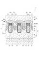
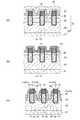
図1は、本実施形態に係る半導体装置を例示する断面図であり、
図2は、横軸に図1に示すA−A’線における位置をとり、縦軸に不純物濃度をとって、ソース層における不純物濃度のプロファイルを例示するグラフ図である。
本実施形態に係る半導体装置は、低耐圧電力用MOSFETである。Hereinafter, embodiments of the present invention will be described with reference to the drawings.
First, the first embodiment will be described.
FIG. 1 is a cross-sectional view illustrating a semiconductor device according to this embodiment.
FIG. 2 is a graph illustrating an impurity concentration profile in the source layer, with the horizontal axis indicating the position along the line AA ′ shown in FIG. 1 and the vertical axis indicating the impurity concentration.
The semiconductor device according to the present embodiment is a low breakdown voltage power MOSFET.
図1に示すように、本実施形態に係る半導体装置1は、半導体基板部材11を有する。半導体基板部材11は、単結晶シリコンにより形成されたシリコン基板上に、シリコンのエピタキシャル層が形成され、その上に多結晶シリコン部材が設けられたものであり、全体が各種の不純物を含むシリコンによって形成されている。半導体基板部材11は、平板状の本体部11aと、本体部11aの上面から突出した複数対の突条部11bとを、一体的に有する。各突条部11bは一方向、すなわち、図1の紙面に対して垂直な方向に延びている。また、隣り合う2本の突条部11bが対をなしている。半導体基板部材11の内部構造及び作製方法は後述する。 As shown in FIG. 1, the
以下、半導体基板部材11以外の構成要素について説明する。
絶縁部材12は、対をなす2本の突条部11bの間に設けられ、絶縁性材料、例えばシリコン酸化物を含む。絶縁部材12は、突条部11bの対毎に設けられており、突条部11bと同じ方向に延びている。絶縁部材12の上面12aは、突条部11bの上端11cよりも下方に位置している。
また、ゲート電極13は、絶縁部材12の直下域に設けられている。ゲート電極13は、導電性材料、例えば、不純物が添加されたポリシリコンを含む。
ゲート電極13は、突条部11bと同じ方向、すなわち突条部11bに対して平行になるように延びている。
ゲート絶縁膜14は、絶縁部材12及びゲート電極13と半導体基板部材11との間に設けられ、絶縁性材料、例えばシリコン酸化物を含む。Hereinafter, components other than the
The
The
The
The
換言すれば、各対の突条部11bの間には、本体部11a内に到達したゲートトレンチ15が形成されており、突条部11bと同じ方向、すなわち、図1の紙面に垂直な方向に延びている。
ゲート絶縁膜14は、ゲートトレンチ15の内面上に形成されている。ゲートトレンチ15内の下部には、ゲート絶縁膜14を介してゲート電極13が埋め込まれており、ゲートトレンチ15内の上部にはゲート絶縁膜14を介して絶縁部材12が埋め込まれている。In other words, the
The
バリアメタル膜16は、半導体基板部材11上に設けられている。バリアメタル膜16は、導電性材料からなり、例えば、チタン層とチタン窒化層との二層膜、又は、チタン層とタングステン層との二層合金膜である。バリアメタル膜16は、半導体基板部材11の上面全体及び絶縁部材12の上面12a全体に接している。バリアメタル膜16上には、金属、例えば、アルミニウムからなる金属膜17が設けられている。バリアメタル膜16及び金属膜17により、ソース電極18(第1電極)が構成されている。一方、半導体基板部材11の下方には、ドレイン電極19(第2電極)が設けられている。ドレイン電極19は例えば金属膜であり、半導体基板部材11の下面全体に接している。 The
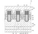
次に、半導体基板部材11の内部構造について説明する。
半導体基板部材11の本体部11aは、その最下層部に、単結晶のシリコンによって形成されたシリコン基板21を有する。シリコン基板21の導電形はn形であり、シリコン基板21の下面はドレイン電極19に接している。
ドリフト層22は、シリコン基板21上に設けられている。ドリフト層22は、シリコン基板21上に成長させたシリコンのエピタキシャル層からなり、その導電形はn形である。但し、ドリフト層22の実効的な不純物濃度は、シリコン基板21の実効的な不純物濃度よりも低い。シリコン基板21及びドリフト層22により、ドレイン層23(第2半導体層)が構成されている。Next, the internal structure of the
The
The
なお、本明細書において「実効的な不純物濃度」とは、半導体材料の導電に寄与する不純物の濃度をいい、例えば、半導体材料にドナーとなる不純物とアクセプタとなる不純物の双方が含有されている場合には、ドナーとアクセプタの相殺分を除いた分の濃度をいう。 In this specification, “effective impurity concentration” refers to the concentration of impurities that contribute to the conductivity of a semiconductor material. For example, the semiconductor material contains both impurities that serve as donors and impurities that serve as acceptors. In this case, the concentration is the concentration excluding the offset between donor and acceptor.
ドリフト層22上には、ベース層24及びキャリア排出層25が設けられている。ベース層24及びキャリア排出層25もエピタキシャル層からなり、その導電形はp形である。但し、キャリア排出層25の実効的な不純物濃度は、ベース層24の実効的な不純物濃度よりも高い。キャリア排出層25は、本体部11aの上層部における突条部11bの直下域の間の領域に配置されており、その上面は本体部11aの上面で露出している。ベース層24は、本体部11aの上層部における突条部11bの直下域及びキャリア排出層25の下方に配置されている。なお、ベース層24は、キャリア排出層25の下端よりも上方に配置されていてもよい。 On the
ソース層26(第1半導体層)は、突条部11bの直下域及び突条部11bに設けられている。ソース層26の下部分26aはエピタキシャル層、すなわち、単結晶のシリコンにより形成され、下部分26aの下部は突条部11bの直下域に配置され、下部分26aの上部は突条部11bの下部を構成している。ソース層26の上部分26bは多結晶のシリコンにより形成され、突条部11bの上部を構成している。ソース層26にはドナーとなる不純物、例えば、リンが含まれている。そして、ソース層26の上部分26bにおけるリン濃度は、下部分26aにおけるリン濃度よりも高い。このため、上部分26bにおける実効的な不純物濃度は、下部分26aにおける実効的な不純物濃度よりも高い。 The source layer 26 (first semiconductor layer) is provided in the region directly below the
そして、ゲート電極13の下端部はドリフト層22内に進入しており、中間部はベース層24を貫通しており、上端部は各対の突条部11bに形成された2つのソース層26の下部分26a間に位置している。ゲート電極13の上端13aは、ベース層24の上面及びキャリア排出層25の上面よりも上方であって、ソース層26の下部分26aの上面よりも下方に位置している。すなわち、上下方向において、ゲート電極13の配設位置は、ドレイン層23、ベース層24及びソース層26の配設位置と重なっている。これにより、半導体装置1においては、ソース層26毎に、nチャネル形のMOSFETが形成される。 The lower end portion of the
図2に実線L1で示すように、ソース層26における上下方向に沿った不純物濃度プロファイルには、下方に向かうときに不純物濃度、すなわちリン濃度が不連続的に減少する点Bが存在し、この点Bは、ソース層26の上部分26bと下部分26aとの界面に相当する。すなわち、実線L1に示す不純物濃度プロファイルにおいて、点Bの上方における不純物濃度は、点Bの下方における不純物濃度よりも十分に高い。具体的には、ソース層26の上部分26bにおけるリン濃度は、上下方向の位置によらず略一定であり、例えば、1×1021cm−3程度である。これに対して、下部分26aにおけるリン濃度は、上端部で最も高く、下方にいくほど低くなる。下部分26aの上端部におけるリン濃度は、例えば、1×1019cm−3程度である。As indicated by a solid line L1 in FIG. 2, the impurity concentration profile along the vertical direction in the
以上説明した半導体装置1によると、ソース電極18に負極の電源電位を印加し、ドレイン電極19に正極の電源電位を印加すると、ドリフト層22とベース層24との界面を起点として空乏層が形成される。この状態で、ゲート電極13に閾値よりも高い電位を印加すると、ベース層24におけるゲート絶縁膜14の近傍に反転層が形成されて、ドレイン電極19から、シリコン基板21、ドリフト層22、ベース層24、ソース層26を介して、電流が流れる。一方、ゲート電極13に閾値よりも低い電位を印加すると、反転層が消滅して電流が遮断される。このとき、半導体基板部材11内で発生した正孔は、キャリア排出層25を介して、速やかにソース電極18に排出される。 According to the
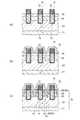
次に、本実施形態に係る半導体装置の製造方法について説明する。
図3(a)〜(c)、図4(a)〜(c)、図5(a)〜(c)及び図6(a)〜(c)は、本実施形態に係る半導体装置の製造方法を例示する工程断面図である。Next, a method for manufacturing the semiconductor device according to the present embodiment will be described.
FIGS. 3A to 3C, FIGS. 4A to 5C, FIGS. 5A to 5C, and FIGS. 6A to 6C illustrate the manufacture of the semiconductor device according to this embodiment. It is process sectional drawing which illustrates a method.
先ず、図3(a)に示すように、単結晶シリコンによって形成されたシリコン基板21を用意する。シリコン基板21には、ドナーとなる不純物、例えば、リンが添加されている。次に、シリコン基板21の上面上にシリコンをエピタキシャル成長させて、エピタキシャル層31を形成する。エピタキシャル層31に添加されたリンの濃度は、シリコン基板21におけるリンの濃度よりも低い。シリコン基板21及びエピタキシャル層31を総称して、半導体基板32という。半導体基板32は単結晶のシリコンからなり、n形の導電形である。 First, as shown in FIG. 3A, a
次に、例えば、熱酸化法又はCVD(Chemical Vapor Deposition:化学気相成長)法により、半導体基板32上にシリコン酸化膜を形成する。次に、リソグラフィ法により、このシリコン酸化膜を選択的に除去して、例えばシリコン酸化物からなるマスク材33を形成する。次に、マスク材33をマスクとしてRIE(Reactive Ion Etching:反応性イオンエッチング)等の異方性エッチングを施すことにより、エピタキシャル層32の上部を選択的に除去して、一方向に延びる複数本のゲートトレンチ15を等間隔に形成する。なお、図3(a)において、ゲートトレンチ15が延びる方向は、紙面に垂直な方向である。その後、マスク材33を除去する。 Next, a silicon oxide film is formed on the
次に、図3(b)に示すように、例えば熱酸化処理を行い、半導体基板32の上面上にゲート絶縁膜14を形成する。ゲート絶縁膜14はゲートトレンチ15の内面上にも形成される。
次に、図3(c)に示すように、全面に、不純物、例えばリンを含有した多結晶シリコンを堆積させる。この多結晶シリコンはゲートトレンチ15内に埋め込まれると共に、半導体基板32の上面上にも堆積する。次に、エッチバックを行い、多結晶シリコンのうち、半導体基板32の上面上に堆積された部分及びゲートトレンチ15内の上部に埋め込まれた部分を除去する。この結果、多結晶シリコンがゲートトレンチ15内の下部のみに残留し、ゲート電極13が形成される。Next, as shown in FIG. 3B, for example, thermal oxidation is performed to form the
Next, as shown in FIG. 3C, polycrystalline silicon containing impurities such as phosphorus is deposited on the entire surface. The polycrystalline silicon is embedded in the
次に、図4(a)に示すように、例えばCVD法により、全面にシリコン酸化物を堆積させて、シリコン酸化膜34を形成する。シリコン酸化膜34は、ゲートトレンチ15内におけるゲート電極13上の部分を埋め込むと共に、半導体基板32の上面上に配置される。
次に、図4(b)に示すように、全面にエッチバックを施し、シリコン酸化膜34及びゲート絶縁膜14のうち、半導体基板32の上面上に形成された部分を除去する。これにより、シリコン酸化膜34がゲートトレンチ15内のみに残留し、絶縁部材12となる。このとき、絶縁部材12の上面12aと半導体基板32の上面32aは、ほぼ同じ高さとなる。Next, as shown in FIG. 4A, a
Next, as shown in FIG. 4B, the entire surface is etched back, and portions of the
次に、図4(c)に示すように、シリコン酸化物に対してシリコンを選択的にエッチングするような条件でエッチバックを行い、半導体基板32の上層部を除去する。これにより、半導体基板32の上面32aが下方に向かって後退し、相対的に、絶縁部材12の大部分及びゲート絶縁膜14の一部が半導体基板32の上面32aから上方に向かって突出する。このとき、上下方向における半導体基板32の上面32aの位置を、ゲート電極13の上端13aの位置に到達しないようにして、上面32aを上端13aよりも上方に位置させる。 Next, as shown in FIG. 4C, etch back is performed under conditions such that silicon is selectively etched with respect to silicon oxide, and the upper layer portion of the
次に、図5(a)に示すように、半導体基板32に対して、上方から、アクセプタとなる不純物、例えばボロンをイオン注入する。これにより、エピタキシャル層31におけるゲート電極13の下端13bよりも上方の部分の導電形が、n形からp形に変化する。このとき、エピタキシャル層31における導電形がp形となった部分が、ベース層24となる。一方、エピタキシャル層31における導電形がn形のまま維持された部分が、ドリフト層22となる。シリコン基板21及びドリフト層22により、ドレイン層23が構成される。 Next, as shown in FIG. 5A, an impurity serving as an acceptor, for example, boron, is ion-implanted into the
次に、図5(b)に示すように、例えばCVD法により、全面に多結晶シリコンを堆積させる。次に、この多結晶シリコン中に、ドナーとなる不純物、例えばリンを導入する。このリンの注入は所謂リンデポ法によって行い、例えば、塩化ホスホリル(オキシ塩化リン)(POCl3)雰囲気中で熱処理を施すことによって行う。これにより、半導体基板32上の全面に、リンが高濃度に導入された多結晶シリコンからなる不純物含有膜35が形成される。不純物含有膜35は、半導体基板32の上面32aに接すると共に、上面32aから突出した絶縁部材12及びゲート絶縁膜14を覆う。Next, as shown in FIG. 5B, polycrystalline silicon is deposited on the entire surface by, eg, CVD. Next, an impurity serving as a donor, for example, phosphorus is introduced into the polycrystalline silicon. The phosphorus is injected by a so-called Lindepo method, for example, by performing a heat treatment in a phosphoryl chloride (phosphorus oxychloride) (POCl3 ) atmosphere. As a result, an impurity-containing
次に、図5(c)に示すように、熱処理を施すことにより、不純物含有膜35に含まれるリンをベース層24内に拡散させる。これにより、ベース層24の上層部の導電形がp形からn形に変化し、n形層36となる。n形層36の下面は、ゲート電極13の上端13aよりも下方に位置させる。 Next, as shown in FIG. 5C, phosphorus contained in the impurity-containing
このとき、n形層36の実効的な不純物濃度は、不純物含有膜35の実効的な不純物濃度よりも低くなる。また、単結晶シリコン中におけるリンの拡散速度は、多結晶シリコン中におけるリンの拡散速度よりも低いため、不純物含有膜35とn形層36の界面において、リンの濃度は不連続的に変化する。更に、n形層36においては、不純物含有膜35から遠ざかるほど、すなわち、下方に向かうほど、リンの濃度が低くなる。 At this time, the effective impurity concentration of the n-
次に、図6(a)に示すように、上方から異方性エッチングを施すことにより、不純物含有膜35における半導体基板32の上面上、並びに絶縁部材12及びゲート絶縁膜14からなる構造体の上面上に形成された部分を除去する。このとき、不純物含有膜35における絶縁部材12及びゲート絶縁膜14からなる構造体の側面上に形成された部分は残留し、側壁37となる。そして、引き続き異方性エッチングを施すことにより、n形層36の上部のうち、側壁37の直下域を除く部分が除去されて、ソーストレンチ38が形成される。 Next, as shown in FIG. 6A, anisotropic etching is performed from above, so that the structure including the insulating
次に、図6(b)に示すように、側壁37、すなわち、不純物含有膜35の残留部分をマスクとして、半導体基板32に対して、アクセプタとなる不純物、例えば、ボロンをイオン注入する。これにより、n形層36及びベース層24における側壁37の直下域間の部分に、導電形がp形であり、実効的な不純物濃度がベース層24の実効的な不純物濃度よりも高いキャリア排出層25が形成される。例えば、加速電圧を2水準としてボロンをイオン注入することにより、キャリア排出層25は、2本の長円柱が上下に連なったような形状となる。なお、不純物含有膜35には1×1021cm−3程度のリンが導入されており、本工程において注入されるボロンの量は1×1019cm−3程度であるから、このボロン注入により不純物含有膜35の導電形がn形からp形に変化することはない。Next, as shown in FIG. 6B, an impurity serving as an acceptor, for example, boron, is ion-implanted into the
このとき、n形層36における導電形がn形のまま維持された部分、すなわち、側壁37の直下域に相当する部分が、ソース層26の下部分26aとなる。一方、側壁37、すなわち、不純物含有膜35の残留部分が、ソース層26の上部分26bとなる。そして、単結晶のシリコンによって形成された半導体基板32の残留部分、及び多結晶のシリコンによって形成された不純物含有膜35の残留部分を総称して、半導体基板部材11という。また、半導体基板部材11のうち、ソーストレンチ38の底面よりも下方に位置する部分を本体部11aとし、上方に位置する部分を突条部11bとする。 At this time, the portion of the n-
次に、図6(c)に示すように、シリコンに対してシリコン酸化物が選択的にエッチングされる条件でエッチバックを行い、絶縁部材12及びゲート絶縁膜14の上部を除去する。これにより、絶縁部材12の上面12aを、側壁37の上端部、すなわち、突条部11bの上端11cよりも下方まで後退させる。 Next, as shown in FIG. 6C, etching back is performed under the condition that silicon oxide is selectively etched with respect to silicon, and the upper portions of the insulating
次に、図1に示すように、半導体基板部材11の上面を覆うように、バリアメタル膜16を形成する。バリアメタル膜16は、ソーストレンチ38内に進入してキャリア排出層25の上面に接触すると共に、ソース層26の露出面全体に接触し、更に、絶縁部材12の上面12a及びゲート絶縁膜14の上端面にも接する。次に、バリアメタル膜16上に金属膜17を成膜する。バリアメタル膜16及び金属膜17により、ソース電極18が構成される。一方、半導体基板部材11の下面上にドレイン電極19を形成する。ドレイン電極19は半導体基板部材11の下面、すなわち、シリコン基板21の下面の全体に接触する。このようにして、半導体装置1が製造される。 Next, as shown in FIG. 1, a
本実施形態では、図3(a)に示す工程において、半導体基板32にゲートトレンチ15を形成し、図4(b)に示す工程において、ゲートトレンチ15内にゲート電極13及び絶縁部材12を形成し、図4(c)に示す工程において、半導体基板32の上面を後退させることにより絶縁部材12を突出させ、図6(a)に示す工程において、突出した絶縁部材12の側面上に側壁37を形成し、図6(b)に示す工程において、側壁37をマスクとしてイオン注入を行うことにより、キャリア排出層25を形成している。 In this embodiment, the
このように、本実施形態によれば、一旦、リソグラフィ法によりゲートトレンチ15を形成した後は、自己整合的な手順によりキャリア排出層25を形成し、ゲートトレンチ15とキャリア排出層25との距離を不純物含有層35の膜厚によって決定することができる。この結果、プロセス条件が変動しても、全てのMOSFET間でゲートトレンチ15とキャリア排出層25との距離を一定に保つことができ、各MOSFETの特性を均一にすることができる。このため、本実施形態に係る半導体装置1は高集積化が容易である。半導体装置1を高集積化することにより、オン抵抗を低減できる。 Thus, according to the present embodiment, after the
これに対して、仮に、ゲートトレンチ15とキャリア排出層25とを別々のリソグラフィ工程によって形成した場合には、ゲートトレンチ15とキャリア排出層25との間に不可避的に合わせずれが発生する。ゲートトレンチ15に対するキャリア排出層25の位置がずれると、MOSFETの特性が変動してしまう。例えば、キャリア排出層25の両側に形成された2つのMOSFETの閾値が相互に異なってしまい、ゲート電極13にオン電位を印加しても、一方のMOSFETがオン状態とならない場合がある。そして、ゲートトレンチ15間の距離が短くなると、ゲートトレンチ15とキャリア排出層25との間の合わせずれが相対的に大きくなるため、ゲートトレンチ15間の距離を短くすることが困難になる。この結果、半導体装置の高集積化が阻害されてしまう。 On the other hand, if the
また、本実施形態では、図5(b)に示す工程において、リンを高濃度に含有した不純物含有膜35を形成し、図5(c)に示す工程において、不純物含有膜35に含まれるリンをベース層24内に拡散させて、n形層36を形成している。そして、図6(a)に示す異方性エッチングの後、不純物含有膜35の残留部分をソース層26の上部分26bとし、n形層36の残留部分をソース層26の下部分26aとしている。これにより、ソース層26の下部分26aのリン濃度をMOSFETに適した所定の値としたまま、ソース層26の上部分26bのリン濃度を高くし、ソース電極18との間の接触抵抗を低減することができる。ソース層26の下部分26aのリン濃度を抑えることにより、チャネル領域、すなわち、ベース層24におけるゲート絶縁膜14の近傍の領域の不純物濃度を抑え、アバランシェ耐量を向上させることができる。 In the present embodiment, the impurity-containing
特に、リンデポ法を用いることにより、不純物含有膜35内にリンを効率よく導入することができる。また、不純物含有膜35を多結晶シリコンにより形成し、ベース層24を単結晶シリコンにより形成することにより、多結晶シリコン中におけるリンの拡散速度と単結晶シリコン中におけるリンの拡散速度との差を利用して、不純物含有膜35のリン濃度とn形層36のリン濃度とを不連続的に大きく異ならせることができる。これにより、上述の効果がより顕著になる。 In particular, phosphorus can be efficiently introduced into the impurity-containing
これに対して、仮に、ソース層26に対するボロンの注入を、1回のイオン注入によって行うと、図2に破線L2で示すように、ソース層26中のリン濃度は上下方向において連続的に変化する。この場合、アバランシェ耐量を確保するためにソース層26の下部分26aのリン濃度を抑えると、上部分26bのリン濃度もあまり高くできないため、ソース電極18との間の接触抵抗が高くなる。 On the other hand, if boron is implanted into the
更に、本実施形態では、図6(a)に示す工程において、異方性エッチングを行うことにより、不純物含有膜35における半導体基板32の上面上に形成された部分を除去している。これにより、図6(b)に示す工程において、ベース層24の上層部に対して、効率的にボロンを注入することができる。この結果、半導体装置1のサステイン耐量が向上する。また、半導体基板32の上面上から不純物含有膜35が除去された後も、異方性エッチングを継続することにより、新たな工程を追加することなく、ソーストレンチ38を自己整合的に形成することができる。ソーストレンチ38を形成することにより、ソース電極18とソース層26との間の接触抵抗を低減することができる。 Furthermore, in this embodiment, in the step shown in FIG. 6A, anisotropic etching is performed to remove a portion of the impurity-containing
更に、本実施形態では、図6(b)に示す工程において、絶縁部材12の上部を除去し、絶縁部材12の上面12aを側壁37の上端部よりも下方に位置させている。これにより、ソーストレンチ38及びその直上域における側壁37等によって挟まれた空間のアスペクト比が低下し、図1に示す工程において、バリアメタル膜16の埋め込みが容易になる。 Furthermore, in the present embodiment, in the step shown in FIG. 6B, the upper portion of the insulating
更にまた、本実施形態では、絶縁部材12の上面12aが、側壁37の上端部、すなわち、ソース層26の上端部よりも下方に位置している。これにより、ソース層26とバリアメタル膜16との接触面積が大きくなり、接触抵抗が低くなる。 Furthermore, in the present embodiment, the
更にまた、本実施形態では、図4(c)に示す工程において、半導体基板32の上面32aを、ゲート電極13の上端部13aよりも上方に位置させている。これにより、リンが高濃度に添加されたソース層26の上部分26aとゲート電極13とが、上下方向において重なることがなくなる。この結果、その後のウェットエッチング等によってゲート絶縁膜14が損傷を受けた場合においても、ソース層26とゲート電極13との間の短絡が生じにくくなり、耐圧が向上する。また、ソース層26とゲート電極13との間の容量を低減することもできる。 Furthermore, in the present embodiment, the
なお、本実施形態においては、ソース層26の上部分26bを多結晶シリコンにより形成する例を示したが、これには限定されない。例えば、上部分26bをエピタキシャル成長させたシリコンによって形成してもよい。また、本実施形態においては、不純物含有膜35をリンデポ法によって形成する例を示したが、これには限定されない。例えば、多結晶シリコンを堆積させた後、リンをイオン注入することにより、不純物含有膜35を形成してもよい。 In the present embodiment, the example in which the
更に、本実施形態においては、図5(c)に示す工程において、不純物含有膜35からベース層24に対して不純物を拡散させることにより、ソース層26の下部分26aを形成する例を示したが、これには限定されない。例えば、上部分26bを形成する多結晶シリコンを堆積させる前に、ベース層24の上層部分に対して不純物をイオン注入して拡散させることにより、下部分26aを形成してもよい。これにより、側壁37(上部分26b)をエピタキシャルシリコン、シリサイド又は金属材料によって形成する場合にも、下部分26bに対して確実に不純物を導入することができる。特に、側壁をシリサイドでない純粋な金属によって形成する場合には、この側壁から不純物を拡散させることは困難であるため、側壁を形成する前に不純物をイオン注入及び拡散させることが必須となる。これらは、後述する他の実施形態においても同様である。 Furthermore, in the present embodiment, an example in which the
次に、第1の実施形態の第1の変形例について説明する。
図7は、本変形例に係る半導体装置を例示する断面図である。
図7に示すように、本変形例に係る半導体装置1aは、前述の第1の実施形態に係る半導体装置1(図1参照)と比較して、不純物含有膜35が側壁37(図1参照)に加工されておらず、半導体基板32の上面上に絶縁部材12の突出部分を覆うように、連続膜として残留している点が異なっている。このため、絶縁部材12は半導体基板部材11内に埋め込まれており、絶縁部材12の上部は半導体基板部材11の突条部内に配置されている。ソース電極18は不純物含有膜35を介してキャリア排出層25に接続される。なお、半導体装置1aにおいては、ドレイン電極19が正極、ソース電極18が負極となるため、p形のキャリア排出層25とn形の不純物含有膜35とのpn界面は順接合となり、通電が阻止されることはない。また、半導体装置1aにおいては、ソーストレンチ38(図1参照)は形成されていない。本変形例における上記以外の構成は、前述の第1の実施形態と同様である。Next, a first modification of the first embodiment will be described.
FIG. 7 is a cross-sectional view illustrating a semiconductor device according to this variation.
As shown in FIG. 7, in the
次に、本変形例に係る半導体装置の製造方法について説明する。
図8は、本変形例に係る半導体装置の製造方法を例示する工程断面図である。
先ず、前述の第1の実施形態と同様に、図3(a)〜図5(c)に示す工程を実施する。Next, a method for manufacturing a semiconductor device according to this modification will be described.
FIG. 8 is a process cross-sectional view illustrating a method for manufacturing a semiconductor device according to this variation.
First, similarly to the above-described first embodiment, the steps shown in FIGS. 3A to 5C are performed.
次に、図8に示すように、不純物含有膜35をエッチバックすることなく、不純物含有膜35越しに、アクセプタとなる不純物、例えば、ボロンをイオン注入する。この場合、前述の第1の実施形態よりも、イオン注入の加速電圧を高くする。このとき、不純物含有膜35における絶縁部材12の側面上に形成された部分は、半導体基板32の上面上に形成された部分と比較して、上下方向における長さが長いため、マスクとして機能する。この結果、n形層36及びベース層24におけるゲートトレンチ15から不純物含有膜35の膜厚分だけ離隔した部分に、キャリア排出層25が形成される。なお、不純物含有膜35には1×1021cm−3程度のリンが導入されており、図8に示す工程において注入されるボロンの量は1×1019cm−3程度であるから、不純物含有膜35の導電形がn形からp形に変化することはない。その後、ソース電極18及びドレイン電極19を形成する。このようにして、本変形例に係る半導体装置1aが製造される。本変形例における上記以外の製造方法は、前述の第1の実施形態と同様である。Next, as shown in FIG. 8, an impurity serving as an acceptor, for example, boron is ion-implanted through the impurity-containing
本変形例においては、不純物含有膜35がソース層26の上部分26bとなる。そして、不純物含有膜35の上面全体がソース電極18に接する。このため、ソース電極18とソース層26との接触面積が大きく、接触抵抗が小さい。
また、不純物含有膜35における絶縁部材12の側面上に形成された部分をマスクとしてボロンをイオン注入することにより、キャリア排出層25を自己整合的に形成することができる。In the present modification, the impurity-containing
In addition, the
更に、前述の第1の実施形態と同様に、不純物含有膜35に含まれるリンをベース層24内に拡散させてn形層36を形成しているため、ソース層26の上部分26bの不純物濃度を高くしてソース電極18との間の接触抵抗を低減できると共に、下部分26aの不純物濃度を抑えてアバランシェ耐量を向上させることができる。更にまた、不純物含有膜35とゲート電極13とを上下方向において離隔させているため、ソース層26とゲート電極13との間の短絡を防止できると共に、容量を低減できる。 Further, since the n-
次に、第1の実施形態の第2の変形例について説明する。
図9は、本変形例に係る半導体装置を例示する断面図である。
図9に示すように、本変形例に係る半導体装置1bは、前述の第1の変形例に係る半導体装置1a(図7参照)と比較して、不純物含有膜35(図7参照)が設けられていない点が異なっている。また、ソース層26に含有されているリンは、不純物含有膜35(図7参照)からの拡散ではなく、イオン注入によって導入されたものである点も異なっている。このため、ソース層26中におけるリン濃度のプロファイルは、前述の第1の実施形態におけるプロファイル(図2参照)とは異なり、例えば、図2に破線L2として示すように、上下方向におけるソース層26の中央部分に1つ以上のピークを持つ。本変形例における上記以外の構成は、前述の第1の変形例と同様である。Next, a second modification of the first embodiment will be described.
FIG. 9 is a cross-sectional view illustrating a semiconductor device according to this variation.
As shown in FIG. 9, the
次に、本変形例に係る半導体装置の製造方法について説明する。
図10(a)〜(c)は、本変形例に係る半導体装置の製造方法を例示する工程断面図である。
先ず、前述の第1の実施形態と同様に、図3(a)〜図5(a)に示す工程を実施する。Next, a method for manufacturing a semiconductor device according to this modification will be described.
10A to 10C are process cross-sectional views illustrating a method for manufacturing a semiconductor device according to this variation.
First, similarly to the first embodiment described above, the steps shown in FIGS. 3A to 5A are performed.
次に、図10(a)に示すように、イオン注入により、ドナーとなる不純物、例えばリンを、ベース層24の上部に対して導入する。これにより、ベース層24の上層部であって下面がゲート電極13の上端13aよりも下方となる部分の導電形がp形からn形に変化し、n形層36となる。
次に、図10(b)に示すように、全面にバリアメタル膜16を成膜する。バリアメタル膜16は、絶縁部材12における半導体基板32の上面から突出した部分も覆うように形成される。Next, as shown in FIG. 10A, an impurity serving as a donor, for example, phosphorus is introduced into the upper portion of the
Next, as shown in FIG. 10B, a
次に、図10(c)に示すように、バリアメタル膜16越しに、アクセプタとなる不純物、例えば、ボロンをイオン注入する。このとき、バリアメタル膜16における絶縁部材12の側面上に形成された部分は、半導体基板32の上面上に形成された部分と比較して、上下方向における長さが長いため、マスクとして機能する。この結果、n形層36及びベース層24におけるゲートトレンチ15からバリアメタル膜16の膜厚分だけ離隔した部分に、キャリア排出層25が形成される。その後、ソース電極18及びドレイン電極19を形成する。このようにして、本変形例に係る半導体装置1bが製造される。本変形例における上記以外の製造方法は、前述の第1の変形例と同様である。 Next, as shown in FIG. 10C, an impurity serving as an acceptor, for example, boron is ion-implanted through the
本変形例においては、バリアメタル膜16における絶縁部材12の側面上に形成された部分をマスクとして使用することにより、キャリア排出層25を自己整合的に形成することができる。 In this modification, the
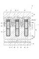
次に、第2の実施形態について説明する。
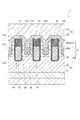
図11は、本実施形態に係る半導体装置を例示する断面図である。
図11に示すように、本実施形態に係る半導体装置2は、前述の第1の実施形態に係る半導体装置1(図1参照)と比較して、絶縁部材12の上面12aが突条部11bの上端11cよりも上方に位置している点が異なっている。このような半導体装置2は、前述の第1の実施形態と同様に、図3(a)〜図6(b)に示す工程を実施した後、図6(c)に示す絶縁部材12の上部を除去する工程を実施せずに、ソース電極18及びドレイン電極19を形成することにより、製造される。本実施形態における上記以外の構成及び製造方法は、前述の第1の実施形態と同様である。Next, a second embodiment will be described.
FIG. 11 is a cross-sectional view illustrating a semiconductor device according to this embodiment.
As shown in FIG. 11, in the
本実施形態においても、前述の第1の実施形態と同様に、側壁37を利用して、キャリア排出層25をゲートトレンチ15に対して自己整合的に形成することができる。また、不純物含有膜35に含まれるリンをベース層24内に拡散させてn形層36を形成しているため、ソース層26の上部分26bの不純物濃度を高くしてソース電極18との間の接触抵抗を低減できると共に、下部分26aの不純物濃度を抑えてアバランシェ耐量を向上させることができる。更に、不純物含有膜35における半導体基板32の上面上に形成された部分を除去しているため、ボロンを効率的に注入することができる。また、新たな工程を追加することなく、ソーストレンチ38を自己整合的に形成することができる。更にまた、ソース層26の上部分26aとゲート電極13とを上下方向において離隔させているため、ソース層26とゲート電極13との間の短絡を防止できると共に、容量を低減できる。 Also in this embodiment, the
次に、第3の実施形態について説明する。
図12は、本実施形態に係る半導体装置を例示する断面図である。
図12に示すように、本実施形態に係る半導体装置3は、前述の第1の実施形態に係る半導体装置1(図1参照)と比較して、ソース層26の上部分26b(図1参照)、すなわち側壁37(図1参照)が設けられておらず、その替わりに、シリサイドからなる側壁41が設けられている点が異なっている。半導体装置3においては、ソース層26は下部分26aのみから構成されている。Next, a third embodiment will be described.
FIG. 12 is a cross-sectional view illustrating a semiconductor device according to this embodiment.
As shown in FIG. 12, the
また、ソース層26の実効的な不純物濃度は、側壁41(シリサイド膜43)の実効的な不純物濃度よりも低い。そして、側壁41及びソース層26における上下方向に沿った不純物濃度プロファイルは、側壁41とソース層26との界面において不純物濃度が不連続的に変化する。この不純物濃度プロファイルの形状は、図2に示すプロファイルと同様である。この場合、図2に示す「上部分26b」は、「側壁41」に置き換えられる。本実施形態における上記以外の構成は、前述の第1の実施形態と同様である。 The effective impurity concentration of the
次に、本実施形態に係る半導体装置の製造方法について説明する。
図13(a)〜(c)は、本実施形態に係る半導体装置の製造方法を例示する工程断面図である。Next, a method for manufacturing the semiconductor device according to the present embodiment will be described.
13A to 13C are process cross-sectional views illustrating the method for manufacturing a semiconductor device according to this embodiment.
先ず、前述の第1の実施形態と同様に、図3(a)〜図5(c)に示す工程を実施する。
次に、図13(a)に示すように、不純物含有膜35上に、例えばチタン又はタングステン等からなる金属膜42を成膜する。
次に、図13(b)に示すように、熱処理を施し、不純物含有膜35に含まれるシリコンと、金属膜42に含まれる金属とを反応させ、シリサイド化させる。これにより、不純物含有膜35がシリサイド膜43に変化する。次に、シリサイド膜43上から、未反応な金属膜42を除去する。First, similarly to the above-described first embodiment, the steps shown in FIGS. 3A to 5C are performed.
Next, as shown in FIG. 13A, a
Next, as shown in FIG. 13B, heat treatment is performed to cause the silicon contained in the impurity-containing
以後の工程は、前述の第1の実施形態と同様である。すなわち、図13(c)に示すように、上方から異方性エッチングを施すことにより、シリサイド膜43における半導体基板32の上面上、並びに絶縁部材12及びゲート絶縁膜14からなる構造体の上面上に形成された部分を除去する。このとき、シリサイド膜43における絶縁部材12及びゲート絶縁膜14からなる構造体の側面上に形成された部分は残留し、側壁41となる。そして、引き続き異方性エッチングを施すことにより、ソーストレンチ38が形成される。次に、側壁41をマスクとして、アクセプタとなる不純物、例えば、ボロンをイオン注入する。これにより、n形層36及びベース層24における側壁41の直下域間の部分に、キャリア排出層25が形成される。 Subsequent steps are the same as those in the first embodiment. That is, as shown in FIG. 13C, by performing anisotropic etching from above, on the upper surface of the
次に、図6(c)に示す工程と同様に、絶縁部材12の上部を除去する。これにより、絶縁部材12の上面12aが側壁41の上端よりも下方に位置する。
次に、図12に示すように、ソース電極18及びドレイン電極19を形成する。このとき、ソース電極18はシリサイドからなる側壁41に接触する。このようにして、本実施形態に係る半導体装置3が製造される。本実施形態における上記以外の製造方法は、前述の第1の実施形態と同様である。Next, similarly to the process shown in FIG. 6C, the upper portion of the insulating
Next, as shown in FIG. 12, the
本実施形態においては、ソース電極18とソース層26との間にシリサイドからなる側壁41が介在しているため、ソース電極18とソース層26との間の抵抗をより一層低減することができる。また、本実施形態においても、前述の第1の実施形態と同様に、側壁41を利用して、キャリア排出層25を自己整合的に形成することができる。また、シリサイド膜43における半導体基板32の上面上に形成された部分を除去しているため、ボロンを効率的に注入することができる。また、新たな工程を追加することなく、ソーストレンチ38を自己整合的に形成することができる。更にまた、側壁41とゲート電極13とを上下方向において離隔させているため、ソース層26とゲート電極13との間の短絡を防止できると共に、容量を低減できる。 In the present embodiment, since the
次に、第3の実施形態の変形例について説明する。
図14は、本変形例に係る半導体装置を例示する断面図である。
図14に示すように、本変形例に係る半導体装置3aは、前述の第3の実施形態に係る半導体装置3(図12参照)と比較して、シリサイド膜43が側壁41(図12参照)に加工されておらず、半導体基板32の上面上に、絶縁部材12の上面を覆うように、連続膜として残留している点が異なっている。このため、ソース電極18はシリサイド膜43を介して、ソース層26及びキャリア排出層25に接続される。また、半導体装置3aにおいては、ソーストレンチ38(図12参照)が形成されていない。本変形例における上記以外の構成は、前述の第3の実施形態と同様である。Next, a modification of the third embodiment will be described.
FIG. 14 is a cross-sectional view illustrating a semiconductor device according to this variation.
As shown in FIG. 14, in the
次に、本変形例に係る半導体装置の製造方法について説明する。
図15は、本変形例に係る半導体装置の製造方法を例示する工程断面図である。
先ず、前述の第3の実施形態と同様に、図3(a)〜図5(c)、図9(a)及び(b)に示す工程を実施する。Next, a method for manufacturing a semiconductor device according to this modification will be described.
FIG. 15 is a process cross-sectional view illustrating a method for manufacturing a semiconductor device according to this variation.
First, similarly to the above-described third embodiment, the steps shown in FIGS. 3A to 5C, FIGS. 9A and 9B are performed.
次に、図15に示すように、シリサイド膜43をエッチバックすることなく、シリサイド膜43越しに、アクセプタとなる不純物、例えば、ボロンをイオン注入する。このイオン注入の際の加速電圧は、前述の第1の実施形態においてボロンをイオン注入する際(図6(b)参照)の加速電圧よりも高くする。このとき、シリサイド膜43における絶縁部材12の側面上に形成された部分は、半導体基板32の上面上に形成された部分と比較して、上下方向、すなわち、イオンの注入方向における長さが長いため、マスクとして機能する。この結果、n形層36及びベース層24におけるゲートトレンチ15からシリサイド膜43の膜厚分だけ離隔した部分に、シリサイド膜43を介してボロンが注入され、キャリア排出層25が形成される。その後、ソース電極18及びドレイン電極19を形成する。このようにして、本変形例に係る半導体装置3aが製造される。本変形例における上記以外の製造方法は、前述の第3の実施形態と同様である。 Next, as shown in FIG. 15, an impurity serving as an acceptor, for example, boron, is ion-implanted through the
本変形例においても、シリサイド膜43における絶縁部材12の側面上に形成された部分をマスクとしてボロンをイオン注入することにより、キャリア排出層25を自己整合的に形成することができる。また、シリサイド膜43とゲート電極13とを上下方向において離隔させているため、ソース層26とゲート電極13との間の短絡を防止できると共に、容量を低減できる。 Also in this modification, the
次に、第4の実施形態について説明する。
図16は、本実施形態に係る半導体装置を例示する断面図である。
図16に示すように、本実施形態に係る半導体装置4は、前述の第1の実施形態に係る半導体装置1(図1参照)と比較して、ゲートトレンチ15内におけるゲート電極13の直下域に、埋込電極46が設けられている点が異なっている。埋込電極46は、導電性材料、例えば、不純物が添加された多結晶シリコンからなり、ソース電極18に接続されている。一方、埋込電極46は、ドレイン電極19及びゲート電極13からは絶縁されている。本実施形態における上記以外の構成は、前述の第1の実施形態と同様である。Next, a fourth embodiment will be described.
FIG. 16 is a cross-sectional view illustrating a semiconductor device according to this embodiment.
As shown in FIG. 16, the
以上説明した実施形態によれば、高集積化が容易な半導体装置及びその製造方法を実現することができる。 According to the embodiments described above, it is possible to realize a semiconductor device that can be easily integrated and a manufacturing method thereof.
以上、本発明のいくつかの実施形態を説明したが、これらの実施形態は、例として提示したものであり、発明の範囲を限定することは意図していない。これら新規な実施形態は、その他の様々な形態で実施されることが可能であり、発明の要旨を逸脱しない範囲で、種々の省略、置き換え、変更を行うことができる。これら実施形態やその変形は、発明の範囲や要旨に含まれるとともに、特許請求の範囲に記載された発明及びその等価物の範囲に含まれる。また、前述の各実施形態は、相互に組み合わせて実施することができる。 As mentioned above, although some embodiment of this invention was described, these embodiment is shown as an example and is not intending limiting the range of invention. These novel embodiments can be implemented in various other forms, and various omissions, replacements, and changes can be made without departing from the scope of the invention. These embodiments and modifications thereof are included in the scope and gist of the invention, and are included in the scope of the invention described in the claims and the equivalents thereof. Further, the above-described embodiments can be implemented in combination with each other.
1、1a、1b、2、3、3a、4:半導体装置、11:半導体基板部材、11a:本体部、11b:突条部、11c:上端、12:絶縁部材、12a:上面、13:ゲート電極、13a:上端、13b:下端、14:ゲート絶縁膜、15:トレンチ、16:バリアメタル膜、17:金属膜、18:ソース電極、19:ドレイン電極、21:シリコン基板、22:ドリフト層、23:ドレイン層、24:ベース層、25:キャリア排出層、26:ソース層、26a:下部分、26b:上部分、31:エピタキシャル層、32:半導体基板、32a:上面、33:マスク材、34:シリコン酸化膜、35:不純物含有膜、36:n形層、37:側壁、38:ソーストレンチ、41:側壁、42:金属膜、43:シリサイド膜、46:埋込電極、B:点、L1:実線、L2:破線1, 1a, 1b, 2, 3, 3a, 4: semiconductor device, 11: semiconductor substrate member, 11a: main body, 11b: protrusion, 11c: upper end, 12: insulating member, 12a: upper surface, 13: gate Electrode, 13a: upper end, 13b: lower end, 14: gate insulating film, 15: trench, 16: barrier metal film, 17: metal film, 18: source electrode, 19: drain electrode, 21: silicon substrate, 22: drift layer , 23: drain layer, 24: base layer, 25: carrier discharge layer, 26: source layer, 26a: lower part, 26b: upper part, 31: epitaxial layer, 32: semiconductor substrate, 32a: upper surface, 33: mask material , 34: silicon oxide film, 35: impurity-containing film, 36: n-type layer, 37: sidewall, 38: source trench, 41: sidewall, 42: metal film, 43: silicide film, 46: buried electrode, : Point, L1: a solid line, L2: the dashed line
Claims (13)
Translated fromJapanese前記トレンチの内面上にゲート絶縁膜を形成する工程と、
前記トレンチ内の下部にゲート電極を埋め込む工程と、
前記トレンチ内の上部に絶縁部材を埋め込む工程と、
前記半導体基板の上層部を除去することにより、前記半導体基板の上面から前記絶縁部材を突出させる工程と、
前記半導体基板に不純物を導入することにより、前記半導体基板における前記ゲート電極の下端よりも上方の部分に、第2導電形のベース層を形成する工程と、
前記突出した絶縁部材を覆うように、マスク膜を形成する工程と、
前記ベース層に不純物を導入することにより、前記ベース層の上層部であって下面が前記ゲート電極の上端よりも下方となる部分に、第1導電形の第1半導体層を形成する工程と、
前記マスク膜における前記絶縁部材の側面上に形成された部分をマスクとして、前記半導体基板に不純物を注入することにより、前記ベース層の一部及び前記第1半導体層の一部に実効的な不純物濃度が前記ベース層の実効的な不純物濃度よりも高い第2導電形のキャリア排出層を形成する工程と、
前記半導体基板の上面に接続されるように第1電極を形成する工程と、
前記半導体基板の下面に接続されるように第2電極を形成する工程と、
を備え、
前記マスク膜を形成する工程は、前記半導体基板の上面に接するように、金属膜を形成する工程を有する半導体装置の製造方法。Forming a plurality of trenches on the upper surface of the semiconductor substrate of the first conductivity type;
Forming a gate insulating film on the inner surface of the trench;
Burying a gate electrode in the lower part of the trench;
Embedding an insulating member in the upper part of the trench;
Removing the upper layer portion of the semiconductor substrate to project the insulating member from the upper surface of the semiconductor substrate;
Forming a second conductivity type base layer in a portion above the lower end of the gate electrode in the semiconductor substrate by introducing impurities into the semiconductor substrate;
Forming a mask film so as to cover the protruding insulating member;
Forming a first-conductivity-type first semiconductor layer in a portion of the upper portion of the base layer, the lower surface of which is below the upper end of the gate electrode, by introducing impurities into the base layer;
By using the portion of the mask film formed on the side surface of the insulating member as a mask, impurities are implanted into the semiconductor substrate, so that an effective impurity is added to a part of the base layer and a part of the first semiconductor layer. Forming a second conductivity type carrier discharge layer having a concentration higher than an effective impurity concentration of the base layer;
Forming a first electrode to be connected to an upper surface of the semiconductor substrate;
Forming a second electrode to be connected to the lower surface of the semiconductor substrate;
Equipped witha,
The step of forming the mask film includes a step of forming a metal film so as to be in contact with the upper surface of the semiconductor substrate .
前記トレンチの内面上にゲート絶縁膜を形成する工程と、
前記トレンチ内の下部にゲート電極を埋め込む工程と、
前記トレンチ内の上部に絶縁部材を埋め込む工程と、
前記半導体基板の上層部を除去することにより、前記半導体基板の上面から前記絶縁部材を突出させる工程と、
前記半導体基板に不純物を導入することにより、前記半導体基板における前記ゲート電極の下端よりも上方の部分に、第2導電形のベース層を形成する工程と、
前記突出した絶縁部材を覆うように、マスク膜を形成する工程と、
前記ベース層に不純物を導入することにより、前記ベース層の上層部であって下面が前記ゲート電極の上端よりも下方となる部分に、第1導電形の第1半導体層を形成する工程と、
前記マスク膜に対して異方性エッチングを施すことにより、前記マスク膜における前記半導体基板の上面上に形成された部分を除去する工程と、
前記マスク膜における前記絶縁部材の側面上に形成された部分をマスクとして、前記半導体基板に不純物を注入することにより、前記ベース層の一部及び前記第1半導体層の一部に実効的な不純物濃度が前記ベース層の実効的な不純物濃度よりも高い第2導電形のキャリア排出層を形成する工程と、
前記絶縁部材の上部を除去することにより、前記絶縁部材の上面を、前記マスク膜における前記絶縁部材の側面上に残留した部分の上端よりも下方の位置まで後退させる工程と、 前記半導体基板の上面に接続されるように第1電極を形成する工程と、
前記半導体基板の下面に接続されるように第2電極を形成する工程と、
を備えた半導体装置の製造方法。Forming a plurality of trenches on the upper surface of the semiconductor substrate of the first conductivity type;
Forming a gate insulating film on the inner surface of the trench;
Burying a gate electrode in the lower part of the trench;
Embedding an insulating member in the upper part of the trench;
Removing the upper layer portion of the semiconductor substrate to project the insulating member from the upper surface of the semiconductor substrate;
Forming a second conductivity type base layer in a portion above the lower end of the gate electrode in the semiconductor substrate by introducing impurities into the semiconductor substrate;
Forming a mask film so as to cover the protruding insulating member;
Forming a first-conductivity-type first semiconductor layer in a portion of the upper portion of the base layer, the lower surface of which is below the upper end of the gate electrode, by introducing impurities into the base layer;
Removing the portion of the mask film formed on the upper surface of the semiconductor substrate by performing anisotropic etching on the mask film;
By using the portion of the mask film formed on the side surface of the insulating member as a mask, impurities are implanted into the semiconductor substrate, so that an effective impurity is added to a part of the base layer and a part of the first semiconductor layer. Forming a second conductivity type carrier discharge layer having a concentration higher than an effective impurity concentration of the base layer;
Removing the upper portion of the insulating member to retract the upper surface of the insulating member to a position below the upper end of the portion of the mask film remaining on the side surface of the insulating member; and the upper surface of the semiconductor substrate Forming a first electrode so as to be connected to
Forming a second electrode to be connected to the lower surface of the semiconductor substrate;
A method for manufacturing a semiconductor device comprising:
前記トレンチの内面上にゲート絶縁膜を形成する工程と、
前記トレンチ内の下部にゲート電極を埋め込む工程と、
前記トレンチ内の上部に絶縁部材を埋め込む工程と、
前記半導体基板の上層部を除去することにより、前記半導体基板の上面から前記絶縁部材を突出させる工程と、
前記半導体基板に不純物を導入することにより、前記半導体基板における前記ゲート電極の下端よりも上方の部分に、第2導電形のベース層を形成する工程と、
前記突出した絶縁部材を覆うように、導電性のマスク膜を形成する工程と、
前記ベース層に不純物を導入することにより、前記ベース層の上層部であって下面が前記ゲート電極の上端よりも下方となる部分に、第1導電形の第1半導体層を形成する工程と、
前記マスク膜における前記絶縁部材の側面上に形成された部分をマスクとして、前記半導体基板に前記マスク膜越しに不純物を注入することにより、前記ベース層の一部及び前記第1半導体層の一部に実効的な不純物濃度が前記ベース層の実効的な不純物濃度よりも高い第2導電形のキャリア排出層を形成する工程と、
前記半導体基板の上面に接続されるように第1電極を形成する工程と、
前記半導体基板の下面に接続されるように第2電極を形成する工程と、
を備えた半導体装置の製造方法。Forming a plurality of trenches on the upper surface of the semiconductor substrate of the first conductivity type;
Forming a gate insulating film on the inner surface of the trench;
Burying a gate electrode in the lower part of the trench;
Embedding an insulating member in the upper part of the trench;
Removing the upper layer portion of the semiconductor substrate to project the insulating member from the upper surface of the semiconductor substrate;
Forming a second conductivity type base layer in a portion above the lower end of the gate electrode in the semiconductor substrate by introducing impurities into the semiconductor substrate;
Forming aconductive mask film so as to cover the protruding insulating member;
Forming a first-conductivity-type first semiconductor layer in a portion of the upper portion of the base layer, the lower surface of which is below the upper end of the gate electrode, by introducing impurities into the base layer;
Using the portion formed on the side surface of the insulating member in the mask film as a mask, by implanting impurities into the semiconductor substrate through themask film, a part of the base layer and a part of the first semiconductor layer Forming a carrier discharge layer of a second conductivity type having an effective impurity concentration higher than that of the base layer;
Forming a first electrode to be connected to an upper surface of the semiconductor substrate;
Forming a second electrode to be connected to the lower surface of the semiconductor substrate;
A method for manufacturing a semiconductor device comprising:
前記トレンチの内面上にゲート絶縁膜を形成する工程と、
前記トレンチ内の下部にゲート電極を埋め込む工程と、
前記トレンチ内の上部に絶縁部材を埋め込む工程と、
前記半導体基板の上層部を除去することにより、前記半導体基板の上面を前記ゲート電極の上端よりも上方に位置させつつ、前記半導体基板の上面から前記絶縁部材を突出させる工程と、
前記半導体基板に不純物を導入することにより、前記半導体基板における前記ゲート電極の下端よりも上方の部分に、第2導電形のベース層を形成する工程と、
前記突出した絶縁部材を覆うように、マスク膜を形成する工程と、
前記ベース層に不純物を導入することにより、前記ベース層の上層部であって下面が前記ゲート電極の上端よりも下方となる部分に、第1導電形の第1半導体層を形成する工程と、
前記マスク膜における前記絶縁部材の側面上に形成された部分をマスクとして、前記半導体基板に不純物を注入することにより、前記ベース層の一部及び前記第1半導体層の一部に実効的な不純物濃度が前記ベース層の実効的な不純物濃度よりも高い第2導電形のキャリア排出層を形成する工程と、
前記半導体基板の上面に接続されるように第1電極を形成する工程と、
前記半導体基板の下面に接続されるように第2電極を形成する工程と、
を備えた半導体装置の製造方法。Forming a plurality of trenches on the upper surface of the semiconductor substrate of the first conductivity type;
Forming a gate insulating film on the inner surface of the trench;
Burying a gate electrode in the lower part of the trench;
Embedding an insulating member in the upper part of the trench;
Removing the upper layer portion of the semiconductor substrate to project the insulating member from the upper surface of the semiconductor substratewhile positioning the upper surface of the semiconductor substrateabove the upper end of the gate electrode ;
Forming a second conductivity type base layer in a portion above the lower end of the gate electrode in the semiconductor substrate by introducing impurities into the semiconductor substrate;
Forming a mask film so as to cover the protruding insulating member;
Forming a first-conductivity-type first semiconductor layer in a portion of the upper portion of the base layer, the lower surface of which is below the upper end of the gate electrode, by introducing impurities into the base layer;
By using the portion of the mask film formed on the side surface of the insulating member as a mask, impurities are implanted into the semiconductor substrate, so that an effective impurity is added to a part of the base layer and a part of the first semiconductor layer. Forming a second conductivity type carrier discharge layer having a concentration higher than an effective impurity concentration of the base layer;
Forming a first electrode to be connected to an upper surface of the semiconductor substrate;
Forming a second electrode to be connected to the lower surface of the semiconductor substrate;
A method for manufacturing a semiconductor device comprising:
前記第1導電層を形成する工程は、前記不純物含有膜に含まれる不純物を前記ベース層内に拡散させる工程を有する請求項2〜4のいずれか1つに記載の半導体装置の製造方法。The step of forming the mask film includes a step of forming an impurity-containing film containing impurities on the semiconductor substrate,
5. The method for manufacturing a semiconductor device accordingto claim2 , wherein the step of forming the first conductive layer includes a step of diffusing impurities contained in the impurity-containing film into the base layer.
前記不純物含有膜上に金属膜を形成する工程と、
前記不純物含有膜と前記金属膜とを反応させてシリサイド化させる工程と、
をさらに有する請求項7記載の半導体装置の製造方法。The step of forming the mask film includes:
Forming a metal film on the impurity-containing film;
Reacting the impurity-containing film with the metal film to form a silicide;
The method of manufacturing a semiconductor device according to claim7 , further comprising:
各対に属する前記突条部間に設けられ、上面が前記突条部の上端よりも下方に位置した絶縁部材と、
前記絶縁部材の直下域に設けられたゲート電極と、
前記半導体基板部材と前記ゲート電極との間に設けられたゲート絶縁膜と、
前記半導体基板部材の上面に接続された第1電極と、
前記半導体基板部材の下面に接続された第2電極と、
を備え、
前記半導体基板部材は、
第1導電形であり、前記第2電極に接続され、前記ゲート電極の下端部が進入した第2半導体層と、
第2導電形であり、前記第2半導体層上に設けられ、前記ゲート電極が貫通したベース層と、
第1導電形であり、前記突条部を構成し、前記第1電極に接続された第1半導体層と、
第2導電形であり、前記半導体基板部材の上層部分における前記突条部の対間の領域の直下域に設けられ、前記第1電極に接続され、実効的な不純物濃度が前記ベース層の実効的な不純物濃度よりも高いキャリア排出層と、
を有した半導体装置。A semiconductor substrate member having a plurality of pairs of protrusions formed on the upper surface;
An insulating member provided between the ridges belonging to each pair, the upper surface of which is located below the upper end of the ridges;
A gate electrode provided immediately below the insulating member;
A gate insulating film provided between the semiconductor substrate member and the gate electrode;
A first electrode connected to an upper surface of the semiconductor substrate member;
A second electrode connected to the lower surface of the semiconductor substrate member;
With
The semiconductor substrate member is
A second semiconductor layer of a first conductivity type, connected to the second electrode and into which a lower end of the gate electrode has entered;
A second conductivity type, provided on the second semiconductor layer, through which the gate electrode penetrates;
A first semiconductor layer of a first conductivity type, constituting the protrusion, and connected to the first electrode;
A second conductivity type, provided immediately below the region between the pair of protrusions in the upper layer portion of the semiconductor substrate member, connected to the first electrode, and having an effective impurity concentration of the base layer Carrier discharge layer higher than typical impurity concentration,
A semiconductor device having
前記トレンチ内に設けられたゲート電極と、
前記半導体基板部材と前記ゲート電極との間に設けられたゲート絶縁膜と、
前記半導体基板部材の上面に接したシリサイド膜と、
前記シリサイド膜の上面に接した第1電極と、
前記半導体基板部材の下面に接続された第2電極と、
を備え、
前記半導体基板部材は、
第1導電形であり、前記第2電極に接続され、前記ゲート電極の下端部が進入した第2半導体層と、
第2導電形であり、前記第2半導体層上に設けられ、前記ゲート電極が貫通したベース層と、
第1導電形であり、実効的な不純物濃度が前記シリサイド膜の実効的な不純物濃度よりも低く、前記ベース層上に設けられ、前記シリサイド膜に接した第1半導体層と、
第2導電形であり、前記トレンチ間であって前記ゲート絶縁膜から離隔した領域に設けられ、前記第1電極に接続され、実効的な不純物濃度が前記ベース層の実効的な不純物濃度よりも高いキャリア排出層と、
を有し、
前記シリサイド膜及び前記第1半導体層における上下方向に沿った不純物濃度プロファイルは、前記シリサイド膜と前記第1半導体層との界面において不純物濃度が不連続的に変化する半導体装置。A semiconductor substrate member made of silicon and having a plurality of trenches formed on the upper surface;
A gate electrode provided in the trench;
A gate insulating film provided between the semiconductor substrate member and the gate electrode;
A silicide film in contact with an upper surface of the semiconductor substrate member;
A first electrode in contact with the upper surface of the silicide film;
A second electrode connected to the lower surface of the semiconductor substrate member;
With
The semiconductor substrate member is
A second semiconductor layer of a first conductivity type, connected to the second electrode and into which a lower end of the gate electrode has entered;
A second conductivity type, provided on the second semiconductor layer, through which the gate electrode penetrates;
A first conductivity type having an effective impurity concentration lower than the effective impurity concentration of the silicide film, provided on the base layer, and in contact with the silicide film;
A second conductivity type, provided in a region between the trenches and separated from the gate insulating film, connected to the first electrode, and having an effective impurity concentration higher than an effective impurity concentration of the base layer; With a high carrier drainage layer,
Have
The impurity concentration profile along the vertical direction in the silicide film and the first semiconductor layer is a semiconductor device in which the impurity concentration changes discontinuously at the interface between the silicide film and the first semiconductor layer.
前記トレンチの上部は各対に属する前記突条部間に形成されており、
前記トレンチの上部内に設けられた絶縁部材をさらに備えた請求項9または10に記載の半導体装置。Plural pairs of protrusions are formed on the upper surface of the semiconductor substrate member,
The upper part of the trench is formed between the protrusions belonging to each pair,
The semiconductor device according to claim9 , further comprising an insulating member provided in an upper portion of the trench.
前記半導体板基部材内に埋め込まれ、上部が各前記突条部内に配置された絶縁部材と、
前記絶縁部材の直下域に設けられたゲート電極と、
前記半導体基板部材と前記ゲート電極との間に設けられたゲート絶縁膜と、
前記半導体基板部材の上面に接続された第1電極と、
前記半導体基板部材の下面に接続された第2電極と、
を備え、
前記半導体基板部材は、
第1導電形であり、前記第2電極に接続され、前記ゲート電極の下端部が進入した第2半導体層と、
第2導電形であり、前記第2半導体層上に設けられ、前記ゲート電極が貫通したベース層と、
第1導電形であり、前記ベース層上に設けられ、前記絶縁部材の上面を覆い、前記第1電極に接した第1半導体層と、
第2導電形であり、前記突条部間の領域の直下域に設けられ、前記第1半導体層及び前記ベース層に接し、実効的な不純物濃度が前記ベース層の実効的な不純物濃度よりも高いキャリア排出層と、
を有した半導体装置。A semiconductor substrate member having a plurality of protrusions formed on the upper surface;
An insulating member embedded in the semiconductor plate base member and having an upper portion disposed in each of the protrusions;
A gate electrode provided immediately below the insulating member;
A gate insulating film provided between the semiconductor substrate member and the gate electrode;
A first electrode connected to an upper surface of the semiconductor substrate member;
A second electrode connected to the lower surface of the semiconductor substrate member;
With
The semiconductor substrate member is
A second semiconductor layer of a first conductivity type, connected to the second electrode and into which a lower end of the gate electrode has entered;
A second conductivity type, provided on the second semiconductor layer, through which the gate electrode penetrates;
A first conductivity type, provided on the base layer, covering a top surface of the insulating member, and in contact with the first electrode;
A second conductivity type, which is provided immediately below the region between the protrusions, is in contact with the first semiconductor layer and the base layer, and an effective impurity concentration is higher than an effective impurity concentration of the base layer; With a high carrier drainage layer,
A semiconductor device having
Priority Applications (6)
| Application Number | Priority Date | Filing Date | Title |
|---|---|---|---|
| JP2011203847AJP5562917B2 (en) | 2011-09-16 | 2011-09-16 | Semiconductor device and manufacturing method thereof |
| TW101108120ATWI463572B (en) | 2011-09-16 | 2012-03-09 | Semiconductor device and manufacturing method thereof |
| US13/420,545US8710582B2 (en) | 2011-09-16 | 2012-03-14 | Semiconductor device and method for manufacturing same |
| CN201210071069.4ACN103000529B (en) | 2011-09-16 | 2012-03-16 | Semiconductor device and its manufacture method |
| US14/195,504US8859365B2 (en) | 2011-09-16 | 2014-03-03 | Semiconductor device and method for manufacturing same |
| US14/485,008US9142667B2 (en) | 2011-09-16 | 2014-09-12 | Semiconductor device and method for manufacturing same |
Applications Claiming Priority (1)
| Application Number | Priority Date | Filing Date | Title |
|---|---|---|---|
| JP2011203847AJP5562917B2 (en) | 2011-09-16 | 2011-09-16 | Semiconductor device and manufacturing method thereof |
Publications (2)
| Publication Number | Publication Date |
|---|---|
| JP2013065724A JP2013065724A (en) | 2013-04-11 |
| JP5562917B2true JP5562917B2 (en) | 2014-07-30 |
Family
ID=47879849
Family Applications (1)
| Application Number | Title | Priority Date | Filing Date |
|---|---|---|---|
| JP2011203847AActiveJP5562917B2 (en) | 2011-09-16 | 2011-09-16 | Semiconductor device and manufacturing method thereof |
Country Status (4)
| Country | Link |
|---|---|
| US (3) | US8710582B2 (en) |
| JP (1) | JP5562917B2 (en) |
| CN (1) | CN103000529B (en) |
| TW (1) | TWI463572B (en) |
Families Citing this family (32)
| Publication number | Priority date | Publication date | Assignee | Title |
|---|---|---|---|---|
| JP5562917B2 (en)* | 2011-09-16 | 2014-07-30 | 株式会社東芝 | Semiconductor device and manufacturing method thereof |
| US8753935B1 (en) | 2012-12-21 | 2014-06-17 | Alpha And Omega Semiconductor Incorporated | High frequency switching MOSFETs with low output capacitance using a depletable P-shield |
| US8951867B2 (en) | 2012-12-21 | 2015-02-10 | Alpha And Omega Semiconductor Incorporated | High density trench-based power MOSFETs with self-aligned active contacts and method for making such devices |
| US8809948B1 (en) | 2012-12-21 | 2014-08-19 | Alpha And Omega Semiconductor Incorporated | Device structure and methods of making high density MOSFETs for load switch and DC-DC applications |
| US9105494B2 (en) | 2013-02-25 | 2015-08-11 | Alpha and Omega Semiconductors, Incorporated | Termination trench for power MOSFET applications |
| TW201443999A (en)* | 2013-05-14 | 2014-11-16 | Anpec Electronics Corp | Ditch type power semiconductor device manufacturing method |
| US9343579B2 (en)* | 2013-05-20 | 2016-05-17 | Semiconductor Energy Laboratory Co., Ltd. | Semiconductor device |
| US8980713B2 (en)* | 2013-05-31 | 2015-03-17 | Sony Corporation | Method for fabricating a metal high-k gate stack for a buried recessed access device |
| US9029974B2 (en)* | 2013-09-11 | 2015-05-12 | Infineon Technologies Ag | Semiconductor device, junction field effect transistor and vertical field effect transistor |
| KR20150051067A (en)* | 2013-11-01 | 2015-05-11 | 삼성전기주식회사 | Power semiconductor device and method of fabricating the same |
| JP2015185646A (en)* | 2014-03-24 | 2015-10-22 | ルネサスエレクトロニクス株式会社 | Semiconductor device |
| CN105070753B (en)* | 2015-07-20 | 2017-11-28 | 东南大学 | A kind of two-way Breakdown Voltage Power semiconductor transistor in longitudinal direction and preparation method thereof |
| CN106898549A (en)* | 2015-12-21 | 2017-06-27 | 株洲南车时代电气股份有限公司 | Trench gate IGBT and trench gate IGBT preparation methods |
| US9960269B2 (en)* | 2016-02-02 | 2018-05-01 | Renesas Electronics Corporation | Semiconductor device and method of manufacturing the same |
| JP6900535B2 (en)* | 2016-03-28 | 2021-07-07 | ローム株式会社 | Semiconductor devices and methods for manufacturing semiconductor devices |
| WO2018052099A1 (en) | 2016-09-14 | 2018-03-22 | 富士電機株式会社 | Reverse conducting insulated-gate bipolar transistor, and production method therefor |
| CN108780814B (en) | 2016-09-14 | 2021-12-21 | 富士电机株式会社 | Semiconductor device and method for manufacturing the same |
| CN108122990B (en)* | 2017-12-26 | 2020-07-17 | 中国科学院微电子研究所 | A reinforced trench-gate power device with enhanced single-event resistance |
| US10714580B2 (en)* | 2018-02-07 | 2020-07-14 | Alpha And Omega Semiconductor (Cayman) Ltd. | Source ballasting for p-channel trench MOSFET |
| JP6958575B2 (en)* | 2019-01-16 | 2021-11-02 | 株式会社デンソー | Semiconductor devices and their manufacturing methods |
| JP6969586B2 (en)* | 2019-04-23 | 2021-11-24 | 株式会社デンソー | Semiconductor devices and their manufacturing methods |
| CN110416211A (en)* | 2019-07-24 | 2019-11-05 | 上海朕芯微电子科技有限公司 | Manufacturing method and structure of a super self-aligned power Trench MOSFET |
| GB2592014B (en)* | 2020-02-11 | 2023-11-15 | Clarksteel Holdings Ltd | Duct termination |
| CN114503280A (en) | 2020-04-16 | 2022-05-13 | 富士电机株式会社 | Semiconductor device and method for manufacturing semiconductor device |
| JP7574558B2 (en) | 2020-07-13 | 2024-10-29 | 富士電機株式会社 | Semiconductor Device |
| US20240055495A1 (en)* | 2020-12-21 | 2024-02-15 | Hitachi Energy Switzerland Ag | Power semiconductor device and method for manufacturing a power semiconductor device |
| CN113410307B (en)* | 2021-04-16 | 2022-10-04 | 深圳真茂佳半导体有限公司 | Field effect transistor structure and its manufacturing method, chip device |
| CN113113473B (en)* | 2021-04-16 | 2022-08-12 | 深圳真茂佳半导体有限公司 | Field effect transistor structure and its manufacturing method, chip device |
| CN117397043A (en)* | 2021-12-27 | 2024-01-12 | 富士电机株式会社 | Semiconductor device |
| JP7742791B2 (en) | 2022-03-11 | 2025-09-22 | ルネサスエレクトロニクス株式会社 | Semiconductor device and manufacturing method thereof |
| JP2024044655A (en)* | 2022-09-21 | 2024-04-02 | 株式会社東芝 | Semiconductor device and its manufacturing method |
| JP2025042663A (en)* | 2023-09-15 | 2025-03-28 | 株式会社東芝 | Semiconductor device, semiconductor device manufacturing method, inverter circuit, drive device, vehicle, and elevator |
Family Cites Families (10)
| Publication number | Priority date | Publication date | Assignee | Title |
|---|---|---|---|---|
| US5323040A (en)* | 1993-09-27 | 1994-06-21 | North Carolina State University At Raleigh | Silicon carbide field effect device |
| GB9815021D0 (en) | 1998-07-11 | 1998-09-09 | Koninkl Philips Electronics Nv | Semiconductor power device manufacture |
| US6921939B2 (en) | 2000-07-20 | 2005-07-26 | Fairchild Semiconductor Corporation | Power MOSFET and method for forming same using a self-aligned body implant |
| US6916745B2 (en) | 2003-05-20 | 2005-07-12 | Fairchild Semiconductor Corporation | Structure and method for forming a trench MOSFET having self-aligned features |
| KR20040079518A (en)* | 2003-03-07 | 2004-09-16 | 삼성전자주식회사 | MOSFET having recessed channel and fabricating method thereof |
| US7652326B2 (en)* | 2003-05-20 | 2010-01-26 | Fairchild Semiconductor Corporation | Power semiconductor devices and methods of manufacture |
| JP2006059940A (en)* | 2004-08-19 | 2006-03-02 | Fuji Electric Device Technology Co Ltd | Semiconductor device |
| US9947770B2 (en) | 2007-04-03 | 2018-04-17 | Vishay-Siliconix | Self-aligned trench MOSFET and method of manufacture |
| JP2012178389A (en) | 2011-02-25 | 2012-09-13 | Renesas Electronics Corp | Semiconductor device |
| JP5562917B2 (en)* | 2011-09-16 | 2014-07-30 | 株式会社東芝 | Semiconductor device and manufacturing method thereof |
- 2011
- 2011-09-16JPJP2011203847Apatent/JP5562917B2/enactiveActive
- 2012
- 2012-03-09TWTW101108120Apatent/TWI463572B/ennot_activeIP Right Cessation
- 2012-03-14USUS13/420,545patent/US8710582B2/enactiveActive
- 2012-03-16CNCN201210071069.4Apatent/CN103000529B/ennot_activeExpired - Fee Related
- 2014
- 2014-03-03USUS14/195,504patent/US8859365B2/ennot_activeExpired - Fee Related
- 2014-09-12USUS14/485,008patent/US9142667B2/ennot_activeExpired - Fee Related
Also Published As
| Publication number | Publication date |
|---|---|
| US8859365B2 (en) | 2014-10-14 |
| US20130069146A1 (en) | 2013-03-21 |
| US20140179075A1 (en) | 2014-06-26 |
| US9142667B2 (en) | 2015-09-22 |
| US20150028413A1 (en) | 2015-01-29 |
| CN103000529B (en) | 2016-01-06 |
| CN103000529A (en) | 2013-03-27 |
| US8710582B2 (en) | 2014-04-29 |
| TW201314791A (en) | 2013-04-01 |
| JP2013065724A (en) | 2013-04-11 |
| TWI463572B (en) | 2014-12-01 |
Similar Documents
| Publication | Publication Date | Title |
|---|---|---|
| JP5562917B2 (en) | Semiconductor device and manufacturing method thereof | |
| US10002952B2 (en) | Silicon carbide semiconductor device and method of manufacturing silicon carbide semiconductor device | |
| CN105264667B (en) | Silicon carbide semiconductor device and manufacturing method thereof | |
| US8174066B2 (en) | Semiconductor device and method of manufacturing semiconductor device | |
| US9379216B2 (en) | Semiconductor device and method for manufacturing same | |
| US20130056790A1 (en) | Semiconductor device and method for manufacturing same | |
| JP2013197551A (en) | Semiconductor device and manufacturing method thereof | |
| JP2007311557A (en) | Semiconductor device and manufacturing method thereof | |
| US8030702B2 (en) | Trenched MOSFET with guard ring and channel stop | |
| US8643095B2 (en) | Semiconductor transistor device and method for manufacturing same | |
| JP2012174989A (en) | Method of manufacturing semiconductor device | |
| US20090267140A1 (en) | Mosfet structure with guard ring | |
| JP2013201267A (en) | Semiconductor device and method of manufacturing the same | |
| US10910493B2 (en) | Semiconductor device and method of manufacturing the same | |
| US20090267143A1 (en) | Trenched mosfet with guard ring and channel stop | |
| US7705399B2 (en) | Semiconductor device with field insulation film formed therein | |
| US20160093731A1 (en) | Method of Manufacturing a Semiconductor Device and Semiconductor Device | |
| US20140124853A1 (en) | Semiconductor device with reduced miller capacitance and fabrication method thereof | |
| KR100929635B1 (en) | Vertical transistor and method of formation thereof | |
| US7723784B2 (en) | Insulated gate semiconductor device and method for manufacturing the same | |
| US9647109B2 (en) | Semiconductor device | |
| JP2012186417A (en) | Semiconductor device and method of manufacturing the same | |
| JP2016076729A (en) | Semiconductor device |
Legal Events
| Date | Code | Title | Description |
|---|---|---|---|
| A621 | Written request for application examination | Free format text:JAPANESE INTERMEDIATE CODE: A621 Effective date:20130902 | |
| A977 | Report on retrieval | Free format text:JAPANESE INTERMEDIATE CODE: A971007 Effective date:20140116 | |
| A131 | Notification of reasons for refusal | Free format text:JAPANESE INTERMEDIATE CODE: A131 Effective date:20140121 | |
| A521 | Request for written amendment filed | Free format text:JAPANESE INTERMEDIATE CODE: A523 Effective date:20140320 | |
| TRDD | Decision of grant or rejection written | ||
| A01 | Written decision to grant a patent or to grant a registration (utility model) | Free format text:JAPANESE INTERMEDIATE CODE: A01 Effective date:20140515 | |
| A61 | First payment of annual fees (during grant procedure) | Free format text:JAPANESE INTERMEDIATE CODE: A61 Effective date:20140611 | |
| R151 | Written notification of patent or utility model registration | Ref document number:5562917 Country of ref document:JP Free format text:JAPANESE INTERMEDIATE CODE: R151 |