JP5554973B2 - Manufacturing method of semiconductor integrated circuit device - Google Patents
Manufacturing method of semiconductor integrated circuit deviceDownload PDFInfo
- Publication number
- JP5554973B2 JP5554973B2JP2009273241AJP2009273241AJP5554973B2JP 5554973 B2JP5554973 B2JP 5554973B2JP 2009273241 AJP2009273241 AJP 2009273241AJP 2009273241 AJP2009273241 AJP 2009273241AJP 5554973 B2JP5554973 B2JP 5554973B2
- Authority
- JP
- Japan
- Prior art keywords
- film
- region
- resist film
- cross
- section
- Prior art date
- Legal status (The legal status is an assumption and is not a legal conclusion. Google has not performed a legal analysis and makes no representation as to the accuracy of the status listed.)
- Expired - Fee Related
Links
Images


Classifications
- H—ELECTRICITY
- H01—ELECTRIC ELEMENTS
- H01L—SEMICONDUCTOR DEVICES NOT COVERED BY CLASS H10
- H01L21/00—Processes or apparatus adapted for the manufacture or treatment of semiconductor or solid state devices or of parts thereof
- H01L21/70—Manufacture or treatment of devices consisting of a plurality of solid state components formed in or on a common substrate or of parts thereof; Manufacture of integrated circuit devices or of parts thereof
- H01L21/71—Manufacture of specific parts of devices defined in group H01L21/70
- H01L21/76—Making of isolation regions between components
- H01L21/762—Dielectric regions, e.g. EPIC dielectric isolation, LOCOS; Trench refilling techniques, SOI technology, use of channel stoppers
- H01L21/76224—Dielectric regions, e.g. EPIC dielectric isolation, LOCOS; Trench refilling techniques, SOI technology, use of channel stoppers using trench refilling with dielectric materials
- H01L21/76229—Concurrent filling of a plurality of trenches having a different trench shape or dimension, e.g. rectangular and V-shaped trenches, wide and narrow trenches, shallow and deep trenches
- H—ELECTRICITY
- H10—SEMICONDUCTOR DEVICES; ELECTRIC SOLID-STATE DEVICES NOT OTHERWISE PROVIDED FOR
- H10B—ELECTRONIC MEMORY DEVICES
- H10B43/00—EEPROM devices comprising charge-trapping gate insulators
- H10B43/10—EEPROM devices comprising charge-trapping gate insulators characterised by the top-view layout
- H—ELECTRICITY
- H10—SEMICONDUCTOR DEVICES; ELECTRIC SOLID-STATE DEVICES NOT OTHERWISE PROVIDED FOR
- H10B—ELECTRONIC MEMORY DEVICES
- H10B43/00—EEPROM devices comprising charge-trapping gate insulators
- H10B43/40—EEPROM devices comprising charge-trapping gate insulators characterised by the peripheral circuit region
- H—ELECTRICITY
- H10—SEMICONDUCTOR DEVICES; ELECTRIC SOLID-STATE DEVICES NOT OTHERWISE PROVIDED FOR
- H10D—INORGANIC ELECTRIC SEMICONDUCTOR DEVICES
- H10D30/00—Field-effect transistors [FET]
- H10D30/60—Insulated-gate field-effect transistors [IGFET]
- H10D30/69—IGFETs having charge trapping gate insulators, e.g. MNOS transistors
- H—ELECTRICITY
- H10—SEMICONDUCTOR DEVICES; ELECTRIC SOLID-STATE DEVICES NOT OTHERWISE PROVIDED FOR
- H10D—INORGANIC ELECTRIC SEMICONDUCTOR DEVICES
- H10D84/00—Integrated devices formed in or on semiconductor substrates that comprise only semiconducting layers, e.g. on Si wafers or on GaAs-on-Si wafers
- H10D84/01—Manufacture or treatment
- H10D84/0123—Integrating together multiple components covered by H10D12/00 or H10D30/00, e.g. integrating multiple IGBTs
- H10D84/0126—Integrating together multiple components covered by H10D12/00 or H10D30/00, e.g. integrating multiple IGBTs the components including insulated gates, e.g. IGFETs
- H10D84/013—Manufacturing their source or drain regions, e.g. silicided source or drain regions
- H10D84/0133—Manufacturing common source or drain regions between multiple IGFETs
- H—ELECTRICITY
- H10—SEMICONDUCTOR DEVICES; ELECTRIC SOLID-STATE DEVICES NOT OTHERWISE PROVIDED FOR
- H10D—INORGANIC ELECTRIC SEMICONDUCTOR DEVICES
- H10D84/00—Integrated devices formed in or on semiconductor substrates that comprise only semiconducting layers, e.g. on Si wafers or on GaAs-on-Si wafers
- H10D84/01—Manufacture or treatment
- H10D84/0123—Integrating together multiple components covered by H10D12/00 or H10D30/00, e.g. integrating multiple IGBTs
- H10D84/0126—Integrating together multiple components covered by H10D12/00 or H10D30/00, e.g. integrating multiple IGBTs the components including insulated gates, e.g. IGFETs
- H10D84/0135—Manufacturing their gate conductors
- H10D84/0142—Manufacturing their gate conductors the gate conductors having different shapes or dimensions
- H—ELECTRICITY
- H10—SEMICONDUCTOR DEVICES; ELECTRIC SOLID-STATE DEVICES NOT OTHERWISE PROVIDED FOR
- H10D—INORGANIC ELECTRIC SEMICONDUCTOR DEVICES
- H10D84/00—Integrated devices formed in or on semiconductor substrates that comprise only semiconducting layers, e.g. on Si wafers or on GaAs-on-Si wafers
- H10D84/01—Manufacture or treatment
- H10D84/0123—Integrating together multiple components covered by H10D12/00 or H10D30/00, e.g. integrating multiple IGBTs
- H10D84/0126—Integrating together multiple components covered by H10D12/00 or H10D30/00, e.g. integrating multiple IGBTs the components including insulated gates, e.g. IGFETs
- H10D84/0147—Manufacturing their gate sidewall spacers
- H—ELECTRICITY
- H10—SEMICONDUCTOR DEVICES; ELECTRIC SOLID-STATE DEVICES NOT OTHERWISE PROVIDED FOR
- H10D—INORGANIC ELECTRIC SEMICONDUCTOR DEVICES
- H10D84/00—Integrated devices formed in or on semiconductor substrates that comprise only semiconducting layers, e.g. on Si wafers or on GaAs-on-Si wafers
- H10D84/01—Manufacture or treatment
- H10D84/02—Manufacture or treatment characterised by using material-based technologies
- H10D84/03—Manufacture or treatment characterised by using material-based technologies using Group IV technology, e.g. silicon technology or silicon-carbide [SiC] technology
- H10D84/038—Manufacture or treatment characterised by using material-based technologies using Group IV technology, e.g. silicon technology or silicon-carbide [SiC] technology using silicon technology, e.g. SiGe
- G—PHYSICS
- G11—INFORMATION STORAGE
- G11C—STATIC STORES
- G11C16/00—Erasable programmable read-only memories
- G11C16/02—Erasable programmable read-only memories electrically programmable
- G11C16/04—Erasable programmable read-only memories electrically programmable using variable threshold transistors, e.g. FAMOS
- G11C16/0408—Erasable programmable read-only memories electrically programmable using variable threshold transistors, e.g. FAMOS comprising cells containing floating gate transistors
- G11C16/0425—Erasable programmable read-only memories electrically programmable using variable threshold transistors, e.g. FAMOS comprising cells containing floating gate transistors comprising cells containing a merged floating gate and select transistor
- G—PHYSICS
- G11—INFORMATION STORAGE
- G11C—STATIC STORES
- G11C16/00—Erasable programmable read-only memories
- G11C16/02—Erasable programmable read-only memories electrically programmable
- G11C16/04—Erasable programmable read-only memories electrically programmable using variable threshold transistors, e.g. FAMOS
- G11C16/0408—Erasable programmable read-only memories electrically programmable using variable threshold transistors, e.g. FAMOS comprising cells containing floating gate transistors
- G11C16/0433—Erasable programmable read-only memories electrically programmable using variable threshold transistors, e.g. FAMOS comprising cells containing floating gate transistors comprising cells containing a single floating gate transistor and one or more separate select transistors
Landscapes
- Engineering & Computer Science (AREA)
- Microelectronics & Electronic Packaging (AREA)
- Condensed Matter Physics & Semiconductors (AREA)
- General Physics & Mathematics (AREA)
- Manufacturing & Machinery (AREA)
- Computer Hardware Design (AREA)
- Physics & Mathematics (AREA)
- Power Engineering (AREA)
- Semiconductor Memories (AREA)
- Non-Volatile Memory (AREA)
- Exposure Of Semiconductors, Excluding Electron Or Ion Beam Exposure (AREA)
- Exposure And Positioning Against Photoresist Photosensitive Materials (AREA)
- Read Only Memory (AREA)
Description
Translated fromJapanese本発明は、半導体集積回路装置(または半導体装置)の製造方法におけるリソグラフィ技術に適用して有効な技術に関する。 The present invention relates to a technique effective when applied to a lithography technique in a method for manufacturing a semiconductor integrated circuit device (or a semiconductor device).
日本特開平5−326358号公報(特許文献1)には、コンタクトホールの角部の形状が丸みを帯びないように、一枚のネガ型レジスト膜を相互に直交する帯状斜光部を有する2枚のマスクを用いて2度露光する技術が開示されている。 In Japanese Patent Laid-Open No. 5-326358 (Patent Document 1), two negative resist films are provided with striped oblique portions orthogonal to each other so that the corners of the contact holes are not rounded. A technique of performing exposure twice using the above mask is disclosed.
日本特開平9−289153号公報(特許文献2)には、ポリサイドゲート電極とそれに近接するポリサイドパターンのポジ型レジストを用いた光リソグラフィ加工において、パターンの角部の形状が丸みを帯びないように、一枚のネガ型レジスト膜を異なる遮蔽パターンを有する2枚のマスクを用いて2度露光する技術が開示されている。 In Japanese Patent Laid-Open No. 9-289153 (Patent Document 2), the shape of the corners of a pattern is not rounded in photolithography using a polycide gate electrode and a positive resist of a polycide pattern adjacent thereto. As described above, a technique is disclosed in which one negative resist film is exposed twice using two masks having different shielding patterns.
日本特開平11−121701号公報(特許文献3)には、NOR型半導体メモリデバイスのSTI(Shallow Trench Isolation)領域の光リソグラフィに関して、矩形パターンの端部が近接効果により丸みを帯びることを回避するために、ハードマスクパターンと、それと直交するレジスト膜によるラインアンドスペースパターンを対エッチングマスクとして、シリコン基板をドライエッチングすることで、トレンチを形成する技術が開示されている。 In Japanese Patent Laid-Open No. 11-121701 (Patent Document 3), regarding the optical lithography in the STI (Shallow Trench Isolation) region of a NOR type semiconductor memory device, the end of the rectangular pattern is prevented from being rounded due to the proximity effect. Therefore, a technique for forming a trench by dry etching a silicon substrate using a hard mask pattern and a line-and-space pattern formed of a resist film orthogonal to the hard mask pattern as an etching mask is disclosed.
日本特開2006−49737号公報(特許文献4)または、これに対応する米国特許公開2009−122609号公報(特許文献5)には、MONOS(Metal Oxide Nitride Oxide Semiconductor)構造またはSONOS(Silicon Oxide Nitride Oxide Silicon)構造を用いたスプリットゲートフラッシュメモリセル(Split Gate Flash Memory Cell)を有するフラッシュメモリにおいて、書き込み選択メモリセルに対し、ソース領域を介して隣接した非選択メモリセルに加わる書き込みディスターブを防止する技術が開示されている。 Japanese Patent Laid-Open No. 2006-49737 (Patent Document 4) or US Patent Publication No. 2009-122609 (Patent Document 5) corresponding thereto includes a MONOS (Metal Oxide Semiconductor Oxide Semiconductor) structure or a SONOS (Silicon Oxide Nitride). In a flash memory having a split gate flash memory cell using an oxide silicon structure, a write disturb applied to an unselected memory cell adjacent to the write selected memory cell via a source region is prevented. Technology is disclosed.
日本特開2009−54707号公報(特許文献6)または、これに対応する米国特許公開2009−050956号公報(特許文献7)には、MONOS構造またはSONOS構造を用いたスプリットゲートフラッシュメモリセルを有するフラッシュメモリにおいて、SSI(Source Side Injection)方式による書き込み時のディスターブ耐性を向上させる技術が開示されている。 Japanese Unexamined Patent Publication No. 2009-54707 (Patent Document 6) or US Patent Publication No. 2009-050956 (Patent Document 7) corresponding thereto has a split gate flash memory cell using a MONOS structure or a SONOS structure. In a flash memory, a technique for improving the disturbance resistance at the time of writing by an SSI (Source Side Injection) method is disclosed.
共通ゲートを有する複数のトランジスタセルをアレー状に配置する構成を持つ半導体集積回路装置では、STI(Shallow Trench Isolation)領域のパターニング工程においては、横方向に細長い矩形形状のSTIパターンを縦方向に繰り返しパターンとして形成する必要がある。この矩形形状の最小寸法が露光波長(露光する光または電磁波の波長)と同程度か、それよりも短くなってくると、矩形形状の端部において近接効果が顕著となり、パターンの変形が増大する。このようなパターンの変形は、端部近傍を縦断するメモリゲートのゲート幅等のデバイスパラメータに影響する懸念がある。 In a semiconductor integrated circuit device having a configuration in which a plurality of transistor cells having a common gate are arranged in an array, in the patterning process of an STI (Shallow Trench Isolation) region, a horizontally elongated rectangular STI pattern is repeated in the vertical direction. It must be formed as a pattern. When the minimum dimension of the rectangular shape is about the same as or shorter than the exposure wavelength (the wavelength of light or electromagnetic wave to be exposed), the proximity effect becomes remarkable at the end of the rectangular shape, and the deformation of the pattern increases. . Such pattern deformation may affect device parameters such as the gate width of the memory gate that vertically cuts the vicinity of the edge.
本願発明は、これらの課題を解決するためになされたものである。 The present invention has been made to solve these problems.
本発明の目的は、信頼性の高い半導体集積回路装置の製造プロセスを提供することにある。 An object of the present invention is to provide a manufacturing process of a highly reliable semiconductor integrated circuit device.
本発明の前記並びにその他の目的と新規な特徴は本明細書の記述及び添付図面から明らかになるであろう。 The above and other objects and novel features of the present invention will be apparent from the description of this specification and the accompanying drawings.
本願において開示される発明のうち代表的なものの概要を簡単に説明すれば下記の通りである。 The following is a brief description of an outline of typical inventions disclosed in the present application.
すなわち、本願の一つの発明は、半導体メモリ等のメモリセルアレー等の露光において、矩形形状のSTI溝領域エッチング用単位開口を行列状に配置したSTI溝領域エッチング用単位開口群をネガ型レジスト膜上に露光するに際して、列方向に延びる第1の線状開口群を有する第1の光学マスクを用いた第1の露光ステップと、行方向に延びる第2の線状開口群を有する第2の光学マスクを用いた第2の露光ステップとを含む多重露光(第1の露光ステップと第2の露光ステップはどちらが先でもよい)を適用するものである。 That is, according to one aspect of the present invention, in exposure of a memory cell array such as a semiconductor memory, an STI groove region etching unit opening group in which rectangular STI groove region etching unit openings are arranged in a matrix is formed as a negative resist film. When exposing upward, a first exposure step using a first optical mask having a first linear aperture group extending in the column direction, and a second having a second linear aperture group extending in the row direction Multiple exposure including a second exposure step using an optical mask (whichever is the first exposure step or the second exposure step may be applied first) is applied.
本願において開示される発明のうち代表的なものによって得られる効果を簡単に説明すれば下記のとおりである。 The effects obtained by the representative ones of the inventions disclosed in the present application will be briefly described as follows.
すなわち、半導体メモリ等のメモリセルアレー等の露光において、横長のほぼ矩形形状のSTI溝領域エッチング用単位開口を行列状に配置したSTI溝領域エッチング用単位開口群をネガ型レジスト膜上に露光するに際して、列方向に延びる第1の線状開口群を有する第1の光学マスクを用いた第1の露光ステップと、行方向に延びる第2の線状開口群を有する第2の光学マスクを用いた第2の露光ステップとを含む多重露光を適用するので、矩形形状の端部における近接効果を回避することができる。 That is, in exposure of a memory cell array or the like such as a semiconductor memory, a negative resist film is exposed on a negative resist film with a group of STI trench region etching unit openings in which laterally elongated rectangular rectangular STI trench region etching unit openings are arranged in a matrix. At this time, the first exposure step using the first optical mask having the first linear aperture group extending in the column direction and the second optical mask having the second linear aperture group extending in the row direction are used. Since the multiple exposure including the second exposure step is applied, the proximity effect at the end of the rectangular shape can be avoided.
〔本願における記載形式・基本的用語・用法の説明〕
1.本願において、実施の態様の記載は、必要に応じて、便宜上複数のセクションに分けて記載する場合もあるが、特にそうでない旨明示した場合を除き、これらは相互に独立別個のものではなく、単一の例の各部分、一方が他方の一部詳細または一部または全部の変形例等である。また、原則として、同様の部分は繰り返しを省略する。また、実施の態様における各構成要素は、特にそうでない旨明示した場合、理論的にその数に限定される場合および文脈から明らかにそうでない場合を除き、必須のものではない。[Description format, basic terms, usage in this application]
1. In the present application, the description of the embodiment may be divided into a plurality of sections for convenience, if necessary, but these are not independent from each other unless otherwise specified. Each part of a single example, one part is the other part of the details, or part or all of the modifications. Moreover, as a general rule, the same part is not repeated. In addition, each component in the embodiment is not indispensable unless specifically stated otherwise, unless it is theoretically limited to the number, and obviously not in context.
更に、本願において、「半導体装置」または「半導体集積回路装置」というときは、主に、各種トランジスタ(能動素子)単体、および、それらを中心に、抵抗、コンデンサ等を半導体チップ等(たとえば単結晶シリコン基板)上に集積したものをいう。ここで、各種トランジスタの代表的なものとしては、MOSFET(Metal Oxide Semiconductor Field Effect Transistor)に代表されるMISFET(Metal Insulator Semiconductor Field Effect Transistor)を例示することができる。このとき、集積回路構成の代表的なものとしては、Nチャネル型MISFETとPチャネル型MISFETを組み合わせたCMOS(Complemetary Metal Oxide Semiconductor)型集積回路に代表されるCMIS(Complemetary Metal Insulator Semiconductor)型集積回路を例示することができる。 Further, in the present application, the term “semiconductor device” or “semiconductor integrated circuit device” mainly refers to various types of transistors (active elements) alone, and resistors, capacitors, etc. as semiconductor chips (eg, single crystal). The one integrated on the silicon substrate). Here, as a representative of various transistors, a MISFET (Metal Insulator Semiconductor Effect Transistor) typified by a MOSFET (Metal Oxide Field Effect Transistor) can be exemplified. At this time, as a typical integrated circuit configuration, a CMIS (Complementary Metal Insulator Semiconductor) integrated circuit represented by a CMOS (Complementary Metal Oxide Semiconductor) integrated circuit combining an N-channel MISFET and a P-channel MISFET. Can be illustrated.
今日の半導体集積回路装置、すなわち、LSI(Large Scale Integration)のウエハ工程は、通常、原材料としてのシリコンウエハの搬入からプリメタル(Premetal)工程(M1配線層下端とゲート電極構造の間の層間絶縁膜等の形成、コンタクト・ホール形成、タングステンプラグ、埋め込み等からなる工程)あたりまでのFEOL(Front End of Line)工程と、M1配線層形成から始まり、アルミニウム系パッド電極上のファイナルパッシベーション膜へのパッド開口の形成あたりまで(ウエハレベルパッケージプロセスにおいては、当該プロセスも含む)のBEOL(Back End of Line)工程に大別できる。FEOL工程の内、ゲート電極パターニング工程、コンタクトホール形成工程等は、特に微細な加工が要求される微細加工工程である。一方、BEOL工程においては、ビアおよびトレンチ形成工程、特に、比較的下層のローカル配線(たとえば4層程度の構成の埋め込み配線では、M1からM3あたりまで、10層程度の構成の埋め込み配線では、M1からM5あたりまでの微細埋め込み配線)等において、特に微細加工が要求される。なお、「MN(通常N=1から15程度)」で、下から第N層配線を表す。M1は第1層配線であり、M3は第3層配線である。 A semiconductor process of today's semiconductor integrated circuit device, that is, a LSI (Large Scale Integration) wafer process, is usually performed by carrying a silicon wafer as a raw material to a premetal process (an interlayer insulating film between the lower end of the M1 wiring layer and the gate electrode structure). Etc., contact hole formation, tungsten plug, embedding, etc.) (FEOL (Front End of Line) process) and M1 wiring layer formation, pad to final passivation film on aluminum-based pad electrode The process can be roughly divided into BEOL (Back End of Line) processes up to the formation of the opening (including the process in the wafer level package process). Among the FEOL processes, the gate electrode patterning process, the contact hole forming process, and the like are microfabrication processes that require particularly fine processing. On the other hand, in the BEOL process, a via and trench formation process, in particular, a relatively lower local wiring (for example, M1 to M3 in a buried wiring having a structure of about four layers, M1 in a buried wiring having a structure of about 10 layers. In particular, fine processing is required for fine embedded wiring from M to around M5. Note that “MN (usually N = 1 to 15)” represents the N-th layer wiring from the bottom. M1 is a first layer wiring, and M3 is a third layer wiring.
2.同様に実施の態様等の記載において、材料、組成等について、「AからなるX」等といっても、特にそうでない旨明示した場合および文脈から明らかに、そうでない場合を除き、A以外の要素を主要な構成要素のひとつとするものを排除するものではない。たとえば、成分についていえば、「Aを主要な成分として含むX」等の意味である。たとえば、「シリコン部材」等といっても、純粋なシリコンに限定されるものではなく、SiGe合金やその他シリコンを主要な成分とする多元合金、その他の添加物等を含む部材も含むものであることはいうまでもない。同様に、「酸化シリコン膜」、「酸化シリコン系絶縁膜」等と言っても、比較的純粋な非ドープ酸化シリコン(Undoped Silicon Dioxide)だけでなく、FSG(Fluorosilicate Glass)、TEOSベース酸化シリコン(TEOS-based silicon oxide)、SiOC(Silicon Oxicarbide)またはカーボンドープ酸化シリコン(Carbon-doped Silicon oxide)またはOSG(Organosilicate glass)、PSG(Phosphorus Silicate Glass)、BPSG(Borophosphosilicate Glass)等の熱酸化膜、CVD酸化膜、SOG(Spin ON Glass)、ナノクラスタリングシリカ(Nano-Clustering Silica:NCS)等の塗布系酸化シリコン、これらと同様な部材に空孔を導入したシリカ系Low-k絶縁膜(ポーラス系絶縁膜)、およびこれらを主要な構成要素とする他のシリコン系絶縁膜との複合膜等を含むことは言うまでもない。 2. Similarly, in the description of the embodiment and the like, the material, composition, etc. may be referred to as “X consisting of A”, etc., except when clearly stated otherwise and clearly from the context, except for A It does not exclude what makes an element one of the main components. For example, as for the component, it means “X containing A as a main component”. For example, “silicon member” is not limited to pure silicon, but also includes SiGe alloys, other multi-component alloys containing silicon as a main component, and members containing other additives. Needless to say. Similarly, “silicon oxide film”, “silicon oxide insulating film”, etc. are not only relatively pure undoped silicon oxide (FS), but also FSG (Fluorosilicate Glass), TEOS-based silicon oxide ( Thermal oxide films such as TEOS-based silicon oxide), SiOC (Silicon Oxicarbide) or Carbon-doped Silicon oxide or OSG (Organosilicate glass), PSG (Phosphorus Silicate Glass), BPSG (Borophosphosilicate Glass), CVD Oxide film, SOG (Spin ON Glass), nano-clustering silica (Nano-Clustering Silica: NCS) and other coating-type silicon oxide, silica-based low-k insulating film (porous insulating) Needless to say, a film) and a composite film with other silicon-based insulating films including these as main constituent elements are included.
また、酸化シリコン系絶縁膜と並んで、半導体分野で常用されているシリコン系絶縁膜としては、窒化シリコン系絶縁膜がある。この系統の属する材料としては、SiN,SiCN,SiNH,SiCNH等がある。ここで、「窒化シリコン」というときは、特にそうでない旨明示したときを除き、SiNおよびSiNHの両方を含む。同様に、「SiCN」というときは、特にそうでない旨明示したときを除き、SiCNおよびSiCNHの両方を含む。 In addition to silicon oxide insulating films, silicon nitride insulating films that are commonly used in the semiconductor field include silicon nitride insulating films. Materials belonging to this system include SiN, SiCN, SiNH, SiCNH, and the like. Here, “silicon nitride” includes both SiN and SiNH unless otherwise specified. Similarly, “SiCN” includes both SiCN and SiCNH, unless otherwise specified.
なお、SiCは、SiNと類似の性質を有するが、SiONは、むしろ、酸化シリコン系絶縁膜に分類すべき場合が多い。 Note that SiC has similar properties to SiN, but SiON is often rather classified as a silicon oxide insulating film.
窒化シリコン膜は、SAC(Self−Aligned Contact)技術におけるエッチストップ膜として、多用されるほか、SMT(Stress Memorization Technique)における応力付与膜としても使用される。 The silicon nitride film is frequently used as an etch stop film in SAC (Self-Aligned Contact) technology, and also used as a stress applying film in SMT (Stress Memory Technique).
同様に、「ニッケルシリサイド」というときは、通常、ニッケルモノシリサイドを指すが、比較的純粋なものばかりではなく、ニッケルモノシリサイドを主要な構成要素とする合金、混晶等を含む。また、シリサイドは、ニッケルシリサイドに限らず、従来から実績のあるコバルトシリサイド、チタンシリサイド、タングステンシリサイド等でもよい。また、シリサイド化のための金属膜としては、Ni(ニッケル)膜以外にも、例えばNi−Pt合金膜(NiとPtの合金膜)、Ni−V合金膜(NiとVの合金膜)、Ni−Pd合金膜(NiとPdの合金膜)、Ni−Yb合金膜(NiとYbの合金膜)またはNi−Er合金膜(NiとErの合金膜)のようなニッケル合金膜などを用いることができる。なお、これらのニッケルを主要な金属元素とするシリサイドを「ニッケル系のシリサイド」と総称する。 Similarly, the term “nickel silicide” usually refers to nickel monosilicide, but includes not only relatively pure ones but also alloys, mixed crystals, and the like whose main components are nickel monosilicide. Further, the silicide is not limited to nickel silicide, but may be cobalt silicide, titanium silicide, tungsten silicide, or the like that has been proven in the past. In addition to the Ni (nickel) film, for example, a Ni-Pt alloy film (Ni and Pt alloy film), a Ni-V alloy film (Ni and V alloy film), A nickel alloy film such as a Ni—Pd alloy film (Ni—Pd alloy film), a Ni—Yb alloy film (Ni—Yb alloy film) or a Ni—Er alloy film (Ni—Er alloy film) is used. be able to. These silicides having nickel as a main metal element are collectively referred to as “nickel-based silicide”.
3.同様に、図形、位置、属性等に関して、好適な例示をするが、特にそうでない旨明示した場合および文脈から明らかにそうでない場合を除き、厳密にそれに限定されるものではないことは言うまでもない。 3. Similarly, suitable examples of graphics, positions, attributes, and the like are given, but it is needless to say that the present invention is not strictly limited to those cases unless explicitly stated otherwise, and unless otherwise apparent from the context.
4.さらに、特定の数値、数量に言及したときも、特にそうでない旨明示した場合、理論的にその数に限定される場合および文脈から明らかにそうでない場合を除き、その特定の数値を超える数値であってもよいし、その特定の数値未満の数値でもよい。 4). In addition, when a specific number or quantity is mentioned, a numerical value exceeding that specific number will be used unless specifically stated otherwise, unless theoretically limited to that number, or unless otherwise clearly indicated by the context. There may be a numerical value less than the specific numerical value.
5.「ウエハ」というときは、通常は半導体集積回路装置(半導体装置、電子装置も同じ)をその上に形成する単結晶シリコンウエハを指すが、エピタキシャルウエハ、SOI基板、LCDガラス基板等の絶縁基板と半導体層等の複合ウエハ等も含むことは言うまでもない。 5. “Wafer” usually refers to a single crystal silicon wafer on which a semiconductor integrated circuit device (same as a semiconductor device and an electronic device) is formed, but an insulating substrate such as an epitaxial wafer, an SOI substrate, an LCD glass substrate and the like. Needless to say, a composite wafer such as a semiconductor layer is also included.
6.「化学機械研摩」または「CMP(Chemical mechanical Polishing)」というときは、浮遊砥粒によるもののみでなく、固定砥粒によるものも含む。 6). “Chemical mechanical polishing” or “CMP (Chemical mechanical Polishing)” includes not only floating abrasive grains but also fixed abrasive grains.
〔実施の形態の詳細〕
実施の形態について更に詳述する。各図中において、同一または同様の部分は同一または類似の記号または参照番号で示し、説明は原則として繰り返さない。[Details of the embodiment]
The embodiment will be further described in detail. In the drawings, the same or similar parts are denoted by the same or similar symbols or reference numerals, and description thereof will not be repeated in principle.
また、添付図面においては、却って、煩雑になる場合または空隙との区別が明確である場合には、断面であってもハッチング等を省略する場合がある。これに関連して、説明等から明らかである場合等には、平面的に閉じた孔であっても、背景の輪郭線を省略する場合がある。更に、断面でなくとも、空隙でないことを明示するために、ハッチングを付すことがある。 In the accompanying drawings, hatching or the like may be omitted even in a cross section when it becomes complicated or when the distinction from the gap is clear. In relation to this, when it is clear from the description etc., the contour line of the background may be omitted even if the hole is planarly closed. Furthermore, even if it is not a cross section, it may be hatched to clearly indicate that it is not a void.
1.本願の一実施の形態の半導体集積回路装置の製造方法における対象デバイスの一例であるMONOS構造またはSONOS構造を用いたスプリットゲートフラッシュメモリの基本動作等の説明(主に図1から図5)
ここで説明するフラッシュメモリは、通常、CPU(Central Processing Unit)その他のロジック回路チップ、信号処理回路チップ等に組み込まれた組み込み型メモリ(Embedded Memory)として使用される。従って、通常、配線系は、たとえば多層の銅ダマシン配線であるが、ここでは、その第1層配線のみを説明する。なお、専用のメモリとして、独立のチップに搭載することもできる。1. Description of basic operation of split gate flash memory using MONOS structure or SONOS structure as an example of target device in manufacturing method of semiconductor integrated circuit device of one embodiment of the present application (mainly FIGS. 1 to 5)
The flash memory described here is normally used as an embedded memory incorporated in a CPU (Central Processing Unit), other logic circuit chips, signal processing circuit chips, or the like. Therefore, although the wiring system is usually a multilayer copper damascene wiring, for example, only the first layer wiring will be described here. In addition, it can also be mounted on an independent chip as a dedicated memory.
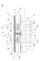
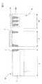
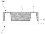
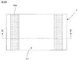
図1は本願の一実施の形態の半導体集積回路装置の製造方法の対象デバイスの一例であるMONOS型記憶構造を有するスプリットゲート型フラッシュメモリにおけるメモリセルアレーの部分上面図である。図2は図1のA−A’断面に対応するデバイス模式断面図である。図3は図2に示すONO膜周辺部R1の部分拡大断面図である。図4は図1に示すスプリットゲート型フラッシュメモリにおけるメモリセルアレーの回路構成図である。図5は図1に示すスプリットゲート型フラッシュメモリの選択セルの書込み、消去および読出し時において、各配線(選択ゲート線、メモリゲート線、ソース線およびビット線)に印加される電圧条件の一例である。 FIG. 1 is a partial top view of a memory cell array in a split gate type flash memory having a MONOS type memory structure, which is an example of a target device of a manufacturing method of a semiconductor integrated circuit device according to an embodiment of the present application. FIG. 2 is a device schematic cross-sectional view corresponding to the cross section A-A ′ of FIG. 1. FIG. 3 is a partially enlarged cross-sectional view of the ONO film peripheral portion R1 shown in FIG. FIG. 4 is a circuit configuration diagram of a memory cell array in the split gate type flash memory shown in FIG. FIG. 5 shows an example of voltage conditions applied to each wiring (selection gate line, memory gate line, source line and bit line) at the time of writing, erasing and reading of the selected cell of the split gate type flash memory shown in FIG. is there.
まず、本願の一実施の形態の半導体集積回路装置の製造方法の対象デバイスであるスプリットゲート型MONOSメモリセルの構造の一例を図1から図3を用いて説明する。これらに基づいて、本願の一実施の形態の半導体集積回路装置の製造方法における対象デバイスの一例であるMONOS構造またはSONOS構造を用いたスプリットゲートフラッシュメモリのメモリセル構造、メモリセルアレーの基本構造、および基本動作を説明する。 First, an example of the structure of a split gate type MONOS memory cell, which is a target device of a method for manufacturing a semiconductor integrated circuit device according to an embodiment of the present application, will be described with reference to FIGS. Based on these, a memory cell structure of a split gate flash memory using a MONOS structure or a SONOS structure, which is an example of a target device in the method for manufacturing a semiconductor integrated circuit device of one embodiment of the present application, a basic structure of a memory cell array, The basic operation will be described.
先ずメモリセル部3(メモリセルアレー)の構造を説明する。このメモリセル部3は、メモリセル繰り返し単位領域3uを単位胞または単位格子とする2次元繰り返し構造を有する。図1から図3に示すように、半導体基板1は、例えばp型の単結晶シリコンからなり、この基板部より高濃度のp型の不純物が導入されてなるpウエル11が形成されている。半導体基板1の第1の主面1a(デバイス形成面すなわち裏面1bの反対の面)の活性領域には、メモリセルの選択用nチャネルMISFET(QS)とメモリ用nチャネルMISFET(QM)とが配置されている。このメモリセルのドレイン領域9およびソース領域8a,8bは、例えば相対的に低濃度のn−型の半導体領域14d,14s(それぞれN型ドレインエクステンション領域、N型ソースエクステンション領域)と、そのn−型の半導体領域14d,14sよりも不純物濃度の高い相対的に高濃度のn+型の半導体領域12(N型高濃度領域)とを有している(LDD(Lightly Doped Drain)構造)。n−型の半導体領域14d,14sは、メモリセルのチャネル領域側に配置され、n+型の半導体領域12は、メモリセルのチャネル領域側からn−型の半導体領域14d,14s分だけ離れた位置に配置されている。n+型の半導体領域12上には、ニッケルシリサイド層等の(ソース・ドレイン上の)シリサイド層15aが設けられている。First, the structure of the memory cell unit 3 (memory cell array) will be described. The
このドレイン領域9とソース領域8a,8bとの間の半導体基板1の主面1a上には、上記選択用nチャネルMISFET(QS)すなわち選択トランジスタの選択ゲート電極6a,6bと、上記メモリ用nチャネルMIS(QM)すなわちメモリトランジスタのメモリゲート電極7a,7bとが隣接して延在しており、その延在方向において複数のメモリセルは半導体基板1に形成された素子分離部5a,5b,5c,5d,5e,5f(STI領域)を介して隣接している。すなわち、マトリクス状のSTI領域群の各列を所定の間隔を置いて、一対のワード線6a,6bが縦断している。 On the
ソース・ドレイン領域上と同様に、メモリゲート電極7a,7b上には、先と同様にニッケルシリサイド層等のシリサイド層15bが設けられている。また、選択ゲート電極6a,6b上には、キャップ絶縁膜19が設けられている。更に、メモリゲート電極7a,7bの外側および選択ゲート電極6a,6bの内側には、サイドウォールスペーサ18が設けられている。 Similar to the source / drain regions, a
選択ゲート電極6a,6bと半導体基板1の主面との間には、例えば厚さ1〜5nm程度の薄い酸化シリコン膜からなるゲート絶縁膜16が設けられている。ゲート絶縁膜16には、酸化シリコン膜以外にも、酸窒化シリコン膜あるいは、酸化ハフニウム膜、酸化アルミニウム膜(アルミナ)または酸化タンタル膜など、窒化シリコン膜よりも高い誘電率を有する金属酸化膜を使用してもよい。 Between the
メモリゲート電極7a,7bは選択ゲート電極6a,6b及びキャップ絶縁膜19からなる積層膜の側面の片側にサイドウォール状に設けられており、下層の絶縁膜17a(電荷蓄積膜下層絶縁膜)、電荷蓄積層17b(電荷蓄積膜)および上層の絶縁膜17c(電荷蓄積膜上層絶縁膜)を積層した電荷保持用絶縁膜17(ONO膜)により選択ゲート電極6a,6bとメモリゲート電極7a,7bとの絶縁がなされている。 The
電荷蓄積層17bは、その上下を絶縁膜17a,17cに挟まれた状態で設けられており、例えば窒化シリコン膜からなり、その厚さは、例えば5〜20nm程度である。窒化シリコン膜は、その膜中に離散的なトラップ準位を有し、このトラップ準位に電荷を蓄積する機能を有する絶縁膜である。本実施の形態においては、トラップ準位を有する絶縁膜として、窒化シリコン膜9bを形成しているが、窒化シリコン膜に限定されものではなく、例えば酸化アルミニウム膜(アルミナ)、酸化ハフニウム膜または酸化タンタル膜など、窒化シリコン膜よりも高い誘電率を有する高誘電率膜を使用してもよい。また、シリコンナノドットで形成してもよい。絶縁膜17a,17cは、例えば酸化シリコン膜等からなり、下層の絶縁膜17aの厚さは、例えば1.5〜6nm程度、上層の絶縁膜17cの厚さは、例えば1〜8nm程度である。絶縁膜17a,17cは窒素を含んだ酸化シリコン膜で形成することもできる。 The
選択ゲート電極6a,6bおよびメモリゲート電極7a,7bの方には窒化シリコン膜および酸化シリコン膜からなる層間絶縁膜21(プリメタル絶縁膜)が形成されており、この層間絶縁膜21にはドレイン領域9に達するコンタクトホール10が形成されている。ドレイン領域9には、コンタクトホール10に埋め込まれたプラグ22(タングステンプラグ)を介して、第1方向(列方向)に延在するメモリゲート電極7a,7b(または選択ゲート電極6a,6b)に対して交差する方向である第2方向(行方向)に延在する第1層配線23が接続されている。この配線23が、各メモリセルのビット線を構成している。 An interlayer insulating film 21 (premetal insulating film) made of a silicon nitride film and a silicon oxide film is formed on the
図1に示すような平面構造のため、STI領域5、5b,5d等のパターニングにおいて、近接効果等のために横長の長方形形状が、その端部24a,24bにおいて、歪むことによって、近接して設けられるMISFET(QS,QM)のゲート幅が変化したり、端部24a,24b間のソース領域8の幅が変化する当の懸念がある。このため、セクション3および5においては、この問題をプロセス的改良によって、克服している。 Due to the planar structure as shown in FIG. 1, in the patterning of the
次に、図4を用いて、スプリットゲート型MONOSメモリセルのアレー構成の一例を説明する。なお、図4では、簡略化のため、2×4個のメモリセルのみを示している。 Next, an example of the array configuration of the split gate type MONOS memory cell will be described with reference to FIG. In FIG. 4, only 2 × 4 memory cells are shown for simplification.
各メモリセルの選択ゲート電極6を接続する選択ゲート線(ワード線)CGL0〜CGL3、メモリゲート電極7を接続するメモリゲート線MGL0〜MGL3および2つの隣接したメモリセルが共有するソース領域8を接続するソース線SL0,SL1は第1の方向(列方向)にそれぞれ平行に延在する。また、メモリセルのドレイン領域9を接続するビット線BL0,BL1は第2の方向(行方向)、すなわち、選択ゲート線CGL0等と直交する方向に延在する。なお、これらの配線は、原則として、回路図上だけでなく、各メモリセルまたは配線のレイアウト上も前述した方向に延在する。また、選択ゲート線CGL0等は、選択ゲート電極6により構成しても良く、選択ゲート電極6に接続される配線により構成してもよい。 Select gate lines (word lines) CGL0 to CGL3 connecting the
ソース線SL0,SL1とメモリゲート線MGL0〜MGL3には、書込み・消去時に高電圧が印加されるので、高耐圧のMISFETからなる昇圧ドライバが接続されている。また、選択ゲート線CGL0〜CGL3には、1.5V程度の低電圧のみが印加されるので、低耐圧で高速の昇圧ドライバが接続されている。1本のローカルビット線には16個、32個または64個のメモリセルが接続され、ローカルビット線はローカルビット線を選択するMISFETを介してグローバルビット線に接続され、グローバルビット線はセンスアンプに接続されている。 Since a high voltage is applied to the source lines SL0 and SL1 and the memory gate lines MGL0 to MGL3 at the time of writing / erasing, a boosting driver made of a high breakdown voltage MISFET is connected. In addition, since only a low voltage of about 1.5 V is applied to the select gate lines CGL0 to CGL3, a low-breakdown-voltage and high-speed boost driver is connected. 16, 32, or 64 memory cells are connected to one local bit line, the local bit line is connected to the global bit line via a MISFET that selects the local bit line, and the global bit line is a sense amplifier. It is connected to the.
図4に示したアレー構成では、ソース線SL0,SL1は一本毎に独立して配線され、メモリゲート線MGL0〜MGL3は複数本を接続して共通のメモリゲート線MGLとしてあるが、ソース線SL0,SL1およびメモリゲート線MGL0〜MGL3ともに複数本を接続して、それぞれ共有のソース線およびメモリゲート線としても良い。共有の配線とすることで、それぞれの線を駆動する高耐圧のドライバ数が削減され、チップ面積を低減することができる。逆に、ソース線SL0,SL1およびメモリゲート線MGL0〜MGL3ともに一本毎に独立して配線しても良い。この場合、高耐圧のドライバ数は多くなるが、書込みおよび消去時にディスターブを受ける時間を減らすことができる。 In the array configuration shown in FIG. 4, source lines SL0 and SL1 are wired independently for each line, and a plurality of memory gate lines MGL0 to MGL3 are connected to form a common memory gate line MGL. A plurality of SL0, SL1 and memory gate lines MGL0 to MGL3 may be connected to form a common source line and memory gate line, respectively. By using the shared wiring, the number of high breakdown voltage drivers for driving each line can be reduced, and the chip area can be reduced. Conversely, the source lines SL0 and SL1 and the memory gate lines MGL0 to MGL3 may be wired independently for each line. In this case, the number of high breakdown voltage drivers increases, but the time for receiving disturbance during writing and erasing can be reduced.
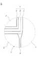
次に、スプリットゲート型MONOSメモリセルのメモリ動作(書込み、消去および読み出し)の一例を図5を用いて説明する。ここでは、電荷蓄積層17bへの電子の注入を「書込み」、ホールの注入を「消去」と定義する。 Next, an example of the memory operation (writing, erasing and reading) of the split gate type MONOS memory cell will be described with reference to FIG. Here, the injection of electrons into the
「書込み」について説明する。 “Write” will be described.
書込みは、いわゆるSSI方式によって行なわれる。図5に示すように、選択セルBIT1のソース領域8に印加する電圧Vsを5V、メモリゲート電極7に印加する電圧Vmgを10V、選択ゲート電極6に印加する電圧Vsgを1Vとする。そして、ドレイン領域9に印加する電圧Vdは書込み時のチャネル電流がある設定値となるように制御する。このときの電圧Vdはチャネル電流の設定値と選択用MISFET(QS)のしきい値電圧によって決まり、例えば設定電流値1μAで0.4V程度となる。pウエル11に印加する電圧Vwellは0Vである。 Writing is performed by the so-called SSI method. As shown in FIG. 5, the voltage Vs applied to the
次に、選択セルBIT1に書込み電圧を印加したときの電荷の動きを説明する。ドレイン領域9よりも大きな電圧を選択ゲート電極6に印加して選択用MISFET(QS)をオン状態とし、ソース領域8に正の高電圧を印加することで、ドレイン領域9からソース領域8へ電子が流れる。チャネル領域を流れるこの電子は、選択ゲート電極6とメモリゲート電極7との境界付近下のチャネル領域(ソース領域8とドレイン領域9との間)で加速されてホットエレクトロンになる。そして、ホットエレクトロンは、メモリゲート電極7に印加された正電圧によってメモリゲート電極7に引き寄せられメモリゲート電極7下の電荷蓄積層17b中に注入される。注入されたホットエレクトロンは、電荷蓄積層17b中のトラップ準位に捕獲され、その結果、電荷蓄積層17bに電子が蓄積されてメモリ用nチャネルMISFET(QM)のしきい値電圧が上昇する。
次に、「消去」について説明する。Next, the movement of charge when a write voltage is applied to the selected cell BIT1 will be described. By applying a voltage higher than that of the
Next, “erase” will be described.
図5の「消去」欄に示すように、消去は、BTBT(Band-To-Band Tunneling)現象によりホールを発生させ電界加速することでホットホールを電荷蓄積層17b中に注入するBTBT消去、メモリゲート電極7または半導体基板1からホールをFN(Fowler-Nordheim)トンネリングで電荷蓄積層中に注入するFN消去のいずれかによって行う。 As shown in the “erase” column of FIG. 5, erasure is performed by BTBT erasure in which hot holes are injected into the
BTBT消去を行う場合は、メモリゲート電極7に印加する電圧Vmgを−6V、ソース領域8に印加する電圧Vsを6V、選択ゲート電極6に印加する電圧Vsgを0Vとし、ドレイン領域9は浮遊状態する。pウエル11には0V(Vwell)を印加する。上記電圧を印加した場合、ソース領域8とメモリゲート電極7との間にかかる電圧によってソース領域8の端部においてBTBT現象で生成されたホールが、ソース領域8に印加された高電圧によって加速されてホットホールとなり、メモリゲート電極7に印加された高電圧によってホットホールがメモリゲート電極7方向へと引っ張られ、電荷蓄積層17b中に注入される。注入されたホットホールは電荷蓄積層17b中のトラップ準位に捕獲され、メモリ用nチャネルMISFET(QM)のしきい値電圧が低下する。 When performing BTBT erase, the voltage Vmg applied to the
メモリゲート電極7からホールを注入するFN消去の場合、ホールのFNトンネル注入が起こりやすいように、図3で上層の絶縁膜17cの厚さを3nm以下とするか、上層の絶縁膜17cがない構造とする。上層の絶縁膜17cがある構造の場合、よりホールが注入しやすいように、上層の絶縁膜17cの間に厚さ1nm程度の窒化シリコン膜またはアモルファスシリコン膜を挿入した構造にすると良い。また、上層の絶縁膜17cがない構造の場合、よりホールが注入しやすいように、電荷蓄積層17bを酸窒化シリコン膜を用いた構造、または窒化シリコン膜および酸窒化シリコン膜を半導体基板側から順に積層した構造とすると良い。メモリゲート電極7からホール注入するFN消去の印加電圧としては、メモリゲート電極7に印加する電圧Vmgを15Vとし、その他ソース領域8に印加する電圧Vs、選択ゲート電極6に印加する電圧Vsg、ドレイン領域9に印加する電圧Vd、pウエル11に印加する電圧Vwellは0Vとする。上記電圧を印加すると、メモリゲート電極7からホールがFNトンネリングで電荷蓄積層17bに注入される。加えて、書き込み時に電荷蓄積層17bに蓄積された電子がメモリゲート電極7へ引き抜かれる。 In the case of FN erasure in which holes are injected from the
半導体基板1からホールを注入するFN消去の場合、ホールのFNトンネル注入が起こりやすいように、図3に示したメモリセルにおいて、下層の絶縁膜17aを3nm以下の膜厚にするか、よりホールを注入しやすいように下層の絶縁膜17aの間に厚さ1nm程度の窒化シリコン膜またはアモルファスシリコン膜を挿入した構造とする。半導体基板1からホール注入するFN消去の印加電圧としては、メモリゲート電極7に印加する電圧Vmgを−15Vとし、その他ソース領域8に印加する電圧Vs、選択ゲート電極6に印加する電圧Vsg、ドレイン領域9に印加する電圧Vd、pウエル11に印加する電圧Vwellは0Vとする。上記電圧を印加すると、半導体基板1からホールがトンネリングで電荷蓄積層17bに注入される。加えて、書き込み時に電荷蓄積層17bに蓄積された電子が半導体基板1へ引き抜かれる。 In the case of FN erasure in which holes are injected from the
次に、「読出し」について説明する。 Next, “reading” will be described.
図5の「読出し」欄に示すように、読出しには、書込みと逆方向に電流を流して読み出す方法と同方向に電流を流して読み出す方法の2種類がある。図5に示すように、書込みと逆方向に電流を流して読み出す場合、ドレイン領域9に印加する電圧Vdを1.5V、ソース領域8に印加する電圧Vsを0V、選択ゲート電極6に印加する電圧Vsgを1.5V、メモリゲート電極7に印加する電圧Vmgを1.5Vとする。書込みと同方向に電流を流して読み出す場合、ドレイン領域9に印加する電圧Vdとソース領域8に印加する電圧Vsを入れ替え、それぞれ0V、1.5Vとする。 As shown in the “Read” column of FIG. 5, there are two types of reading: a method of reading by flowing a current in the opposite direction to the writing and a method of reading by flowing a current in the same direction. As shown in FIG. 5, when reading by reading a current in the opposite direction to writing, the voltage Vd applied to the
読出し時のメモリゲート電極7に印加する電圧Vmgは、書込み状態におけるメモリ用nチャネルMIS(QM)のしきい値電圧と消去状態におけるメモリ用nチャネルMISFET(QM)のしきい値電圧との間に設定する。書込み状態および消去状態のしきい値電圧をそれぞれ4Vおよび−1Vに設定すると、上記読出し時のVmgは両者の中間値となる。中間値とすることで、データ保持中に書込み状態のしきい値電圧が2V低下しても、消去状態のしきい値電圧が2V上昇しても、書込み状態と消去状態を判別することができ、データ保持特性のマージンが広がる。消去状態におけるメモリセルのしきい値電圧を十分低くしておけば、読出し時の電圧Vmgを0Vとすることもできる。読出し時の電圧Vmgを0Vとすることで、読出しディスターブ、すなわち、メモリゲート電極MGへの電圧印加によるしきい値電圧の変動を避けることが可能となる。 The voltage Vmg applied to the
2.本願の一実施の形態の半導体集積回路装置の製造方法におけるウエハプロセスのアウトライン等の説明(主に図6から図29)
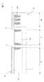
図6は図1に示すスプリットゲート型フラッシュメモリのメモリセル部、周辺回路部、位置合わせ用のターゲットパターンおよびチップ領域の間の相互の位置関係を例示したウエハの部分上面図である。図7は図6のB−B’断面(メモリセルアレー部分は、更に図1のA−A’’断面に対応、以下図29まで同じ)に対応するデバイス断面プロセスフロー図(STI領域加工用窒化シリコン膜成膜工程)である。図8は図6のB−B’断面に対応するデバイス断面プロセスフロー図(STI領域加工用レジスト膜塗布工程)である。図9は図6のB−B’断面に対応するデバイス断面プロセスフロー図(STI領域加工用レジスト膜パターニング工程)である。図10は図6のB−B’断面に対応するデバイス断面プロセスフロー図(STI領域埋め込み&平坦化工程)である。図11は図6のB−B’断面に対応するデバイス断面プロセスフロー図(P型ウエル導入工程)である。図12は図6のB−B’断面に対応するデバイス断面プロセスフロー図(N型ウエル導入工程)である。図13は図6のB−B’断面に対応するデバイス断面プロセスフロー図(ゲート酸化および第1層ポリシリコン層成膜工程)である。図14は図6のB−B’断面に対応するデバイス断面プロセスフロー図(キャップ絶縁膜成膜工程)である。図15は図6のB−B’断面に対応するデバイス断面プロセスフロー図(メモリセル部のゲート電極加工用レジスト塗布工程)である。図16は図6のB−B’断面に対応するデバイス断面プロセスフロー図(メモリセル部のゲート電極加工工程)である。図17は図6のB−B’断面に対応するデバイス断面プロセスフロー図(周辺回路部のキャップ絶縁膜除去工程)である。図18は図6のB−B’断面に対応するデバイス断面プロセスフロー図(ONO膜&第2層ポリシリコン層成膜工程)である。図19は図6のB−B’断面に対応するデバイス断面プロセスフロー図(第2層ポリシリコン層の自己整合エッチング工程)である。図20は図6のB−B’断面に対応するデバイス断面プロセスフロー図(ONO膜&内側ゲート電極加工用レジスト膜パターニング工程)である。図21は図6のB−B’断面に対応するデバイス断面プロセスフロー図(ONO膜&内側ゲート電極エッチング工程)である。図22は図6のB−B’断面に対応するデバイス断面プロセスフロー図(周辺回路部のゲート電極加工用レジスト膜塗布工程)である。図23は図6のB−B’断面に対応するデバイス断面プロセスフロー図(周辺回路部のゲート電極加工工程)である。図24は図6のB−B’断面に対応するデバイス断面プロセスフロー図(サイドウォールスペーサ形成&ソース・ドレイン領域導入工程)である。図25は図6のB−B’断面に対応するデバイス断面プロセスフロー図(シリサイド化工程)である。図26は図6のB−B’断面に対応するデバイス断面プロセスフロー図(コンタクト上窒化シリコン膜成膜工程)である。図27は図6のB−B’断面に対応するデバイス断面プロセスフロー図(プリメタル絶縁膜成膜工程)である。図28は図6のB−B’断面に対応するデバイス断面プロセスフロー図(タングステンプラグ形成工程)である。図29は図6のB−B’断面に対応するデバイス断面プロセスフロー図(第1層メタル配線形成工程)である。これらに基づいて、本願の一実施の形態の半導体集積回路装置の製造方法におけるウエハプロセスのアウトラインを説明する。2. Description of outline of wafer process in manufacturing method of semiconductor integrated circuit device according to one embodiment of the present application (mainly FIGS. 6 to 29)
6 is a partial top view of the wafer illustrating the mutual positional relationship among the memory cell portion, peripheral circuit portion, alignment target pattern and chip region of the split gate flash memory shown in FIG. 7 is a device cross-sectional process flow diagram corresponding to the BB ′ cross section of FIG. 6 (the memory cell array portion further corresponds to the AA ″ cross section of FIG. Silicon nitride film forming step). FIG. 8 is a device cross-sectional process flow diagram (STI region processing resist film coating step) corresponding to the BB ′ cross-section of FIG. 6. FIG. 9 is a device cross-sectional process flow diagram (STI region processing resist film patterning step) corresponding to the BB ′ cross-section of FIG. 6. FIG. 10 is a device cross-sectional process flow diagram (STI region embedding and planarization step) corresponding to the BB ′ cross-section of FIG. FIG. 11 is a device cross-sectional process flow diagram (P-type well introduction step) corresponding to the BB ′ cross-section of FIG. 6. FIG. 12 is a device cross-sectional process flow diagram (N-type well introduction step) corresponding to the BB ′ cross-section of FIG. FIG. 13 is a device cross-sectional process flow diagram (gate oxidation and first polysilicon layer forming step) corresponding to the BB ′ cross-section of FIG. 6. FIG. 14 is a device cross-sectional process flow diagram (cap insulating film forming step) corresponding to the BB ′ cross-section of FIG. 6. FIG. 15 is a device cross-sectional process flow diagram corresponding to the BB ′ cross-section of FIG. FIG. 16 is a device cross-sectional process flow diagram corresponding to the BB ′ cross-section of FIG. 6 (gate electrode processing step of the memory cell portion). FIG. 17 is a device cross-sectional process flow diagram corresponding to the BB ′ cross-section of FIG. 6 (peripheral circuit portion cap insulating film removing step). FIG. 18 is a device cross-sectional process flow diagram (ONO film & second polysilicon layer forming step) corresponding to the BB ′ cross section of FIG. 6. FIG. 19 is a device cross-sectional process flow diagram (second-layer polysilicon layer self-aligned etching step) corresponding to the BB ′ cross-section of FIG. 6. FIG. 20 is a device cross-sectional process flow diagram (ONO film & resist film patterning process for inner gate electrode processing) corresponding to the BB ′ cross section of FIG. 6. 21 is a device cross-sectional process flow diagram (ONO film & inner gate electrode etching step) corresponding to the BB ′ cross-section of FIG. FIG. 22 is a device cross-sectional process flow diagram corresponding to the BB ′ cross-section of FIG. FIG. 23 is a device cross-section process flow diagram (peripheral circuit portion gate electrode processing step) corresponding to the BB ′ cross-section of FIG. 6. FIG. 24 is a device cross-sectional process flow diagram (side wall spacer formation & source / drain region introduction step) corresponding to the BB ′ cross section of FIG. 6. FIG. 25 is a device cross-sectional process flow diagram (silicidation process) corresponding to the BB ′ cross-section of FIG. 6. FIG. 26 is a device cross-sectional process flow diagram (silicon nitride film forming step on contact) corresponding to the BB ′ cross-section of FIG. 6. FIG. 27 is a device cross-sectional process flow diagram (premetal insulating film forming step) corresponding to the BB ′ cross-section of FIG. 6. FIG. 28 is a device cross-sectional process flow diagram (tungsten plug forming step) corresponding to the BB ′ cross-section of FIG. 6. FIG. 29 is a device cross-sectional process flow diagram (first-layer metal wiring forming step) corresponding to the BB ′ cross-section of FIG. 6. Based on these, the outline of the wafer process in the method of manufacturing a semiconductor integrated circuit device according to the embodiment of the present application will be described.
先ず、図6により対象デバイス等のウエハ1上でのレイアウトを説明する。図6に示すように、メモリセル部3(メモリセルアレー)は、チップ領域2の一部を占めており、チップ領域2は、実際の製品回路が形成される製品回路領域である。メモリセル部3の近傍には、通常、CMOSまたはCMIS構成のメモリ周辺回路4が設けられている。チップ領域2の外のスクライブ領域64には、位置合わせ用ターゲットパターン25が置かれている。この位置合わせ用ターゲットパターン25は、X方向位置合わせ用ターゲットパターン25x、Y方向位置合わせ用ターゲットパターン25y等から構成されている。次に、この図6のB−B’断面(メモリセルアレー部については、更に図1のA−A’’断面に対応する)に対応するデバイス断面を使って、ウエハプロセスの概要を説明する。なお、以下で示す断面は、図示の関係上、メモリセル部3、メモリ周辺回路4、X方向位置合わせ用ターゲットパターン25x等の各一部である。メモリ周辺回路4については、CMOSまたはCMIS構成のPチャネル部分の一部を示した。 First, the layout of the target device on the
図7に示すように、各断面は、左からメモリセルアレー3、周辺回路部4、位置合わせ用ターゲットパターン部25にそれぞれ対応する。スターティングマテリアルとして、ウエハ1を準備する。ウエハ1としては、たとえば、P型単結晶シリコンウエハ(シリコン系単結晶ウエハ)等を例示することができる。なお、エピタキシャルウエハでも、SOIウエハでもよい。ウエハ1の寸法としては、たとえば、300φ(直径が300mm程度のほぼ円形)ウエハを例示することができる。ただし、そのほかに200φ、450φ等を例示することができる。以下工程を説明する。 As shown in FIG. 7, each cross section corresponds to the
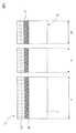
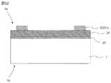
図7に示すように、まず、ウエハ1の第1の主面1a(裏面1bの反対の面)のほぼ全面に、たとえば厚さ10nm程度の熱酸化シリコン膜26(パッド酸化シリコン膜)を形成する。ここで、熱酸化処理としては、たとえば減圧した水素および酸素ガス混合雰囲気中における枚葉ランプ(Lamp)加熱方式(バッチ処理でもよい)等を適用してもよい(以後、「水素酸素ガス混合雰囲気減圧酸化」という)。パッド酸化シリコン膜26は、STI領域を加工するときに、ウエハ1をエッチングダメージから保護するために形成されている。続いて、パッド酸化シリコン膜26上のほぼ全面に、たとえば厚さ90nm程度のSTI領域加工用窒化シリコン膜27をCVD(Chemical Vapor Deposition)法等により、成膜する。 As shown in FIG. 7, first, a thermal silicon oxide film 26 (pad silicon oxide film) having a thickness of, for example, about 10 nm is formed on almost the entire first
次に、図8に示すように、窒化シリコン膜27上のほぼ全面に、STI領域加工用レジスト膜28を塗布する。続いて、このSTI領域加工用レジスト膜28が塗布されたウエハ1をセクション3または4のリソグラフィ処理等により、処理する。ここでは、一例として、セクション3に対応してSTI領域形成工程の概要のみを説明する(詳細はセクション3参照)。 Next, as shown in FIG. 8, an STI region processing resist
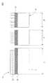
すなわち、セクション3に示す方法により、レジスト膜28を現像すると図9のようになる。続いて、パターニングされたレジスト膜28が存在する状態で、異方性ドライエッチングを実行することにより、シリコン膜27、パッド酸化シリコン膜26およびウエハ1の第1の主面1a(シリコン部材表面領域)をエッチングして、素子分離溝を形成する。その後、レジスト膜28を除去する。更に、ウエハ1の第1の主面側1a表面および素子分離溝内に、たとえばCVD法等により埋め込み絶縁膜5を成膜する。 That is, when the resist
続いて、ウエハ1の第1の主面側1a表面をCMP(Chemical Mechanical Polishing)法等により、平坦化すると、図10のようになる。これで、STI領域5(マトリクス状のSTI領域群)及びターゲットパターン25が完成する。図10には説明簡略化のため、X方向位置合わせ用ターゲットパターン25xを例示しているが、STI領域5(マトリクス状のSTI領域群)及びターゲットパターン25tと同時に、Y方向位置合わせ用ターゲットパターン25yも形成されている。 次に、図11に示すように、メモリセル部3以外の部分をPウエル導入用レジスト膜29で被覆した状態で、イオン打ち込みにより、メモリセル部3にPウエル11を形成する。 Subsequently, when the surface of the first
次に、図12に示すように、周辺回路部4以外の部分をNウエル導入用レジスト膜31で被覆した状態で、イオン打ち込みにより、Nウエル32を形成する。その後、レジスト膜31を除去する。 Next, as shown in FIG. 12, an N well 32 is formed by ion implantation in a state where a portion other than the
次に、図13に示すように、ウエハ1の第1の主面1a表面に、たとえば水素酸素ガス混合雰囲気減圧酸化により、たとえば厚さ7nm程度のゲート絶縁膜16を形成する。更に、その上に、たとえばCVD法等により、たとえば厚さ140nm程度の第1層ポリシリコン膜33を成膜する。 Next, as shown in FIG. 13, a
次に、図14に示すように、第1層ポリシリコン膜33上に、たとえばCVD法等により、たとえば下層のキャップ酸化シリコン膜19a(たとえば厚さ10nm程度)および上層のキャップ窒化シリコン膜19b(たとえば厚さ50nm程度)からなるキャップ絶縁膜19を成膜する。 Next, as shown in FIG. 14, the lower cap
次に、図15に示すように、キャップ絶縁膜19上に、選択ゲートパターニング用レジスト膜34を塗布する。続いて、レジスト膜34が塗布されたウエハ1をリソグラフィ装置(露光装置を含む)に導入して、X方向位置合わせ用ターゲットパターン25xを用いて、X方向(行方向)の位置合わせを実行し、同様に、Y方向位置合わせ用ターゲットパターン25yを用いて、Y方向(行方向)の位置合わせを実行して、光学マスクを用いて、メモリセル部3の選択的露光を行う(言い換えれば、セクション3の図30のマスクによって焼き付けられたX方向位置合わせ用ターゲットパターン25xおよびY方向位置合わせ用ターゲットパターン25yを用いてX方向およびY方向の位置合わせを実行する)。これは、選択ゲートをパターニングする際の位置合わせは、マトリクス状のSTI領域群のX方向の位置を基準として実行されることを意味する。このことにより、図1に示すように、たとえばSTI領域5bの端部24aと選択ゲート電極6aとのX方向(行方向)の位置ずれを最小限に抑えることができる。 Next, as shown in FIG. 15, a select gate patterning resist
ここで、たとえばポジ型レジストを使用したとすると、周辺回路部4については、基本的に露光せず、位置合わせ用ターゲットパターン25については、ほぼ全面露光する。このようにした後、レジスト膜34を現像処理する。 Here, for example, if a positive resist is used, the
このパターニングされたレジスト膜34をマスクとして、異方性ドライエッチングを実行すると、図16のようになる。すなわち、選択ゲート電極6aとキャップ絶縁膜19とからなる積層膜、および、選択ゲート6bとキャップ絶縁膜19とからなる積層膜が形成される。その後、レジスト膜34を除去する。 When anisotropic dry etching is performed using the patterned resist
次に、図17に示すように、周辺回路部4の第1層ポリシリコン33上に形成されたキャップ絶縁膜19bを除去する際には、周辺回路部4以外をレジスト膜35で被覆した状態で、ウエハ1の第1の主面側1aに対して、ウエットエッチング(たとえば、熱燐酸系窒化シリコン膜エッチング液および弗酸系酸化シリコン膜エッチング液)を実行することにより、周辺回路部4のキャップ絶縁膜19bを除去する。キャップ絶縁膜19bを除去する工程においては、キャップ絶縁膜19aがエッチングストッパとして用いられる。その後、レジスト膜35を除去する。周辺回路部4に形成されたキャップ絶縁膜19aは、その後の洗浄工程などを経て、除去される。 Next, as shown in FIG. 17, when removing the
次に、図18に示すように、ウエハ1の第1の主面側1aのほぼ全面に、たとえばCVD法等により、ONO(Oxide Nitride Oxide)膜17を成膜する。続いて、ウエハ1の第1の主面側1aのほぼ全面に、たとえばCVD法等により、たとえば厚さ50nm程度の第2層ポリシリコン膜36を成膜する。 Next, as shown in FIG. 18, an ONO (Oxide Nitride Oxide)
次に、図19に示すように、ウエハ1の第1の主面側1aのほぼ全面に対して、異方性ドライエッチングを実行することにより、選択ゲート電極6aとキャップ絶縁膜19とからなる積層膜、および、6bとキャップ絶縁膜19とからなる積層膜の両側に、その一部がメモリゲート電極7a,7bとなるべき第2層ポリシリコン膜36をサイドウォール状に残存させる。 Next, as shown in FIG. 19, anisotropic dry etching is performed on almost the entire surface of the first
次に、図20に示すように、メモリセル部3の一対の選択ゲート電極6a,6bの一部、残すべきメモリゲート電極7a,7b、周辺回路部4、および、位置合わせ用ターゲットパターン部25をレジスト膜37で被覆した状態で、順次、ポリシリコンの等方性ドライエッチングを実行し、露出している第2層ポリシリコン膜36を除去する。その後、レジスト膜37を除去した後、酸化シリコン膜、窒化シリコン膜等のウエットエッチングを実行することで、露出しているONO膜17を除去すると、図21のようになる。これによって、一対のワード線6a,6bに沿って、自己整合的に第1および第2の電極線7a,7bが形成されたことになる。 Next, as shown in FIG. 20, a part of the pair of
次に、図22に示すように、ウエハ1の第1の主面側1aのほぼ全面に、メモリ周辺回路ゲート加工用レジスト膜38を塗布する。続いて、レジスト膜38が塗布されたウエハ1をリソグラフィ装置(露光装置を含む)に導入して、X方向位置合わせ用ターゲットパターン25xおよびY方向位置合わせ用ターゲットパターン25y(言い換えればセクション3の図30の光学マスクによって露光されたターゲットパターン)を用いて、X方向(行方向)およびY方向(列方向)の位置合わせを実行して、光学マスクを用いて、周辺回路部4の選択的露光を行う。たとえばポジ型レジストを使用したとすると、メモリセル部3および位置合わせ用ターゲットパターン25については、基本的に露光しない。このようにした後、レジスト膜38を現像処理する。ここでは、選択ゲート電極6をパターニングする際に用いたX方向位置合わせ用ターゲットパターン25xおよびY方向位置合わせ用ターゲットパターン25yを周辺回路部4に形成される電極6cのパターニング時にも用いる場合について記載した。この場合、周辺回路部4におけるSTI領域5の露光は、図30の光学マスクによって露光されたターゲットパターンを用いることが好ましい。一方、周辺回路部におけるSTI領域5の露光を図31の光学マスクによって露光されたターゲットパターンを用いることも可能である。その場合は、X方向位置合わせ用ターゲットパターン25xおよびY方向位置合わせ用ターゲットパターン25yに加えて、周辺回路部4に形成される電極6cのパターニング時に用いるX方向位置合わせ用ターゲットパターンおよびY方向位置合わせ用ターゲットパターンを図31の光学マスクを用いてさらに形成することが好ましい。 Next, as shown in FIG. 22, a memory peripheral circuit gate processing resist
次に、図23に示すように、パターニングされたレジスト膜38をマスクとして、異方性ドライエッチングを実行して、周辺回路部4のゲート電極6cを形成する。その後、レジスト膜38を除去する。 Next, as shown in FIG. 23, anisotropic dry etching is performed using the patterned resist
次に、図24によってサイドウォールスペーサ18の形成とイオン打ち込みによる各部のソース・ドレイン領域の導入を説明する。図24に示すように、サイドウォールスペーサ18の形成の前に、N型ドレインエクステンション領域14d、N型ソースエクステンション領域14s、P型エクステンション領域41等を順次導入する。その後、ウエハ1の第1の主面側1aのほぼ全面に、たとえばCVD法等により、絶縁膜として酸化シリコン膜を成膜し、その後、異方性ドライエッチングを実行することにより、サイドウォールスペーサ18を形成する。続いて、P型高濃度領域42、N型高濃度領域12等を順次導入する。ここでは、サイドウォールスペーサを形成する絶縁膜として、酸化シリコン膜を用いたが、酸化シリコン膜に限定されず、窒化シリコン膜、あるいは、酸化シリコン膜および窒化シリコン膜との積層膜によって形成することもできる。 Next, the formation of the
次に、図25に示すように、(ソース・ドレイン上の)シリサイド層15aおよび(メモリゲート上の)シリサイド層15bとして、たとえば、ニッケルシリサイド層を形成する。シリサイド層15bとして、ニッケルシリサイド層以外にも、コバルトシリサイド層、チタンシリサイド層、あるいは、プラチナを含むニッケルシリサイド層で構成しても良い。 Next, as shown in FIG. 25, for example, a nickel silicide layer is formed as the
次に、図26に示すように、ウエハ1の第1の主面側1aのほぼ全面に、たとえばCVD法等により、プリメタル絶縁膜21の一部である窒化シリコン膜21a(厚さは、たとえば40nm程度)を成膜する。 Next, as shown in FIG. 26, a
次に、図27に示すように、ウエハ1の第1の主面側1aのほぼ全面に、たとえばCVD法等により、プリメタル絶縁膜21の一部であるオゾンTEOS酸化シリコン系膜21b(厚さは、たとえば170nm程度)およびプラズマTEOS酸化シリコン系膜21c(厚さは、たとえば100nm程度)を順次成膜する。続いて、必要であれば、CMP処理による平坦化を実施する。更に、たとえばプラズマTEOS酸化シリコン系膜を形成してもよい。 Next, as shown in FIG. 27, an ozone TEOS
次に、図28に示すように、コンタクトホールを形成し、そこに、チタン及び窒化チタン等のバリアメタル膜を介して、タングステンプラグ22を埋め込む。 Next, as shown in FIG. 28, a contact hole is formed, and a
次に、図29に示すように、たとえば第1層銅埋め込み配線23(ビットライン)をシングルダマシン法により形成する。その後、必要な数の配線層および層間絶縁膜を積層して、デバイスを完成する。 Next, as shown in FIG. 29, for example, a first layer copper embedded wiring 23 (bit line) is formed by a single damascene method. Thereafter, a necessary number of wiring layers and interlayer insulating films are stacked to complete the device.
3.本願の一実施の形態の半導体集積回路装置の製造方法におけるSTI領域形成プロセス(多重露光プロセス)等の説明(主に図30から図41)
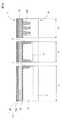
図30は図8から図10のデバイス断面プロセスフロー(STI形成工程)における図1に対応する部分の光学マスク(第1の光学マスク)のパターンの一例を示すマスク平面図である。図31は図8から図10のデバイス断面プロセスフロー(STI形成工程)における図1に対応する部分の光学マスク(第2の光学マスク)のパターンの一例を示すマスク平面図である。図32は図9のデバイス断面プロセスフロー(STI形成工程)における図1に対応する部分のデバイス上面図である。図33は図32のX−X’断面に関するデバイス断面図である。図34は図31の後、レジスト膜を除去した時点の図1に対応する部分のデバイス上面図である。図35は図34のX−X’断面に関するデバイス断面図である。図36は図34の後、ライナ酸化シリコン膜成膜時点の図1に対応する部分のデバイス上面図である。図37は図36の後、酸化シリコン膜で素子分離溝を埋め込んだ時点の図1に対応する部分のデバイス上面図である。図38は図37の後、化学機械研摩により不要な埋め込み酸化シリコン膜を除去した時点の図1に対応する部分のデバイス上面図である。図39は図38の後、窒化シリコン膜除去前の酸化シリコン膜エッチング処理を実行した時点の図1に対応する部分のデバイス上面図である。図40は図39の後、窒化シリコン膜除去処理を実行した時点の図1に対応する部分のデバイス上面図である。図41は図40の後、窒化シリコン膜除去後の酸化シリコン膜エッチング処理(洗浄処理等を含む)を実行した時点の図1に対応する部分のデバイス上面図である。これらに基づいて、本願の一実施の形態の半導体集積回路装置の製造方法におけるSTI領域形成プロセス(多重露光プロセス)を説明する。3. Description of STI region forming process (multiple exposure process) and the like in the method of manufacturing a semiconductor integrated circuit device of one embodiment of the present application (mainly FIGS. 30 to 41)
30 is a plan view of a mask showing an example of the pattern of the optical mask (first optical mask) corresponding to FIG. 1 in the device cross-sectional process flow (STI formation step) of FIGS. 8 to 10. FIG. 31 is a mask plan view showing an example of a pattern of an optical mask (second optical mask) corresponding to FIG. 1 in the device cross-sectional process flow (STI formation step) of FIGS. 8 to 10. 32 is a device top view of a portion corresponding to FIG. 1 in the device cross-section process flow (STI formation step) of FIG. FIG. 33 is a device cross-sectional view regarding the XX ′ cross-section of FIG. 32. FIG. 34 is a device top view of a portion corresponding to FIG. 1 when the resist film is removed after FIG. 35 is a device cross-sectional view with respect to the XX ′ cross-section of FIG. 34. 36 is a device top view of a portion corresponding to FIG. 1 at the time of forming the liner silicon oxide film after FIG. FIG. 37 is a device top view of a portion corresponding to FIG. 1 when the element isolation trench is filled with the silicon oxide film after FIG. FIG. 38 is a device top view of a portion corresponding to FIG. 1 when an unnecessary buried silicon oxide film is removed by chemical mechanical polishing after FIG. FIG. 39 is a device top view of a portion corresponding to FIG. 1 when the silicon oxide film etching process before the silicon nitride film removal is performed after FIG. 40 is a device top view of a portion corresponding to FIG. 1 when the silicon nitride film removing process is executed after FIG. 41 is a device top view of a portion corresponding to FIG. 1 when a silicon oxide film etching process (including a cleaning process and the like) after the removal of the silicon nitride film is performed after FIG. Based on these, the STI region forming process (multiple exposure process) in the method of manufacturing a semiconductor integrated circuit device according to the embodiment of the present application will be described.
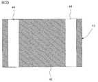
セクション2の図8の状態において、ウエハ1を縮小投影露光装置内に導入して、図30および図31のような第1の光学マスク43および第2の光学マスク46を用いて、STI領域加工用レジスト膜28(ここでは、ネガ型レジスト膜)をたとえば図番の順序でそれぞれ露光する。すなわち、それぞれの露光工程の間に現像する工程を挟まずに、第1の光学マスク43および第2の光学マスク46を用いて、2度続けて露光する。なお、露光の順序は、逆でもよい。第1の光学マスク43には、第1の線状開口群44とそれらを規定するマスクの遮光部45が設けられている。一方、第2の光学マスク46には、第2の線状開口群47とそれらを規定するマスクの遮光部45が設けられている。このレジスト膜28を現像すると、図32のようなパターンとなる。すなわち、レジスト膜28に、行方向が列方向よりも長く、ほぼ矩形形状を有する複数の単位開口48が前記列方向および前記行方向に、マトリクス状に形成される。このように、2枚の光学マスク43、46を用いてそれぞれ露光し、その後の現像により図32のようなレジスト膜28のパターンを作成するため、セクション3で用いるレジスト膜28はネガレジスト膜である必要がある。 In the state of FIG. 8 in
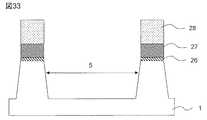
次に、図33に示すように、現像されたレジスト膜28がある状態で、STI領域加工用窒化シリコン膜27、パッド酸化シリコン膜26、ウエハ1の第1の主面1aのシリコン表面領域に対して、異方性ドライエッチング処理を実行すると、STI領域5すなわち、素子分離溝が形成される。このように、直行する2方向において、それぞれの方向に対してマスクを用いて露光を行うことで、矩形形状の端部における近接効果を回避することができ、矩形形状の端部が丸みを帯びるのを回避することができる。これは、本実施の形態においてSTI領域5を形成する際のレジスト膜を角部が存在しない線状のマスクを2枚用い、それぞれのマスクに対して2回の露光を行うことで、矩形形状を有するレジスト膜28を形成しているためである。線状のマスクは、端部や角部を有しないため、近接効果の影響を受けることがないのである。矩形形状の端部が丸みを帯びていると、STI領域5の丸みを帯びている領域上にメモリゲート電極7が形成されてしまい、メモリセルの特性が変動してしまうことが懸念されるが、本実施の形態によると、このようなメモリセルの特性変動を回避することが可能である。さらに、丸みを考慮したマージンを確保する必要もなくなり、メモリセル領域の縮小化を図ることが可能となる。このレジスト膜28を除去すると、図34および図35のようになる。なお、周辺回路部4のSTI領域5のパターニングは、メモリセル部3と同様に行ってもよいが、通常、図30または図31の光学マスクのうち、いずれか一方を用いて実行した方が簡素化される。また、セクション5に説明する方法においては、周辺回路部4のSTI領域5のパターニングは、メモリセル部3と同様に行ってもよいが、通常、図47または図54の光学マスクのうち、いずれか一方を用いて実行した方が簡素化される。更に、セクション5に説明する方法の場合は、他の部分との整合性を考慮すると、図54の光学マスクを用いるのが最も好適である。 Next, as shown in FIG. 33, in the state where the developed resist
次に、図36に示すように、露出した素子分離溝5の内面を熱酸化処理することで、ライナ酸化シリコン膜49を形成する。なお、この熱酸化処理は、前記の水素酸素ガス混合雰囲気減圧酸化でもよい。その場合は、STI領域加工用窒化シリコン膜27の表面も酸化される。 Next, as shown in FIG. 36, a liner
次に、図37に示すように、ウエハ1の第1の主面側1aのほぼ全面を、たとえばHDP(High Density Plasma)を用いたCVD法により、たとえば酸化シリコン膜等の埋め込み絶縁膜5を成膜する。 Next, as shown in FIG. 37, a buried insulating
次に、図38に示すように、ウエハ1の第1の主面側1aに対して、窒化シリコン膜27をストッパとしてCMP処理を実行する。その後、図39に示すように、弗酸系エッチング液を用いて、露出している余剰の埋め込み絶縁膜5をエッチバックする。続いて、図40に示すように、熱燐酸等を用いて、窒化シリコン膜27を除去する。更に、弗酸系エッチング液を用いて、表面の洗浄処理を実行することによって、パッド酸化シリコン膜26および埋め込み絶縁膜5の表層を除去すると図41のようになる。これが、すなわちセクション2の図10の状態である。 Next, as shown in FIG. 38, a CMP process is performed on the first
4.本願の各実施の形態の半導体集積回路装置の製造方法における露光プロセスに使用する位置合わせ用ターゲットパターン等の説明(主に図42から図46)
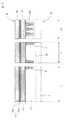
図42は縮小投影露光におけるウエハ、単位露光領域、チップ領域、位置合わせ用ターゲットパターン等の配置を説明するためのウエハ部分上面図(図6は、このチップ及びその周辺領域R2に対応する)である。図43は図42のY方向位置合わせ用ターゲットパターンの拡大上面図である。図44は図42のX方向位置合わせ用ターゲットパターンの拡大上面図である。図45は図44のB−B’断面に対応する位置合わせ用ターゲットパターンの一例の拡大断面図である。図46は図44のB−B’断面に対応する位置合わせ用ターゲットパターンの他の例の拡大断面図である。これらに基づいて、本願の各実施の形態の半導体集積回路装置の製造方法における露光プロセスに使用する位置合わせ用ターゲットパターン等を説明する。4). Description of alignment target pattern used in exposure process in manufacturing method of semiconductor integrated circuit device of each embodiment of the present application (mainly FIGS. 42 to 46)
FIG. 42 is a wafer partial top view for explaining the arrangement of the wafer, unit exposure area, chip area, alignment target pattern and the like in the reduced projection exposure (FIG. 6 corresponds to this chip and its peripheral area R2). is there. 43 is an enlarged top view of the Y-direction alignment target pattern of FIG. FIG. 44 is an enlarged top view of the X-direction alignment target pattern of FIG. 45 is an enlarged cross-sectional view of an example of an alignment target pattern corresponding to the BB ′ cross-section of FIG. FIG. 46 is an enlarged cross-sectional view of another example of the alignment target pattern corresponding to the BB ′ cross-section of FIG. Based on these, the alignment target pattern used in the exposure process in the method of manufacturing a semiconductor integrated circuit device according to each embodiment of the present application will be described.
セクション3で説明したSTI領域のパターニング、ゲート電極のパターニング等で用いるリソグラフィプロセスにおける露光処理、たとえば、縮小投影露光では、通常、図42に示すように、光学マスクを用いたウエハ1に対する露光において、一度に露光できる領域、すなわち、単位露光領域13(ショット領域)には、複数のチップ領域2が含まれる。複数のチップ領域2間のスクライブ領域64には、通常、各パターニング層で形成された位置合わせ用ターゲットパターン25が存在する(一般に、単位パターニング層の同一方向について複数個存在する)。そして、各露光における位置合わせの際には、先行するプロセス層に属する適切なターゲットパターン25を通常、X,Y方向をセットにして使用する。なお、X,Y方向を別々のプロセス層に属するターゲットパターンを用いることもできるが、同一の露光により形成されたターゲットパターンを用いるほうが好ましい。本願では、選択ゲート電極6をパターニングする際に用いるターゲットパターンとして、STI領域の形成の過程で作られたX方向位置合わせ用ターゲットパターン25xおよびY方向位置合わせ用ターゲットパターン25yを使用している。選択ゲート電極6をエッチングする際に用いるレジスト膜を形成するときのX方向位置合わせ用ターゲットパターン25xおよびY方向位置合わせ用ターゲットパターン25yは、レジスト膜28に列方向の線状開口郡44を形成する際の露光により形成することが好ましい。列方向の線状開口郡44により、メモリセルアレーが形成された領域のSTI領域5の行方向の幅が決まり、この幅に対して、選択ゲート電極6の位置を既定することが必要だからである。このようにすることで、選択ゲート電極6の側面にサイドウォール状に形成されるメモリゲート電極7がSTI領域5の端部付近に形成されることを回避できメモリセルの特性を安定させることが可能となる。 In the exposure process in the lithography process used in the patterning of the STI region, the patterning of the gate electrode, etc. described in the
STI領域の形成の過程で作られたターゲットパターン25のY方向位置合わせ用ターゲットパターン25yの全体平面図を図43に示す。位置合わせ用ターゲットパターンの要素パターン25eは、この例では長方形形状(X方向についても同じ)をしているが長方形状には限定されず、他の形状であってもよい。同様に、STI領域の形成の過程で作られたターゲットパターン25のX方向位置合わせ用ターゲットパターン25xの全体平面図を図44に示す。図44のB−B’断面を図22および図15にそれぞれ対応して、図45および図46に示す。ここで、図46では、位置合わせ用ターゲットパターン25の上方に各種の膜が存在するが、半導体基板1と位置合わせ用ターゲットパターンの要素パターン25eの界面の段差によって、光学的な認識が可能である。ただし、図45の方が鮮明に認識することができる。図46でSTI領域の段差が小さく平らに近い状態であるために、ターゲットパターンの上方に各種の膜が形成されたときに光学的な認識が困難な場合がある。その場合には、STI領域が形成された後、すなわち、図10で示された工程の後にマスクを追加して、位置合わせ用ターゲットパターン部25が露出するようなレジスト膜を形成し、STI領域に形成されている埋め込み絶縁膜5をエッチングすることで、ウエハ1とターゲットパターンとの段差を強調する。段差が強調されることで、その後に各種膜が形成されても、強調された段差を反映して形成されるため、光学的に認識することが容易となる。 FIG. 43 shows an overall plan view of the
5.本願の他の実施の形態の半導体集積回路装置の製造方法におけるSTI領域形成プロセス(複合マスク・プロセス)等の説明(主に図47から図57)
このセクションで説明するSTI領域形成プロセスは、セクション3で説明した例の変形例である。このセクションで説明するプロセスは、工程はより複雑になるが、ポジ型レジストを使用できるメリットがある。もちろん、必要があれば、いずれか一方又は両方にネガ型レジストを使用してもよい。5. Description of STI region forming process (composite mask process) in the method of manufacturing a semiconductor integrated circuit device according to another embodiment of the present application (mainly FIGS. 47 to 57)
The STI region formation process described in this section is a modification of the example described in
図47は本願の他の実施形態の半導体装置の製造方法におけるSTI領域形成プロセスを説明するための図1のデバイス部分に対するハードマスク加工用の第1の光学マスクの一例(ポジ型レジストを使用する場合)を示すマスク平面図である。図48は図47の光学マスクを使用して露光、現像したレジスト膜パターン(第1のレジスト膜)の平面図である。図49は図48のX−X’断面に対応するデバイス断面図である。図50は図49に続くデバイス断面図(ハードマスクエッチング完了時点)である。図51は図50に続くデバイス平面図(第1のレジスト膜除去完了時点)である。図52は図51のX−X’断面に対応するデバイス断面図である。図53は図52に続くデバイス断面図(第2のレジスト膜塗布時点)である。図54は本願の他の実施形態の半導体装置の製造方法におけるSTI領域形成プロセスを説明するための図1のデバイス部分に対する第2の光学マスクの一例(ポジ型レジストを使用する場合)を示すマスク平面図である。図55は図53に続き、図54の光学マスクを使用して露光、現像したレジスト膜パターン(第2のレジスト膜)を含むデバイス平面図である。図56は図55のX−X’断面に対応するデバイス断面図である。図57は図55に続くデバイス平面図(第2のレジスト膜除去完了時点)である。これらに基づいて、本願の他の実施の形態の半導体集積回路装置の製造方法におけるSTI領域形成プロセス(複合マスクプロセス)を説明する。 47 is an example of a first optical mask for processing a hard mask (using a positive resist) for the device portion of FIG. 1 for explaining an STI region forming process in a method of manufacturing a semiconductor device according to another embodiment of the present application. FIG. FIG. 48 is a plan view of a resist film pattern (first resist film) exposed and developed using the optical mask of FIG. 49 is a device cross-sectional view corresponding to the X-X ′ cross section of FIG. 48. FIG. 50 is a device cross-sectional view (after completion of hard mask etching) continued from FIG. 49. FIG. 51 is a plan view of the device (at the time when the first resist film removal is completed) following FIG. 52 is a device cross-sectional view corresponding to the X-X ′ cross section of FIG. 51. 53 is a device cross-sectional view (at the time of applying a second resist film) following FIG. FIG. 54 is a mask showing an example (when using a positive resist) of the second optical mask for the device portion of FIG. 1 for explaining the STI region forming process in the method of manufacturing a semiconductor device according to another embodiment of the present application. It is a top view. FIG. 55 is a device plan view including the resist film pattern (second resist film) exposed and developed using the optical mask of FIG. 54, following FIG. 56 is a device cross-sectional view corresponding to the X-X ′ cross section of FIG. 55. FIG. 57 is a device plan view (after completion of the removal of the second resist film) following FIG. Based on these, an STI region forming process (composite mask process) in a method of manufacturing a semiconductor integrated circuit device according to another embodiment of the present application will be described.
セクション2の図7の状態において、STI領域加工用窒化シリコン膜27上に、たとえばCVD法等により、たとえば厚さ30nm程度の酸化シリコン系膜をSTI領域加工用ハードマスク酸化シリコン膜51として成膜する。ハードマスク酸化シリコン膜51は、後のSTI用単位溝領域をエッチングする工程において、エッチングマスクとして用いるものである。したがって、本セクションにおいては、ハードマスク酸化シリコン膜51としているが、それに限定されるものではなく、シリコンからなるウエハに対して高いエッチング選択比を有するものであればよい。続いて、図8と同様に、STI領域加工用ハードマスク酸化シリコン膜51上にSTI領域加工用レジスト膜28を塗布する。続いて、ウエハ1を縮小投影露光装置内に導入して、図47に示すような第1の光学マスク43を用いて、縮小投影露光を実行する。ただし、この例の場合は、図8のSTI領域加工用レジスト膜28は、ポジ型レジストによるSTI領域加工用の第1のレジスト膜28aである。第1の光学マスク43は、第1の線状遮蔽領域群54、それらの間のマスクの開口55等から構成されている。 In the state of FIG. 7 in
露光後、レジスト膜28aを現像すると、図48に示すように、STI領域加工用ハードマスク酸化シリコン膜51上に、線状のSTI領域加工用の第1のレジスト膜28aが残ることと成る。このX−X’断面を、図49に示す。 When the resist
次に、この状態で、図50に示すように、たとえば異方性ドライエッチング等によりSTI領域加工用ハードマスク酸化シリコン膜51をパターニングすることにより、第1の線状膜群52(図51および図52)を形成する。その後、第1のレジスト膜28aを除去すると、図51および図52に示すような状態となる。 Next, in this state, as shown in FIG. 50, the first linear film group 52 (FIG. 51 and FIG. 51) is patterned by patterning the hard mask
次に、図53に示すように、ウエハ1の第1の主面側1aのほぼ全面に、STI領域加工用の第2のレジスト膜28b(たとえば、ポジ型レジスト)を塗布する。次に、図54に示すように、第2の線状遮蔽領域群57、その間のマスクの開口55等からなる第2の光学マスク46を準備する。続いて、第2のレジスト膜28bが塗布されたウエハ1を縮小投影露光装置内に導入して、図54に示すような第2の光学マスク46を用いて、縮小投影露光を実行する。露光後、レジスト膜28bを現像すると、第2の線状膜群53(図55)が得られる。 Next, as shown in FIG. 53, a second resist
次に、相互に直交する第1の線状膜群52および第2の線状膜群53がある状態で、ウエハ1の第1の主面側1aに対して、異方性ドライエッチング等を実行して、STI領域加工用窒化シリコン膜27、パッド酸化シリコン膜26、およびウエハ1の表面1aのシリコン部材をエッチングすると、図55および図56に示すように、素子分離溝5、すなわち、行方向が列方向よりも長く、ほぼ矩形形状を有し、列方向および行方向にマトリクス状を呈するSTI用単位溝領域が形成される。セクション3と同様に、2つの線状のマスクを用いて2回露光し、それにより形成された第1の線状膜群52および第2の線状膜群53を矩形形状のSTI用単位溝領域のエッチングマスクとして用いているため、STI領域5の端部が丸みを帯びることを回避することができる。さらに、本セクションでは、STI用単位溝領域のエッチングマスクの一方に酸化シリコン膜からなる線状膜郡52を用いているため、セクション3で形成するSTI領域5よりも、さらに端部に丸みが帯びないように形成することが可能である。ただし、酸化シリコン膜からなる線状膜郡52を形成するための工程が増加することになる。 Next, with the first
続いて、レジスト膜28bを除去すると、図57のようなウエハ上面の状態となる。この状態は、セクション3における図35に対応する状態であり、その後は、セクション3とほぼ同じ処理を続行すればよい。図57におけるSTI領域加工用ハードマスク酸化シリコン膜51は、後のCMP処理により自動的に除去される。セクション3においては、レジスト膜28に対しての2回の露光の順序は問わなかったが、セクション5においては、ハードマスク酸化シリコン膜51をレジスト膜28bよりも先に形成しておく必要がある。ただし、ハードマスク酸化シリコン膜51は、列方向に用いても行方向に用いてもどちらでも可能である。 Subsequently, when the resist
6.本願の各実施の形態の半導体集積回路装置の製造方法の対象デバイスのその他の一例等の説明(主に図58および図59)
ここで説明するフラッシュメモリは、通常、専用のメモリとして、独立のチップに搭載されるが、組み込み型メモリとすることもできる。ここでは、専用のメモリの場合について具体的に説明する。専用のメモリの場合は、通常、配線系は、たとえば多層のアルミニウム系通常配線23(図59)であるが、ここでは、その第1層配線のみを説明する。このセクションでは、コモングランド(Common Ground)型のNORフラッシュメモリについて、具体的に説明するが、これに限らず、同様のマトリクス上のSTI領域パターンを有するもの等に広く適用できることは言うまでもない。6). Description of other examples of target device of manufacturing method of semiconductor integrated circuit device according to each embodiment of the present application (mainly FIGS. 58 and 59)
The flash memory described here is usually mounted on an independent chip as a dedicated memory, but may be an embedded memory. Here, the case of a dedicated memory will be specifically described. In the case of a dedicated memory, the wiring system is normally a multilayer aluminum-based normal wiring 23 (FIG. 59), but only the first layer wiring will be described here. In this section, a common ground type NOR flash memory will be described in detail. However, the present invention is not limited to this, and it is needless to say that the present invention can be widely applied to those having a similar STI region pattern on a matrix.
このセクションの対象デバイスの製造に関しては、セクション2から5に説明したプロセス等がほぼそのまま、または、以下に説明する対応関係を適用して、実施することができる。 Regarding the manufacture of the target device in this section, the processes and the like described in
図58は本願の各実施形態の半導体装置の製造方法の対象デバイスの他の例を示すNOR型フラッシュメモリの図1に対応するメモリセルアレー部分のデバイス上面図である。図59は図58のA−A’断面に対応するデバイス模式断面図である。これらに基づいて、本願の各実施の形態の半導体集積回路装置の製造方法の対象デバイスのその他の一例を説明する。なお、平面構造及び断面構造とも図1および図2(セクション1)と類似する点が多いので、両者の対応関係および異なる点を中心に説明する。 FIG. 58 is a device top view of the memory cell array portion corresponding to FIG. 1 of the NOR type flash memory showing another example of the target device of the manufacturing method of the semiconductor device of each embodiment of the present application. 59 is a device schematic cross-sectional view corresponding to the A-A ′ cross-section of FIG. 58. Based on these, another example of the target device of the manufacturing method of the semiconductor integrated circuit device of each embodiment of the present application will be described. Since both the planar structure and the cross-sectional structure are similar to those in FIGS. 1 and 2 (section 1), the description will focus on the correspondence and differences between the two.
図58および図59に示すように、STI領域5a,5b,5c,5d,5e,5fの個々の形状および配列はセクション1の例と全く同一である。セクション1の例との最も大きな違いは、コントロールゲート電極6a,6bは、第2層ポリシリコン膜(通常、ポリサイド膜)から構成されているところである。その下には、電極間絶縁膜63(インターポリ絶縁膜)を介して、第1層ポリシリコン膜から構成され、個々のセルに対応して分離されたフローティングゲート62(電荷蓄積ゲート)が設けられている。 As shown in FIGS. 58 and 59, the individual shapes and arrangements of the
ここで、STI領域5a,5b,5c,5d,5e,5fの個々の形状および配列はセクション1の例と全く同一であるので、セクション3および5の各プロセスを適用することができる。その際、コントロールゲート電極6a,6bは、セクション1の選択ゲート電極6a,6bに対応しているものとすればよい。 Here, since the individual shapes and arrangements of the
7.本願の各実施の形態の半導体集積回路装置の製造方法におけるリソグラフィ全体に関する説明
(1)セクション3またはセクション5に説明した露光プロセスは、たとえば、65nmテクノロジノードの製品の場合(90nmテクノロジノードなどのより最小寸法が長い製品を含む)は、バイナリ光学マスク、ArFエキシマレーザ光(波長193nm)および非液浸系縮小露光装置を用いて露光するのが好適である。これを「ArF非液浸露光方式」という。
(2)一方、45nmテクノロジノードおよび32nmテクノロジノードの製品の場合は、(1)の方法または、バイナリ光学マスク、ArFエキシマレーザ光(波長193nm)および液浸系縮小露光装置(水または水よりも高屈折率の高屈折率液体)を用いて露光するのが好適である。後者を「ArF液浸露光方式」という。
(3)更に、22nmテクノロジノード、16nmテクノロジノードおよび10nmテクノロジノードの製品の場合は、バイナリ光学マスクおよび波長15nm程度の軟X線によるEUV(Extreme Ultraviolet)反射縮小投影露光装置を用いて露光するのが好適である。これを「EUV露光方式」という。なお、EUV露光方式では、反射型光学マスクを使用するため、前記実施の形態で示した光学マスクにおいて、以下の変換が必要である。光透過部(開口部)を反射部へ、遮光部を光吸収部(光減衰部)にそれぞれ変換する。
(4)以上のいずれの露光方式を用いた場合にも、STI領域のパターンが2次元周期パターン、すなわち、行列上に周期的に並んだパターンであることから、バイナリ光学マスクに代えて、ハーフトーン型位相シフトマスク、レベンソン型位相シフトマスク、またはその他の形式の位相シフトマスクが適用できる。7). Description of the entire lithography in the method of manufacturing a semiconductor integrated circuit device of each embodiment of the present application (1) The exposure process described in the
(2) On the other hand, in the case of 45 nm technology node and 32 nm technology node products, the method of (1) or binary optical mask, ArF excimer laser light (wavelength 193 nm) and immersion reduced exposure apparatus (more than water or water) It is preferable to perform exposure using a high refractive index liquid having a high refractive index. The latter is called “ArF immersion exposure method”.
(3) Further, in the case of products of the 22 nm technology node, the 16 nm technology node, and the 10 nm technology node, exposure is performed using a binary optical mask and a soft X-ray EUV (Extreme Ultraviolet) reflection reduction projection exposure apparatus. Is preferred. This is called “EUV exposure method”. In the EUV exposure method, since a reflective optical mask is used, the following conversion is necessary in the optical mask shown in the above embodiment. The light transmission part (opening part) is converted into a reflection part, and the light shielding part is converted into a light absorption part (light attenuation part).
(4) When any of the above exposure methods is used, the pattern of the STI region is a two-dimensional periodic pattern, that is, a pattern periodically arranged on a matrix. A tone type phase shift mask, a Levenson type phase shift mask, or other types of phase shift masks can be applied.
8.サマリ
以上本発明者によってなされた発明を実施形態に基づいて具体的に説明したが、本発明はそれに限定されるものではなく、その要旨を逸脱しない範囲において種々変更可能であることは言うまでもない。8). Summary The invention made by the present inventor has been specifically described based on the embodiments. However, the present invention is not limited thereto, and it goes without saying that various changes can be made without departing from the scope of the invention.
例えば、先の実施の形態においては、MONOS構造またはSONOS構造を用いたスプリットゲートフラッシュメモリセルを有するフラッシュメモリを例にとり、具体的に説明したが、本発明はそれに限定されるものではなく、同様な素子分離領域の形状及び配列を有する独立したまたは他のチップに組み込まれたフラッシュメモリ、DRAM(Dynamic Random Access Memory)、SRAM(Static Random Access Memory)およびその他のメモリ等に適用できることは言うまでもない。 For example, in the previous embodiment, the flash memory having the split gate flash memory cell using the MONOS structure or the SONOS structure has been specifically described as an example. However, the present invention is not limited thereto, and Needless to say, the present invention can be applied to flash memories, DRAMs (Dynamic Random Access Memory), SRAMs (Static Random Access Memory), and other memories which have a shape and arrangement of various element isolation regions and are incorporated in other chips.
1 ウエハ又は半導体チップ(半導体基板、p型シリコン単結晶基板)
1a 半導体基板の表面(第1の主面または同主面側)
1b 半導体基板の裏面(第2の主面)
2 半導体チップ又はチップ領域
3 メモリセル部(メモリセルアレー)
3u メモリセル繰り返し単位領域
4 周辺回路部
5、5a,5b,5c,5d,5e,5f STI領域、STI溝領域または素子分離溝(埋め込み絶縁膜)
6,6a,6b 選択ゲート電極またはワード線(コントロールゲート電極)
6c 周辺回路部ゲート電極
7,7a,7b メモリゲート電極(電極線)
8,8a,8b メモリ部ソース領域
9 メモリ部ドレイン領域
10 ビット線コンタクト(またはコンタクトホール)
11 Pウエル
12 N型高濃度領域
13 単位露光領域
14d N型ドレイン・エクステンション領域
14s N型ソース・エクステンション領域
15a (ソース・ドレイン上の)シリサイド層
15b (ゲート上の)シリサイド層
16 ゲート絶縁膜
17 ONO膜
17a 電荷蓄積膜下層絶縁膜
17b 電荷蓄積膜
17c 電荷蓄積膜上層絶縁膜
18 サイドウォールスペーサ
19 キャップ絶縁膜
19a キャップ酸化シリコン膜
19b キャップ窒化シリコン膜
21 プリメタル絶縁膜
21a 窒化シリコン膜
21b オゾンTEOS酸化シリコン系膜
21c プラズマTEOS酸化シリコン系膜
22 タングステンプラグ
23 第1層メタル配線(ビット線)
24 STI領域の端部
25 位置合わせ用ターゲットパターン
25e 位置合わせ用ターゲットパターンの要素パターン
25x X方向位置合わせ用ターゲットパターン
25y Y方向位置合わせ用ターゲットパターン
26 パッド酸化シリコン膜
27 STI領域加工用窒化シリコン膜(窒化シリコン系膜)
28 STI領域加工用レジスト膜
28a STI領域加工用の第1のレジスト膜
28b STI領域加工用の第2のレジスト膜
29 Pウエル導入用レジスト膜
31 Nウエル導入用レジスト膜
32 Nウエル
33 第1層ポリシリコン膜
34 選択ゲートパターニング用レジスト膜
35 周辺回路部ポリシリコン上キャップ除去用レジスト膜
36 第2層ポリシリコン膜
37 内側ゲート除去用レジスト膜
38 メモリ周辺回路ゲート加工用レジスト膜
40 メモリ周辺回路ソース・ドレイン領域
41 P型エクステンション領域
42 P型高濃度領域
43 第1の光学マスク
44 第1の線状開口群
45 マスクの遮光部
46 第2の光学マスク
47 第2の線状開口群
48 レジスト膜の単位開口
49 ライナ酸化シリコン膜
51 STI領域加工用ハードマスク酸化シリコン膜
52 第1の線状膜群
53 第2の線状膜群
54 第1の線状遮蔽領域群
55 マスクの開口
57 第2の線状遮蔽領域群
61 コントロールゲート(ワード線)
62 フローティングゲート
63 電極間絶縁膜(インターポリ絶縁膜)
64 スクライブ領域
BIT1 選択セル
BL0,BL1 ビット線
CGL0,CGL1,CGL2,CGL3 選択ゲート線(ワード線)
MGL,MGL0,MGL1,MGL2,MGL3 メモリゲート線
QM メモリトランジスタ
QS 選択トランジスタ
R1 ONO膜周辺部
R2 チップ及びその周辺領域
SL0,SL1 ソース線1 Wafer or semiconductor chip (semiconductor substrate, p-type silicon single crystal substrate)
1a Semiconductor substrate surface (first main surface or main surface side)
1b Back surface of semiconductor substrate (second main surface)
2 Semiconductor chip or
3u Memory cell repeating
6, 6a, 6b Select gate electrode or word line (control gate electrode)
6c Peripheral circuit
8, 8a, 8b Memory
11 P well 12 N type
24 STI region end 25
28 STI region processing resist
62 Floating
64 Scribe area BIT1 Selected cell BL0, BL1 Bit line CGL0, CGL1, CGL2, CGL3 Select gate line (word line)
MGL, MGL0, MGL1, MGL2, MGL3 Memory gate line QM Memory transistor QS selection transistor R1 ONO film peripheral part R2 Chip and its peripheral area SL0, SL1 Source line
Claims (8)
Translated fromJapanese(a)ウエハの第1の主面上にネガ型レジスト膜を形成する工程;
(b)前記第1の主面のメモリセルアレーとなるべき部分上の前記レジスト膜に、行方向が列方向よりも長く、矩形形状を有する複数の単位開口を前記列方向および前記行方向に、マトリクス状に形成する工程;
(c)前記工程(b)の後、前記レジスト膜がある状態で、前記第1の主面側に対して、エッチング処理を実行することにより、前記第1の主面にSTI用溝領域を形成する工程;
(d)前記STI用溝領域を埋め込むように、埋め込み絶縁膜を前記第1の主面側に形成する工程;
(e)前記STI用溝領域外の前記埋め込み絶縁膜を平坦化処理で除去することにより、マトリクス状のSTI領域群を形成する工程;
(f)前記工程(e)の後、前記マトリクス状のSTI領域群の各列を所定の間隔を置いて縦断する前記メモリセルアレーの第1及び第2のワード線をリソグラフィ処理により形成する工程、
ここで、前記工程(b)は以下の下位工程を含む:
(b1)列方向に延びる第1の線状開口群を有する第1の光学マスクを用いて、前記ネガ型レジスト膜を露光する工程;
(b2)行方向に延びる第2の線状開口群を有する第2の光学マスクを用いて、前記ネガ型レジスト膜を露光する工程;
(b3)前記工程(b1)および(b2)の後、前記ネガ型レジスト膜を現像することにより、前記複数の単位開口を開口する工程、
更に、ここで、前記ウエハ上には、リソグラフィ処理の露光工程における位置合わせに用いる第1ターゲットパターンが形成されるスクライブ領域があり、
前記(a)工程において、前記レジスト膜は前記スクライブ領域にも形成され、
前記工程(b1)における露光で、前記スクライブ領域の前記レジスト膜に対して前記第1ターゲットパターンの露光を行い、
前記工程(c)において、前記スクライブ領域に前記第1ターゲットパターン用溝領域を形成し、
前記工程(d)において、前記第1ターゲットパターン用溝領域中にも前記埋め込み絶縁膜を形成し、
前記工程(e)において、前記第1ターゲットパターン用溝領域外の前記埋め込み絶縁膜を平坦化処理で除去することにより、前記第1ターゲットパターンが形成され、
前記工程(f)の前記リソグラフィ処理中の露光工程における位置合わせは、前記第1ターゲットパターンを用いて行なわれる。A method of manufacturing a semiconductor integrated circuit device including the following steps:
(A) forming a negative resist film on the first main surface of the wafer;
(B) A plurality of unit openings having a row shape in the row direction longer than the column direction and having a rectangular shape are formed in the column direction and the row direction in the resist film on the portion to be the memory cell array on the first main surface. Forming in a matrix;
(C) After the step (b), by performing an etching process on the first main surface side in a state where the resist film is present, an STI trench region is formed on the first main surface. Forming step;
(D) forming a buried insulating film on the first main surface side so as to bury the STI trench region;
(E) forming a matrix-shaped STI region group byremoving the buried insulating film outside the STI trench region by planarization;
(F) After the step (e), a step of forming, by lithography, the first and second word lines of the memory cell array that vertically traverse each column of the matrix-like STI region group at a predetermined interval. ,
Here, the step (b) includes the following substeps:
(B1) exposing the negative resist film using a first optical mask having a first linear aperture group extending in the column direction;
(B2) exposing the negative resist film using a second optical mask having a second linear aperture group extending in the row direction;
(B3) a step of opening the plurality of unit openings by developing the negative resist film after the steps (b1) and (b2);
Furthermore, here, on the wafer, there is a scribe region where a first target pattern used for alignment in an exposure process of lithography processing is formed,
In the step (a), the resist film is also formed in the scribe region,
In the exposure in the step (b1), the first target pattern is exposed to the resist film in the scribe region,
In the step (c), the first target pattern groove region is formed in the scribe region,
In the step (d), the buried insulating film is formed also in the first target pattern trench region,
In the step (e), the first target pattern is formed by removing the buried insulating film outside the trench region for the first target pattern by a planarization process,
The alignment in the exposure step during the lithography process in the step (f) is performed using the first target pattern .
(g)前記工程(a)の前に、前記第1の主面上に窒化シリコン系膜を形成する工程。The method for manufacturing a semiconductor integrated circuit device accordingto claim 1 , further comprising the following steps:
(G ) A step of forming a silicon nitride film on the first main surface before the step (a).
(h)前記工程(f)の後、前記第1及び第2のワード線の各々に沿って、それらの外側にそれらと自己整合的に第1及び第2の電極線を形成する工程。The method for manufacturing a semiconductor integrated circuit device according to claim 1, further comprising the following steps:
(H) After the step (f), a step of forming first and second electrode lines along each of the first and second word lines on the outside thereof in a self-aligning manner with them .
Priority Applications (4)
| Application Number | Priority Date | Filing Date | Title |
|---|---|---|---|
| JP2009273241AJP5554973B2 (en) | 2009-12-01 | 2009-12-01 | Manufacturing method of semiconductor integrated circuit device |
| CN201010570001.1ACN102136447B (en) | 2009-12-01 | 2010-11-30 | Method of manufacturing semiconductor integrated circuit device |
| US12/956,338US8133795B2 (en) | 2009-12-01 | 2010-11-30 | Method of manufacturing semiconductor integrated circuit device |
| US13/365,183US8569144B2 (en) | 2009-12-01 | 2012-02-02 | Method of manufacturing semiconductor integrated circuit device |
Applications Claiming Priority (1)
| Application Number | Priority Date | Filing Date | Title |
|---|---|---|---|
| JP2009273241AJP5554973B2 (en) | 2009-12-01 | 2009-12-01 | Manufacturing method of semiconductor integrated circuit device |
Publications (2)
| Publication Number | Publication Date |
|---|---|
| JP2011119331A JP2011119331A (en) | 2011-06-16 |
| JP5554973B2true JP5554973B2 (en) | 2014-07-23 |
Family
ID=44069214
Family Applications (1)
| Application Number | Title | Priority Date | Filing Date |
|---|---|---|---|
| JP2009273241AExpired - Fee RelatedJP5554973B2 (en) | 2009-12-01 | 2009-12-01 | Manufacturing method of semiconductor integrated circuit device |
Country Status (3)
| Country | Link |
|---|---|
| US (2) | US8133795B2 (en) |
| JP (1) | JP5554973B2 (en) |
| CN (1) | CN102136447B (en) |
Families Citing this family (25)
| Publication number | Priority date | Publication date | Assignee | Title |
|---|---|---|---|---|
| US20120153373A1 (en)* | 2010-12-16 | 2012-06-21 | Nanya Technology Corporation | Gate structure |
| JP5779068B2 (en)* | 2011-10-03 | 2015-09-16 | ルネサスエレクトロニクス株式会社 | Manufacturing method of semiconductor device |
| US8569173B2 (en)* | 2011-12-08 | 2013-10-29 | Globalfoundries Singapore Pte Ltd | Methods of protecting elevated polysilicon structures during etching processes |
| JP5815447B2 (en) | 2012-03-21 | 2015-11-17 | ルネサスエレクトロニクス株式会社 | Manufacturing method of semiconductor device |
| CN103390589B (en)* | 2012-05-09 | 2015-08-26 | 无锡华润上华半导体有限公司 | NOR structure flash memory and preparation method thereof |
| US10403766B2 (en)* | 2012-12-04 | 2019-09-03 | Conversant Intellectual Property Management Inc. | NAND flash memory with vertical cell stack structure and method for manufacturing same |
| US8921947B1 (en)* | 2013-06-10 | 2014-12-30 | United Microelectronics Corp. | Multi-metal gate semiconductor device having triple diameter metal opening |
| US20150017774A1 (en)* | 2013-07-10 | 2015-01-15 | Globalfoundries Inc. | Method of forming fins with recess shapes |
| US8953380B1 (en)* | 2013-12-02 | 2015-02-10 | Cypress Semiconductor Corporation | Systems, methods, and apparatus for memory cells with common source lines |
| US9224842B2 (en) | 2014-04-22 | 2015-12-29 | Globalfoundries Inc. | Patterning multiple, dense features in a semiconductor device using a memorization layer |
| JP6363431B2 (en)* | 2014-08-27 | 2018-07-25 | ルネサスエレクトロニクス株式会社 | Manufacturing method of semiconductor device |
| US9378968B2 (en)* | 2014-09-02 | 2016-06-28 | United Microelectronics Corporation | Method for planarizing semiconductor device |
| JP2017045947A (en)* | 2015-08-28 | 2017-03-02 | ルネサスエレクトロニクス株式会社 | Semiconductor device and manufacturing method for semiconductor device |
| US9711521B2 (en)* | 2015-08-31 | 2017-07-18 | Taiwan Semiconductor Manufacturing Co., Ltd. | Substrate fabrication method to improve RF (radio frequency) device performance |
| US9761546B2 (en) | 2015-10-19 | 2017-09-12 | Taiwan Semiconductor Manufacturing Co., Ltd. | Trap layer substrate stacking technique to improve performance for RF devices |
| US9997253B1 (en)* | 2016-12-08 | 2018-06-12 | Cypress Semiconductor Corporation | Non-volatile memory array with memory gate line and source line scrambling |
| US9842839B1 (en)* | 2017-01-12 | 2017-12-12 | Micron Technology, Inc. | Memory cell, an array of memory cells individually comprising a capacitor and a transistor with the array comprising rows of access lines and columns of digit lines, a 2T-1C memory cell, and methods of forming an array of capacitors and access transistors there-above |
| CN108831829B (en)* | 2018-06-19 | 2020-10-27 | 上海华力微电子有限公司 | A process for sidewall gate isolation etching film under split gate structure |
| KR102446403B1 (en)* | 2018-06-22 | 2022-09-21 | 삼성전자주식회사 | Semiconductor device, method for fabricating the same and layout design method for the same |
| CN110047750B (en)* | 2019-03-28 | 2021-07-27 | 上海华力微电子有限公司 | Method for preventing substrate damage caused by ONO etching |
| US11049807B2 (en) | 2019-09-25 | 2021-06-29 | Sandisk Technologies Llc | Three-dimensional memory device containing tubular blocking dielectric spacers |
| CN110767803B (en)* | 2019-10-15 | 2020-09-18 | 北京元芯碳基集成电路研究院 | Global manufacturing method for source-drain metal of carbon nanotube device |
| US11424257B2 (en)* | 2019-10-15 | 2022-08-23 | Ememory Technology Inc. | Method for manufacturing semiconductor structure and capable of controlling thicknesses of oxide layers |
| JP2021077831A (en)* | 2019-11-13 | 2021-05-20 | ルネサスエレクトロニクス株式会社 | Semiconductor device |
| US12349495B2 (en)* | 2020-02-21 | 2025-07-01 | Canon Kabushiki Kaisha | Semiconductor device and method for manufacturing semiconductor device |
Family Cites Families (22)
| Publication number | Priority date | Publication date | Assignee | Title |
|---|---|---|---|---|
| JPS63232318A (en)* | 1987-03-20 | 1988-09-28 | Hitachi Ltd | Fine pattern formation method |
| JPH05326358A (en)* | 1992-05-18 | 1993-12-10 | Sony Corp | Method for forming fine pattern |
| JPH09289153A (en)* | 1996-04-23 | 1997-11-04 | Oki Electric Ind Co Ltd | Manufacture of semiconductor device and mask used therefor |
| JP3602313B2 (en)* | 1997-06-30 | 2004-12-15 | 富士通株式会社 | Method for manufacturing semiconductor device |
| JP3361973B2 (en)* | 1997-10-13 | 2003-01-07 | 株式会社東芝 | Semiconductor device manufacturing method and semiconductor device |
| JPH11265994A (en)* | 1998-03-17 | 1999-09-28 | Fujitsu Ltd | Method for manufacturing semiconductor device |
| JP2001102440A (en)* | 1999-09-29 | 2001-04-13 | Nec Corp | Manufacturing method of semiconductor integrated circuit |
| JP4823408B2 (en)* | 2000-06-08 | 2011-11-24 | ルネサスエレクトロニクス株式会社 | Nonvolatile semiconductor memory device |
| JP2002208629A (en)* | 2000-11-09 | 2002-07-26 | Toshiba Corp | Semiconductor device and method of manufacturing semiconductor device |
| US6440816B1 (en)* | 2001-01-30 | 2002-08-27 | Agere Systems Guardian Corp. | Alignment mark fabrication process to limit accumulation of errors in level to level overlay |
| CN1379445A (en)* | 2001-04-03 | 2002-11-13 | 华邦电子股份有限公司 | Lithography Process for Reducing the Opening Size of Contact Window |
| US6777168B2 (en)* | 2001-12-14 | 2004-08-17 | Mosel Vitelic, Inc. | Multiple photolithographic exposures with different clear patterns |
| JP2004207564A (en)* | 2002-12-26 | 2004-07-22 | Fujitsu Ltd | Semiconductor device manufacturing method and semiconductor device |
| JP2006041354A (en)* | 2004-07-29 | 2006-02-09 | Renesas Technology Corp | Semiconductor device and manufacturing method thereof |
| JP4758625B2 (en) | 2004-08-09 | 2011-08-31 | ルネサスエレクトロニクス株式会社 | Semiconductor device |
| US7416956B2 (en)* | 2004-11-23 | 2008-08-26 | Sandisk Corporation | Self-aligned trench filling for narrow gap isolation regions |
| KR100684885B1 (en)* | 2005-10-24 | 2007-02-20 | 삼성전자주식회사 | Nonvolatile Memory Device and Manufacturing Method Thereof |
| JP2007128944A (en)* | 2005-11-01 | 2007-05-24 | Sharp Corp | Nonvolatile semiconductor memory device |
| JP4398420B2 (en)* | 2005-11-17 | 2010-01-13 | 株式会社ルネサステクノロジ | Manufacturing method of semiconductor device |
| JP2007214243A (en)* | 2006-02-08 | 2007-08-23 | Renesas Technology Corp | Manufacturing method for semiconductor device |
| JP2008010724A (en)* | 2006-06-30 | 2008-01-17 | Sharp Corp | Semiconductor device and manufacturing method thereof |
| JP2009054707A (en) | 2007-08-24 | 2009-03-12 | Renesas Technology Corp | Semiconductor memory device and manufacturing method thereof |
- 2009
- 2009-12-01JPJP2009273241Apatent/JP5554973B2/ennot_activeExpired - Fee Related
- 2010
- 2010-11-30CNCN201010570001.1Apatent/CN102136447B/ennot_activeExpired - Fee Related
- 2010-11-30USUS12/956,338patent/US8133795B2/ennot_activeExpired - Fee Related
- 2012
- 2012-02-02USUS13/365,183patent/US8569144B2/enactiveActive
Also Published As
| Publication number | Publication date |
|---|---|
| JP2011119331A (en) | 2011-06-16 |
| US8133795B2 (en) | 2012-03-13 |
| US8569144B2 (en) | 2013-10-29 |
| CN102136447A (en) | 2011-07-27 |
| US20110129984A1 (en) | 2011-06-02 |
| CN102136447B (en) | 2015-03-25 |
| US20120129317A1 (en) | 2012-05-24 |
Similar Documents
| Publication | Publication Date | Title |
|---|---|---|
| JP5554973B2 (en) | Manufacturing method of semiconductor integrated circuit device | |
| JP4659527B2 (en) | Manufacturing method of semiconductor device | |
| TWI390710B (en) | Split gate memory cell in fin field effect transistor | |
| US10439032B2 (en) | Semiconductor device and method of manufacturing same | |
| KR20010005584A (en) | Nonvolatile semiconductor storage device and method for manufacturing the same and semiconductor device and method for manufacturing the same | |
| US11222899B2 (en) | Semiconductor device which includes fins and method of making same | |
| JP2018107176A (en) | Semiconductor device manufacturing method and semiconductor device | |
| US10243085B2 (en) | Semiconductor device and method of manufacturing same | |
| US9748360B2 (en) | Manufacturing method of semiconductor device | |
| US7994587B2 (en) | Semiconductor device and semiconductor device manufacturing method | |
| JP2006019570A (en) | Nonvolatile semiconductor storage device and manufacturing method thereof | |
| JP2002208646A (en) | Semiconductor device and method of manufacturing semiconductor device | |
| CN103545261B (en) | Three-dimensional nonvolatile memory cell array with mosaic word lines and method of forming the same | |
| CN101345216A (en) | Method for manufacturing flash memory | |
| JP2005116582A (en) | Semiconductor device and its manufacturing method | |
| TWI812572B (en) | Semiconductor device | |
| US20230328972A1 (en) | Flash memory layout to eliminate floating gate bridge | |
| JP5183711B2 (en) | Manufacturing method of semiconductor device | |
| JP2007134534A (en) | Method of manufacturing semiconductor device | |
| JP4651461B2 (en) | Semiconductor device and manufacturing method thereof | |
| JP2006310687A (en) | Nonvolatile semiconductor memory and manufacturing method thereof | |
| KR20080015616A (en) | Manufacturing method of semiconductor device | |
| JP2007067223A (en) | Semiconductor device and method for manufacturing same | |
| KR20070062816A (en) | Manufacturing Method of Flash Memory Device | |
| KR20070063076A (en) | Manufacturing Method of Semiconductor Device |
Legal Events
| Date | Code | Title | Description |
|---|---|---|---|
| A621 | Written request for application examination | Free format text:JAPANESE INTERMEDIATE CODE: A621 Effective date:20120807 | |
| A977 | Report on retrieval | Free format text:JAPANESE INTERMEDIATE CODE: A971007 Effective date:20131113 | |
| A131 | Notification of reasons for refusal | Free format text:JAPANESE INTERMEDIATE CODE: A131 Effective date:20131121 | |
| A521 | Request for written amendment filed | Free format text:JAPANESE INTERMEDIATE CODE: A523 Effective date:20140115 | |
| TRDD | Decision of grant or rejection written | ||
| A01 | Written decision to grant a patent or to grant a registration (utility model) | Free format text:JAPANESE INTERMEDIATE CODE: A01 Effective date:20140515 | |
| A61 | First payment of annual fees (during grant procedure) | Free format text:JAPANESE INTERMEDIATE CODE: A61 Effective date:20140530 | |
| R150 | Certificate of patent or registration of utility model | Ref document number:5554973 Country of ref document:JP Free format text:JAPANESE INTERMEDIATE CODE: R150 | |
| S531 | Written request for registration of change of domicile | Free format text:JAPANESE INTERMEDIATE CODE: R313531 | |
| R350 | Written notification of registration of transfer | Free format text:JAPANESE INTERMEDIATE CODE: R350 | |
| LAPS | Cancellation because of no payment of annual fees |