JP5554417B2 - Trench gate power semiconductor device and manufacturing method thereof - Google Patents
Trench gate power semiconductor device and manufacturing method thereofDownload PDFInfo
- Publication number
- JP5554417B2 JP5554417B2JP2012540208AJP2012540208AJP5554417B2JP 5554417 B2JP5554417 B2JP 5554417B2JP 2012540208 AJP2012540208 AJP 2012540208AJP 2012540208 AJP2012540208 AJP 2012540208AJP 5554417 B2JP5554417 B2JP 5554417B2
- Authority
- JP
- Japan
- Prior art keywords
- trench gate
- semiconductor device
- power semiconductor
- gate power
- region
- Prior art date
- Legal status (The legal status is an assumption and is not a legal conclusion. Google has not performed a legal analysis and makes no representation as to the accuracy of the status listed.)
- Active
Links
Images


Classifications
- H—ELECTRICITY
- H10—SEMICONDUCTOR DEVICES; ELECTRIC SOLID-STATE DEVICES NOT OTHERWISE PROVIDED FOR
- H10D—INORGANIC ELECTRIC SEMICONDUCTOR DEVICES
- H10D30/00—Field-effect transistors [FET]
- H10D30/01—Manufacture or treatment
- H10D30/021—Manufacture or treatment of FETs having insulated gates [IGFET]
- H10D30/028—Manufacture or treatment of FETs having insulated gates [IGFET] of double-diffused metal oxide semiconductor [DMOS] FETs
- H10D30/0291—Manufacture or treatment of FETs having insulated gates [IGFET] of double-diffused metal oxide semiconductor [DMOS] FETs of vertical DMOS [VDMOS] FETs
- H—ELECTRICITY
- H10—SEMICONDUCTOR DEVICES; ELECTRIC SOLID-STATE DEVICES NOT OTHERWISE PROVIDED FOR
- H10D—INORGANIC ELECTRIC SEMICONDUCTOR DEVICES
- H10D12/00—Bipolar devices controlled by the field effect, e.g. insulated-gate bipolar transistors [IGBT]
- H10D12/411—Insulated-gate bipolar transistors [IGBT]
- H10D12/441—Vertical IGBTs
- H10D12/461—Vertical IGBTs having non-planar surfaces, e.g. having trenches, recesses or pillars in the surfaces of the emitter, base or collector regions
- H10D12/481—Vertical IGBTs having non-planar surfaces, e.g. having trenches, recesses or pillars in the surfaces of the emitter, base or collector regions having gate structures on slanted surfaces, on vertical surfaces, or in grooves, e.g. trench gate IGBTs
- H—ELECTRICITY
- H10—SEMICONDUCTOR DEVICES; ELECTRIC SOLID-STATE DEVICES NOT OTHERWISE PROVIDED FOR
- H10D—INORGANIC ELECTRIC SEMICONDUCTOR DEVICES
- H10D30/00—Field-effect transistors [FET]
- H10D30/60—Insulated-gate field-effect transistors [IGFET]
- H10D30/64—Double-diffused metal-oxide semiconductor [DMOS] FETs
- H10D30/66—Vertical DMOS [VDMOS] FETs
- H10D30/668—Vertical DMOS [VDMOS] FETs having trench gate electrodes, e.g. UMOS transistors
- H—ELECTRICITY
- H10—SEMICONDUCTOR DEVICES; ELECTRIC SOLID-STATE DEVICES NOT OTHERWISE PROVIDED FOR
- H10D—INORGANIC ELECTRIC SEMICONDUCTOR DEVICES
- H10D62/00—Semiconductor bodies, or regions thereof, of devices having potential barriers
- H10D62/10—Shapes, relative sizes or dispositions of the regions of the semiconductor bodies; Shapes of the semiconductor bodies
- H10D62/17—Semiconductor regions connected to electrodes not carrying current to be rectified, amplified or switched, e.g. channel regions
- H10D62/393—Body regions of DMOS transistors or IGBTs
- H—ELECTRICITY
- H10—SEMICONDUCTOR DEVICES; ELECTRIC SOLID-STATE DEVICES NOT OTHERWISE PROVIDED FOR
- H10D—INORGANIC ELECTRIC SEMICONDUCTOR DEVICES
- H10D62/00—Semiconductor bodies, or regions thereof, of devices having potential barriers
- H10D62/10—Shapes, relative sizes or dispositions of the regions of the semiconductor bodies; Shapes of the semiconductor bodies
- H10D62/13—Semiconductor regions connected to electrodes carrying current to be rectified, amplified or switched, e.g. source or drain regions
- H10D62/149—Source or drain regions of field-effect devices
- H10D62/151—Source or drain regions of field-effect devices of IGFETs
- H10D62/156—Drain regions of DMOS transistors
- H10D62/157—Impurity concentrations or distributions
Landscapes
- Electrodes Of Semiconductors (AREA)
Description
Translated fromJapanese本発明は、トレンチゲートパワー半導体装置及びその製造方法に関する。 The present invention relates to a trench gate power semiconductor device and a manufacturing method thereof.
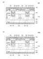
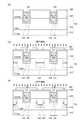
従来より、トレンチゲートパワーMOSFETは、DC−DCコンバーターなど各種電源装置に広く用いられている(例えば、特許文献1参照。)。図12は、従来のトレンチゲートパワーMOSFET900を説明するために示す図である。 Conventionally, trench gate power MOSFETs have been widely used in various power supply devices such as DC-DC converters (see, for example, Patent Document 1). FIG. 12 is a diagram for explaining a conventional trench
従来のトレンチゲートパワーMOSFET900は、図12に示すように、n+型のドレイン層912と、ドレイン層912上に位置するn−型のドリフト層914と、ドリフト層914上に位置するp型のボディ層920と、ボディ層920を開口し、ドリフト層914に達して形成してなる溝924と、ボディ層920内に配置されるとともに、少なくとも一部を溝924の内周面に露出させて形成してなるn+型のソース領域932と、溝924の内周面に形成してなるゲート絶縁膜926と、ゲート絶縁膜926の内周面に形成してなるゲート電極層928と、ゲート電極層928と絶縁されるとともに、ソース領域932と接して形成してなるソース電極層(図示せず。)とを備える。そして、従来のトレンチゲートパワーMOSFET900においては、ドリフト層914において隣接する溝924に挟まれた領域には、溝よりも深く延在するp+型埋め込み領域940がボディ層920から下方に突出するように形成されている。なお、図12中、符号934はp+型コンタクト領域を示す。As shown in FIG. 12, a conventional trench
従来のトレンチゲートパワーMOSFET900によれば、通常のプレーナゲートパワーMOSFETの場合よりも単位セル面積を縮小することが可能であるため、通常のプレーナゲートパワーMOSFETの場合よりもオン抵抗を低減することが可能となる。
また、従来のトレンチゲートパワーMOSFET900によれば、ドリフト層914において隣接する溝924に挟まれた領域には、溝よりも深く延在するp+型埋め込み領域940がボディ層920から下方に突出するように形成されているため、逆バイアス時においては溝924の底面近傍における電界が緩和され、逆耐圧を高くすることが可能となる。According to the conventional trench
Further, according to the conventional trench
しかしながら、従来のトレンチゲートパワーMOSFET900においては、p+型埋め込み領域940の存在に起因して順バイアス時にオン電流が流れる領域が狭くなるため、より一層オン抵抗を低くすることが困難であるという問題がある。However, in the conventional trench
なお、このような問題は、pとnとを逆にしたトレンチゲートパワーMOSFETの場合にも同様に見られる問題である。また、このような問題はトレンチゲートパワーMOSFETの場合だけに存在する問題ではなく、トレンチゲートIGBTその他のトレンチゲートパワー半導体装置全般に存在する問題である。 Such a problem is also seen in the case of a trench gate power MOSFET in which p and n are reversed. Such a problem is not a problem that exists only in the case of the trench gate power MOSFET, but a problem that exists in the trench gate IGBT and other trench gate power semiconductor devices in general.
そこで、本発明は、上記した問題を解決するためになされたもので、高い逆耐圧を有するとともにより一層オン抵抗を低くすることが可能なトレンチゲートパワー半導体装置を提供することを目的とする。 Accordingly, the present invention has been made to solve the above-described problems, and an object of the present invention is to provide a trench gate power semiconductor device that has a high reverse breakdown voltage and can further reduce the on-resistance.
[1]本発明のトレンチゲートパワー半導体装置は、第1導電型のドリフト層と、前記ドリフト層上に位置し、前記第1導電型とは反対の第2導電型のボディ層と、前記ボディ層を開口し、前記ドリフト層に達して形成してなる溝と、前記ボディ層内に配置されるとともに、少なくとも一部を前記溝の内周面に露出させて形成してなる第1導電型の第1半導体領域と、前記溝の内周面に形成してなるゲート絶縁膜と、前記ゲート絶縁膜の内周面に形成してなるゲート電極膜と、前記ゲート電極膜と絶縁されるとともに、前記第1半導体領域と接して形成してなる第1電極層とを備え、前記ドリフト層において隣接する前記溝に挟まれた領域には、前記溝よりも深く延在する第2導電型の埋め込み領域が前記ボディ層に接するように形成され、前記埋め込み領域における第2導電型不純物が最大濃度を示す深さ位置が、前記ボディ層の底面と前記埋め込み領域の底面との中間に位置する深さ位置よりも深いところにあることを特徴とする。[1] A trench gate power semiconductor device according to the present invention includes a first conductivity type drift layer, a second conductivity type body layer located on the drift layer and opposite to the first conductivity type, and the body A groove formed by opening a layer and reaching the drift layer, and a first conductivity type formed by being disposed in the body layer and exposing at least a part of the inner peripheral surface of the groove The first semiconductor region, the gate insulating film formed on the inner peripheral surface of the trench, the gate electrode film formed on the inner peripheral surface of the gate insulating film, and the gate electrode film. A first electrode layer formed in contact with the first semiconductor region, and a region of a second conductivity type extending deeper than the groove in a region sandwiched between the adjacent grooves in the drift layer. An embedded region is formed in contact with the body layer; The depth position where the second conductivity type impurity in the buried region has the maximum concentration is deeper than the depth position located between the bottom surface of the body layer and the bottom surface of the buried region. .
[2]本発明のトレンチゲートパワー半導体装置においては、前記ドリフト層における前記埋め込み領域の周囲には、前記埋め込み領域を覆うように、前記ドリフト層よりも高濃度の第1導電型不純物を含有する高濃度第1導電型半導体領域が形成されていることが好ましい。[2] In the trench gate power semiconductor device of the present invention, the periphery of the buried region in the drift layer contains a first conductivity type impurity having a concentration higher than that of the drift layer so as to cover the buried region. It is preferable that a high concentration first conductivity type semiconductor region is formed.
[3]本発明のトレンチゲートパワー半導体装置においては、前記溝の底面の深さ位置が、前記ボディ層の底面と前記ドリフト層の底面との中間に位置する深さ位置よりも深いところにあることが好ましい。[3] In the trench gate power semiconductor device of the present invention, the depth position of the bottom surface of the groove is deeper than the depth position located between the bottom surface of the body layer and the bottom surface of the drift layer. It is preferable.
[4]本発明のトレンチゲートパワー半導体装置においては、前記トレンチゲートパワー半導体装置は、トレンチゲートパワーMOSFETであり、前記第1半導体領域は、ソース領域であり、前記第1電極層は、ソース電極層であり、前記第1導電型のドリフト層は、第1導電型のドレイン層上に配置されていることが好ましい。[4] In the trench gate power semiconductor device of the present invention, the trench gate power semiconductor device is a trench gate power MOSFET, the first semiconductor region is a source region, and the first electrode layer is a source electrode. Preferably, the first conductivity type drift layer is disposed on the first conductivity type drain layer.
[5]本発明のトレンチゲートパワー半導体装置においては、前記トレンチゲートパワー半導体装置は、トレンチゲートIGBTであり、前記第1半導体領域は、エミッタ領域であり、前記第1電極層は、エミッタ電極層であり、前記第1導電型のドリフト層は、第2導電型のコレクタ層上に配置されていることが好ましい。[5] In the trench gate power semiconductor device of the present invention, the trench gate power semiconductor device is a trench gate IGBT, the first semiconductor region is an emitter region, and the first electrode layer is an emitter electrode layer. The first conductivity type drift layer is preferably disposed on the second conductivity type collector layer.
[6]本発明のトレンチゲートパワー半導体装置の製造方法は、本発明のトレンチゲートパワー半導体装置(上記[1]〜[5]のいずれかに記載のトレンチゲートパワー半導体装置)を製造するためのトレンチゲートパワー半導体装置の製造方法であって、高エネルギーイオン注入装置を用いた多段階イオン注入法により前記ドリフト層の所定領域に第2導電型不純物をイオン注入して、前記埋め込み領域を形成することを特徴とする。[6] A method for manufacturing a trench gate power semiconductor device according to the present invention is for manufacturing the trench gate power semiconductor device according to the present invention (the trench gate power semiconductor device according to any one of [1] to [5] above). A method of manufacturing a trench gate power semiconductor device, wherein a second conductivity type impurity is ion-implanted into a predetermined region of the drift layer by a multi-stage ion implantation method using a high energy ion implanter to form the buried region. It is characterized by that.
[7]本発明のトレンチゲートパワー半導体装置の製造方法は、本発明のトレンチゲートパワー半導体装置(上記[2]に記載のトレンチゲートパワー半導体装置)を製造するためのトレンチゲートパワー半導体装置の製造方法であって、高エネルギーイオン注入装置を用いたイオン注入法により前記ドリフト層の所定領域に第1導電型不純物をイオン注入するとともに、高エネルギーイオン注入装置を用いた多段階イオン注入法により前記ドリフト層の所定領域に第2導電型不純物をイオン注入することにより、前記高濃度第1導電型半導体領域及び前記埋め込み領域を形成することを特徴とする。[7] A method for manufacturing a trench gate power semiconductor device according to the present invention is a method for manufacturing a trench gate power semiconductor device for manufacturing the trench gate power semiconductor device according to the present invention (the trench gate power semiconductor device according to [2] above). A first conductivity type impurity is ion-implanted into a predetermined region of the drift layer by an ion implantation method using a high-energy ion implantation apparatus, and a multi-stage ion implantation method using a high-energy ion implantation apparatus. The high-concentration first conductive semiconductor region and the buried region are formed by ion-implanting a second conductive impurity into a predetermined region of the drift layer.
本発明のトレンチゲートパワー半導体装置によれば、埋め込み領域における第2導電型不純物が最大濃度を示す深さ位置が、ボディ層の底面と埋め込み領域の底面との中間に位置する深さ位置よりも深いところにあるため、後述する図2に示すように、逆バイアス時においては溝の底面近傍における電界がより一層緩和されるようになり、従来のトレンチゲートパワーMOSFET900の場合よりも一層逆耐圧を高くすることが可能となる。 According to the trench gate power semiconductor device of the present invention, the depth position where the second conductivity type impurity in the buried region has the maximum concentration is more than the depth position located between the bottom surface of the body layer and the bottom surface of the buried region. As shown in FIG. 2 to be described later, the electric field in the vicinity of the bottom surface of the groove is further relaxed during reverse bias, and the reverse breakdown voltage is further improved as compared with the case of the conventional trench
このため、逆耐圧を維持したままドリフト領域の不純物濃度を高くすることが可能となるため、従来のトレンチゲートパワーMOSFETの場合よりも一層オン抵抗を低くすることが可能となる。従って、本発明のトレンチゲートパワー半導体装置は、高い逆耐圧を有するとともにより一層オン抵抗を低くすることが可能なトレンチゲートパワー半導体装置となる。 For this reason, since it is possible to increase the impurity concentration of the drift region while maintaining the reverse breakdown voltage, the on-resistance can be further reduced as compared with the case of the conventional trench gate power MOSFET. Therefore, the trench gate power semiconductor device of the present invention is a trench gate power semiconductor device that has a high reverse breakdown voltage and can further reduce the on-resistance.
本発明のトレンチゲートパワー半導体装置の製造方法(上記[6]に記載のトレンチゲートパワー半導体装置の製造方法)によれば、本発明のトレンチゲートパワー半導体装置(上記[1]〜[5]のいずれかに記載のトレンチゲートパワー半導体装置)を製造することができる。 According to the manufacturing method of the trench gate power semiconductor device of the present invention (the manufacturing method of the trench gate power semiconductor device of [6] above), the trench gate power semiconductor device of the present invention (of [1] to [5] above). Any one of the trench gate power semiconductor devices) can be manufactured.
本発明のトレンチゲートパワー半導体装置の製造方法(上記[7]に記載のトレンチゲートパワー半導体装置の製造方法)によれば、本発明のトレンチゲートパワー半導体装置(上記[2]に記載のトレンチゲートパワー半導体装置)を製造することができる。 According to the method of manufacturing a trench gate power semiconductor device of the present invention (the method of manufacturing the trench gate power semiconductor device of [7] above), the trench gate power semiconductor device of the present invention (trench gate according to [2] above). Power semiconductor device) can be manufactured.
以下、本発明のトレンチゲートパワー半導体装置及びその製造方法について、図に示す実施の形態に基づいて説明する。 Hereinafter, a trench gate power semiconductor device and a manufacturing method thereof according to the present invention will be described based on embodiments shown in the drawings.
[実施形態1]
1.実施形態1に係るトレンチゲートパワー半導体装置100
図1は、実施形態1に係るトレンチゲートパワー半導体装置100を説明するために示す図である。図1(a)はトレンチゲートパワー半導体装置100の断面図であり、図1(b)はトレンチゲートパワー半導体装置100におけるp不純物及びn不純物の濃度プロファイルを示す図である。[Embodiment 1]
1. Trench gate
FIG. 1 is a view for explaining a trench gate
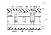
実施形態1に係るトレンチゲートパワー半導体装置100は、図1(a)に示すように、n−型のドリフト層114と、ドリフト層114上に位置するp型のボディ層120と、ボディ層120を開口し、ドリフト層114に達して形成してなる溝124と、ボディ層120内に配置されるとともに、少なくとも一部を溝124の内周面に露出させて形成してなるn+型のソース領域(第1半導体領域)132と、溝124の内周面に形成してなるゲート絶縁膜126と、ゲート絶縁膜126の内周面に形成してなるゲート電極膜128と、ゲート電極膜128と絶縁されるとともに、ソース領域132と接して形成してなるソース電極層(第1電極層)136とを備えるトレンチゲートパワーMOSFETである。As shown in FIG. 1A, the trench gate
そして、実施形態1に係るトレンチゲートパワー半導体装置100においては、ドリフト層114において隣接する溝124に挟まれた領域には、溝124よりも深く延在するp型の埋め込み領域140がボディ層120に接するように形成されており、埋め込み領域140におけるp型不純物が最大濃度を示す深さ位置Pが、図1(a)及び図1(b)に示すように、ボディ層120の底面P2と埋め込み領域140の底面P3との中間に位置する深さ位置よりも深いところにある。なお、図1(a)中、符号110は半導体基体を示し、符号130は保護絶縁膜を示し、符号134はp+型のコンタクト領域を示し、符号112はn+型のドレイン層を示し、符号138はドレイン電極層を示す。In the trench gate
ドレイン層112の厚さは例えば300μmであり、ドレイン層112の不純物濃度は例えば2×1019cm−3である。また、ドリフト層114の厚さは例えば20μmであり、ドリフト層114の不純物濃度は例えば1×1015cm−3である。また、ボディ層120の厚さは例えば1.5μmであり、ボディ層120の不純物濃度は、表面において例えば1×1017cm−3である。The
溝の深さは例えば2μmである。ソース領域132の深さは例えば0.3μmであり、ソース領域132の不純物濃度は例えば2×1019cm−3である。コンタクト領域134の深さは例えば1μmであり、コンタクト領域134の不純物濃度は例えば2×1019cm−3である。ゲート絶縁膜126の厚さは例えば0.1μmである。ゲート電極層128は例えばリンをドープしたポリシリコンからなる。ソース電極層136は、例えばアルミニウムからなり、厚さが例えば5μmである。ソース電極層136は保護絶縁膜130によりゲート電極層128と絶縁されている。ドレイン電極層138は、例えばニッケルからなり、厚さが例えば2μmである。The depth of the groove is 2 μm, for example. The depth of the
埋め込み領域140の底面P3の深さ位置は、ボディ層120の底面P2から5μmだけ深い位置にある。そして、埋め込み領域140におけるp型不純物が最大濃度を示す深さ位置Pは、ボディ層120の底面P2から3μmだけ深い位置にある。従って、埋め込み領域140におけるp型不純物が最大濃度を示す深さ位置Pは、ボディ層120の底面P2と埋め込み領域140の底面P3との中間に位置する深さ位置よりも深いところにある。 The depth position of the bottom surface P3 of the buried
2.実施形態1に係るトレンチゲートパワー半導体装置100の効果
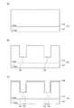
図2は、逆バイアス時における電位分布を模式的に示す図である。図2(a)は実施形態1に係るトレンチゲートパワー半導体装置100における逆バイアス時の電位分布を模式的に示す図であり、図2(b)は比較例に係るトレンチゲートパワー半導体装置100aにおける逆バイアス時の電位分布を模式的に示す図である。実施形態1に係るトレンチゲートパワー半導体装置100は、後述する「実施形態1に係るトレンチゲートパワー半導体装置100を製造する方法」により製造する。また、比較例に係るトレンチゲートパワー半導体装置100aは、後述する「比較例に係るトレンチゲートパワー半導体装置100aを製造する方法」方法により製造する。なお、図2中、等電位線を破線で示す。2. Effect of Trench Gate
実施形態1に係るトレンチゲートパワー半導体装置100によれば、図1(b)に示すように、埋め込み領域140におけるp型不純物が最大濃度を示す深さ位置Pが、ボディ層120の底面P2と埋め込み領域140の底面との中間に位置する深さ位置よりも深いところにあるため、図2に示すように、逆バイアス時においては溝124の底面近傍における電界がより一層緩和されるようになり、従来のトレンチゲートパワーMOSFET900の場合よりも一層逆耐圧を高くすることが可能となる。このため、実施形態1に係るトレンチゲートパワー半導体装置100によれば、逆耐圧を維持したままドリフト領域の不純物濃度を高くすることが可能となるため、従来のトレンチゲートパワーMOSFETの場合よりも一層オン抵抗を低くすることが可能となる。 According to the trench gate
従って、実施形態1に係るトレンチゲートパワー半導体装置100は、高い逆耐圧を有するとともにより一層オン抵抗を低くすることが可能なトレンチゲートパワー半導体装置となる。 Therefore, the trench gate
3.実施形態1に係るトレンチゲートパワー半導体装置100を製造する方法
実施形態1に係るトレンチゲートパワー半導体装置100は、以下のような方法により製造することができる。3. Method of Manufacturing Trench Gate
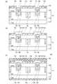
図3〜図7は、実施形態1に係るトレンチゲートパワー半導体装置の製造方法を説明するために示す図である。図3(a)〜図3(c)、図4(a)〜図4(c)、図5(a)〜図5(c)、図6(a)〜図6(c)及び図7(a)〜図7(c)は各工程図である。 3 to 7 are views for explaining the method of manufacturing the trench gate power semiconductor device according to the first embodiment. 3A to FIG. 3C, FIG. 4A to FIG. 4C, FIG. 5A to FIG. 5C, FIG. 6A to FIG. 6C, and FIG. (A)-FIG.7 (c) are each process drawing.
(1)半導体基体準備工程
図3(a)に示すように、ドレイン層112となるn+型半導体基板と、ドリフト層114及びボディ層120となるn−型エピタキシャル層113とが積層された構造の半導体基体110を準備する。(1) Semiconductor Substrate Preparation Step As shown in FIG. 3A, a structure in which an n+ type semiconductor substrate to be the
(2)溝形成工程
その後、図3(b)に示すように、n−型エピタキシャル層113の表面から所定深さの溝124を形成する。溝の深さは例えば2μmとする。(2) Groove Formation Step Thereafter, as shown in FIG. 3B, a
(3)ゲート絶縁膜形成工程
その後、酸化性雰囲気の下で半導体基体110に熱処理を施して、図3(c)に示すように、n−型エピタキシャル層113の表面及び溝124の内周面(底面及び側面)に熱酸化膜126,126’を形成する。当該熱酸化膜126,126’のうち溝124の内周面(底面及び側面)に形成された熱酸化膜126がゲート絶縁膜126となる。(3) Gate insulating film forming step Thereafter, the
(4)ゲート電極層形成工程
その後、図4(a)に示すように、n−型エピタキシャル層113の表面側から、溝124を埋めるようにドープトポリシリコン膜128’を形成する。
その後、図4(b)に示すように、ポリシリコン膜128’のエッチバックを行い、溝124の内部にのみポリシリコン膜128’を残した状態でポリシリコン膜128’を除去する。これにより、溝124の内周面にゲート電極層128が形成される。(4) Gate Electrode Layer Formation Step Thereafter, as shown in FIG. 4A, a doped
Thereafter, as shown in FIG. 4B, the
(5)p型ボディ層形成工程
その後、図4(c)に示すように、n−型エピタキシャル層113の表面側からイオン注入法によりp型不純物(例えばボロンイオン)をイオン注入する。イオン注入は、比較的低い加速電圧(例えば100eV)かつ比較的低ドーズ量(例えば1×1013cm−2)の条件にて行う。
次に、半導体基体110に熱処理(例えば1000℃、1時間)を施してp型不純物を拡散及び活性化させることにより、図5(a)に示すように、ボディ層120を形成する。(5) P-type body layer forming step Thereafter, as shown in FIG. 4C, p-type impurities (for example, boron ions) are ion-implanted from the surface side of the n− -
Next, heat treatment (for example, 1000 ° C., 1 hour) is performed on the
(6)埋め込み層を形成するためのイオン注入工程
その後、ボディ層120の表面における所定領域にマスクM1を形成した後、当該マスクM1を介して、図5(b)、図5(c)及び図6(a)に示すように、n−型エピタキシャル層113の表面側から多段階イオン注入法によりp型不純物(例えばボロンイオン)をイオン注入する。この工程は、まず、第1の加速電圧(例えば600keV)かつ第1のドーズ量(例えば1×1013cm−2)の条件でボロンイオンを注入し、その後、第2の加速電圧(例えば550keV)かつ第2のドーズ量(例えば3×1012cm−2)の条件でボロンイオンを注入し、その後、第3の加速電圧(例えば500keV)かつ第2のドーズ量(例えば1×1012cm−2)の条件でボロンイオンを注入することにより行う。(6) Ion Implantation Step for Forming Buried Layer Subsequently, after forming a mask M1 in a predetermined region on the surface of the
(7)コンタクト領域を形成するためのイオン注入工程
その後、図6(b)に示すように、マスクM1をつけたまま、当該マスクM1を介してp型不純物(例えばボロンイオン)のイオン注入を行う。この工程は、比較的低い加速電圧(例えば50keV)かつ比較的高いドーズ量(例えば5×1015cm−2)の条件でボロンイオンを注入することにより行う。(7) Ion Implantation Step for Forming Contact Region Thereafter, as shown in FIG. 6B, ion implantation of p-type impurities (for example, boron ions) is performed through the mask M1 while the mask M1 is attached. Do. This step is performed by implanting boron ions under conditions of a relatively low acceleration voltage (for example, 50 keV) and a relatively high dose (for example, 5 × 1015 cm−2 ).
(8)ソース領域を形成するためのイオン注入工程
その後、図6(c)に示すように、ボディ層120の表面からマスクM1を除去し、ボディ層120の表面における所定領域にマスクM2を形成した後、当該マスクM2を介してn型不純物(例えばヒ素イオン)のイオン注入を行う。この工程は、比較的低い加速電圧(例えば50keV)かつ比較的高いドーズ量(例えば1×1015cm−2)の条件でヒ素イオンを注入することにより行う。(8) Ion Implantation Step for Forming Source Region Thereafter, as shown in FIG. 6C, the mask M1 is removed from the surface of the
(9)不純物イオン活性化工程
その後、半導体基体110に熱処理を施してn型不純物及びp型不純物を活性化させる。これにより、図7(a)に示すように、ボディ層120内にソース領域132及びコンタクト領域134が形成されるとともにドリフト層114内に図1(b)に示すような濃度プロファイルを有する埋め込み領域140が形成される。(9) Impurity ion activation process Thereafter, the
(10)保護絶縁膜形成工程
その後、ボディ層120の表面における熱酸化膜126’を除去した後、半導体基体110に熱処理を施してボディ層120の表面及び溝124上部の内周面にシリコンの熱酸化膜を形成し、その後、ボディ層120の表面側から気相法によりPSG膜を形成することにより積層膜を形成し、さらにその後、ゲート電極層128の上部を残して積層膜をエッチングにより除去する。これにより、図7(b)に示すように、ゲート電極層128の上部に保護絶縁膜130が形成される。(10) Step of forming a protective insulating film Thereafter, after removing the
(11)ソース電極層形成工程及びドレイン電極層形成工程
その後、図7(c)に示すように、ボディ層120及び保護絶縁膜130を覆うようにソース電極層136を形成し、n+型ドレイン層112の表面にドレイン電極層138を形成する。(11) Source electrode layer forming step and drain electrode layer forming step Thereafter, as shown in FIG. 7C, a
以上のようにして、実施形態1に係るトレンチゲートパワー半導体装置100を製造することができる。 As described above, the trench gate
4.比較例に係るトレンチゲートパワー半導体装置100aを製造する方法
比較例に係るトレンチゲートパワー半導体装置100aは、「埋め込み層を形成するためのイオン注入工程」以外の工程は、実施形態1に係るトレンチゲートパワー半導体装置100を製造する方法と同様の方法により製造する。そして、「埋め込み層を形成するためのイオン注入工程」は、以下のようにして行う。4). Method of Manufacturing Trench Gate
(6’)埋め込み層を形成するためのイオン注入工程
その後、ボディ層120の表面における所定領域にマスクM1を形成した後、当該マスクM1を介して、n−型エピタキシャル層113の表面側から多段階イオン注入法によりp型不純物(例えばボロンイオン)をイオン注入する。この工程は、まず、第1の加速電圧(例えば600keV)かつ所定のドーズ量(例えば3×1012cm−2)の条件でボロンイオンを注入し、その後、第2の加速電圧(例えば550keV)かつ上記した所定のドーズ量(例えば3×1012cm−2)の条件でボロンイオンを注入し、その後、第3の加速電圧(例えば500keV)かつ上記した所定のドーズ量(例えば3×1012cm−2)の条件でボロンイオンを注入することにより行う。(6 ′) Ion Implantation Step for Forming Buried Layer After that, a mask M1 is formed in a predetermined region on the surface of the
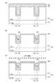
[実施形態2]
図8は、実施形態2に係るトレンチゲートパワー半導体装置102を説明するために示す図である。図8(a)はトレンチゲートパワー半導体装置102の断面図であり、図8(b)はトレンチゲートパワー半導体装置102におけるp不純物及びn不純物の濃度プロファイルを示す図である。図9は、実施形態2に係るトレンチゲートパワー半導体装置102を製造する方法を説明するために示す図である。図9(a)〜図9(c)は主要な工程を示す図である。なお、図9(a)は図5(a)に対応する図であり、図9(c)は図5(b)に対応する図である。[Embodiment 2]
FIG. 8 is a view for explaining the trench gate
実施形態2に係るトレンチゲートパワー半導体装置102は、基本的には実施形態1に係るトレンチゲートパワー半導体装置100と同様の構成を有するが、図8に示すように、ドリフト層114における埋め込み領域140の周囲には、埋め込み領域140を覆うように、ドリフト層114よりも高濃度のn型不純物を含有するn+型半導体領域142が形成されている点で実施形態1に係るトレンチゲートパワー半導体装置100とは異なる。The trench gate
このように、実施形態2に係るトレンチゲートパワー半導体装置102は、上記したようなn+型半導体領域142が形成されている点で実施形態1に係るトレンチゲートパワー半導体装置100とは異なるが、実施形態1に係るトレンチゲートパワー半導体装置100の場合と同様に、上記した構造の埋め込み領域140を備えるため、高い逆耐圧を有するとともにより一層オン抵抗を低くすることが可能なトレンチゲートパワー半導体装置となる。Thus, the trench gate
また、実施形態2に係るトレンチゲートパワー半導体装置102によれば、埋め込み領域140を覆うようにn+型半導体領域142が形成されているため、ドリフト層114においてオン電流が流れる領域にp型不純物が拡散することが極力抑制され、より一層オン抵抗を低くすることが可能となる。Further, according to the trench gate
なお、実施形態2に係るトレンチゲートパワー半導体装置102は、埋め込み領域140を覆うようにn+型半導体領域142が形成されている点以外の点については、実施形態1に係るトレンチゲートパワー半導体装置100と同様の構成を有するため、実施形態1に係るトレンチゲートパワー半導体装置100が有する効果のうち該当する効果を有する。The trench gate
実施形態2に係るトレンチゲートパワー半導体装置102は、実施形態1に係るトレンチゲートパワー半導体装置100の製造方法とほぼ同様の工程により製造することができる。但し、図9に示すように、p型ボディ層形成工程と、埋め込み層を形成するためのイオン注入工程との間に、埋め込み領域140を覆うこととなる領域(埋め込み領域140よりも若干大きめ領域)にn+型半導体領域を形成するためのイオン注入工程をさらに備える。当該イオン注入工程は、高エネルギーイオン注入装置を用いて行うことができる。これにより、図8に示す実施形態2に係るトレンチゲートパワー半導体装置102を製造することができる。The trench gate
[実施形態3]
図10は、実施形態3に係るトレンチゲートパワー半導体装置104の断面図である。実施形態3に係るトレンチゲートパワー半導体装置104は、基本的には実施形態1に係るトレンチゲートパワー半導体装置100と同様の構成を有するが、溝124の底面の深さ位置が実施形態1に係るトレンチゲートパワー半導体装置100とは異なる。すなわち、実施形態3に係るトレンチゲートパワー半導体装置104においては、図10に示すように、溝124の底面の深さ位置が、ボディ層120の底面とドリフト層114の底面との中間に位置する深さ位置よりも深いところにある。[Embodiment 3]
FIG. 10 is a cross-sectional view of the trench gate
このように、実施形態3に係るトレンチゲートパワー半導体装置104は、溝124の底面の深さ位置が実施形態1に係るトレンチゲートパワー半導体装置100の場合とは異なるが、実施形態1に係るトレンチゲートパワー半導体装置100の場合と同様に、上記した構造の埋め込み領域140を備えるため、高い逆耐圧を有するとともにより一層オン抵抗を低くすることが可能なトレンチゲートパワー半導体装置となる。 As described above, the trench gate
また、実施形態3に係るトレンチゲートパワー半導体装置102によれば、溝124の底面の深さ位置が、ボディ層120の底面とドリフト層114の底面との中間に位置する深さ位置よりも深いところにあるため、実施形態1に係るトレンチゲートパワー半導体装置100の場合と同様に、従来よりもオン抵抗をより一層低減することが可能となる。 In addition, according to the trench gate
なお、実施形態3に係るトレンチゲートパワー半導体装置102においては、実施形態2に係るトレンチゲートパワー半導体装置102の場合と同様に、ドリフト層114における埋め込み領域140の周囲には、埋め込み領域140を覆うように、ドリフト層114よりも高濃度のn型不純物を含有するn+型半導体領域142が形成されていてもよい。この場合には、溝124の底面の深さ位置をボディ層120の底面とドリフト層114の底面との中間に位置する深さ位置よりも深いところにしたとしても、逆耐圧が低減してしまうこともない。In the trench gate
なお、実施形態3に係るトレンチゲートパワー半導体装置104は、溝124の底面の深さ位置以外の点については、実施形態1に係るトレンチゲートパワー半導体装置100と同様の構成を有するため、実施形態1に係るトレンチゲートパワー半導体装置100が有する効果のうち該当する効果を有する。 The trench gate
以上、本発明のトレンチゲートパワー半導体装置を上記の実施形態に基づいて説明したが、本発明はこれに限定されるものではなく、その要旨を逸脱しない範囲において実施することが可能であり、例えば、次のような変形も可能である。 As described above, the trench gate power semiconductor device of the present invention has been described based on the above embodiment, but the present invention is not limited to this, and can be implemented without departing from the scope of the present invention. The following modifications are also possible.
(1)上記した実施形態1においては、3段階のイオン注入により多段階イオン注入法を行ったが、本発明はこれに限定されるものではない。2段階のイオン注入により多段階イオン注入法を行ってもよいし、4段階以上のイオン注入により多段階イオン注入法を行ってもよい。(1) In Embodiment 1 described above, the multi-stage ion implantation method is performed by three-stage ion implantation, but the present invention is not limited to this. The multistage ion implantation method may be performed by two-stage ion implantation, or the multistage ion implantation method may be performed by four or more stages of ion implantation.
(2)上記した各実施形態においては、トレンチゲートパワーMOSFETを例にとって本発明のトレンチゲートパワー半導体装置を説明したが、本発明はこれに限定されるものではない。図11は、変形例に係るトレンチゲートパワー半導体装置200の断面図である。図11に示すように、本発明は、例えばトレンチゲートIGBTにも適用可能である。(2) In each of the above-described embodiments, the trench gate power semiconductor device of the present invention has been described by taking the trench gate power MOSFET as an example. However, the present invention is not limited to this. FIG. 11 is a cross-sectional view of a trench gate
(3)上記した各実施形態においては、第1導電型をn型とし第2導電型をp型として、本発明の半導体装置を説明したが、本発明はこれに限定されるものではない。例えば、第1導電型をp型とし第2導電型をn型としてもよい。(3) In each of the above embodiments, the semiconductor device of the present invention has been described with the first conductivity type as n-type and the second conductivity type as p-type. However, the present invention is not limited to this. For example, the first conductivity type may be p-type and the second conductivity type may be n-type.
100,102,104,200…トレンチゲートパワー半導体装置、110,210,910…半導体基体、112,912…ドレイン層、113…n−型エピタキシャル層、114,214,914…ドリフト層、120,220,920…ボディ層、124,224,924…溝、126,226,926…ゲート絶縁膜、126’…シリコン酸化膜、128’…ポリシリコン層、128,228,928…ゲート電極層、130,230,930…保護絶縁膜、132,932…ソース領域、134,234,934…コンタクト領域、136,936…ソース電極層、138,938…ドレイン電極層、140,240…埋め込み領域、142…n+型半導体領域、212…コレクタ層、232…エミッタ領域、236…エミッタ電極層、238…コレクタ電極層、900…トレンチゲートパワーMOSFET100, 102, 104, 200 ... trench gate power semiconductor device, 110, 210, 910 ... semiconductor substrate, 112, 912 ... drain layer, 113 ... n- type epitaxial layer, 114, 214, 914 ... drift layer, 120, 220 , 920 ... body layer, 124, 224, 924 ... groove, 126, 226, 926 ... gate insulating film, 126 '... silicon oxide film, 128' ... polysilicon layer, 128, 228, 928 ... gate electrode layer, 130, 230, 930 ... protective insulating film, 132, 932 ... source region, 134, 234, 934 ... contact region, 136, 936 ... source electrode layer, 138, 938 ... drain electrode layer, 140, 240 ... buried region, 142 ... n+ Type semiconductor region 212 ...
Claims (5)
Translated fromJapanese前記ドリフト層上に位置し、前記第1導電型とは反対の第2導電型のボディ層と、
前記ボディ層を開口し、前記ドリフト層に達して形成してなる溝と、
前記ボディ層内に配置されるとともに、少なくとも一部を前記溝の内周面に露出させて形成してなる第1導電型の第1半導体領域と、
前記溝の内周面に形成してなるゲート絶縁膜と、
前記ゲート絶縁膜の内周面に形成してなるゲート電極膜と、
前記ゲート電極膜と絶縁されるとともに、前記第1半導体領域と接して形成してなる第1電極層とを備え、
前記ドリフト層において隣接する前記溝に挟まれた領域には、前記溝よりも深く延在する第2導電型の埋め込み領域が前記ボディ層に接するように形成され、
前記埋め込み領域における第2導電型不純物が最大濃度を示す深さ位置が、前記ボディ層の底面と前記埋め込み領域の底面との中間に位置する深さ位置よりも深いところにあるトレンチゲートパワー半導体装置であって、
前記ドリフト層における前記埋め込み領域の周囲には、前記埋め込み領域を覆うように、前記ドリフト層よりも高濃度の第1導電型不純物を含有する高濃度第1導電型半導体領域が形成され、
前記高濃度第1導電型半導体領域は、前記ドリフト層に前記第2導電型不純物が拡散することを抑制すべく前記埋め込み領域の周囲に形成されていることを特徴とするトレンチゲートパワー半導体装置。A first conductivity type drift layer;
A body layer of a second conductivity type located on the drift layer and opposite to the first conductivity type;
A groove formed by opening the body layer and reaching the drift layer;
A first semiconductor region of a first conductivity type disposed in the body layer and formed by exposing at least a part of the inner peripheral surface of the groove;
A gate insulating film formed on the inner peripheral surface of the groove;
A gate electrode film formed on the inner peripheral surface of the gate insulating film;
A first electrode layer that is insulated from the gate electrode film and formed in contact with the first semiconductor region;
In the region sandwiched between the adjacent grooves in the drift layer, a buried region of a second conductivity type extending deeper than the groove is formed so as to be in contact with the body layer,
A trench gate power semiconductor device in which a depth position where the second conductivity type impurity in the buried region has a maximum concentration is deeper than a depth position located between the bottom surface of the body layer and the bottom surface of the buried region. Because
Around the buried region in the drift layer, a high concentration first conductivity type semiconductor region containing a first conductivity type impurity having a concentration higher than that of the drift layer is formed so as to cover the buried region,
The trench gate power semiconductor device,wherein the high-concentration first conductivity type semiconductor region is formed around the buried region to suppress diffusion of the second conductivity type impurity into the drift layer .
前記溝の底面の深さ位置が、前記ボディ層の底面と前記ドリフト層の底面との中間に位置する深さ位置よりも深いところにあることを特徴とするトレンチゲートパワー半導体装置。The trench gate power semiconductor device according to claim 1,
The trench gate power semiconductor device, wherein a depth position of the bottom surface of the groove is deeper than a depth position located between the bottom surface of the body layer and the bottom surface of the drift layer.
前記トレンチゲートパワー半導体装置は、トレンチゲートパワーMOSFETであり、
前記第1半導体領域は、ソース領域であり、
前記第1電極層は、ソース電極層であり、
前記第1導電型のドリフト層は、第1導電型のドレイン層上に配置されていることを特徴とするトレンチゲートパワー半導体装置。In the trench gate power semiconductor device according to claim 1 or 2,
The trench gate power semiconductor device is a trench gate power MOSFET,
The first semiconductor region is a source region;
The first electrode layer is a source electrode layer;
The trench gate power semiconductor device, wherein the first conductivity type drift layer is disposed on the first conductivity type drain layer.
前記トレンチゲートパワー半導体装置は、トレンチゲートIGBTであり、
前記第1半導体領域は、エミッタ領域であり、
前記第1電極層は、エミッタ電極層であり、
前記第1導電型のドリフト層は、第2導電型のコレクタ層上に配置されていることを特徴とするトレンチゲートパワー半導体装置。In the trench gate power semiconductor device according to claim 1 or 2,
The trench gate power semiconductor device is a trench gate IGBT,
The first semiconductor region is an emitter region;
The first electrode layer is an emitter electrode layer;
The trench gate power semiconductor device, wherein the first conductivity type drift layer is disposed on a second conductivity type collector layer.
高エネルギーイオン注入装置を用いたイオン注入法により前記ドリフト層の所定領域に第1導電型不純物をイオン注入するとともに、高エネルギーイオン注入装置を用いた多段階イオン注入法により前記ドリフト層の所定領域に第2導電型不純物をイオン注入することにより、前記高濃度第1導電型半導体領域及び前記埋め込み領域を形成することを特徴とするトレンチゲートパワー半導体装置の製造方法。A method of manufacturing a trench gate power semiconductor device for manufacturing the trench gate power semiconductor device according to claim 1,
The first conductivity type impurity is ion-implanted into the predetermined region of the drift layer by an ion implantation method using a high energy ion implantation apparatus, and the predetermined region of the drift layer is formed by a multi-stage ion implantation method using a high energy ion implantation apparatus. A method of manufacturing a trench gate power semiconductor device, wherein the second conductivity type impurity is ion-implanted to form the high-concentration first conductivity type semiconductor region and the buried region.
Priority Applications (1)
| Application Number | Priority Date | Filing Date | Title |
|---|---|---|---|
| JP2012540208AJP5554417B2 (en) | 2011-05-27 | 2012-05-25 | Trench gate power semiconductor device and manufacturing method thereof |
Applications Claiming Priority (4)
| Application Number | Priority Date | Filing Date | Title |
|---|---|---|---|
| JP2011119798 | 2011-05-27 | ||
| JP2011119798 | 2011-05-27 | ||
| PCT/JP2012/063480WO2012165329A1 (en) | 2011-05-27 | 2012-05-25 | Trench gate power semiconductor device and method for manufacturing same |
| JP2012540208AJP5554417B2 (en) | 2011-05-27 | 2012-05-25 | Trench gate power semiconductor device and manufacturing method thereof |
Publications (2)
| Publication Number | Publication Date |
|---|---|
| JP5554417B2true JP5554417B2 (en) | 2014-07-23 |
| JPWO2012165329A1 JPWO2012165329A1 (en) | 2015-02-23 |
Family
ID=47259186
Family Applications (1)
| Application Number | Title | Priority Date | Filing Date |
|---|---|---|---|
| JP2012540208AActiveJP5554417B2 (en) | 2011-05-27 | 2012-05-25 | Trench gate power semiconductor device and manufacturing method thereof |
Country Status (3)
| Country | Link |
|---|---|
| JP (1) | JP5554417B2 (en) |
| CN (1) | CN103250254B (en) |
| WO (1) | WO2012165329A1 (en) |
Cited By (2)
| Publication number | Priority date | Publication date | Assignee | Title |
|---|---|---|---|---|
| KR20230007912A (en)* | 2021-07-06 | 2023-01-13 | 현대모비스 주식회사 | Power semiconductor device and method of fabricating the same |
| KR20230017755A (en)* | 2021-07-28 | 2023-02-06 | 파칼 테크놀로지스, 인크. | Vertical insulated gate power switch with isolated base contact regions |
Families Citing this family (15)
| Publication number | Priority date | Publication date | Assignee | Title |
|---|---|---|---|---|
| JP6092680B2 (en)* | 2013-03-26 | 2017-03-08 | 新電元工業株式会社 | Semiconductor device and manufacturing method of semiconductor device |
| US9972676B2 (en) | 2014-01-10 | 2018-05-15 | Mitsubishi Electric Corporation | Silicon carbide semiconductor device |
| JP6428489B2 (en)* | 2014-09-16 | 2018-11-28 | 株式会社デンソー | Silicon carbide semiconductor device and manufacturing method thereof |
| CN105655394B (en)* | 2014-12-03 | 2018-12-25 | 瀚薪科技股份有限公司 | silicon carbide field effect transistor |
| CN106328697B (en)* | 2015-07-02 | 2019-02-15 | 无锡华润上华科技有限公司 | Semiconductor device with trench gate structure and method of making the same |
| WO2017064949A1 (en)* | 2015-10-16 | 2017-04-20 | 富士電機株式会社 | Semiconductor device and method for manufacturing semiconductor device |
| EP3176812A1 (en)* | 2015-12-02 | 2017-06-07 | ABB Schweiz AG | Semiconductor device and method for manufacturing such a semiconductor device |
| JP6967352B2 (en) | 2017-02-07 | 2021-11-17 | ローム株式会社 | Semiconductor devices, manufacturing methods for semiconductor devices, and semiconductor wafer structures. |
| CN109935517B (en)* | 2017-12-15 | 2020-11-27 | 深圳尚阳通科技有限公司 | SGT device and manufacturing method thereof |
| CN109166918A (en)* | 2018-08-30 | 2019-01-08 | 中国科学院微电子研究所 | Insulated gate bipolar transistor and manufacturing method thereof |
| CN109244127A (en)* | 2018-08-30 | 2019-01-18 | 中国科学院微电子研究所 | Insulated gate bipolar transistor and manufacturing method thereof |
| CN110571270A (en)* | 2019-09-16 | 2019-12-13 | 全球能源互联网研究院有限公司 | A trench gate type IGBT device and its manufacturing method and device |
| CN111883584A (en)* | 2020-08-06 | 2020-11-03 | 苏州华太电子技术有限公司 | Trench gate power device and method for improving gate breakdown voltage of trench gate device |
| DE102022205096A1 (en)* | 2021-07-06 | 2023-01-12 | Hyundai Mobis Co., Ltd. | Power semiconductor device and method for its manufacture |
| CN113990755B (en)* | 2021-10-25 | 2023-06-30 | 安建科技有限公司 | Manufacturing method of shielded gate MOSFET device |
Family Cites Families (7)
| Publication number | Priority date | Publication date | Assignee | Title |
|---|---|---|---|---|
| US6534829B2 (en)* | 1998-06-25 | 2003-03-18 | Matsushita Electric Industrial Co., Ltd. | Semiconductor device and method for fabricating the same |
| JP4091921B2 (en)* | 2004-02-16 | 2008-05-28 | 松下電器産業株式会社 | Semiconductor device and manufacturing method thereof |
| JP2006332607A (en)* | 2005-04-28 | 2006-12-07 | Nec Electronics Corp | Semiconductor device |
| US7687851B2 (en)* | 2005-11-23 | 2010-03-30 | M-Mos Semiconductor Sdn. Bhd. | High density trench MOSFET with reduced on-resistance |
| JP2007266133A (en)* | 2006-03-27 | 2007-10-11 | Toyota Central Res & Dev Lab Inc | Semiconductor device |
| JP2008124346A (en)* | 2006-11-14 | 2008-05-29 | Toshiba Corp | Power semiconductor device |
| JP5196980B2 (en)* | 2007-12-10 | 2013-05-15 | 株式会社東芝 | Semiconductor device |
- 2012
- 2012-05-25JPJP2012540208Apatent/JP5554417B2/enactiveActive
- 2012-05-25CNCN201280001820.1Apatent/CN103250254B/enactiveActive
- 2012-05-25WOPCT/JP2012/063480patent/WO2012165329A1/enactiveApplication Filing
Cited By (5)
| Publication number | Priority date | Publication date | Assignee | Title |
|---|---|---|---|---|
| KR20230007912A (en)* | 2021-07-06 | 2023-01-13 | 현대모비스 주식회사 | Power semiconductor device and method of fabricating the same |
| KR102596320B1 (en)* | 2021-07-06 | 2023-11-01 | 현대모비스 주식회사 | Power semiconductor device and method of fabricating the same |
| KR20230017755A (en)* | 2021-07-28 | 2023-02-06 | 파칼 테크놀로지스, 인크. | Vertical insulated gate power switch with isolated base contact regions |
| KR102719791B1 (en)* | 2021-07-28 | 2024-10-18 | 파칼 테크놀로지스, 인크. | Vertical insulated gate power switch with isolated base contact regions |
| US12249642B2 (en) | 2021-07-28 | 2025-03-11 | Pakal Technologies, Inc. | Vertical insulated gate power switch with isolated base contact regions |
Also Published As
| Publication number | Publication date |
|---|---|
| CN103250254A (en) | 2013-08-14 |
| WO2012165329A1 (en) | 2012-12-06 |
| CN103250254B (en) | 2016-07-06 |
| JPWO2012165329A1 (en) | 2015-02-23 |
Similar Documents
| Publication | Publication Date | Title |
|---|---|---|
| JP5554417B2 (en) | Trench gate power semiconductor device and manufacturing method thereof | |
| JP6418340B2 (en) | Method of manufacturing reverse conducting insulated gate bipolar transistor and reverse conducting insulated gate bipolar transistor | |
| JP6864288B2 (en) | Semiconductor devices and methods for manufacturing semiconductor devices | |
| CN101939843B (en) | Semiconductor device | |
| JP5715804B2 (en) | Semiconductor device and manufacturing method thereof | |
| JP5985662B2 (en) | Silicon carbide semiconductor device and manufacturing method thereof | |
| JP6140823B2 (en) | Silicon carbide semiconductor device | |
| JP2013062344A (en) | Semiconductor device and manufacturing method of the same | |
| JP7182850B2 (en) | Silicon carbide semiconductor device and method for manufacturing silicon carbide semiconductor device | |
| JP2018537859A (en) | Semiconductor device and manufacturing method thereof | |
| WO2014112057A1 (en) | Semiconductor device and method for manufacturing semiconductor device | |
| JP5809877B2 (en) | Manufacturing method of trench gate type power semiconductor device | |
| JP2013168549A (en) | Semiconductor device and manufacturing method thereof | |
| JP3642768B2 (en) | Horizontal high voltage semiconductor device | |
| US20220278207A1 (en) | Semiconductor device and method for producing same | |
| JP2005191247A (en) | Semiconductor substrate and semiconductor device using the same | |
| JP6092680B2 (en) | Semiconductor device and manufacturing method of semiconductor device | |
| JP7543950B2 (en) | Method for manufacturing super-junction silicon carbide semiconductor device | |
| CN102714218B (en) | Punch-through semiconductor device and production method thereof | |
| JP2012248760A (en) | Trench gate power semiconductor device and manufacturing method of the same | |
| CN114447097A (en) | semiconductor device | |
| JP5851717B2 (en) | Semiconductor device and manufacturing method thereof | |
| JP7006389B2 (en) | Semiconductor devices and methods for manufacturing semiconductor devices | |
| JP2009224495A (en) | Insulated gate type semiconductor device, and its manufacturing method | |
| JP4146857B2 (en) | Semiconductor device and manufacturing method thereof |
Legal Events
| Date | Code | Title | Description |
|---|---|---|---|
| TRDD | Decision of grant or rejection written | ||
| A01 | Written decision to grant a patent or to grant a registration (utility model) | Free format text:JAPANESE INTERMEDIATE CODE: A01 Effective date:20140520 | |
| A61 | First payment of annual fees (during grant procedure) | Free format text:JAPANESE INTERMEDIATE CODE: A61 Effective date:20140528 | |
| R150 | Certificate of patent or registration of utility model | Ref document number:5554417 Country of ref document:JP Free format text:JAPANESE INTERMEDIATE CODE: R150 |