JP5544343B2 - Deposition equipment - Google Patents
Deposition equipmentDownload PDFInfo
- Publication number
- JP5544343B2 JP5544343B2JP2011207962AJP2011207962AJP5544343B2JP 5544343 B2JP5544343 B2JP 5544343B2JP 2011207962 AJP2011207962 AJP 2011207962AJP 2011207962 AJP2011207962 AJP 2011207962AJP 5544343 B2JP5544343 B2JP 5544343B2
- Authority
- JP
- Japan
- Prior art keywords
- gas
- film
- processing chamber
- forming apparatus
- gas supply
- Prior art date
- Legal status (The legal status is an assumption and is not a legal conclusion. Google has not performed a legal analysis and makes no representation as to the accuracy of the status listed.)
- Active
Links
Images


Classifications
- H—ELECTRICITY
- H01—ELECTRIC ELEMENTS
- H01L—SEMICONDUCTOR DEVICES NOT COVERED BY CLASS H10
- H01L21/00—Processes or apparatus adapted for the manufacture or treatment of semiconductor or solid state devices or of parts thereof
- H01L21/02—Manufacture or treatment of semiconductor devices or of parts thereof
- H01L21/02041—Cleaning
- H01L21/02057—Cleaning during device manufacture
- C—CHEMISTRY; METALLURGY
- C23—COATING METALLIC MATERIAL; COATING MATERIAL WITH METALLIC MATERIAL; CHEMICAL SURFACE TREATMENT; DIFFUSION TREATMENT OF METALLIC MATERIAL; COATING BY VACUUM EVAPORATION, BY SPUTTERING, BY ION IMPLANTATION OR BY CHEMICAL VAPOUR DEPOSITION, IN GENERAL; INHIBITING CORROSION OF METALLIC MATERIAL OR INCRUSTATION IN GENERAL
- C23C—COATING METALLIC MATERIAL; COATING MATERIAL WITH METALLIC MATERIAL; SURFACE TREATMENT OF METALLIC MATERIAL BY DIFFUSION INTO THE SURFACE, BY CHEMICAL CONVERSION OR SUBSTITUTION; COATING BY VACUUM EVAPORATION, BY SPUTTERING, BY ION IMPLANTATION OR BY CHEMICAL VAPOUR DEPOSITION, IN GENERAL
- C23C16/00—Chemical coating by decomposition of gaseous compounds, without leaving reaction products of surface material in the coating, i.e. chemical vapour deposition [CVD] processes
- C23C16/02—Pretreatment of the material to be coated
- C23C16/0272—Deposition of sub-layers, e.g. to promote the adhesion of the main coating
- C—CHEMISTRY; METALLURGY
- C23—COATING METALLIC MATERIAL; COATING MATERIAL WITH METALLIC MATERIAL; CHEMICAL SURFACE TREATMENT; DIFFUSION TREATMENT OF METALLIC MATERIAL; COATING BY VACUUM EVAPORATION, BY SPUTTERING, BY ION IMPLANTATION OR BY CHEMICAL VAPOUR DEPOSITION, IN GENERAL; INHIBITING CORROSION OF METALLIC MATERIAL OR INCRUSTATION IN GENERAL
- C23C—COATING METALLIC MATERIAL; COATING MATERIAL WITH METALLIC MATERIAL; SURFACE TREATMENT OF METALLIC MATERIAL BY DIFFUSION INTO THE SURFACE, BY CHEMICAL CONVERSION OR SUBSTITUTION; COATING BY VACUUM EVAPORATION, BY SPUTTERING, BY ION IMPLANTATION OR BY CHEMICAL VAPOUR DEPOSITION, IN GENERAL
- C23C16/00—Chemical coating by decomposition of gaseous compounds, without leaving reaction products of surface material in the coating, i.e. chemical vapour deposition [CVD] processes
- C23C16/04—Coating on selected surface areas, e.g. using masks
- C23C16/045—Coating cavities or hollow spaces, e.g. interior of tubes; Infiltration of porous substrates
- C—CHEMISTRY; METALLURGY
- C23—COATING METALLIC MATERIAL; COATING MATERIAL WITH METALLIC MATERIAL; CHEMICAL SURFACE TREATMENT; DIFFUSION TREATMENT OF METALLIC MATERIAL; COATING BY VACUUM EVAPORATION, BY SPUTTERING, BY ION IMPLANTATION OR BY CHEMICAL VAPOUR DEPOSITION, IN GENERAL; INHIBITING CORROSION OF METALLIC MATERIAL OR INCRUSTATION IN GENERAL
- C23C—COATING METALLIC MATERIAL; COATING MATERIAL WITH METALLIC MATERIAL; SURFACE TREATMENT OF METALLIC MATERIAL BY DIFFUSION INTO THE SURFACE, BY CHEMICAL CONVERSION OR SUBSTITUTION; COATING BY VACUUM EVAPORATION, BY SPUTTERING, BY ION IMPLANTATION OR BY CHEMICAL VAPOUR DEPOSITION, IN GENERAL
- C23C16/00—Chemical coating by decomposition of gaseous compounds, without leaving reaction products of surface material in the coating, i.e. chemical vapour deposition [CVD] processes
- C23C16/22—Chemical coating by decomposition of gaseous compounds, without leaving reaction products of surface material in the coating, i.e. chemical vapour deposition [CVD] processes characterised by the deposition of inorganic material, other than metallic material
- C23C16/24—Deposition of silicon only
- H—ELECTRICITY
- H01—ELECTRIC ELEMENTS
- H01L—SEMICONDUCTOR DEVICES NOT COVERED BY CLASS H10
- H01L21/00—Processes or apparatus adapted for the manufacture or treatment of semiconductor or solid state devices or of parts thereof
- H01L21/02—Manufacture or treatment of semiconductor devices or of parts thereof
- H01L21/02104—Forming layers
- H01L21/02365—Forming inorganic semiconducting materials on a substrate
- H01L21/02367—Substrates
- H01L21/0237—Materials
- H01L21/02425—Conductive materials, e.g. metallic silicides
- H—ELECTRICITY
- H01—ELECTRIC ELEMENTS
- H01L—SEMICONDUCTOR DEVICES NOT COVERED BY CLASS H10
- H01L21/00—Processes or apparatus adapted for the manufacture or treatment of semiconductor or solid state devices or of parts thereof
- H01L21/02—Manufacture or treatment of semiconductor devices or of parts thereof
- H01L21/02104—Forming layers
- H01L21/02365—Forming inorganic semiconducting materials on a substrate
- H01L21/02436—Intermediate layers between substrates and deposited layers
- H01L21/02439—Materials
- H01L21/02441—Group 14 semiconducting materials
- H01L21/0245—Silicon, silicon germanium, germanium
- H—ELECTRICITY
- H01—ELECTRIC ELEMENTS
- H01L—SEMICONDUCTOR DEVICES NOT COVERED BY CLASS H10
- H01L21/00—Processes or apparatus adapted for the manufacture or treatment of semiconductor or solid state devices or of parts thereof
- H01L21/02—Manufacture or treatment of semiconductor devices or of parts thereof
- H01L21/02104—Forming layers
- H01L21/02365—Forming inorganic semiconducting materials on a substrate
- H01L21/02518—Deposited layers
- H01L21/02521—Materials
- H01L21/02524—Group 14 semiconducting materials
- H01L21/02532—Silicon, silicon germanium, germanium
- H—ELECTRICITY
- H01—ELECTRIC ELEMENTS
- H01L—SEMICONDUCTOR DEVICES NOT COVERED BY CLASS H10
- H01L21/00—Processes or apparatus adapted for the manufacture or treatment of semiconductor or solid state devices or of parts thereof
- H01L21/02—Manufacture or treatment of semiconductor devices or of parts thereof
- H01L21/02104—Forming layers
- H01L21/02365—Forming inorganic semiconducting materials on a substrate
- H01L21/02518—Deposited layers
- H01L21/0257—Doping during depositing
- H01L21/02573—Conductivity type
- H01L21/02576—N-type
- H—ELECTRICITY
- H01—ELECTRIC ELEMENTS
- H01L—SEMICONDUCTOR DEVICES NOT COVERED BY CLASS H10
- H01L21/00—Processes or apparatus adapted for the manufacture or treatment of semiconductor or solid state devices or of parts thereof
- H01L21/02—Manufacture or treatment of semiconductor devices or of parts thereof
- H01L21/02104—Forming layers
- H01L21/02365—Forming inorganic semiconducting materials on a substrate
- H01L21/02612—Formation types
- H01L21/02617—Deposition types
- H01L21/0262—Reduction or decomposition of gaseous compounds, e.g. CVD
- H—ELECTRICITY
- H01—ELECTRIC ELEMENTS
- H01L—SEMICONDUCTOR DEVICES NOT COVERED BY CLASS H10
- H01L21/00—Processes or apparatus adapted for the manufacture or treatment of semiconductor or solid state devices or of parts thereof
- H01L21/02—Manufacture or treatment of semiconductor devices or of parts thereof
- H01L21/02104—Forming layers
- H01L21/02365—Forming inorganic semiconducting materials on a substrate
- H01L21/02612—Formation types
- H01L21/02617—Deposition types
- H01L21/02636—Selective deposition, e.g. simultaneous growth of mono- and non-monocrystalline semiconductor materials
- H01L21/02639—Preparation of substrate for selective deposition
- H—ELECTRICITY
- H01—ELECTRIC ELEMENTS
- H01L—SEMICONDUCTOR DEVICES NOT COVERED BY CLASS H10
- H01L21/00—Processes or apparatus adapted for the manufacture or treatment of semiconductor or solid state devices or of parts thereof
- H01L21/02—Manufacture or treatment of semiconductor devices or of parts thereof
- H01L21/04—Manufacture or treatment of semiconductor devices or of parts thereof the devices having potential barriers, e.g. a PN junction, depletion layer or carrier concentration layer
- H01L21/18—Manufacture or treatment of semiconductor devices or of parts thereof the devices having potential barriers, e.g. a PN junction, depletion layer or carrier concentration layer the devices having semiconductor bodies comprising elements of Group IV of the Periodic Table or AIIIBV compounds with or without impurities, e.g. doping materials
- H01L21/28—Manufacture of electrodes on semiconductor bodies using processes or apparatus not provided for in groups H01L21/20 - H01L21/268
- H01L21/283—Deposition of conductive or insulating materials for electrodes conducting electric current
- H01L21/285—Deposition of conductive or insulating materials for electrodes conducting electric current from a gas or vapour, e.g. condensation
- H01L21/28506—Deposition of conductive or insulating materials for electrodes conducting electric current from a gas or vapour, e.g. condensation of conductive layers
- H01L21/28512—Deposition of conductive or insulating materials for electrodes conducting electric current from a gas or vapour, e.g. condensation of conductive layers on semiconductor bodies comprising elements of Group IV of the Periodic Table
- H01L21/28525—Deposition of conductive or insulating materials for electrodes conducting electric current from a gas or vapour, e.g. condensation of conductive layers on semiconductor bodies comprising elements of Group IV of the Periodic Table the conductive layers comprising semiconducting material
- H—ELECTRICITY
- H01—ELECTRIC ELEMENTS
- H01L—SEMICONDUCTOR DEVICES NOT COVERED BY CLASS H10
- H01L21/00—Processes or apparatus adapted for the manufacture or treatment of semiconductor or solid state devices or of parts thereof
- H01L21/02—Manufacture or treatment of semiconductor devices or of parts thereof
- H01L21/04—Manufacture or treatment of semiconductor devices or of parts thereof the devices having potential barriers, e.g. a PN junction, depletion layer or carrier concentration layer
- H01L21/18—Manufacture or treatment of semiconductor devices or of parts thereof the devices having potential barriers, e.g. a PN junction, depletion layer or carrier concentration layer the devices having semiconductor bodies comprising elements of Group IV of the Periodic Table or AIIIBV compounds with or without impurities, e.g. doping materials
- H01L21/28—Manufacture of electrodes on semiconductor bodies using processes or apparatus not provided for in groups H01L21/20 - H01L21/268
- H01L21/283—Deposition of conductive or insulating materials for electrodes conducting electric current
- H01L21/285—Deposition of conductive or insulating materials for electrodes conducting electric current from a gas or vapour, e.g. condensation
- H01L21/28506—Deposition of conductive or insulating materials for electrodes conducting electric current from a gas or vapour, e.g. condensation of conductive layers
- H01L21/28512—Deposition of conductive or insulating materials for electrodes conducting electric current from a gas or vapour, e.g. condensation of conductive layers on semiconductor bodies comprising elements of Group IV of the Periodic Table
- H01L21/28556—Deposition of conductive or insulating materials for electrodes conducting electric current from a gas or vapour, e.g. condensation of conductive layers on semiconductor bodies comprising elements of Group IV of the Periodic Table by chemical means, e.g. CVD, LPCVD, PECVD, laser CVD
- H—ELECTRICITY
- H01—ELECTRIC ELEMENTS
- H01L—SEMICONDUCTOR DEVICES NOT COVERED BY CLASS H10
- H01L21/00—Processes or apparatus adapted for the manufacture or treatment of semiconductor or solid state devices or of parts thereof
- H01L21/02—Manufacture or treatment of semiconductor devices or of parts thereof
- H01L21/04—Manufacture or treatment of semiconductor devices or of parts thereof the devices having potential barriers, e.g. a PN junction, depletion layer or carrier concentration layer
- H01L21/18—Manufacture or treatment of semiconductor devices or of parts thereof the devices having potential barriers, e.g. a PN junction, depletion layer or carrier concentration layer the devices having semiconductor bodies comprising elements of Group IV of the Periodic Table or AIIIBV compounds with or without impurities, e.g. doping materials
- H01L21/30—Treatment of semiconductor bodies using processes or apparatus not provided for in groups H01L21/20 - H01L21/26
- H01L21/302—Treatment of semiconductor bodies using processes or apparatus not provided for in groups H01L21/20 - H01L21/26 to change their surface-physical characteristics or shape, e.g. etching, polishing, cutting
- H01L21/306—Chemical or electrical treatment, e.g. electrolytic etching
- H01L21/3065—Plasma etching; Reactive-ion etching
- H—ELECTRICITY
- H01—ELECTRIC ELEMENTS
- H01L—SEMICONDUCTOR DEVICES NOT COVERED BY CLASS H10
- H01L21/00—Processes or apparatus adapted for the manufacture or treatment of semiconductor or solid state devices or of parts thereof
- H01L21/02—Manufacture or treatment of semiconductor devices or of parts thereof
- H01L21/04—Manufacture or treatment of semiconductor devices or of parts thereof the devices having potential barriers, e.g. a PN junction, depletion layer or carrier concentration layer
- H01L21/18—Manufacture or treatment of semiconductor devices or of parts thereof the devices having potential barriers, e.g. a PN junction, depletion layer or carrier concentration layer the devices having semiconductor bodies comprising elements of Group IV of the Periodic Table or AIIIBV compounds with or without impurities, e.g. doping materials
- H01L21/30—Treatment of semiconductor bodies using processes or apparatus not provided for in groups H01L21/20 - H01L21/26
- H01L21/31—Treatment of semiconductor bodies using processes or apparatus not provided for in groups H01L21/20 - H01L21/26 to form insulating layers thereon, e.g. for masking or by using photolithographic techniques; After treatment of these layers; Selection of materials for these layers
- H01L21/3205—Deposition of non-insulating-, e.g. conductive- or resistive-, layers on insulating layers; After-treatment of these layers
- H01L21/321—After treatment
- H01L21/3213—Physical or chemical etching of the layers, e.g. to produce a patterned layer from a pre-deposited extensive layer
- H01L21/32133—Physical or chemical etching of the layers, e.g. to produce a patterned layer from a pre-deposited extensive layer by chemical means only
- H01L21/32135—Physical or chemical etching of the layers, e.g. to produce a patterned layer from a pre-deposited extensive layer by chemical means only by vapour etching only
- H—ELECTRICITY
- H01—ELECTRIC ELEMENTS
- H01L—SEMICONDUCTOR DEVICES NOT COVERED BY CLASS H10
- H01L21/00—Processes or apparatus adapted for the manufacture or treatment of semiconductor or solid state devices or of parts thereof
- H01L21/70—Manufacture or treatment of devices consisting of a plurality of solid state components formed in or on a common substrate or of parts thereof; Manufacture of integrated circuit devices or of parts thereof
- H01L21/71—Manufacture of specific parts of devices defined in group H01L21/70
- H01L21/768—Applying interconnections to be used for carrying current between separate components within a device comprising conductors and dielectrics
- H01L21/76801—Applying interconnections to be used for carrying current between separate components within a device comprising conductors and dielectrics characterised by the formation and the after-treatment of the dielectrics, e.g. smoothing
- H01L21/76802—Applying interconnections to be used for carrying current between separate components within a device comprising conductors and dielectrics characterised by the formation and the after-treatment of the dielectrics, e.g. smoothing by forming openings in dielectrics
- H01L21/76805—Applying interconnections to be used for carrying current between separate components within a device comprising conductors and dielectrics characterised by the formation and the after-treatment of the dielectrics, e.g. smoothing by forming openings in dielectrics the opening being a via or contact hole penetrating the underlying conductor
- H—ELECTRICITY
- H01—ELECTRIC ELEMENTS
- H01L—SEMICONDUCTOR DEVICES NOT COVERED BY CLASS H10
- H01L21/00—Processes or apparatus adapted for the manufacture or treatment of semiconductor or solid state devices or of parts thereof
- H01L21/70—Manufacture or treatment of devices consisting of a plurality of solid state components formed in or on a common substrate or of parts thereof; Manufacture of integrated circuit devices or of parts thereof
- H01L21/71—Manufacture of specific parts of devices defined in group H01L21/70
- H01L21/768—Applying interconnections to be used for carrying current between separate components within a device comprising conductors and dielectrics
- H01L21/76801—Applying interconnections to be used for carrying current between separate components within a device comprising conductors and dielectrics characterised by the formation and the after-treatment of the dielectrics, e.g. smoothing
- H01L21/76802—Applying interconnections to be used for carrying current between separate components within a device comprising conductors and dielectrics characterised by the formation and the after-treatment of the dielectrics, e.g. smoothing by forming openings in dielectrics
- H01L21/76814—Applying interconnections to be used for carrying current between separate components within a device comprising conductors and dielectrics characterised by the formation and the after-treatment of the dielectrics, e.g. smoothing by forming openings in dielectrics post-treatment or after-treatment, e.g. cleaning or removal of oxides on underlying conductors
- H—ELECTRICITY
- H01—ELECTRIC ELEMENTS
- H01L—SEMICONDUCTOR DEVICES NOT COVERED BY CLASS H10
- H01L21/00—Processes or apparatus adapted for the manufacture or treatment of semiconductor or solid state devices or of parts thereof
- H01L21/70—Manufacture or treatment of devices consisting of a plurality of solid state components formed in or on a common substrate or of parts thereof; Manufacture of integrated circuit devices or of parts thereof
- H01L21/71—Manufacture of specific parts of devices defined in group H01L21/70
- H01L21/768—Applying interconnections to be used for carrying current between separate components within a device comprising conductors and dielectrics
- H01L21/76838—Applying interconnections to be used for carrying current between separate components within a device comprising conductors and dielectrics characterised by the formation and the after-treatment of the conductors
- H01L21/76841—Barrier, adhesion or liner layers
- H01L21/76871—Layers specifically deposited to enhance or enable the nucleation of further layers, i.e. seed layers
- H01L21/76876—Layers specifically deposited to enhance or enable the nucleation of further layers, i.e. seed layers for deposition from the gas phase, e.g. CVD
- H—ELECTRICITY
- H01—ELECTRIC ELEMENTS
- H01L—SEMICONDUCTOR DEVICES NOT COVERED BY CLASS H10
- H01L21/00—Processes or apparatus adapted for the manufacture or treatment of semiconductor or solid state devices or of parts thereof
- H01L21/70—Manufacture or treatment of devices consisting of a plurality of solid state components formed in or on a common substrate or of parts thereof; Manufacture of integrated circuit devices or of parts thereof
- H01L21/71—Manufacture of specific parts of devices defined in group H01L21/70
- H01L21/768—Applying interconnections to be used for carrying current between separate components within a device comprising conductors and dielectrics
- H01L21/76838—Applying interconnections to be used for carrying current between separate components within a device comprising conductors and dielectrics characterised by the formation and the after-treatment of the conductors
- H01L21/76877—Filling of holes, grooves or trenches, e.g. vias, with conductive material
- H—ELECTRICITY
- H10—SEMICONDUCTOR DEVICES; ELECTRIC SOLID-STATE DEVICES NOT OTHERWISE PROVIDED FOR
- H10D—INORGANIC ELECTRIC SEMICONDUCTOR DEVICES
- H10D64/00—Electrodes of devices having potential barriers
- H10D64/20—Electrodes characterised by their shapes, relative sizes or dispositions
- H10D64/23—Electrodes carrying the current to be rectified, amplified, oscillated or switched, e.g. sources, drains, anodes or cathodes
- H10D64/251—Source or drain electrodes for field-effect devices
- H10D64/256—Source or drain electrodes for field-effect devices for lateral devices wherein the source or drain electrodes are recessed in semiconductor bodies
Landscapes
- Engineering & Computer Science (AREA)
- Chemical & Material Sciences (AREA)
- Physics & Mathematics (AREA)
- Condensed Matter Physics & Semiconductors (AREA)
- General Physics & Mathematics (AREA)
- Manufacturing & Machinery (AREA)
- Computer Hardware Design (AREA)
- Microelectronics & Electronic Packaging (AREA)
- Power Engineering (AREA)
- General Chemical & Material Sciences (AREA)
- Chemical Kinetics & Catalysis (AREA)
- Materials Engineering (AREA)
- Mechanical Engineering (AREA)
- Metallurgy (AREA)
- Organic Chemistry (AREA)
- Inorganic Chemistry (AREA)
- Plasma & Fusion (AREA)
- Electrodes Of Semiconductors (AREA)
- Chemical Vapour Deposition (AREA)
- Internal Circuitry In Semiconductor Integrated Circuit Devices (AREA)
Description
Translated fromJapaneseこの発明は、成膜装置に関する。 The present invention relates to a film forming apparatus.
半導体集積回路装置のコンタクトホールやラインの埋め込みには、アモルファスシリコンが使用されている。アモルファスシリコンの成膜方法は、例えば、特許文献1に記載されている。 Amorphous silicon is used for embedding contact holes and lines in semiconductor integrated circuit devices. A method for forming an amorphous silicon film is described in
近時、半導体集積回路装置の微細化に伴い、コンタクトホールやラインの埋め込み要求が、益々厳しくなってきている。 Recently, with the miniaturization of semiconductor integrated circuit devices, the requirement for filling contact holes and lines has become increasingly severe.
また、微細化に応じた生産技術の確立も大切なことではあるが、半導体製造装置の分野においては、とりわけ生産能力向上が重要視されるようになってきた。半導体集積回路装置は、その微細化とともに多層配線構造化が進み、さらには三次元構造に変貌を遂げようとしている。多層配線構造や三次元構造を持つ半導体集積回路装置においては、埋め込み工程が多用される。生産能力の更なる向上のためには、埋め込み工程におけるスループット向上が急務になってきている。 In addition, although it is important to establish production technology according to miniaturization, in the field of semiconductor manufacturing equipment, in particular, improvement of production capacity has come to be regarded as important. As semiconductor integrated circuit devices are miniaturized, a multilayer wiring structure is progressing, and further, a three-dimensional structure is about to be transformed. In a semiconductor integrated circuit device having a multilayer wiring structure or a three-dimensional structure, an embedding process is frequently used. In order to further improve the production capacity, it is an urgent task to improve the throughput in the embedding process.
この発明は、埋め込み工程におけるスループットを向上でき、埋め込み工程が多用される半導体集積回路装置であっても、優れた生産能力を発揮することが可能な成膜装置を提供する。 The present invention provides a film forming apparatus capable of improving the throughput in the embedding process and capable of exhibiting excellent productivity even in a semiconductor integrated circuit device in which the embedding process is frequently used.
この発明の一態様に係る成膜装置は、絶縁膜に形成された、導電体に達する開孔の埋め込みに使用可能な成膜装置であって、前記導電体上に、この導電体に達する開孔を有した絶縁膜が形成されている被処理体を収容する一つの処理室と、前記処理室内に、アミノシラン系ガス、及びアミノ基を含まないシラン系ガスを供給するガス供給機構と、前記ガス供給機構の制御を行うコントローラと、を備え、前記コントローラが、(1)前記処理室内に前記アミノシラン系ガスを供給し、前記導電体に達する開孔を有した絶縁膜の表面、及び前記開孔の底の表面にシード層を形成する処理、及び(2)前記処理室内に前記アミノ基を含まないシラン系ガスを供給し、前記シード層上にシリコン膜を形成する処理を、前記一つの処理室内において順次実行されるように前記ガス供給機構を制御する。A film formation apparatus according to one embodiment of the present invention is a film formation apparatus that can be used to fill an opening formed in an insulating film that reaches a conductor, and the opening that reaches the conductor is formed on the conductor. and one of the processing chamber for accommodating the object to be processed an insulating film having a hole is formed, into the processing chamber, a gas supply mechanism for supplying a silane gas containing no aminosilane-based gas, and amino groups,wherein A controller for controlling a gas supply mechanism ,wherein the controller (1) supplies the aminosilane-based gas into the processing chamber and has a surface of an insulating film having an opening reaching the conductor, and the opening. process for forming a seed layer on the bottom surface of the hole, and (2) the process by supplying the silane-based gas not including the amino group in a room,the process for forming a silicon film on the seed layer, of the one Order in the processing chamber Thegas supply mechanism is controlled to be executed next.
この発明によれば、埋め込み工程におけるスループットを向上でき、埋め込み工程が多用される半導体集積回路装置であっても、優れた生産能力を発揮することが可能な成膜装置を提供できる。 According to the present invention, it is possible to provide a film forming apparatus capable of improving the throughput in the embedding process and capable of exhibiting excellent production capability even in a semiconductor integrated circuit device in which the embedding process is frequently used.
(第1の実施形態)
図1は、この発明の第1の実施形態に係る成膜装置の一例を概略的に示す断面図である。(First embodiment)
FIG. 1 is a sectional view schematically showing an example of a film forming apparatus according to the first embodiment of the present invention.
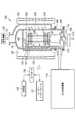
図1に示すように、成膜装置100は、下端が開口された有天井の円筒体状の処理室101を有している。処理室101の全体は、例えば、石英により形成されている。処理室101内の天井には、石英製の天井板102が設けられている。処理室101の下端開口部には、例えば、ステンレススチールにより円筒体状に成形されたマニホールド103がOリング等のシール部材104を介して連結されている。 As shown in FIG. 1, a
マニホールド103は、処理室101の下端を支持している。マニホールド103の下方からは、石英製のウエハボート105が処理室101内に挿入可能となっている。ウエハボート105は、被処理体として複数枚、例えば、50〜100枚の半導体基板、本例では、n型不純物がドープされたn型シリコン基板1を多段に載置可能となっている。これにより、処理室101内には、本例ではn型シリコン基板(ウエハ)1上に、このn型シリコン基板1に達する開孔を有した絶縁膜が形成されている被処理体が収容される。ウエハボート105は複数本の支柱106を有し、支柱106に形成された溝により複数枚のn型シリコン基板1が支持されるようになっている。 The
ウエハボート105は、石英製の保温筒107を介してテーブル108上に載置されている。テーブル108は、マニホールド103の下端開口部を開閉する、例えば、ステンレススチール製の蓋部109を貫通する回転軸110上に支持される。回転軸110の貫通部には、例えば、磁性流体シール111が設けられ、回転軸110を気密にシールしつつ回転可能に支持している。蓋部109の周辺部とマニホールド103の下端部との間には、例えば、Oリングよりなるシール部材112が介設されている。これにより処理室101内のシール性が保持されている。回転軸110は、例えば、ボートエレベータ等の昇降機構(図示せず)に支持されたアーム113の先端に取り付けられている。これにより、ウエハボート105および蓋部109等は、一体的に昇降されて処理室101内に対して挿脱される。 The
成膜装置100は、処理室101内に、処理に使用するガスを供給するガス供給機構114を有している。 The
図2は、図1に示すガス供給機構の一構成例を概略的に示すブロック図である。 FIG. 2 is a block diagram schematically showing a configuration example of the gas supply mechanism shown in FIG.
本例のガス供給機構114は、不活性ガスを供給する不活性ガス供給源115、アミノ基を含まないシラン系ガスを供給するシラン系ガス供給源121、及びアミノシラン系ガスを供給するアミノシラン系ガス供給源122を備えている。本例では、上記ガスの一例として以下のガスが用意、または発生可能に構成されている。 The
不活性ガス: 窒素(N2)ガス
アミノ基を含まないシラン系ガス: モノシラン(SiH4)ガス
アミノシラン系ガス: ジイソプロピルアミノシラン(DIPAS)ガス
ガス供給機構114に備えられたガス供給源は、複数の分散ノズル125に接続される。本例では、シラン系ガス供給源121が流量制御器123f及び開閉弁124fを介して分散ノズル125dに、アミノシラン系ガス供給源122が流量制御器123g及び開閉弁124gを介して分散ノズル125eに接続されている。また、不活性ガス供給源115は、流量制御器123h及び開閉弁126d、126eを介して分散ノズル125d、125eにそれぞれ接続されている。不活性ガスは、アミノ基を含まないシラン系ガス、及びアミノシラン系ガスを希釈する希釈ガス又はキャリアガスに使用、あるいは処理室101の内部をパージするパージガスに使用される。Inert gas: Nitrogen (N2 ) gas
Silane-based gas containing no amino group: Monosilane (SiH4 ) gas
Aminosilane gas: Diisopropylaminosilane (DIPAS) gas
A gas supply source provided in the
なお、不活性ガスをパージガスに使用する場合には、不活性ガス供給源115を、分散ノズル125d、125eとは別に設けられた図示せぬガス導入ポートに接続するようにしてもよい。図示せぬガス導入ポートは、例えば、マニホールド103の側壁を内側に貫通するように設けられる。そして、ガス導入ポートは、分散ノズル125dや125eのガス吐出孔よりも大きなガス吐出孔を有し、マニホールド103の内側を介して処理室101の下方から高さ方向に処理室101内に向けて不活性ガスを供給する。 When an inert gas is used as the purge gas, the inert
複数の分散ノズル125(本例では分散ノズル125d、125e)はそれぞれ、石英管よりなり、マニホールド103の側壁を内側へ貫通して上方向へ屈曲されて、図1に示すように、処理室101の内部に向けて垂直に延びる。なお、図1中では、分散ノズル125の垂直部分には、複数のガス吐出孔127が所定の間隔を隔てて形成されている。上記ガスは、各ガス吐出孔127から水平方向に処理室101内に向けて略均一に吐出される。 Each of the plurality of dispersion nozzles 125 (
処理室101内の、分散ノズル125に対して反対側の部分には、処理室101内を排気するための排気口129が設けられている。排気口129は処理室101の側壁を上下方向へ削りとることによって細長く形成されている。処理室101の排気口129に対応する部分には、排気口129を覆うように断面がコの字状に成形された排気口カバー部材130が溶接により取り付けられている。排気口カバー部材130は、処理室101の側壁に沿って上方に延びており、処理室101の上方にガス出口131を規定している。ガス出口131には、真空ポンプ等を含む排気機構132が接続される。排気機構132は、処理室101内を排気することで処理に使用した処理ガスの排気、及び処理室101内の圧力を処理に応じた処理圧力とする。 An
処理室101の外周には筒体状の加熱装置133が設けられている。加熱装置133は、処理室101内に供給されたガスを活性化するとともに、処理室101内に収容された被処理体、例えば、半導体基板、本例ではn型シリコン基板1を加熱する。 A
成膜装置100の各部の制御は、例えばマイクロプロセッサ(コンピュータ)からなるコントローラ150により行われる。コントローラ150には、オペレータが成膜装置100を管理するためにコマンドの入力操作等を行うキーボードや、成膜装置100の稼働状況を可視化して表示するディスプレイ等からなるユーザーインターフェース151が接続されている。 Control of each part of the
コントローラ150には記憶部152が接続されている。記憶部152は、成膜装置100で実行される各種処理をコントローラ150の制御にて実現するための制御プログラムや、処理条件に応じて成膜装置100の各構成部に処理を実行させるためのプログラムすなわちレシピが格納される。レシピは、例えば、記憶部152の中の記憶媒体に記憶される。記憶媒体は、ハードディスクや半導体メモリであってもよいし、CD-ROM、DVD、フラッシュメモリ等の可搬性のものであってもよい。また、他の装置から、例えば専用回線を介してレシピを適宜伝送させるようにしてもよい。レシピは、必要に応じて、ユーザーインターフェース151からの指示等にて記憶部152から読み出され、読み出されたレシピに従った処理をコントローラ150が実行することで、成膜装置100は、コントローラ150の制御のもと、所望の処理が実施される。本例では、コントローラ150の制御のもと、次に、説明する成膜方法が、一つの処理室101内で順次実行される。 A
図3A〜図3Cは、第1の実施形態に係る成膜装置により実行可能な成膜方法の一例を示す断面図である。 3A to 3C are cross-sectional views illustrating an example of a film forming method that can be executed by the film forming apparatus according to the first embodiment.
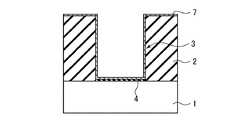
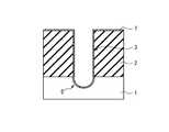
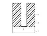
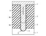
図3Aに示す断面は、n型シリコン基板1上に形成された層間絶縁膜2に、上記n型シリコン基板1に達するコンタクトホール3が形成された時点を示している。 The cross section shown in FIG. 3A shows a point in time when the
図3Aに示すように、コンタクトホール3を形成した後、n型シリコン基板1をエッチング装置の処理室から搬出すると、コンタクトホール3の底に露呈したn型シリコン基板1表面上に、薄い自然酸化膜4が成長する。自然酸化膜4は、コンタクト抵抗を増加させる一因となる。このため、自然酸化膜4は除去されることが良いが、例えば、コンタクトホールの径が大きく、自然酸化膜4によるコンタクト抵抗の増加があったとしても、半導体集積回路装置の動作に支障をきたさない場合には、必ずしも除去する必要はない。本例では、自然酸化膜4を除去しない。 As shown in FIG. 3A, after the
次に、上記自然酸化膜4が成長したn型シリコン基板1を、図1に示した成膜装置100の処理室101内に搬入する。搬入後、加熱装置133を用いて、処理室101内の温度を所定の温度とする。本例では、処理室101内の温度を、例えば、n型シリコン基板1の温度が300℃〜550℃になるような温度とする。 Next, the n-
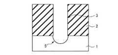
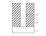
次に、開閉弁124g、及び126eを開け、窒素ガス、及びジイソプロピルアミノシランガス(DIPAS)を、不活性ガス供給源115、及びアミノシラン系ガス供給源122から分散ノズル125eを介して、処理室101内に供給する。この処理により、図3Bに示すように、層間絶縁膜2の表面、及びコンタクトホールの底の表面にシード層7が形成される。処理が終了したら、開閉弁124gを閉じてジイソプロピルアミノシランガスの供給を止めるとともに、処理室101内の雰囲気を窒素ガスにてパージする。この後、排気機構132を停止させるとともに、開閉弁126eを閉じ、窒素ガスの供給を止める。 Next, the on-off
次に、処理室101内の温度を、例えば、n型シリコン基板1の温度が400℃〜650℃になるような温度とする。次いで、開閉弁124f、及び126dを開け、窒素ガス、及びモノシランガス(SiH4)を、不活性ガス供給源115、及びシラン系ガス供給源121から分散ノズル125dを介して、処理室101内に供給する。この処理により、図3Cに示すように、シード層7上にシリコン膜、本例ではアモルファスシリコン膜8aが形成され、コンタクトホール3が埋め込まれる。処理が終了したら、開閉弁124fを閉じてモノシランガスの供給を止めるとともに、処理室101内の雰囲気を窒素ガスにてパージする。この後、排気機構132を停止させるとともに、開閉弁126dを閉じ、窒素ガスの供給を止める。Next, the temperature in the
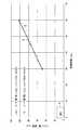
図4に、堆積時間とアモルファスシリコン膜8aの膜厚との関係を示す。図4に示す結果は下地をシリコン酸化膜(SiO2)とした場合である。この下地は、本例では層間絶縁膜2に相当する。FIG. 4 shows the relationship between the deposition time and the thickness of the
本例で用いた処理条件は、
DIPAS流量: 500sccm
処 理 時 間: 5min
処 理 温 度: 400℃
処 理 圧 力: 53.2Pa(0.4Torr)
である。The processing conditions used in this example are:
DIPAS flow rate: 500sccm
Processing time: 5 min
Processing temperature: 400 ℃
Processing pressure: 53.2 Pa (0.4 Torr)
It is.
同じく本例で用いたアモルファスシリコン膜8aを成膜するための処理条件は、
モノシラン流量: 500sccm
堆 積 時 間: 30min/45min/60min
処 理 温 度: 500℃
処 理 圧 力: 53.2Pa(0.4Torr)
である。Similarly, the processing conditions for forming the
Monosilane flow rate: 500sccm
Deposition time: 30min / 45min / 60min
Processing temperature: 500 ℃
Processing pressure: 53.2 Pa (0.4 Torr)
It is.
アモルファスシリコン膜8aの膜厚は、堆積時間を30minとしたとき、45minとしたとき、及び60minとしたときの3点で測定した。 The film thickness of the
図4中の線Iはシード層7有りの場合、線IIはシード層7無しの場合の結果を示している。線I、IIは、測定された3つの膜厚を最小二乗法で直線近似した直線であり、式は次の通りである。 The line I in FIG. 4 indicates the result when the
線I : y = 17.572x − 20.855 …(1)
線II : y = 17.605x − 34.929 …(2)
図4に示すように、シード層7有りの場合、シード層7無しに比較してアモルファスシリコン膜8aの膜厚が増す傾向が明らかとなった。Line I: y = 17.572x-20.855 (1)
Line II: y = 17.605x-34.929 (2)
As shown in FIG. 4, when the
上記(1)、(2)式をy=0、即ち、アモルファスシリコン膜8aの膜厚を“0”としたとき、線I、IIと堆積時間との交点を求めたものを図5に示す。 FIG. 5 shows the intersections of the lines I and II and the deposition time when the above equations (1) and (2) are set to y = 0, that is, the film thickness of the
なお、図5は図4中の破線枠A内を拡大した拡大図である。 FIG. 5 is an enlarged view of the inside of the broken line frame A in FIG.
図5に示すように、下地がシード層7有りのシリコン酸化膜のとき、アモルファスシリコン膜8aの堆積が処理開始から約1.2min(x≒1.189)から始まる。対して、下地がシード層7無しのシリコン酸化膜のときには、アモルファスシリコン膜8aの堆積が処理開始から約2.0min(x≒1.984)から始まる。 As shown in FIG. 5, when the base is a silicon oxide film with the
このように、下地に対してアミノシラン系ガスを用いてシード層7を形成することで、インキュベーション時間を、約2.0minから約1.2minに短縮することができる。 In this way, by forming the
このような第1の実施形態に係る成膜装置100によれば、コンタクトホール3の埋め込み工程を、アミノシラン系ガスを用いてシード層7を層間絶縁膜2の表面、及びコンタクトホールの底の表面に形成してから、アミノ基を含まないシラン系ガスを用いてシリコン膜、本例ではアモルファスシリコン膜8aをシード層7上に形成する。これらの工程を実施できることにより、シード層7を形成しない場合に比較してアモルファスシリコン膜8aのインキュベーション時間を短縮することができる。 According to the
このように、コンタクトホール3を埋め込むアモルファスシリコン膜8aのインキュベーション時間を短縮することができる結果、埋め込み工程におけるスループットを向上でき、埋め込み工程が多用される半導体集積回路装置であっても、優れた生産能力を発揮することが可能な成膜装置100が得られる、という利点を得ることができる。 As described above, the incubation time of the
(変形例)
図6A〜図6Cは、第1の実施形態に係る成膜装置により実行可能な成膜方法の変形例を示す断面図である。(Modification)
6A to 6C are cross-sectional views illustrating modifications of the film forming method that can be executed by the film forming apparatus according to the first embodiment.
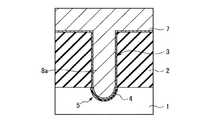
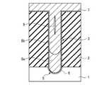
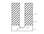
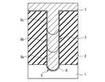
コンタクトホール3の微細化が進み、図6Aに示すように、コンタクトホール3の径が狭くなり、コンタクト部の表面積が小さくなると、コンタクト抵抗が増加する、という事情がある。このようなコンタクト抵抗の増加の解消策の一つとして、図6A中の参照符号5により示すように、コンタクトホール3の底を掘り下げ、コンタクト部の表面積を増加させる、という手法がある。 As the
第1の実施形態は、コンタクトホール3の底を掘り下げておいた半導体集積回路装置であっても、図6A〜図6Cに示すように適用することが可能である。 The first embodiment can be applied to a semiconductor integrated circuit device in which the bottom of the
なお、第1の実施形態の一例と本変形例との相違点は、コンタクトホール3の底を掘り下げているか否かであり、製法については図3A〜図3Cに示した一例と同様である。よって、変形例の説明は、図6A〜図6Cへの図示のみとして割愛する。 The difference between the example of the first embodiment and this modification is whether or not the bottom of the
また、以下に説明する実施形態は、コンタクトホール3の底を掘り下げた例に従って説明することとする。 Further, the embodiment described below will be described according to an example in which the bottom of the
(第2の実施形態)
図7は、この発明の第2の実施形態に係る成膜装置が備えるガス供給機構の一構成例を概略的に示すブロック図である。(Second Embodiment)
FIG. 7 is a block diagram schematically showing a configuration example of the gas supply mechanism provided in the film forming apparatus according to the second embodiment of the present invention.
図7に示すように、第2の実施形態に係る成膜装置が備えるガス供給機構114が、第1の実施形態に係る成膜装置のガス供給機構114と異なるところは、自然酸化膜を除去することが可能なガスを供給するガス供給源を、さらに備えていることである。 As shown in FIG. 7, the
本例では、自然酸化膜を除去することが可能なガスとして二つのガスを利用し、自然酸化膜を除去可能な第1のガスを供給する第1のガス供給源116、同じく自然酸化膜を除去可能な上記第1のガスと異なる第2のガスを供給する第2のガス供給源117を備える。 In this example, two gases are used as the gas capable of removing the natural oxide film, the first
本例では、上記ガスの一例として以下のガスが用意、または発生可能に構成されている。 In this example, the following gas is prepared or generated as an example of the gas.
第1のガス: アンモニア(NH3)ガス
第2のガス: フッ化水素(HF)ガス
第1のガス供給源116は、流量制御器123a及び開閉弁124aを介して、分散ノズル125aに接続されている。同様に、第2のガス供給源117は流量制御器123b及び開閉弁124bを介して分散ノズル125bに接続されている。First gas: Ammonia (NH3 ) gas
Second gas: Hydrogen fluoride (HF) gas
The first
分散ノズル125a、125bはそれぞれ、他の分散ノズルと同様に石英管よりなり、マニホールド103の側壁を内側へ貫通して上方向へ屈曲されて、図1に示したように、処理室101の内部に向けて垂直に延びる。 Each of the
図8A〜図8Dは、第2の実施形態に係る成膜装置により実行可能な成膜方法の一例を示す断面図である。 8A to 8D are cross-sectional views illustrating an example of a film forming method that can be executed by the film forming apparatus according to the second embodiment.
まず、図8Aに示すように、上記自然酸化膜4が成長したn型シリコン基板1を、成膜装置100の処理室101内に搬入する。搬入後、加熱装置133を用いて、処理室101内の温度を所定の温度とする。本例では処理室101内の温度を、n型シリコン基板1の温度が20℃〜300℃になるような温度とした。次いで、図7に示す開閉弁124a、124b、126a、及び126bを開け、窒素ガス(N2)、アンモニアガス(NH3)、及びフッ化水素ガス(HF)を、それぞれ不活性ガス供給源115、第1のガス供給源116、及び第2のガス供給源117から分散ノズル125a、及び125bを介して、処理室101内に供給する。この処理により、図8Bに示すように、コンタクトホール3の底に露呈したn型シリコン基板1表面上の自然酸化膜4が除去される。処理が終了したら、開閉弁124a、及び124bを閉じ、アンモニアガス、及びフッ化水素ガスの供給を止める。これとともに、排気機構132を用いて、処理室101内を排気しながら、窒素ガスを処理室101内に供給し、処理室101内の雰囲気を窒素ガスにてパージする。この後、排気機構132を停止させるとともに、開閉弁126a、及び126bを閉じ、窒素ガスの供給を止める。First, as shown in FIG. 8A, the n-
この後、図8C、図8Dに示すように、上記図3B、図3Cを参照して説明した製法に従って、シード層7、及びアモルファスシリコン膜8aを形成する。 Thereafter, as shown in FIGS. 8C and 8D, the
このような第2の実施形態に係る成膜装置によれば、コンタクトホール3の埋め込み工程を第1の実施形態と同様に行うので、コンタクトホール3を埋め込むアモルファスシリコン膜8aのインキュベーション時間を短縮でき、埋め込み工程におけるスループットを向上できる。よって、第1の実施形態と同様に、埋め込み工程が多用される半導体集積回路装置であっても、優れた生産能力を発揮することが可能な成膜装置100が得られる、という利点を得ることができる。 According to the film forming apparatus according to the second embodiment, since the step of filling the
上記利点に、さらに加え、第2の実施形態に係る成膜装置によれば、自然酸化膜4を除去することができるので、コンタクト抵抗の増加を抑制することができる、という利点を得ることができる。 In addition to the above advantages, according to the film forming apparatus according to the second embodiment, the
しかも、自然酸化膜4の除去は、アモルファスシリコン膜8aの成膜を行う成膜装置の処理室内で行われる。このため、自然酸化膜4を除去した後、すみやかにアモルファスシリコン膜8aの成膜を行える。このため、自然酸化膜4の除去を行う場合において、埋め込み工程におけるスループットの悪化を抑制できる、という利点も得ることができる。 Moreover, the removal of the
(第3の実施形態)
図9は、この発明の第3の実施形態に係る成膜装置が備えるガス供給機構の一構成例を概略的に示すブロック図である。(Third embodiment)
FIG. 9 is a block diagram schematically showing a configuration example of the gas supply mechanism provided in the film forming apparatus according to the third embodiment of the present invention.
図9に示すように、第3の実施形態に係る成膜装置が備えるガス供給機構114が、第2の実施形態に係る成膜装置のガス供給機構114と異なるところは、ドーパントを含むガスを供給するドーパントガス供給源120を、さらに備えていることである。 As shown in FIG. 9, the
本例では、ドーパントして、n型シリコン基板1の導電型と同じn型不純物を選んでいる。ドーパントガス供給源120は、n型不純物を含むガスとして以下のガスが用意、または発生可能に構成されている。 In this example, the same n-type impurity as the conductivity type of the n-
ドーパントガス: ホスフィン(PH3)ガス
本例のドーパントガス供給源120は、流量制御器123e及び開閉弁124eを介して分散ノズル125dに接続されている。Dopant gas: Phosphine (PH3 ) gas The dopant
図10A〜図10Cは、第3の実施形態に係る成膜装置により実行可能な成膜方法の一例を示す断面図である。 10A to 10C are cross-sectional views illustrating an example of a film forming method that can be executed by the film forming apparatus according to the third embodiment.
例えば、第2の実施形態で説明した製法に従って、コンタクトホール3の底に露呈したn型シリコン基板1表面上の自然酸化膜4を除去する。この後、処理室101内の温度を、例えば、n型シリコン基板1の温度が400℃〜650℃になるような温度とする。次いで、開閉弁124e、及び126dを開け、窒素ガス、及びホスフィンガス(PH3)を、不活性ガス供給源115、及びドーパントガス供給源120から分散ノズル125dを介して、処理室101内に供給する。For example, the
この処理により、図10Aに示すように、掘り下げられたn型シリコン基板1の表面にn型不純物であるリン(P)が参照符号6に示すように吸着され、n型シリコン基板1の表面部分のn型不純物濃度が高まる。この結果、n型シリコン基板1の表面部分の抵抗値が下がる。処理が終了したら、開閉弁124eを閉じてホスフィンガスの供給を止めるとともに、処理室101内の雰囲気を窒素ガスにてパージする。この後、排気機構132を停止させるとともに、開閉弁126dを閉じ、窒素ガスの供給を止める。 By this process, as shown in FIG. 10A, phosphorus (P), which is an n-type impurity, is adsorbed on the surface of the n-
この後、図10B、図10Cに示すように、上記図3B、図3Cを参照して説明した製法に従って、シード層7、及びアモルファスシリコン膜8aを形成する。 Thereafter, as shown in FIGS. 10B and 10C, the
このような第3の実施形態に係る成膜装置においても、コンタクトホール3の埋め込み工程を第1の実施形態と同様に行う。このため、第1の実施形態と同様に、埋め込み工程が多用される半導体集積回路装置であっても、優れた生産能力を発揮することが可能な成膜装置100が得られる、という利点を得ることができる。 Also in the film forming apparatus according to the third embodiment, the process of filling the
さらに、第3の実施形態に係る成膜装置によれば、n型不純物をコンタクトホール3の底のn型シリコン基板1の表面部分に導入することができる。このため、コンタクトホール3の底のn型シリコン基板1のn型不純物濃度を高めることができ、コンタクト抵抗を低下させることができる、という利点を得ることができる。 Furthermore, according to the film forming apparatus of the third embodiment, n-type impurities can be introduced into the surface portion of the n-
しかも、n型不純物の導入はアモルファスシリコン膜8aを成膜する成膜装置の処理室内で行われる。よって、n型不純物を導入した後、すみやかにアモルファスシリコン膜8aの成膜を行える。このため、n型不純物の導入を行う場合において、埋め込み工程におけるスループットの悪化を抑制できる、という利点も得ることができる。 Moreover, the introduction of the n-type impurity is performed in the processing chamber of the film forming apparatus for forming the
(変形例)
図11A〜図11Cは、第3の実施形態に係る成膜装置により実行可能な成膜方法の変形例を示す断面図である。(Modification)
11A to 11C are cross-sectional views illustrating modifications of the film forming method that can be executed by the film forming apparatus according to the third embodiment.
上記第3の実施形態では、n型不純物をn型シリコン基板1に導入したが、第3の実施形態に係る成膜装置は、n型不純物をアモルファスシリコン膜8aに導入することも可能である。 In the third embodiment, the n-type impurity is introduced into the n-
図11A、図11Bに示すように、図8B、図8Cを参照して説明した製法に従って、シード層7を形成した後、開閉弁124e、126d、124fを開け、窒素ガス、ホスフィンガス、及びモノシランガスを、不活性ガス供給源115、ドーパントガス供給源120、及びシラン系ガス供給源121から分散ノズル125dを介して、処理室101内に供給する。このような処理により、図11Cに示すように、n型不純物、本例ではリン(P)を含有したドープトアモルファスシリコン膜8a*が形成され、コンタクトホール3は、ドープトアモルファスシリコン膜8a*によって埋め込まれる。また、n型シリコン基板1のn型不純物濃度よりも、ドープトアモルファスシリコン膜8a*のn型不純物濃度が高い場合には、図11Cに示すように、例えば、ドープトアモルファスシリコン膜8a*からn型シリコン基板1に向かってn型不純物が拡散する。As shown in FIGS. 11A and 11B, after forming the
このように、n型不純物をアモルファスシリコン膜8aに導入し、ドープトアモルファスシリコン膜8a*とすることも可能である。この場合においても、ドープトアモルファスシリコン膜8a*は抵抗が小さくなる結果、コンタクト抵抗を低下させることができる、という利点を得ることができる。As described above, it is possible to introduce the n-type impurity into the
また、n型シリコン基板1のn型不純物濃度よりも、ドープトアモルファスシリコン膜8a*のn型不純物濃度が高い場合には、図11Cに示すように、例えば、ドープトアモルファスシリコン膜8a*からn型シリコン基板1に向かってn型不純物が拡散する。この拡散を利用することで、n型シリコン基板1のコンタクト部分の抵抗についても小さくすることが可能できる。In addition, when the n-type impurity concentration of the doped
もちろん、n型シリコン基板1のコンタクト部分には、図10Aを参照して説明したようにn型不純物を導入しておき、さらに、図11Cを参照して説明した製法に従ってドープトアモルファスシリコン膜8a*を形成するようにしても良い。Of course, an n-type impurity is introduced into the contact portion of the n-
(第4の実施形態)
図12は、この発明の第4の実施形態に係る成膜装置が備えるガス供給機構の一構成例を概略的に示すブロック図である。(Fourth embodiment)
FIG. 12 is a block diagram schematically showing a configuration example of the gas supply mechanism provided in the film forming apparatus according to the fourth embodiment of the present invention.
図12に示すように、第4の実施形態に係る成膜装置が備えるガス供給機構114が、第3の実施形態に係る成膜装置のガス供給機構114と異なるところは、シリコンをエッチング可能なガスを供給する第3のガス供給源119を、さらに備えていることである。 As shown in FIG. 12, the
本例では、第3のガス供給源119は、シリコンをエッチング可能なガスとして以下のガスが用意、または発生可能に構成されている。 In this example, the third
シリコンをエッチング可能なガス: 塩素(Cl2)ガス
本例の第3のガス供給源119は、流量制御器123d及び開閉弁124dを介して分散ノズル125cに接続されている。Gas capable of etching silicon: Chlorine (Cl2 ) gas The third
分散ノズル125cもまた、石英管よりなり、マニホールド103の側壁を内側へ貫通して上方向へ屈曲されて、図1に示すように、処理室101の内部に向けて垂直に延びる。 The
図13A〜図13Eは、第4の実施形態に係る成膜装置により実行可能な成膜方法の一例を示す断面図である。 13A to 13E are cross-sectional views illustrating an example of a film forming method that can be executed by the film forming apparatus according to the fourth embodiment.
アモルファスシリコン膜8aを形成した段階で、コンタクトホール3の埋め込みを終了させることも可能である。しかし、コンタクトホール3のアスペクト比が高い(コンタクトホール3が高さ方向に細長い)場合には、図13Aに示すように、アモルファスシリコン膜8aにボイド9が生じることがある。本例では、ボイド9が生じていることを想定して、さらに、以下の処理を実行する。 It is also possible to end the filling of the
まず、処理室101内の温度を、例えば、n型シリコン基板1の温度が200℃〜500℃になるような温度とする。次いで、開閉弁124d、及び126cを開け、窒素ガス、及び塩素ガス(Cl2)を、不活性ガス供給源115、及び第3のガス供給源119から分散ノズル125cを介して、処理室101内に供給する。この処理により、図13Bに示すように、アモルファスシリコン膜8aがコンタクトホール3の途中まで、例えば、アモルファスシリコン膜8aにおいてボイド9が生じている、と想定される領域が除去される。処理が終了したら、開閉弁124dを閉じて塩素ガスの供給を止めるとともに、処理室101内の雰囲気を窒素ガスにてパージする。この後、排気機構132を停止させるとともに、開閉弁126cを閉じ、窒素ガスの供給を止める。First, the temperature in the
次に、処理室101内の温度を、例えば、n型シリコン基板1の温度が400℃〜650℃になるような温度とする。次いで、開閉弁124f、及び126dを開け、窒素ガス、及びモノシランガス(SiH4)を、不活性ガス供給源115、及びシラン系ガス供給源121から分散ノズル125dを介して、処理室101内に供給する。この処理により、図13Cに示すように、シード層7上及びアモルファスシリコン膜8a上にシリコン膜、本例ではアモルファスシリコン膜8bが形成され、コンタクトホール3が再度埋め込まれる。処理が終了したら、開閉弁124fを閉じてモノシランガスの供給を止めるとともに、処理室101内の雰囲気を窒素ガスにてパージする。この後、排気機構132を停止させるとともに、開閉弁126dを閉じ、窒素ガスの供給を止める。Next, the temperature in the
このような堆積、エッチングを、例えば、図13D、図13Eに示すように繰り返し、アモルファスシリコン膜8a、8bから、ボイド9が生じている、と想定される領域を除去しながら、コンタクトホール3を、アモルファスシリコン膜8a、8b、及び8cにより埋め込んでいく。最後のアモルファスシリコン膜、本例では第3層目アモルファスシリコン膜8cの形成が終了したら、n型シリコン基板1を処理室101内から搬出する。 Such deposition and etching are repeated as shown in FIGS. 13D and 13E, for example, and the
このような第4の実施形態に係る成膜装置においても、コンタクトホール3の埋め込み工程の最初の段階、即ちアモルファスシリコン膜8aの形成を第1の実施形態と同様に行う。このため、第1の実施形態と同様の利点を得ることができる。 In the film forming apparatus according to the fourth embodiment, the first step of the
また、第4の実施形態に係る成膜装置によれば、アモルファスシリコン膜8a、8bに生じているボイド9を除去することができるので、ボイドが発生することによって抵抗が高くなってしまう事情を解消することができる。 In addition, according to the film forming apparatus according to the fourth embodiment, the
また、アモルファスシリコン膜8a、8bの成膜とエッチングとを同じ成膜装置の処理室内で行うことができるので、成膜工程とエッチング工程とで装置間での搬送作業の必要がなく、スループットの低下を抑制することができる、という利点も得ることができる。 In addition, since the
(第5の実施形態)
上記第1の実施形態は成膜される膜のインキュベーション時間を短くし、埋め込み工程におけるスループット向上を主眼とした例であった。(Fifth embodiment)
The first embodiment is an example in which the incubation time of the film to be formed is shortened and the throughput is increased in the embedding process.
また、第2〜第4の実施形態はスループット向上とともに、微細化が進んだコンタクトホールやラインにおいてはコンタクト抵抗が増加する、という事情の解消を図った例であった。微細化が進んだコンタクトホールやラインにおいて、コンタクト抵抗が増加する原因としては、第2〜第4の実施形態で説明したように、例えば、
1)自然酸化膜による抵抗増加の影響が顕著化すること
2)コンタクト部の表面積が小さくなること
3)埋め込まれる導電物の体積が小さく、導電物に発生するボイドによる体積減が大きく現われること
などが挙げられる。Further, the second to fourth embodiments are examples in which the situation that the contact resistance increases in contact holes and lines that have been miniaturized as the throughput is improved is solved. As described in the second to fourth embodiments, the reason why the contact resistance increases in the contact holes and lines that have been miniaturized is, for example,
1) The effect of increased resistance due to the natural oxide film becomes prominent 2) The surface area of the contact portion becomes smaller 3) The volume of the embedded conductive material is small, and the volume decrease due to voids generated in the conductive material appears greatly Is mentioned.
第5の実施形態は、1)〜3)の事情を一台の成膜装置で解決でき、かつ、成膜される膜のインキュベーション時間も短く、スループットの向上も図ることができる成膜装置を提供しようとする例である。 In the fifth embodiment, there is provided a film forming apparatus that can solve the problems 1) to 3) with a single film forming apparatus, has a short incubation time of the film to be formed, and can improve the throughput. This is an example to be provided.
図14は、この発明の第5の実施形態に係る成膜装置が備えるガス供給機構の一構成例を概略的に示すブロック図である。 FIG. 14 is a block diagram schematically showing a configuration example of a gas supply mechanism provided in a film forming apparatus according to the fifth embodiment of the present invention.
図14に示すように、第5の実施形態に係る成膜装置が備えるガス供給機構114が、第4の実施形態に係る成膜装置のガス供給機構114と異なるところは、導電体、本例ではn型シリコン基板1をエッチング可能な第4のガスを供給する第4のガス供給源118を、さらに備えていることである。 As shown in FIG. 14, the
本例では、第4のガス供給源118は、導電体をエッチング可能なガスとして以下のガスが用意、または発生可能に構成されている。 In this example, the fourth
導電体をエッチング可能なガス: フッ素(F2)ガス
本例の第4のガス供給源118は、流量制御器123c及び開閉弁124cを介して分散ノズル125cに接続されている。Gas capable of etching the conductor: Fluorine (F2 ) gas The fourth
図15は、第5の実施形態に係る成膜装置により実行可能な成膜方法の処理ガス供給及び処理温度の一例を示すタイムチャート、また、図16A〜図16Jは、その成膜方法の一例を示す断面図である。 FIG. 15 is a time chart showing an example of processing gas supply and processing temperature of a film forming method that can be executed by the film forming apparatus according to the fifth embodiment, and FIGS. 16A to 16J are examples of the film forming method. FIG.
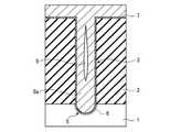
まず、図16Aに示す断面は、n型シリコン基板1上に形成された層間絶縁膜2に、上記n型シリコン基板1に達するコンタクトホール3が形成された時点を示している。 First, the cross section shown in FIG. 16A shows a point in time when the
図16Aに示すように、コンタクトホール3を形成した後、n型シリコン基板1をエッチング装置の処理室から搬出すると、コンタクトホール3の底に露呈したn型シリコン基板1表面上に、薄い自然酸化膜4が成長する。 As shown in FIG. 16A, when the n-
次に、上記自然酸化膜4が成長したn型シリコン基板1を、図1に示した成膜装置100の処理室101内に搬入する。搬入後、加熱装置133を用いて、処理室101内の温度を所定の温度とする。本例では処理室101内の温度を、n型シリコン基板1の温度が20℃〜300℃になるような温度とした。次いで、図14に示す開閉弁124a、124b、126a、及び126bを開け、窒素ガス(N2)、アンモニアガス(NH3)、及びフッ化水素ガス(HF)を、それぞれ不活性ガス供給源115、第1のガス供給源116、及び第2のガス供給源117から分散ノズル125a、及び125bを介して、処理室101内に供給する(図15中のステップ1:COR)。この処理により、図16Bに示すように、コンタクトホール3の底に露呈したn型シリコン基板1表面上の自然酸化膜4が除去される。処理が終了したら、開閉弁124a、及び124bを閉じ、アンモニアガス、及びフッ化水素ガスの供給を止める。これとともに、排気機構132を用いて、処理室101内を排気しながら、窒素ガスを処理室101内に供給し、処理室101内の雰囲気を窒素ガスにてパージする。この後、排気機構132を停止させるとともに、開閉弁126a、及び126bを閉じ、窒素ガスの供給を止める。Next, the n-
次に、第2の実施形態と同様に、処理室101内の温度を、例えば、n型シリコン基板1の温度が20℃〜300℃になるような温度とする。次いで、開閉弁124c、及び126cを開け、窒素ガス、及びフッ素ガス(F2)を、不活性ガス供給源115、及び第4のガス供給源118から分散ノズル125cを介して、処理室101内に供給する(図15中のステップ2:Si recess)。この処理により、図16Cに示すように、コンタクトホール3の底に露呈したn型シリコン基板1が参照符号5に示すように掘り下げられる。処理が終了したら、開閉弁124cを閉じてフッ素ガスの供給を止めるとともに、処理室101内の雰囲気を窒素ガスにてパージする。この後、排気機構132を停止させるとともに、開閉弁126cを閉じ、窒素ガスの供給を止める。Next, as in the second embodiment, the temperature in the
次に、第3の実施形態と同様に、処理室101内の温度を、例えば、n型シリコン基板1の温度が400℃〜650℃になるような温度とする。次いで、開閉弁124e、及び126dを開け、窒素ガス、及びホスフィンガス(PH3)を、不活性ガス供給源115、及びドーパントガス供給源120から分散ノズル125dを介して、処理室101内に供給する(図15中のステップ3:PH3 adsorption)。この処理により、図16Dに示すように、掘り下げられたn型シリコン基板1の表面にn型不純物であるリン(P)が参照符号6に示すように吸着され、n型シリコン基板1の表面部分のn型不純物濃度が高まる。この結果、n型シリコン基板1の表面部分の抵抗値が下がる。処理が終了したら、開閉弁124eを閉じてホスフィンガスの供給を止めるとともに、処理室101内の雰囲気を窒素ガスにてパージする。この後、排気機構132を停止させるとともに、開閉弁126dを閉じ、窒素ガスの供給を止める。Next, as in the third embodiment, the temperature in the
次に、第1の実施形態と同様に、処理室101内の温度を、例えば、n型シリコン基板1の温度が300℃〜550℃になるような温度とする。次いで、開閉弁124g、及び126eを開け、窒素ガス、及びジイソプロピルアミノシランガス(DIPAS、図15中ではPre−Xと表記)を、不活性ガス供給源115、及びアミノシラン系ガス供給源122から分散ノズル125eを介して、処理室101内に供給する(図15中のステップ4:Seed)。この処理により、図16Eに示すように、層間絶縁膜2、及び掘り下げられたn型シリコン基板1の表面にシード層7が形成される。処理が終了したら、開閉弁124gを閉じてジイソプロピルアミノシランガスの供給を止めるとともに、処理室101内の雰囲気を窒素ガスにてパージする。この後、排気機構132を停止させるとともに、開閉弁126eを閉じ、窒素ガスの供給を止める。 Next, as in the first embodiment, the temperature in the
次に、処理室101内の温度を、例えば、n型シリコン基板1の温度が400℃〜650℃になるような温度とする。次いで、開閉弁124f、及び126dを開け、窒素ガス、及びモノシランガス(SiH4)を、不活性ガス供給源115、及びシラン系ガス供給源121から分散ノズル125dを介して、処理室101内に供給する(図15中のステップ5:Depo)。この処理により、図16Fに示すように、シード層7上にシリコン膜、本例ではアモルファスシリコン膜8aが形成され、コンタクトホール3が埋め込まれる。処理が終了したら、開閉弁124fを閉じてモノシランガスの供給を止めるとともに、処理室101内の雰囲気を窒素ガスにてパージする。この後、排気機構132を停止させるとともに、開閉弁126dを閉じ、窒素ガスの供給を止める。Next, the temperature in the
なお、本例においても、ドーパントガス供給源120から分散ノズル125dを介してアモルファスシリコン膜8aにドーパントを導入し、第3の実施形態の変形例と同様に、ドープトアモルファスシリコン膜8a*とすることも可能である。Also in this example, a dopant is introduced into the
また、本例においても、アモルファスシリコン膜8aを形成した段階で、コンタクトホール3の埋め込みを終了させることも可能である。しかし、第4の実施形態のように、エッチングと成膜を繰り返し、アモルファスシリコン膜8aからボイド9を除去しながら、成膜することも可能である。本例では、ボイド9が生じていることを想定して、さらに、以下の処理を実行する。 Also in this example, the filling of the
第4の実施形態と同様に、処理室101内の温度を、例えば、n型シリコン基板1の温度が200℃〜500℃になるような温度とする。次いで、開閉弁124d、及び126cを開け、窒素ガス、及び塩素ガス(Cl2)を、不活性ガス供給源115、及び第3のガス供給源119から分散ノズル125cを介して、処理室101内に供給する(図15中のステップ6:Etch)。この処理により、図16Gに示すように、アモルファスシリコン膜8aがコンタクトホール8aの途中まで、例えば、アモルファスシリコン膜8aにおいてボイド9が生じている、と想定される領域が除去される。処理が終了したら、開閉弁124dを閉じて塩素ガスの供給を止めるとともに、処理室101内の雰囲気を窒素ガスにてパージする。この後、排気機構132を停止させるとともに、開閉弁126cを閉じ、窒素ガスの供給を止める。Similarly to the fourth embodiment, the temperature in the
次に、処理室101内の温度を、例えば、n型シリコン基板1の温度が400℃〜650℃になるような温度とする。次いで、開閉弁124f、及び126dを開け、窒素ガス、及びモノシランガス(SiH4)を、不活性ガス供給源115、及びシラン系ガス供給源121から分散ノズル125dを介して、処理室101内に供給する(図15中のステップ7:Depo)。この処理により、図16Hに示すように、シード層7上及びアモルファスシリコン膜8a上にシリコン膜、本例ではアモルファスシリコン膜8bが形成され、コンタクトホール3が再度埋め込まれる。処理が終了したら、開閉弁124fを閉じてモノシランガスの供給を止めるとともに、処理室101内の雰囲気を窒素ガスにてパージする。この後、排気機構132を停止させるとともに、開閉弁126dを閉じ、窒素ガスの供給を止める。Next, the temperature in the
このような堆積、エッチングを、例えば、図16I、図16Jに示すように繰り返し、アモルファスシリコン膜8a、8bから、ボイド9が生じている、と想定される領域を除去しながら、コンタクトホール3を、アモルファスシリコン膜8a、8b、及び8cにより埋め込んでいく。最後のアモルファスシリコン膜、本例では第3層目アモルファスシリコン膜8cの形成が終了したら、n型シリコン基板1を処理室101内から搬出する。 Such deposition and etching are repeated, for example, as shown in FIGS. 16I and 16J, and the
なお、アモルファスシリコン膜8b、及び8cにおいても、第3の実施形態の変形例と同様に、ドープトアモルファスシリコン膜としても良い。 Note that the
このようにして第5の実施形態に係る成膜装置を用いた成膜方法、本例ではコンタクトホール3の埋め込みプロセスが終了する。 Thus, the film forming method using the film forming apparatus according to the fifth embodiment, in this example, the process of filling the
このような第5の実施形態に係る成膜装置によれば、たとえ、コンタクトホールの微細化が進んだ、としても、
(1) ステップ1において、コンタクトホール3の底に露呈したn型シリコン基板1表面上から自然酸化膜4が除去される。このため、自然酸化膜4によるコンタクト抵抗増加を抑制できる、
(2) ステップ2において、コンタクトホール3の底に露呈したn型シリコン基板1が掘り下げられる。このため、コンタクト部の表面積を、掘り下げない場合に比較して大きくすることができ、コンタクト部の表面積が小さくなることによるコンタクト抵抗増加を抑制できる、
(3) 上記(1)、(2)の利点を維持したまま、ステップ4において、アミノシラン系ガスを用いてシード層7を形成する。このため、ステップ5におけるシラン系ガスを用いて形成されるアモルファスシリコン膜8aのインキュベーション時間を短縮できる、という利点を得ることができる。According to the film forming apparatus according to the fifth embodiment, even if the contact hole has been miniaturized,
(1) In
(2) In
(3) While maintaining the advantages (1) and (2) above, in
しかも、上記(1)〜(3)の利点を、一台の成膜装置100による処理だけで得ることができる。 Moreover, the advantages (1) to (3) can be obtained only by the processing by one
また、上記第5の実施形態においては、
(4) ステップ6、7において、アモルファスシリコン膜の堆積、及びエッチングを繰り返すことで、堆積されたアモルファスシリコン膜中に発生するであろうボイドが除去される。このため、コンタクトホール3内に埋め込まれたアモルファスシリコン膜の、ボイドによる体積減を抑制でき、体積減によるコンタクト抵抗増加を抑制できる、という利点も得ることができる。In the fifth embodiment,
(4) By repeating the deposition and etching of the amorphous silicon film in
さらに、上記第5の実施形態においては、
(5) ステップ3において、掘り下げられたn型シリコン基板1の表面にn型不純物であるリン(P)を吸着させる。このため、n型シリコン基板1の表面部分のn型不純物濃度を高めることができ、n型シリコン基板1の表面部分の抵抗値を下げることができる、という利点についても得ることができる。Furthermore, in the fifth embodiment,
(5) In
これら(4)、(5)の利点についても、(1)〜(3)の利点と同時に、一台の成膜装置100による処理だけで得ることが可能である。 The advantages (4) and (5) can be obtained only by the processing by the single
したがって、第5の実施形態に係る成膜装置によれば、微細化が進んだコンタクトホールにおいても、コンタクト抵抗の増加を抑制、または減少できる成膜が可能であり、かつ、成膜される膜のインキュベーション時間も短く、スループットの向上も図ることができる成膜装置を提供できる。 Therefore, according to the film forming apparatus according to the fifth embodiment, it is possible to form a film capable of suppressing or reducing an increase in contact resistance even in a contact hole that has been miniaturized, and a film to be formed It is possible to provide a film forming apparatus that can shorten the incubation time and improve the throughput.
以上、この発明を第1〜第5の実施形態に従って説明したが、この発明は上記第1〜第5の実施形態に限定されることは無く、種々変形可能である。 As mentioned above, although this invention was demonstrated according to the 1st-5th embodiment, this invention is not limited to the said 1st-5th embodiment, A various deformation | transformation is possible.
例えば、上記第5の実施形態においては、ステップ6でアモルファスシリコン膜8aをエッチングした後に続いて、ステップ7においてアミノ基を含まないシラン系ガスを用いてアモルファスシリコン膜8bを形成した。 For example, in the fifth embodiment, after the
しかし、アモルファスシリコン膜8aをコンタクトホール3の途中まで除去した後、処理室101内にアミノシラン系ガスを再度供給し、層間絶縁膜2、及びアモルファスシリコン膜8a表面に新たなシード層を形成し、この後、処理室101内にアミノ基を含まないシラン系ガスを再度供給し、新たなシード層上に新たなアモルファスシリコン膜8bを形成するようにすることも可能である。 However, after the
また、上記第5の実施形態においては、成膜装置100を、n型シリコン基板1に達するコンタクトホール3内の埋め込みプロセスに適用した例を説明した。 In the fifth embodiment, the example in which the
しかし、コンタクトホール3内の埋め込みプロセスに限らず、凹状のラインの埋め込みプロセスにも、上記利点をもって適用することができる。 However, the present invention can be applied not only to the process of filling the
また、コンタクトホール3にあっては、n型シリコン基板1に達するものばかりでなく、p型シリコン基板であっても良いし、n型又はp型のシリコン基板、又はウェルに形成されたソース領域やドレイン領域のような活性領域に達するものであっても良い。また、半導体領域ばかりでなく、銅などのメタル配線に達するものであっても良い。メタル配線のように半導体領域以外に達する場合には、図15に示したステップ3、いわゆるドーパントの吸着工程は省略することができる。 Further, the
また、上記第1〜第5の実施形態においては、アミノシラン系ガスとして、ジイソプロピルアミノシランガス(DIPAS)を用いたが、アミノシラン系ガスとしては、DIPASの他、下記のアミノシラン系ガスを使うことができる。 In the first to fifth embodiments, diisopropylaminosilane gas (DIPAS) is used as the aminosilane-based gas. As aminosilane-based gas, the following aminosilane-based gas can be used in addition to DIPAS. .
BAS(ブチルアミノシラン)
BTBAS(ビスターシャリブチルアミノシラン)
DMAS(ジメチルアミノシラン)
BDMAS(ビスジメチルアミノシラン)
TDMAS(トリジメチルアミノシラン)
DEAS(ジエチルアミノシラン)
BDEAS(ビスジエチルアミノシラン)、及び
DPAS(ジプロピルアミノシラン)
また、上記一実施形態においては、アミノ基を含まないシラン系ガスとして、モノシランガス(SiH4)を用いたが、アミノシラン系ガスとしては、SiH4の他、下記のアミノ基を含まないシラン系ガスを使うことができる。BAS (Butylaminosilane)
BTBAS (Bicter Shaftybutylaminosilane)
DMAS (dimethylaminosilane)
BDMAS (Bisdimethylaminosilane)
TDMAS (Tridimethylaminosilane)
DEAS (diethylaminosilane)
BDEAS (bisdiethylaminosilane) and DPAS (dipropylaminosilane)
In the above embodiment, monosilane gas (SiH4 ) is used as the silane-based gas not containing an amino group. However, as aminosilane-based gas, in addition to SiH4 , the following silane-based gas not containing an amino group is used. Can be used.
SiH6
Si2H4
Si2H6
SimH2m+2(ただし、mは3以上の自然数)の式で表されるシリコンの水素化物、及び
SinH2n(ただし、nは3以上の自然数)の式で表されるシリコンの水素化物
上記SimH2m+2(ただし、mは3以上の自然数)の式で表されるシリコンの水素化物としては、
トリシラン(Si3H8)
テトラシラン(Si4H10)
ペンタシラン(Si5H12)
ヘキサシラン(Si6H14)
ヘプタシラン(Si7H16)
の少なくとも一つを使うことができる。SiH6
Si2 H4
Si2 H6
Si hydride represented by the formula Sim H2m + 2 (where m is a natural number of 3 or more), and hydride of silicon represented by the formula Sin H2n (where n is a natural number of 3 or more) As a hydride of silicon represented by the formula of Sim H2m + 2 (where m is a natural number of 3 or more),
Trisilane (Si3 H8 )
Tetrasilane (Si4 H10 )
Pentasilane (Si5 H12 )
Hexasilane (Si6 H14 )
Heptasilane (Si7 H16 )
You can use at least one of
また、上記SinH2n(ただし、nは3以上の自然数)の式で表されるシリコンの水素化物としては、
シクロトリシラン(Si3H6)
シクロテトラシラン(Si4H8)
シクロペンタシラン(Si5H10)
シクロヘキサシラン(Si6H12)
シクロヘプタシラン(Si7H14)
の少なくとも一つを使うことができる。Moreover, as a hydride of silicon represented by the formula of Sin H2n (where n is a natural number of 3 or more),
Cyclotrisilane (Si3 H6 )
Cyclotetrasilane (Si4 H8 )
Cyclopentasilane (Si5 H10 )
Cyclohexasilane (Si6 H12 )
Cycloheptasilane (Si7 H14 )
You can use at least one of
また、上記第3〜第5の実施形態においては、構成要件を省略することも可能である。 In the third to fifth embodiments, the configuration requirements can be omitted.
例えば、第3の実施形態の図9に示したガス供給機構114からは、第1のガス供給源116、及び第2のガス供給源117を省略することが可能である。 For example, the first
また、第4の実施形態の図12に示したガス供給機構114からは、第1のガス供給源116、第2のガス供給源117、及びドーパントガス供給源120の少なくともいずれか一つを省略することが可能である。 In addition, at least one of the first
また、第5の実施形態の図14に示したガス供給機構114からは、第1のガス供給源116、第2のガス供給源117、第3のガス供給源119、及びドーパントガス供給源120の少なくともいずれか一つを省略することが可能である。 Further, from the
その他、この発明はその要旨を逸脱しない範囲で様々に変形することができる。 In addition, the present invention can be variously modified without departing from the gist thereof.
1…シリコン基板、2…層間絶縁膜、3…コンタクトホール、4…自然酸化膜、7…シード層、8a、8b、8c…アモルファスシリコン膜、101…処理室、116…第1のガス供給機構、117…第2のガス供給機構、118…第4のガス供給機構、119…第3のガス供給機構、120…ドーパントガス供給機構、121…シラン系ガス供給機構、122…アミノシラン系ガス供給機構。 DESCRIPTION OF
Claims (8)
Translated fromJapanese前記導電体上に、この導電体に達する開孔を有した絶縁膜が形成されている被処理体を収容する一つの処理室と、
前記処理室内に、
アミノシラン系ガス、及び
アミノ基を含まないシラン系ガス
を供給するガス供給機構と、
前記ガス供給機構の制御を行うコントローラと、
を備え、
前記コントローラが、
(1) 前記処理室内に前記アミノシラン系ガスを供給し、前記導電体に達する開孔を有した絶縁膜の表面、及び前記開孔の底の表面にシード層を形成する処理、及び
(2) 前記処理室内に前記アミノ基を含まないシラン系ガスを供給し、前記シード層上にシリコン膜を形成する処理
を、前記一つの処理室内において順次実行されるように前記ガス供給機構を制御することを特徴とする成膜装置。A film forming apparatus that can be used to fill an opening formed in an insulating film and reaching a conductor,
One processing chamber for accommodating a target object in which an insulating film having an opening reaching the conductor is formed on the conductor;
In the processing chamber,
A gas supply mechanism for supplying an aminosilane-based gas and a silane-based gas not containing an amino group;
A controller for controlling the gas supply mechanism;
With
The controller is
(1) Supplying the aminosilane-based gas into the processing chamber to form a seed layer on the surface of the insulating film having an opening reaching the conductor and on the bottom surface of the opening; and (2) A process of forming a silicon film on the seed layer by supplying a silane-based gas not containing the amino group into the processing chamber
The filmsupply apparatus controls the gas supply mechanism so as to be sequentially executed in the one processing chamber.
前記コントローラが、
(3) 前記被処理体が収容されている前記処理室内に前記第1のガスを供給し、前記開孔の底に露呈した前記導電体表面上の自然酸化膜を除去する処理、
を、前記一つの処理室内においてさらに実行されるように前記第1のガス供給機構を、さらに制御することを特徴とする請求項1に記載の成膜装置。A first gas supply mechanism for supplying a first gas capable of removing a natural oxide film formed on the conductor into the processing chamber;
The controller is
(3) A process of supplying the first gas into the processing chamber in which the object to be processed is accommodated, and removing a natural oxide film on the conductor surface exposed to the bottom of the opening,
The film forming apparatus according to claim1, the first gas supply mechanism as further performed in the process chamber of theone, characterized inthat it further controls.
前記コントローラが、
(4) 前記処理室内に前記第2のガスを供給し、前記開孔の底の前記導電体を掘り下げる処理、
を、前記一つの処理室内においてさらに実行されるように前記第2のガス供給機構を、さらに制御することを特徴とする請求項1又は請求項2に記載の成膜装置。A second gas supply mechanism for supplying a second gas capable of etching the conductor into the processing chamber;
The controller is
(4) Supplying the second gas into the processing chamber and digging down the conductor at the bottom of the opening;
The film forming apparatus according to claim 1 or claim2 wherein the second gas supply mechanism to further performed in the process chamber of theone, characterized inthat it further controls.
前記コントローラが、
前記(2)の処理の後、
(5) 前記処理室内に前記第3のガスを供給し、前記シリコン膜を前記開孔の途中まで除去する処理、及び
(6) 前記処理室内に前記アミノ基を含まないシラン系ガスを再度供給し、前記シリコン膜上に新たなシリコン膜を形成する処理
を、前記シリコン膜、及び前記新たなシリコン膜によって前記開孔が埋め込まれるまで、繰り返し実行されるように前記第3のガス供給機構を、さらに制御することを特徴とする請求項1から請求項3のいずれか一項に記載の成膜装置。A third gas supply mechanism for supplying a third gas capable of etching the silicon into the processing chamber;
The controller is
After the process (2),
(5) Supplying the third gas into the processing chamber and removing the silicon film partway through the opening; and (6) supplying the silane-based gas not containing the amino group into the processing chamber again. And a process of forming a new silicon film on the silicon film.
And the silicon film, and to said apertures are filled by the new silicon film, according to claim claim 1, characterized inthat the third gas supply mechanism to be repeatedlyexecuted, further control 4. The film forming apparatus according to claim 3.
前記コントローラが、
前記(2)の処理の後、
(7) 前記処理室内に前記第4のガスを供給し、前記シリコン膜を前記開孔の途中まで除去する処理、
(8) 前記処理室内に前記アミノシラン系ガスを再度供給し、前記絶縁膜、及び前記シリコン膜の表面に新たなシード層を形成する処理
(9) 前記処理室内に前記アミノ基を含まないシラン系ガスを再度供給し、前記新たなシード層上に新たなシリコン膜を形成する処理
を、前記シリコン膜、及び前記新たなシリコン膜によって前記開孔が埋め込まれるまで、繰り返し実行されるように前記第4のガス供給機構を、さらに制御することを特徴とする請求項1から請求項3のいずれか一項に記載の成膜装置。A fourth gas supply mechanism for supplying a fourth gas capable of etching the silicon into the processing chamber;
The controller is
After the process (2),
(7) Supplying the fourth gas into the processing chamber and removing the silicon film partway through the opening;
(8) A process of supplying the aminosilane-based gas again into the processing chamber to form a new seed layer on the surfaces of the insulating film and the silicon film. (9) A silane-based system that does not contain the amino group in the processing chamber. A process of supplying a gas again and forming a new silicon film on the new seed layer
And the silicon film, and to said apertures are filled by the new silicon film, according to claim claim 1, characterized inthat the fourth gas supply mechanism to be repeatedlyexecuted, further control 4. The film forming apparatus according to claim 3.
前記コントローラが、
前記導電体が半導体であるとき、
(10)前記処理室内に前記第5のガスを供給し、前記半導体の表面部分の抵抗値を下げる処理、及び/又は
(11)前記処理室内に前記第5のガスを供給し、前記シリコン膜又は前記新たなシリコン膜の少なくともいずれか一つに前記ドーパントを含有させる処理
を、実行されるように前記第5のガス供給機構を、さらに制御することを特徴とする請求項1から請求項5のいずれか一項に記載の成膜装置。A fifth gas supply mechanism for supplying a fifth gas containing a substance to be a semiconductor dopant into the processing chamber;
The controller is
When the conductor is a semiconductor,
(10) Supplying the fifth gas into the processing chamber and reducing the resistance value of the surface portion of the semiconductor, and / or (11) supplying the fifth gas into the processing chamber, and the silicon film Or a treatment for containing the dopant in at least one of the new silicon films
The film forming apparatus according to any one of claims 5the fifth gas supply mechanism torun, from claim 1, characterized inthat further control.
BAS(ブチルアミノシラン)
BTBAS(ビスターシャリブチルアミノシラン)
DMAS(ジメチルアミノシラン)
BDMAS(ビスジメチルアミノシラン)
TDMAS(トリジメチルアミノシラン)
DEAS(ジエチルアミノシラン)
BDEAS(ビスジエチルアミノシラン)
DPAS(ジプロピルアミノシラン)、及び
DIPAS(ジイソプロピルアミノシラン)
の少なくとも一つを含むガスから選ばれ、
前記アミノ基を含まないシラン系ガスが、
SiH4
Si2H6
SimH2m+2(ただし、mは3以上の自然数)の式で表されるシリコンの水素化物、及び
SinH2n(ただし、nは3以上の自然数)の式で表されるシリコンの水素化物
の少なくとも一つを含むガスから選ばれることを特徴とする請求項1から請求項6のいずれか一項に記載の成膜装置。The aminosilane-based gas is
BAS (Butylaminosilane)
BTBAS (Bicter Shaftybutylaminosilane)
DMAS (dimethylaminosilane)
BDMAS (Bisdimethylaminosilane)
TDMAS (Tridimethylaminosilane)
DEAS (diethylaminosilane)
BDEAS (Bisdiethylaminosilane)
DPAS (dipropylaminosilane) and DIPAS (diisopropylaminosilane)
Selected from gases containing at least one of
The silane-based gas containing no amino group is
SiH4
S i2 H6
Si hydride represented by the formula Sim H2m + 2 (where m is a natural number of 3 or more), and hydride of silicon represented by the formula Sin H2n (where n is a natural number of 3 or more) The film forming apparatus according to any one of claims 1 to 6, wherein the film forming apparatus is selected from a gas containing at least one of the following.
トリシラン(Si3H8)
テトラシラン(Si4H10)
ペンタシラン(Si5H12)
ヘキサシラン(Si6H14)
ヘプタシラン(Si7H16)
の少なくとも一つから選ばれ、
前記SinH2n(ただし、nは3以上の自然数)の式で表されるシリコンの水素化物が、
シクロトリシラン(Si3H6)
シクロテトラシラン(Si4H8)
シクロペンタシラン(Si5H10)
シクロヘキサシラン(Si6H12)
シクロヘプタシラン(Si7H14)
の少なくともいずれか一つから選ばれることを特徴とする請求項7に記載の成膜装置。A silicon hydride represented by the formula of Sim H2m + 2 (where m is a natural number of 3 or more),
Trisilane (Si3 H8 )
Tetrasilane (Si4 H10 )
Pentasilane (Si5 H12 )
Hexasilane (Si6 H14 )
Heptasilane (Si7 H16 )
Selected from at least one of
A silicon hydride represented by the formula of Sin H2n (where n is a natural number of 3 or more) is:
Cyclotrisilane (Si3 H6 )
Cyclotetrasilane (Si4 H8 )
Cyclopentasilane (Si5 H10 )
Cyclohexasilane (Si6 H12 )
Cycloheptasilane (Si7 H14 )
The film forming apparatus according to claim 7, wherein the film forming apparatus is selected from at least one of the following.
Priority Applications (5)
| Application Number | Priority Date | Filing Date | Title |
|---|---|---|---|
| JP2011207962AJP5544343B2 (en) | 2010-10-29 | 2011-09-22 | Deposition equipment |
| TW100139402ATWI506698B (en) | 2010-10-29 | 2011-10-28 | Membrane forming equipment |
| US13/283,869US8945339B2 (en) | 2010-10-29 | 2011-10-28 | Film formation apparatus |
| KR1020110110885AKR101463073B1 (en) | 2010-10-29 | 2011-10-28 | Film formation apparatus |
| CN201110338976.6ACN102543795B (en) | 2010-10-29 | 2011-10-31 | Film formation device |
Applications Claiming Priority (3)
| Application Number | Priority Date | Filing Date | Title |
|---|---|---|---|
| JP2010243130 | 2010-10-29 | ||
| JP2010243130 | 2010-10-29 | ||
| JP2011207962AJP5544343B2 (en) | 2010-10-29 | 2011-09-22 | Deposition equipment |
Related Child Applications (1)
| Application Number | Title | Priority Date | Filing Date |
|---|---|---|---|
| JP2014098601ADivisionJP5864668B2 (en) | 2010-10-29 | 2014-05-12 | Method for forming silicon film on object to be processed having concave portion |
Publications (2)
| Publication Number | Publication Date |
|---|---|
| JP2012109537A JP2012109537A (en) | 2012-06-07 |
| JP5544343B2true JP5544343B2 (en) | 2014-07-09 |
Family
ID=45995341
Family Applications (1)
| Application Number | Title | Priority Date | Filing Date |
|---|---|---|---|
| JP2011207962AActiveJP5544343B2 (en) | 2010-10-29 | 2011-09-22 | Deposition equipment |
Country Status (5)
| Country | Link |
|---|---|
| US (1) | US8945339B2 (en) |
| JP (1) | JP5544343B2 (en) |
| KR (1) | KR101463073B1 (en) |
| CN (1) | CN102543795B (en) |
| TW (1) | TWI506698B (en) |
Families Citing this family (515)
| Publication number | Priority date | Publication date | Assignee | Title |
|---|---|---|---|---|
| US8615008B2 (en) | 2007-07-11 | 2013-12-24 | Foundry Networks Llc | Duplicating network traffic through transparent VLAN flooding |
| US10378106B2 (en) | 2008-11-14 | 2019-08-13 | Asm Ip Holding B.V. | Method of forming insulation film by modified PEALD |
| US9394608B2 (en) | 2009-04-06 | 2016-07-19 | Asm America, Inc. | Semiconductor processing reactor and components thereof |
| US8802201B2 (en) | 2009-08-14 | 2014-08-12 | Asm America, Inc. | Systems and methods for thin-film deposition of metal oxides using excited nitrogen-oxygen species |
| US8409352B2 (en)* | 2010-03-01 | 2013-04-02 | Hitachi Kokusai Electric Inc. | Method of manufacturing semiconductor device, method of manufacturing substrate and substrate processing apparatus |
| US9324576B2 (en) | 2010-05-27 | 2016-04-26 | Applied Materials, Inc. | Selective etch for silicon films |
| JP5544343B2 (en)* | 2010-10-29 | 2014-07-09 | 東京エレクトロン株式会社 | Deposition equipment |
| US10283321B2 (en) | 2011-01-18 | 2019-05-07 | Applied Materials, Inc. | Semiconductor processing system and methods using capacitively coupled plasma |
| US9064815B2 (en) | 2011-03-14 | 2015-06-23 | Applied Materials, Inc. | Methods for etch of metal and metal-oxide films |
| US8999856B2 (en) | 2011-03-14 | 2015-04-07 | Applied Materials, Inc. | Methods for etch of sin films |
| US9312155B2 (en) | 2011-06-06 | 2016-04-12 | Asm Japan K.K. | High-throughput semiconductor-processing apparatus equipped with multiple dual-chamber modules |
| US10364496B2 (en) | 2011-06-27 | 2019-07-30 | Asm Ip Holding B.V. | Dual section module having shared and unshared mass flow controllers |
| US10854498B2 (en) | 2011-07-15 | 2020-12-01 | Asm Ip Holding B.V. | Wafer-supporting device and method for producing same |
| US20130023129A1 (en) | 2011-07-20 | 2013-01-24 | Asm America, Inc. | Pressure transmitter for a semiconductor processing environment |
| US8808563B2 (en) | 2011-10-07 | 2014-08-19 | Applied Materials, Inc. | Selective etch of silicon by way of metastable hydrogen termination |
| US9017481B1 (en) | 2011-10-28 | 2015-04-28 | Asm America, Inc. | Process feed management for semiconductor substrate processing |
| US9267739B2 (en) | 2012-07-18 | 2016-02-23 | Applied Materials, Inc. | Pedestal with multi-zone temperature control and multiple purge capabilities |
| US9558931B2 (en) | 2012-07-27 | 2017-01-31 | Asm Ip Holding B.V. | System and method for gas-phase sulfur passivation of a semiconductor surface |
| US9373517B2 (en) | 2012-08-02 | 2016-06-21 | Applied Materials, Inc. | Semiconductor processing with DC assisted RF power for improved control |
| US9659799B2 (en) | 2012-08-28 | 2017-05-23 | Asm Ip Holding B.V. | Systems and methods for dynamic semiconductor process scheduling |
| US9021985B2 (en) | 2012-09-12 | 2015-05-05 | Asm Ip Holdings B.V. | Process gas management for an inductively-coupled plasma deposition reactor |
| US9034770B2 (en) | 2012-09-17 | 2015-05-19 | Applied Materials, Inc. | Differential silicon oxide etch |
| US9023734B2 (en) | 2012-09-18 | 2015-05-05 | Applied Materials, Inc. | Radical-component oxide etch |
| US9390937B2 (en) | 2012-09-20 | 2016-07-12 | Applied Materials, Inc. | Silicon-carbon-nitride selective etch |
| US9132436B2 (en) | 2012-09-21 | 2015-09-15 | Applied Materials, Inc. | Chemical control features in wafer process equipment |
| US10714315B2 (en) | 2012-10-12 | 2020-07-14 | Asm Ip Holdings B.V. | Semiconductor reaction chamber showerhead |
| US8969212B2 (en) | 2012-11-20 | 2015-03-03 | Applied Materials, Inc. | Dry-etch selectivity |
| US8980763B2 (en) | 2012-11-30 | 2015-03-17 | Applied Materials, Inc. | Dry-etch for selective tungsten removal |
| US9111877B2 (en) | 2012-12-18 | 2015-08-18 | Applied Materials, Inc. | Non-local plasma oxide etch |
| US8921234B2 (en) | 2012-12-21 | 2014-12-30 | Applied Materials, Inc. | Selective titanium nitride etching |
| JP6010451B2 (en)* | 2012-12-21 | 2016-10-19 | 東京エレクトロン株式会社 | Deposition method |
| JP5947710B2 (en)* | 2012-12-27 | 2016-07-06 | 東京エレクトロン株式会社 | Seed layer forming method, silicon film forming method and film forming apparatus |
| JP5925673B2 (en) | 2012-12-27 | 2016-05-25 | 東京エレクトロン株式会社 | Silicon film forming method and film forming apparatus |
| US20160376700A1 (en) | 2013-02-01 | 2016-12-29 | Asm Ip Holding B.V. | System for treatment of deposition reactor |
| US10256079B2 (en) | 2013-02-08 | 2019-04-09 | Applied Materials, Inc. | Semiconductor processing systems having multiple plasma configurations |
| US9362130B2 (en) | 2013-03-01 | 2016-06-07 | Applied Materials, Inc. | Enhanced etching processes using remote plasma sources |
| US9040422B2 (en) | 2013-03-05 | 2015-05-26 | Applied Materials, Inc. | Selective titanium nitride removal |
| US9589770B2 (en) | 2013-03-08 | 2017-03-07 | Asm Ip Holding B.V. | Method and systems for in-situ formation of intermediate reactive species |
| US9484191B2 (en) | 2013-03-08 | 2016-11-01 | Asm Ip Holding B.V. | Pulsed remote plasma method and system |
| US20140271097A1 (en) | 2013-03-15 | 2014-09-18 | Applied Materials, Inc. | Processing systems and methods for halide scavenging |
| JP6161972B2 (en)* | 2013-06-25 | 2017-07-12 | 東京エレクトロン株式会社 | Etching method and recording medium |
| JP6267881B2 (en)* | 2013-07-03 | 2018-01-24 | 東京エレクトロン株式会社 | Substrate processing method and control apparatus |
| US9493879B2 (en) | 2013-07-12 | 2016-11-15 | Applied Materials, Inc. | Selective sputtering for pattern transfer |
| US8993054B2 (en) | 2013-07-12 | 2015-03-31 | Asm Ip Holding B.V. | Method and system to reduce outgassing in a reaction chamber |
| JP6082712B2 (en)* | 2013-07-31 | 2017-02-15 | 東京エレクトロン株式会社 | Silicon film forming method and thin film forming method |
| JP6267374B2 (en)* | 2013-07-31 | 2018-01-24 | 東京エレクトロン株式会社 | Silicon film deposition method |
| JP6174943B2 (en)* | 2013-08-22 | 2017-08-02 | 東京エレクトロン株式会社 | How to fill the recess |
| US9773648B2 (en) | 2013-08-30 | 2017-09-26 | Applied Materials, Inc. | Dual discharge modes operation for remote plasma |
| US9240412B2 (en) | 2013-09-27 | 2016-01-19 | Asm Ip Holding B.V. | Semiconductor structure and device and methods of forming same using selective epitaxial process |
| US9576809B2 (en) | 2013-11-04 | 2017-02-21 | Applied Materials, Inc. | Etch suppression with germanium |
| US9520303B2 (en) | 2013-11-12 | 2016-12-13 | Applied Materials, Inc. | Aluminum selective etch |
| US9605343B2 (en) | 2013-11-13 | 2017-03-28 | Asm Ip Holding B.V. | Method for forming conformal carbon films, structures conformal carbon film, and system of forming same |
| US9245762B2 (en) | 2013-12-02 | 2016-01-26 | Applied Materials, Inc. | Procedure for etch rate consistency |
| US9263278B2 (en)* | 2013-12-17 | 2016-02-16 | Applied Materials, Inc. | Dopant etch selectivity control |
| US9287095B2 (en) | 2013-12-17 | 2016-03-15 | Applied Materials, Inc. | Semiconductor system assemblies and methods of operation |
| US9565138B2 (en) | 2013-12-20 | 2017-02-07 | Brocade Communications Systems, Inc. | Rule-based network traffic interception and distribution scheme |
| US9287134B2 (en) | 2014-01-17 | 2016-03-15 | Applied Materials, Inc. | Titanium oxide etch |
| US9293568B2 (en) | 2014-01-27 | 2016-03-22 | Applied Materials, Inc. | Method of fin patterning |
| US9396989B2 (en) | 2014-01-27 | 2016-07-19 | Applied Materials, Inc. | Air gaps between copper lines |
| US9648542B2 (en) | 2014-01-28 | 2017-05-09 | Brocade Communications Systems, Inc. | Session-based packet routing for facilitating analytics |
| US9385028B2 (en) | 2014-02-03 | 2016-07-05 | Applied Materials, Inc. | Air gap process |
| US10683571B2 (en) | 2014-02-25 | 2020-06-16 | Asm Ip Holding B.V. | Gas supply manifold and method of supplying gases to chamber using same |
| US9499898B2 (en) | 2014-03-03 | 2016-11-22 | Applied Materials, Inc. | Layered thin film heater and method of fabrication |
| US9299575B2 (en) | 2014-03-17 | 2016-03-29 | Applied Materials, Inc. | Gas-phase tungsten etch |
| US10167557B2 (en) | 2014-03-18 | 2019-01-01 | Asm Ip Holding B.V. | Gas distribution system, reactor including the system, and methods of using the same |
| US11015245B2 (en) | 2014-03-19 | 2021-05-25 | Asm Ip Holding B.V. | Gas-phase reactor and system having exhaust plenum and components thereof |
| US9299537B2 (en) | 2014-03-20 | 2016-03-29 | Applied Materials, Inc. | Radial waveguide systems and methods for post-match control of microwaves |
| US9299538B2 (en) | 2014-03-20 | 2016-03-29 | Applied Materials, Inc. | Radial waveguide systems and methods for post-match control of microwaves |
| US9903020B2 (en) | 2014-03-31 | 2018-02-27 | Applied Materials, Inc. | Generation of compact alumina passivation layers on aluminum plasma equipment components |
| US9309598B2 (en) | 2014-05-28 | 2016-04-12 | Applied Materials, Inc. | Oxide and metal removal |
| US9406523B2 (en) | 2014-06-19 | 2016-08-02 | Applied Materials, Inc. | Highly selective doped oxide removal method |
| US9378969B2 (en) | 2014-06-19 | 2016-06-28 | Applied Materials, Inc. | Low temperature gas-phase carbon removal |
| US9837271B2 (en) | 2014-07-18 | 2017-12-05 | Asm Ip Holding B.V. | Process for forming silicon-filled openings with a reduced occurrence of voids |
| US9425058B2 (en) | 2014-07-24 | 2016-08-23 | Applied Materials, Inc. | Simplified litho-etch-litho-etch process |
| US10858737B2 (en) | 2014-07-28 | 2020-12-08 | Asm Ip Holding B.V. | Showerhead assembly and components thereof |
| US9378978B2 (en) | 2014-07-31 | 2016-06-28 | Applied Materials, Inc. | Integrated oxide recess and floating gate fin trimming |
| US9496167B2 (en) | 2014-07-31 | 2016-11-15 | Applied Materials, Inc. | Integrated bit-line airgap formation and gate stack post clean |
| US9659753B2 (en) | 2014-08-07 | 2017-05-23 | Applied Materials, Inc. | Grooved insulator to reduce leakage current |
| US9553102B2 (en) | 2014-08-19 | 2017-01-24 | Applied Materials, Inc. | Tungsten separation |
| US9890456B2 (en) | 2014-08-21 | 2018-02-13 | Asm Ip Holding B.V. | Method and system for in situ formation of gas-phase compounds |
| US9355856B2 (en) | 2014-09-12 | 2016-05-31 | Applied Materials, Inc. | V trench dry etch |
| US9368364B2 (en) | 2014-09-24 | 2016-06-14 | Applied Materials, Inc. | Silicon etch process with tunable selectivity to SiO2 and other materials |
| US9355862B2 (en) | 2014-09-24 | 2016-05-31 | Applied Materials, Inc. | Fluorine-based hardmask removal |
| US9613822B2 (en) | 2014-09-25 | 2017-04-04 | Applied Materials, Inc. | Oxide etch selectivity enhancement |
| US10941490B2 (en) | 2014-10-07 | 2021-03-09 | Asm Ip Holding B.V. | Multiple temperature range susceptor, assembly, reactor and system including the susceptor, and methods of using the same |
| US9657845B2 (en) | 2014-10-07 | 2017-05-23 | Asm Ip Holding B.V. | Variable conductance gas distribution apparatus and method |
| US9966240B2 (en) | 2014-10-14 | 2018-05-08 | Applied Materials, Inc. | Systems and methods for internal surface conditioning assessment in plasma processing equipment |
| US9355922B2 (en) | 2014-10-14 | 2016-05-31 | Applied Materials, Inc. | Systems and methods for internal surface conditioning in plasma processing equipment |
| US11637002B2 (en) | 2014-11-26 | 2023-04-25 | Applied Materials, Inc. | Methods and systems to enhance process uniformity |
| US10573496B2 (en) | 2014-12-09 | 2020-02-25 | Applied Materials, Inc. | Direct outlet toroidal plasma source |
| US10224210B2 (en) | 2014-12-09 | 2019-03-05 | Applied Materials, Inc. | Plasma processing system with direct outlet toroidal plasma source |
| US10100407B2 (en)* | 2014-12-19 | 2018-10-16 | Lam Research Corporation | Hardware and process for film uniformity improvement |
| KR102263121B1 (en) | 2014-12-22 | 2021-06-09 | 에이에스엠 아이피 홀딩 비.브이. | Semiconductor device and manufacuring method thereof |
| US9502258B2 (en) | 2014-12-23 | 2016-11-22 | Applied Materials, Inc. | Anisotropic gap etch |
| US9343272B1 (en) | 2015-01-08 | 2016-05-17 | Applied Materials, Inc. | Self-aligned process |
| US11257693B2 (en) | 2015-01-09 | 2022-02-22 | Applied Materials, Inc. | Methods and systems to improve pedestal temperature control |
| US9373522B1 (en) | 2015-01-22 | 2016-06-21 | Applied Mateials, Inc. | Titanium nitride removal |
| US9449846B2 (en) | 2015-01-28 | 2016-09-20 | Applied Materials, Inc. | Vertical gate separation |
| US20160225652A1 (en) | 2015-02-03 | 2016-08-04 | Applied Materials, Inc. | Low temperature chuck for plasma processing systems |
| US9728437B2 (en) | 2015-02-03 | 2017-08-08 | Applied Materials, Inc. | High temperature chuck for plasma processing systems |
| US9881805B2 (en) | 2015-03-02 | 2018-01-30 | Applied Materials, Inc. | Silicon selective removal |
| US10529542B2 (en) | 2015-03-11 | 2020-01-07 | Asm Ip Holdings B.V. | Cross-flow reactor and method |
| US10276355B2 (en) | 2015-03-12 | 2019-04-30 | Asm Ip Holding B.V. | Multi-zone reactor, system including the reactor, and method of using the same |
| US9866478B2 (en) | 2015-03-23 | 2018-01-09 | Extreme Networks, Inc. | Techniques for user-defined tagging of traffic in a network visibility system |
| US10129088B2 (en) | 2015-06-17 | 2018-11-13 | Extreme Networks, Inc. | Configuration of rules in a network visibility system |
| US10911353B2 (en) | 2015-06-17 | 2021-02-02 | Extreme Networks, Inc. | Architecture for a network visibility system |
| US10771475B2 (en) | 2015-03-23 | 2020-09-08 | Extreme Networks, Inc. | Techniques for exchanging control and configuration information in a network visibility system |
| US10530688B2 (en) | 2015-06-17 | 2020-01-07 | Extreme Networks, Inc. | Configuration of load-sharing components of a network visibility router in a network visibility system |
| US10057126B2 (en) | 2015-06-17 | 2018-08-21 | Extreme Networks, Inc. | Configuration of a network visibility system |
| US10458018B2 (en) | 2015-06-26 | 2019-10-29 | Asm Ip Holding B.V. | Structures including metal carbide material, devices including the structures, and methods of forming same |
| US10600673B2 (en) | 2015-07-07 | 2020-03-24 | Asm Ip Holding B.V. | Magnetic susceptor to baseplate seal |
| US10083836B2 (en) | 2015-07-24 | 2018-09-25 | Asm Ip Holding B.V. | Formation of boron-doped titanium metal films with high work function |
| US10087525B2 (en) | 2015-08-04 | 2018-10-02 | Asm Ip Holding B.V. | Variable gap hard stop design |
| US9691645B2 (en) | 2015-08-06 | 2017-06-27 | Applied Materials, Inc. | Bolted wafer chuck thermal management systems and methods for wafer processing systems |
| US9741593B2 (en) | 2015-08-06 | 2017-08-22 | Applied Materials, Inc. | Thermal management systems and methods for wafer processing systems |
| US9349605B1 (en) | 2015-08-07 | 2016-05-24 | Applied Materials, Inc. | Oxide etch selectivity systems and methods |
| US9647114B2 (en) | 2015-08-14 | 2017-05-09 | Asm Ip Holding B.V. | Methods of forming highly p-type doped germanium tin films and structures and devices including the films |
| US10504700B2 (en) | 2015-08-27 | 2019-12-10 | Applied Materials, Inc. | Plasma etching systems and methods with secondary plasma injection |
| US9960072B2 (en) | 2015-09-29 | 2018-05-01 | Asm Ip Holding B.V. | Variable adjustment for precise matching of multiple chamber cavity housings |
| US10211308B2 (en) | 2015-10-21 | 2019-02-19 | Asm Ip Holding B.V. | NbMC layers |
| US10322384B2 (en) | 2015-11-09 | 2019-06-18 | Asm Ip Holding B.V. | Counter flow mixer for process chamber |
| US9627221B1 (en) | 2015-12-28 | 2017-04-18 | Asm Ip Holding B.V. | Continuous process incorporating atomic layer etching |
| US11139308B2 (en) | 2015-12-29 | 2021-10-05 | Asm Ip Holding B.V. | Atomic layer deposition of III-V compounds to form V-NAND devices |
| US10091075B2 (en) | 2016-02-12 | 2018-10-02 | Extreme Networks, Inc. | Traffic deduplication in a visibility network |
| US10529554B2 (en) | 2016-02-19 | 2020-01-07 | Asm Ip Holding B.V. | Method for forming silicon nitride film selectively on sidewalls or flat surfaces of trenches |
| US10468251B2 (en) | 2016-02-19 | 2019-11-05 | Asm Ip Holding B.V. | Method for forming spacers using silicon nitride film for spacer-defined multiple patterning |
| US10501866B2 (en) | 2016-03-09 | 2019-12-10 | Asm Ip Holding B.V. | Gas distribution apparatus for improved film uniformity in an epitaxial system |
| US10343920B2 (en) | 2016-03-18 | 2019-07-09 | Asm Ip Holding B.V. | Aligned carbon nanotubes |
| JP6583081B2 (en)* | 2016-03-22 | 2019-10-02 | 東京エレクトロン株式会社 | Manufacturing method of semiconductor device |
| US9892913B2 (en) | 2016-03-24 | 2018-02-13 | Asm Ip Holding B.V. | Radial and thickness control via biased multi-port injection settings |
| US10999200B2 (en) | 2016-03-24 | 2021-05-04 | Extreme Networks, Inc. | Offline, intelligent load balancing of SCTP traffic |
| JP6546872B2 (en)* | 2016-04-07 | 2019-07-17 | 株式会社Kokusai Electric | Semiconductor device manufacturing method, substrate processing apparatus, and program |
| US10580650B2 (en) | 2016-04-12 | 2020-03-03 | Tokyo Electron Limited | Method for bottom-up formation of a film in a recessed feature |
| US10865475B2 (en) | 2016-04-21 | 2020-12-15 | Asm Ip Holding B.V. | Deposition of metal borides and silicides |
| US10190213B2 (en) | 2016-04-21 | 2019-01-29 | Asm Ip Holding B.V. | Deposition of metal borides |
| US10367080B2 (en) | 2016-05-02 | 2019-07-30 | Asm Ip Holding B.V. | Method of forming a germanium oxynitride film |
| US10032628B2 (en) | 2016-05-02 | 2018-07-24 | Asm Ip Holding B.V. | Source/drain performance through conformal solid state doping |
| KR102592471B1 (en) | 2016-05-17 | 2023-10-20 | 에이에스엠 아이피 홀딩 비.브이. | Method of forming metal interconnection and method of fabricating semiconductor device using the same |
| US10522371B2 (en) | 2016-05-19 | 2019-12-31 | Applied Materials, Inc. | Systems and methods for improved semiconductor etching and component protection |
| US10504754B2 (en) | 2016-05-19 | 2019-12-10 | Applied Materials, Inc. | Systems and methods for improved semiconductor etching and component protection |
| US11453943B2 (en) | 2016-05-25 | 2022-09-27 | Asm Ip Holding B.V. | Method for forming carbon-containing silicon/metal oxide or nitride film by ALD using silicon precursor and hydrocarbon precursor |
| US10388509B2 (en) | 2016-06-28 | 2019-08-20 | Asm Ip Holding B.V. | Formation of epitaxial layers via dislocation filtering |
| US9865484B1 (en) | 2016-06-29 | 2018-01-09 | Applied Materials, Inc. | Selective etch using material modification and RF pulsing |
| US10612137B2 (en) | 2016-07-08 | 2020-04-07 | Asm Ip Holdings B.V. | Organic reactants for atomic layer deposition |
| US9859151B1 (en) | 2016-07-08 | 2018-01-02 | Asm Ip Holding B.V. | Selective film deposition method to form air gaps |
| US10714385B2 (en) | 2016-07-19 | 2020-07-14 | Asm Ip Holding B.V. | Selective deposition of tungsten |
| KR102354490B1 (en) | 2016-07-27 | 2022-01-21 | 에이에스엠 아이피 홀딩 비.브이. | Method of processing a substrate |
| KR102532607B1 (en) | 2016-07-28 | 2023-05-15 | 에이에스엠 아이피 홀딩 비.브이. | Substrate processing apparatus and method of operating the same |
| US10395919B2 (en) | 2016-07-28 | 2019-08-27 | Asm Ip Holding B.V. | Method and apparatus for filling a gap |
| US9812320B1 (en) | 2016-07-28 | 2017-11-07 | Asm Ip Holding B.V. | Method and apparatus for filling a gap |
| US9887082B1 (en) | 2016-07-28 | 2018-02-06 | Asm Ip Holding B.V. | Method and apparatus for filling a gap |
| KR102613349B1 (en) | 2016-08-25 | 2023-12-14 | 에이에스엠 아이피 홀딩 비.브이. | Exhaust apparatus and substrate processing apparatus and thin film fabricating method using the same |
| US10062575B2 (en) | 2016-09-09 | 2018-08-28 | Applied Materials, Inc. | Poly directional etch by oxidation |
| US10629473B2 (en) | 2016-09-09 | 2020-04-21 | Applied Materials, Inc. | Footing removal for nitride spacer |
| US10658296B2 (en) | 2016-09-30 | 2020-05-19 | Taiwan Semiconductor Manufacturing Co., Ltd. | Dielectric film for semiconductor fabrication |
| US10546729B2 (en) | 2016-10-04 | 2020-01-28 | Applied Materials, Inc. | Dual-channel showerhead with improved profile |
| US9934942B1 (en) | 2016-10-04 | 2018-04-03 | Applied Materials, Inc. | Chamber with flow-through source |
| US9721789B1 (en) | 2016-10-04 | 2017-08-01 | Applied Materials, Inc. | Saving ion-damaged spacers |
| US10062585B2 (en) | 2016-10-04 | 2018-08-28 | Applied Materials, Inc. | Oxygen compatible plasma source |
| US10062579B2 (en) | 2016-10-07 | 2018-08-28 | Applied Materials, Inc. | Selective SiN lateral recess |
| US9947549B1 (en) | 2016-10-10 | 2018-04-17 | Applied Materials, Inc. | Cobalt-containing material removal |
| US10410943B2 (en) | 2016-10-13 | 2019-09-10 | Asm Ip Holding B.V. | Method for passivating a surface of a semiconductor and related systems |
| US10567259B2 (en) | 2016-10-19 | 2020-02-18 | Extreme Networks, Inc. | Smart filter generator |
| US10643826B2 (en) | 2016-10-26 | 2020-05-05 | Asm Ip Holdings B.V. | Methods for thermally calibrating reaction chambers |
| US11532757B2 (en) | 2016-10-27 | 2022-12-20 | Asm Ip Holding B.V. | Deposition of charge trapping layers |
| US10643904B2 (en) | 2016-11-01 | 2020-05-05 | Asm Ip Holdings B.V. | Methods for forming a semiconductor device and related semiconductor device structures |
| US10714350B2 (en) | 2016-11-01 | 2020-07-14 | ASM IP Holdings, B.V. | Methods for forming a transition metal niobium nitride film on a substrate by atomic layer deposition and related semiconductor device structures |
| US10229833B2 (en) | 2016-11-01 | 2019-03-12 | Asm Ip Holding B.V. | Methods for forming a transition metal nitride film on a substrate by atomic layer deposition and related semiconductor device structures |
| US10435790B2 (en) | 2016-11-01 | 2019-10-08 | Asm Ip Holding B.V. | Method of subatmospheric plasma-enhanced ALD using capacitively coupled electrodes with narrow gap |
| US10134757B2 (en) | 2016-11-07 | 2018-11-20 | Asm Ip Holding B.V. | Method of processing a substrate and a device manufactured by using the method |
| US9768034B1 (en) | 2016-11-11 | 2017-09-19 | Applied Materials, Inc. | Removal methods for high aspect ratio structures |
| US10163696B2 (en) | 2016-11-11 | 2018-12-25 | Applied Materials, Inc. | Selective cobalt removal for bottom up gapfill |
| US10026621B2 (en) | 2016-11-14 | 2018-07-17 | Applied Materials, Inc. | SiN spacer profile patterning |
| US10242908B2 (en) | 2016-11-14 | 2019-03-26 | Applied Materials, Inc. | Airgap formation with damage-free copper |
| KR102546317B1 (en) | 2016-11-15 | 2023-06-21 | 에이에스엠 아이피 홀딩 비.브이. | Gas supply unit and substrate processing apparatus including the same |
| US10340135B2 (en) | 2016-11-28 | 2019-07-02 | Asm Ip Holding B.V. | Method of topologically restricted plasma-enhanced cyclic deposition of silicon or metal nitride |
| KR102762543B1 (en) | 2016-12-14 | 2025-02-05 | 에이에스엠 아이피 홀딩 비.브이. | Substrate processing apparatus |
| US11447861B2 (en) | 2016-12-15 | 2022-09-20 | Asm Ip Holding B.V. | Sequential infiltration synthesis apparatus and a method of forming a patterned structure |
| US11581186B2 (en) | 2016-12-15 | 2023-02-14 | Asm Ip Holding B.V. | Sequential infiltration synthesis apparatus |
| KR102700194B1 (en) | 2016-12-19 | 2024-08-28 | 에이에스엠 아이피 홀딩 비.브이. | Substrate processing apparatus |
| US10269558B2 (en) | 2016-12-22 | 2019-04-23 | Asm Ip Holding B.V. | Method of forming a structure on a substrate |
| US10566206B2 (en) | 2016-12-27 | 2020-02-18 | Applied Materials, Inc. | Systems and methods for anisotropic material breakthrough |
| US10867788B2 (en) | 2016-12-28 | 2020-12-15 | Asm Ip Holding B.V. | Method of forming a structure on a substrate |
| US11390950B2 (en) | 2017-01-10 | 2022-07-19 | Asm Ip Holding B.V. | Reactor system and method to reduce residue buildup during a film deposition process |
| US10403507B2 (en) | 2017-02-03 | 2019-09-03 | Applied Materials, Inc. | Shaped etch profile with oxidation |
| US10431429B2 (en) | 2017-02-03 | 2019-10-01 | Applied Materials, Inc. | Systems and methods for radial and azimuthal control of plasma uniformity |
| US10043684B1 (en) | 2017-02-06 | 2018-08-07 | Applied Materials, Inc. | Self-limiting atomic thermal etching systems and methods |
| US10319739B2 (en) | 2017-02-08 | 2019-06-11 | Applied Materials, Inc. | Accommodating imperfectly aligned memory holes |
| US10655221B2 (en) | 2017-02-09 | 2020-05-19 | Asm Ip Holding B.V. | Method for depositing oxide film by thermal ALD and PEALD |
| US10468261B2 (en) | 2017-02-15 | 2019-11-05 | Asm Ip Holding B.V. | Methods for forming a metallic film on a substrate by cyclical deposition and related semiconductor device structures |
| US10943834B2 (en) | 2017-03-13 | 2021-03-09 | Applied Materials, Inc. | Replacement contact process |
| US10283353B2 (en) | 2017-03-29 | 2019-05-07 | Asm Ip Holding B.V. | Method of reforming insulating film deposited on substrate with recess pattern |
| US10529563B2 (en) | 2017-03-29 | 2020-01-07 | Asm Ip Holdings B.V. | Method for forming doped metal oxide films on a substrate by cyclical deposition and related semiconductor device structures |
| US10460932B2 (en) | 2017-03-31 | 2019-10-29 | Asm Ip Holding B.V. | Semiconductor device with amorphous silicon filled gaps and methods for forming |
| US10319649B2 (en) | 2017-04-11 | 2019-06-11 | Applied Materials, Inc. | Optical emission spectroscopy (OES) for remote plasma monitoring |
| KR102457289B1 (en) | 2017-04-25 | 2022-10-21 | 에이에스엠 아이피 홀딩 비.브이. | Method for depositing a thin film and manufacturing a semiconductor device |
| US10892156B2 (en) | 2017-05-08 | 2021-01-12 | Asm Ip Holding B.V. | Methods for forming a silicon nitride film on a substrate and related semiconductor device structures |
| US10770286B2 (en) | 2017-05-08 | 2020-09-08 | Asm Ip Holdings B.V. | Methods for selectively forming a silicon nitride film on a substrate and related semiconductor device structures |
| US10446393B2 (en) | 2017-05-08 | 2019-10-15 | Asm Ip Holding B.V. | Methods for forming silicon-containing epitaxial layers and related semiconductor device structures |
| JP7176860B6 (en) | 2017-05-17 | 2022-12-16 | アプライド マテリアルズ インコーポレイテッド | Semiconductor processing chamber to improve precursor flow |
| US11276559B2 (en) | 2017-05-17 | 2022-03-15 | Applied Materials, Inc. | Semiconductor processing chamber for multiple precursor flow |
| US11276590B2 (en) | 2017-05-17 | 2022-03-15 | Applied Materials, Inc. | Multi-zone semiconductor substrate supports |
| US10497579B2 (en) | 2017-05-31 | 2019-12-03 | Applied Materials, Inc. | Water-free etching methods |
| US10049891B1 (en) | 2017-05-31 | 2018-08-14 | Applied Materials, Inc. | Selective in situ cobalt residue removal |
| US10504742B2 (en) | 2017-05-31 | 2019-12-10 | Asm Ip Holding B.V. | Method of atomic layer etching using hydrogen plasma |
| US10886123B2 (en) | 2017-06-02 | 2021-01-05 | Asm Ip Holding B.V. | Methods for forming low temperature semiconductor layers and related semiconductor device structures |
| US10920320B2 (en) | 2017-06-16 | 2021-02-16 | Applied Materials, Inc. | Plasma health determination in semiconductor substrate processing reactors |
| US12040200B2 (en) | 2017-06-20 | 2024-07-16 | Asm Ip Holding B.V. | Semiconductor processing apparatus and methods for calibrating a semiconductor processing apparatus |
| US10541246B2 (en) | 2017-06-26 | 2020-01-21 | Applied Materials, Inc. | 3D flash memory cells which discourage cross-cell electrical tunneling |
| US11306395B2 (en) | 2017-06-28 | 2022-04-19 | Asm Ip Holding B.V. | Methods for depositing a transition metal nitride film on a substrate by atomic layer deposition and related deposition apparatus |
| US10685834B2 (en) | 2017-07-05 | 2020-06-16 | Asm Ip Holdings B.V. | Methods for forming a silicon germanium tin layer and related semiconductor device structures |
| US10727080B2 (en) | 2017-07-07 | 2020-07-28 | Applied Materials, Inc. | Tantalum-containing material removal |
| US10541184B2 (en) | 2017-07-11 | 2020-01-21 | Applied Materials, Inc. | Optical emission spectroscopic techniques for monitoring etching |
| US10354889B2 (en) | 2017-07-17 | 2019-07-16 | Applied Materials, Inc. | Non-halogen etching of silicon-containing materials |
| KR20190009245A (en) | 2017-07-18 | 2019-01-28 | 에이에스엠 아이피 홀딩 비.브이. | Methods for forming a semiconductor device structure and related semiconductor device structures |
| US11018002B2 (en) | 2017-07-19 | 2021-05-25 | Asm Ip Holding B.V. | Method for selectively depositing a Group IV semiconductor and related semiconductor device structures |
| US10541333B2 (en) | 2017-07-19 | 2020-01-21 | Asm Ip Holding B.V. | Method for depositing a group IV semiconductor and related semiconductor device structures |
| US11374112B2 (en) | 2017-07-19 | 2022-06-28 | Asm Ip Holding B.V. | Method for depositing a group IV semiconductor and related semiconductor device structures |
| US10590535B2 (en) | 2017-07-26 | 2020-03-17 | Asm Ip Holdings B.V. | Chemical treatment, deposition and/or infiltration apparatus and method for using the same |
| US10605530B2 (en) | 2017-07-26 | 2020-03-31 | Asm Ip Holding B.V. | Assembly of a liner and a flange for a vertical furnace as well as the liner and the vertical furnace |
| US10312055B2 (en) | 2017-07-26 | 2019-06-04 | Asm Ip Holding B.V. | Method of depositing film by PEALD using negative bias |
| US10170336B1 (en) | 2017-08-04 | 2019-01-01 | Applied Materials, Inc. | Methods for anisotropic control of selective silicon removal |
| US10043674B1 (en) | 2017-08-04 | 2018-08-07 | Applied Materials, Inc. | Germanium etching systems and methods |
| TWI815813B (en) | 2017-08-04 | 2023-09-21 | 荷蘭商Asm智慧財產控股公司 | Showerhead assembly for distributing a gas within a reaction chamber |
| US10297458B2 (en) | 2017-08-07 | 2019-05-21 | Applied Materials, Inc. | Process window widening using coated parts in plasma etch processes |
| US10692741B2 (en) | 2017-08-08 | 2020-06-23 | Asm Ip Holdings B.V. | Radiation shield |
| US10770336B2 (en) | 2017-08-08 | 2020-09-08 | Asm Ip Holding B.V. | Substrate lift mechanism and reactor including same |
| US11139191B2 (en) | 2017-08-09 | 2021-10-05 | Asm Ip Holding B.V. | Storage apparatus for storing cassettes for substrates and processing apparatus equipped therewith |
| US10249524B2 (en) | 2017-08-09 | 2019-04-02 | Asm Ip Holding B.V. | Cassette holder assembly for a substrate cassette and holding member for use in such assembly |
| US11769682B2 (en) | 2017-08-09 | 2023-09-26 | Asm Ip Holding B.V. | Storage apparatus for storing cassettes for substrates and processing apparatus equipped therewith |
| USD900036S1 (en) | 2017-08-24 | 2020-10-27 | Asm Ip Holding B.V. | Heater electrical connector and adapter |
| US11830730B2 (en) | 2017-08-29 | 2023-11-28 | Asm Ip Holding B.V. | Layer forming method and apparatus |
| US11056344B2 (en) | 2017-08-30 | 2021-07-06 | Asm Ip Holding B.V. | Layer forming method |
| KR102491945B1 (en) | 2017-08-30 | 2023-01-26 | 에이에스엠 아이피 홀딩 비.브이. | Substrate processing apparatus |
| US11295980B2 (en) | 2017-08-30 | 2022-04-05 | Asm Ip Holding B.V. | Methods for depositing a molybdenum metal film over a dielectric surface of a substrate by a cyclical deposition process and related semiconductor device structures |
| KR102401446B1 (en) | 2017-08-31 | 2022-05-24 | 에이에스엠 아이피 홀딩 비.브이. | Substrate processing apparatus |
| US10607895B2 (en) | 2017-09-18 | 2020-03-31 | Asm Ip Holdings B.V. | Method for forming a semiconductor device structure comprising a gate fill metal |
| KR102630301B1 (en) | 2017-09-21 | 2024-01-29 | 에이에스엠 아이피 홀딩 비.브이. | Method of sequential infiltration synthesis treatment of infiltrateable material and structures and devices formed using same |
| US10844484B2 (en) | 2017-09-22 | 2020-11-24 | Asm Ip Holding B.V. | Apparatus for dispensing a vapor phase reactant to a reaction chamber and related methods |
| US10658205B2 (en) | 2017-09-28 | 2020-05-19 | Asm Ip Holdings B.V. | Chemical dispensing apparatus and methods for dispensing a chemical to a reaction chamber |
| US10403504B2 (en) | 2017-10-05 | 2019-09-03 | Asm Ip Holding B.V. | Method for selectively depositing a metallic film on a substrate |
| US10319588B2 (en) | 2017-10-10 | 2019-06-11 | Asm Ip Holding B.V. | Method for depositing a metal chalcogenide on a substrate by cyclical deposition |
| US10283324B1 (en) | 2017-10-24 | 2019-05-07 | Applied Materials, Inc. | Oxygen treatment for nitride etching |
| US10128086B1 (en) | 2017-10-24 | 2018-11-13 | Applied Materials, Inc. | Silicon pretreatment for nitride removal |
| US10923344B2 (en) | 2017-10-30 | 2021-02-16 | Asm Ip Holding B.V. | Methods for forming a semiconductor structure and related semiconductor structures |
| KR102443047B1 (en) | 2017-11-16 | 2022-09-14 | 에이에스엠 아이피 홀딩 비.브이. | Method of processing a substrate and a device manufactured by the same |
| US10910262B2 (en) | 2017-11-16 | 2021-02-02 | Asm Ip Holding B.V. | Method of selectively depositing a capping layer structure on a semiconductor device structure |
| US11022879B2 (en) | 2017-11-24 | 2021-06-01 | Asm Ip Holding B.V. | Method of forming an enhanced unexposed photoresist layer |
| WO2019103613A1 (en) | 2017-11-27 | 2019-05-31 | Asm Ip Holding B.V. | A storage device for storing wafer cassettes for use with a batch furnace |
| CN111344522B (en) | 2017-11-27 | 2022-04-12 | 阿斯莫Ip控股公司 | Including clean mini-environment device |
| US10290508B1 (en) | 2017-12-05 | 2019-05-14 | Asm Ip Holding B.V. | Method for forming vertical spacers for spacer-defined patterning |
| US10256112B1 (en) | 2017-12-08 | 2019-04-09 | Applied Materials, Inc. | Selective tungsten removal |
| US10903054B2 (en) | 2017-12-19 | 2021-01-26 | Applied Materials, Inc. | Multi-zone gas distribution systems and methods |
| US11328909B2 (en) | 2017-12-22 | 2022-05-10 | Applied Materials, Inc. | Chamber conditioning and removal processes |
| US10854426B2 (en) | 2018-01-08 | 2020-12-01 | Applied Materials, Inc. | Metal recess for semiconductor structures |
| US10872771B2 (en) | 2018-01-16 | 2020-12-22 | Asm Ip Holding B. V. | Method for depositing a material film on a substrate within a reaction chamber by a cyclical deposition process and related device structures |
| TWI799494B (en) | 2018-01-19 | 2023-04-21 | 荷蘭商Asm 智慧財產控股公司 | Deposition method |
| KR102695659B1 (en) | 2018-01-19 | 2024-08-14 | 에이에스엠 아이피 홀딩 비.브이. | Method for depositing a gap filling layer by plasma assisted deposition |
| USD903477S1 (en) | 2018-01-24 | 2020-12-01 | Asm Ip Holdings B.V. | Metal clamp |
| US11018047B2 (en) | 2018-01-25 | 2021-05-25 | Asm Ip Holding B.V. | Hybrid lift pin |
| USD880437S1 (en) | 2018-02-01 | 2020-04-07 | Asm Ip Holding B.V. | Gas supply plate for semiconductor manufacturing apparatus |
| US10535516B2 (en) | 2018-02-01 | 2020-01-14 | Asm Ip Holdings B.V. | Method for depositing a semiconductor structure on a surface of a substrate and related semiconductor structures |
| US11081345B2 (en) | 2018-02-06 | 2021-08-03 | Asm Ip Holding B.V. | Method of post-deposition treatment for silicon oxide film |
| WO2019158960A1 (en) | 2018-02-14 | 2019-08-22 | Asm Ip Holding B.V. | A method for depositing a ruthenium-containing film on a substrate by a cyclical deposition process |
| US10896820B2 (en) | 2018-02-14 | 2021-01-19 | Asm Ip Holding B.V. | Method for depositing a ruthenium-containing film on a substrate by a cyclical deposition process |
| US10964512B2 (en) | 2018-02-15 | 2021-03-30 | Applied Materials, Inc. | Semiconductor processing chamber multistage mixing apparatus and methods |
| US10679870B2 (en) | 2018-02-15 | 2020-06-09 | Applied Materials, Inc. | Semiconductor processing chamber multistage mixing apparatus |
| US10731249B2 (en) | 2018-02-15 | 2020-08-04 | Asm Ip Holding B.V. | Method of forming a transition metal containing film on a substrate by a cyclical deposition process, a method for supplying a transition metal halide compound to a reaction chamber, and related vapor deposition apparatus |
| KR102636427B1 (en) | 2018-02-20 | 2024-02-13 | 에이에스엠 아이피 홀딩 비.브이. | Substrate processing method and apparatus |
| US10658181B2 (en) | 2018-02-20 | 2020-05-19 | Asm Ip Holding B.V. | Method of spacer-defined direct patterning in semiconductor fabrication |
| US10975470B2 (en) | 2018-02-23 | 2021-04-13 | Asm Ip Holding B.V. | Apparatus for detecting or monitoring for a chemical precursor in a high temperature environment |
| TWI766433B (en) | 2018-02-28 | 2022-06-01 | 美商應用材料股份有限公司 | Systems and methods to form airgaps |
| US10593560B2 (en) | 2018-03-01 | 2020-03-17 | Applied Materials, Inc. | Magnetic induction plasma source for semiconductor processes and equipment |
| US11473195B2 (en) | 2018-03-01 | 2022-10-18 | Asm Ip Holding B.V. | Semiconductor processing apparatus and a method for processing a substrate |
| US11629406B2 (en) | 2018-03-09 | 2023-04-18 | Asm Ip Holding B.V. | Semiconductor processing apparatus comprising one or more pyrometers for measuring a temperature of a substrate during transfer of the substrate |
| US10319600B1 (en) | 2018-03-12 | 2019-06-11 | Applied Materials, Inc. | Thermal silicon etch |
| US10497573B2 (en) | 2018-03-13 | 2019-12-03 | Applied Materials, Inc. | Selective atomic layer etching of semiconductor materials |
| US11114283B2 (en) | 2018-03-16 | 2021-09-07 | Asm Ip Holding B.V. | Reactor, system including the reactor, and methods of manufacturing and using same |
| KR102646467B1 (en) | 2018-03-27 | 2024-03-11 | 에이에스엠 아이피 홀딩 비.브이. | Method of forming an electrode on a substrate and a semiconductor device structure including an electrode |
| US11088002B2 (en) | 2018-03-29 | 2021-08-10 | Asm Ip Holding B.V. | Substrate rack and a substrate processing system and method |
| US11230766B2 (en) | 2018-03-29 | 2022-01-25 | Asm Ip Holding B.V. | Substrate processing apparatus and method |
| US10510536B2 (en) | 2018-03-29 | 2019-12-17 | Asm Ip Holding B.V. | Method of depositing a co-doped polysilicon film on a surface of a substrate within a reaction chamber |
| KR102501472B1 (en) | 2018-03-30 | 2023-02-20 | 에이에스엠 아이피 홀딩 비.브이. | Substrate processing method |
| US10573527B2 (en) | 2018-04-06 | 2020-02-25 | Applied Materials, Inc. | Gas-phase selective etching systems and methods |
| KR102600229B1 (en) | 2018-04-09 | 2023-11-10 | 에이에스엠 아이피 홀딩 비.브이. | Substrate supporting device, substrate processing apparatus including the same and substrate processing method |
| US10490406B2 (en) | 2018-04-10 | 2019-11-26 | Appled Materials, Inc. | Systems and methods for material breakthrough |
| US10699879B2 (en) | 2018-04-17 | 2020-06-30 | Applied Materials, Inc. | Two piece electrode assembly with gap for plasma control |
| US10886137B2 (en) | 2018-04-30 | 2021-01-05 | Applied Materials, Inc. | Selective nitride removal |
| TWI811348B (en) | 2018-05-08 | 2023-08-11 | 荷蘭商Asm 智慧財產控股公司 | Methods for depositing an oxide film on a substrate by a cyclical deposition process and related device structures |
| US12025484B2 (en) | 2018-05-08 | 2024-07-02 | Asm Ip Holding B.V. | Thin film forming method |
| US12272527B2 (en) | 2018-05-09 | 2025-04-08 | Asm Ip Holding B.V. | Apparatus for use with hydrogen radicals and method of using same |
| KR20190129718A (en) | 2018-05-11 | 2019-11-20 | 에이에스엠 아이피 홀딩 비.브이. | Methods for forming a doped metal carbide film on a substrate and related semiconductor device structures |
| KR102596988B1 (en) | 2018-05-28 | 2023-10-31 | 에이에스엠 아이피 홀딩 비.브이. | Method of processing a substrate and a device manufactured by the same |
| US11718913B2 (en) | 2018-06-04 | 2023-08-08 | Asm Ip Holding B.V. | Gas distribution system and reactor system including same |
| TWI840362B (en) | 2018-06-04 | 2024-05-01 | 荷蘭商Asm Ip私人控股有限公司 | Wafer handling chamber with moisture reduction |
| US11286562B2 (en) | 2018-06-08 | 2022-03-29 | Asm Ip Holding B.V. | Gas-phase chemical reactor and method of using same |
| US10797133B2 (en) | 2018-06-21 | 2020-10-06 | Asm Ip Holding B.V. | Method for depositing a phosphorus doped silicon arsenide film and related semiconductor device structures |
| KR102568797B1 (en) | 2018-06-21 | 2023-08-21 | 에이에스엠 아이피 홀딩 비.브이. | Substrate processing system |
| TWI873894B (en) | 2018-06-27 | 2025-02-21 | 荷蘭商Asm Ip私人控股有限公司 | Cyclic deposition methods for forming metal-containing material and films and structures including the metal-containing material |
| KR102854019B1 (en) | 2018-06-27 | 2025-09-02 | 에이에스엠 아이피 홀딩 비.브이. | Periodic deposition method for forming a metal-containing material and films and structures comprising the metal-containing material |
| US10612136B2 (en) | 2018-06-29 | 2020-04-07 | ASM IP Holding, B.V. | Temperature-controlled flange and reactor system including same |
| KR102686758B1 (en) | 2018-06-29 | 2024-07-18 | 에이에스엠 아이피 홀딩 비.브이. | Method for depositing a thin film and manufacturing a semiconductor device |
| US10388513B1 (en) | 2018-07-03 | 2019-08-20 | Asm Ip Holding B.V. | Method for depositing silicon-free carbon-containing film as gap-fill layer by pulse plasma-assisted deposition |
| US10755922B2 (en) | 2018-07-03 | 2020-08-25 | Asm Ip Holding B.V. | Method for depositing silicon-free carbon-containing film as gap-fill layer by pulse plasma-assisted deposition |
| US10755941B2 (en) | 2018-07-06 | 2020-08-25 | Applied Materials, Inc. | Self-limiting selective etching systems and methods |
| US10872778B2 (en) | 2018-07-06 | 2020-12-22 | Applied Materials, Inc. | Systems and methods utilizing solid-phase etchants |
| JP7085929B2 (en)* | 2018-07-13 | 2022-06-17 | 東京エレクトロン株式会社 | Film formation method |
| US10767789B2 (en) | 2018-07-16 | 2020-09-08 | Asm Ip Holding B.V. | Diaphragm valves, valve components, and methods for forming valve components |
| US10672642B2 (en) | 2018-07-24 | 2020-06-02 | Applied Materials, Inc. | Systems and methods for pedestal configuration |
| US10483099B1 (en) | 2018-07-26 | 2019-11-19 | Asm Ip Holding B.V. | Method for forming thermally stable organosilicon polymer film |
| US11053591B2 (en) | 2018-08-06 | 2021-07-06 | Asm Ip Holding B.V. | Multi-port gas injection system and reactor system including same |
| US10883175B2 (en) | 2018-08-09 | 2021-01-05 | Asm Ip Holding B.V. | Vertical furnace for processing substrates and a liner for use therein |
| US10829852B2 (en) | 2018-08-16 | 2020-11-10 | Asm Ip Holding B.V. | Gas distribution device for a wafer processing apparatus |
| US11430674B2 (en) | 2018-08-22 | 2022-08-30 | Asm Ip Holding B.V. | Sensor array, apparatus for dispensing a vapor phase reactant to a reaction chamber and related methods |
| KR102707956B1 (en) | 2018-09-11 | 2024-09-19 | 에이에스엠 아이피 홀딩 비.브이. | Method for deposition of a thin film |
| US11024523B2 (en) | 2018-09-11 | 2021-06-01 | Asm Ip Holding B.V. | Substrate processing apparatus and method |
| US10892198B2 (en) | 2018-09-14 | 2021-01-12 | Applied Materials, Inc. | Systems and methods for improved performance in semiconductor processing |
| US11049751B2 (en) | 2018-09-14 | 2021-06-29 | Asm Ip Holding B.V. | Cassette supply system to store and handle cassettes and processing apparatus equipped therewith |
| US11049755B2 (en) | 2018-09-14 | 2021-06-29 | Applied Materials, Inc. | Semiconductor substrate supports with embedded RF shield |
| US11062887B2 (en) | 2018-09-17 | 2021-07-13 | Applied Materials, Inc. | High temperature RF heater pedestals |
| US11417534B2 (en) | 2018-09-21 | 2022-08-16 | Applied Materials, Inc. | Selective material removal |
| CN110970344B (en) | 2018-10-01 | 2024-10-25 | Asmip控股有限公司 | Substrate holding apparatus, system comprising the same and method of using the same |
| US11232963B2 (en) | 2018-10-03 | 2022-01-25 | Asm Ip Holding B.V. | Substrate processing apparatus and method |
| KR102592699B1 (en) | 2018-10-08 | 2023-10-23 | 에이에스엠 아이피 홀딩 비.브이. | Substrate support unit and apparatuses for depositing thin film and processing the substrate including the same |
| US11682560B2 (en) | 2018-10-11 | 2023-06-20 | Applied Materials, Inc. | Systems and methods for hafnium-containing film removal |
| US10847365B2 (en) | 2018-10-11 | 2020-11-24 | Asm Ip Holding B.V. | Method of forming conformal silicon carbide film by cyclic CVD |
| US10811256B2 (en) | 2018-10-16 | 2020-10-20 | Asm Ip Holding B.V. | Method for etching a carbon-containing feature |
| KR102546322B1 (en) | 2018-10-19 | 2023-06-21 | 에이에스엠 아이피 홀딩 비.브이. | Substrate processing apparatus and substrate processing method |
| KR102605121B1 (en) | 2018-10-19 | 2023-11-23 | 에이에스엠 아이피 홀딩 비.브이. | Substrate processing apparatus and substrate processing method |
| US11121002B2 (en) | 2018-10-24 | 2021-09-14 | Applied Materials, Inc. | Systems and methods for etching metals and metal derivatives |
| USD948463S1 (en) | 2018-10-24 | 2022-04-12 | Asm Ip Holding B.V. | Susceptor for semiconductor substrate supporting apparatus |
| US10381219B1 (en) | 2018-10-25 | 2019-08-13 | Asm Ip Holding B.V. | Methods for forming a silicon nitride film |
| US12378665B2 (en) | 2018-10-26 | 2025-08-05 | Asm Ip Holding B.V. | High temperature coatings for a preclean and etch apparatus and related methods |
| US11087997B2 (en) | 2018-10-31 | 2021-08-10 | Asm Ip Holding B.V. | Substrate processing apparatus for processing substrates |
| KR102748291B1 (en) | 2018-11-02 | 2024-12-31 | 에이에스엠 아이피 홀딩 비.브이. | Substrate support unit and substrate processing apparatus including the same |
| US11572620B2 (en) | 2018-11-06 | 2023-02-07 | Asm Ip Holding B.V. | Methods for selectively depositing an amorphous silicon film on a substrate |
| US11031242B2 (en) | 2018-11-07 | 2021-06-08 | Asm Ip Holding B.V. | Methods for depositing a boron doped silicon germanium film |
| US10818758B2 (en) | 2018-11-16 | 2020-10-27 | Asm Ip Holding B.V. | Methods for forming a metal silicate film on a substrate in a reaction chamber and related semiconductor device structures |
| US10847366B2 (en) | 2018-11-16 | 2020-11-24 | Asm Ip Holding B.V. | Methods for depositing a transition metal chalcogenide film on a substrate by a cyclical deposition process |
| US10559458B1 (en) | 2018-11-26 | 2020-02-11 | Asm Ip Holding B.V. | Method of forming oxynitride film |
| US11437242B2 (en) | 2018-11-27 | 2022-09-06 | Applied Materials, Inc. | Selective removal of silicon-containing materials |
| US12040199B2 (en) | 2018-11-28 | 2024-07-16 | Asm Ip Holding B.V. | Substrate processing apparatus for processing substrates |
| US11217444B2 (en) | 2018-11-30 | 2022-01-04 | Asm Ip Holding B.V. | Method for forming an ultraviolet radiation responsive metal oxide-containing film |
| KR102636428B1 (en) | 2018-12-04 | 2024-02-13 | 에이에스엠 아이피 홀딩 비.브이. | A method for cleaning a substrate processing apparatus |
| US11158513B2 (en) | 2018-12-13 | 2021-10-26 | Asm Ip Holding B.V. | Methods for forming a rhenium-containing film on a substrate by a cyclical deposition process and related semiconductor device structures |
| TWI874340B (en) | 2018-12-14 | 2025-03-01 | 荷蘭商Asm Ip私人控股有限公司 | Method of forming device structure, structure formed by the method and system for performing the method |
| US11721527B2 (en) | 2019-01-07 | 2023-08-08 | Applied Materials, Inc. | Processing chamber mixing systems |
| US10920319B2 (en) | 2019-01-11 | 2021-02-16 | Applied Materials, Inc. | Ceramic showerheads with conductive electrodes |
| TWI866480B (en) | 2019-01-17 | 2024-12-11 | 荷蘭商Asm Ip 私人控股有限公司 | Methods of forming a transition metal containing film on a substrate by a cyclical deposition process |
| KR102727227B1 (en) | 2019-01-22 | 2024-11-07 | 에이에스엠 아이피 홀딩 비.브이. | Semiconductor processing device |
| CN111524788B (en) | 2019-02-01 | 2023-11-24 | Asm Ip私人控股有限公司 | Method for forming topologically selective films of silicon oxide |
| KR102626263B1 (en) | 2019-02-20 | 2024-01-16 | 에이에스엠 아이피 홀딩 비.브이. | Cyclical deposition method including treatment step and apparatus for same |
| TWI845607B (en) | 2019-02-20 | 2024-06-21 | 荷蘭商Asm Ip私人控股有限公司 | Cyclical deposition method and apparatus for filling a recess formed within a substrate surface |
| TWI838458B (en) | 2019-02-20 | 2024-04-11 | 荷蘭商Asm Ip私人控股有限公司 | Apparatus and methods for plug fill deposition in 3-d nand applications |
| TWI873122B (en) | 2019-02-20 | 2025-02-21 | 荷蘭商Asm Ip私人控股有限公司 | Method of filling a recess formed within a surface of a substrate, semiconductor structure formed according to the method, and semiconductor processing apparatus |
| TWI842826B (en) | 2019-02-22 | 2024-05-21 | 荷蘭商Asm Ip私人控股有限公司 | Substrate processing apparatus and method for processing substrate |
| US11742198B2 (en) | 2019-03-08 | 2023-08-29 | Asm Ip Holding B.V. | Structure including SiOCN layer and method of forming same |
| KR102858005B1 (en) | 2019-03-08 | 2025-09-09 | 에이에스엠 아이피 홀딩 비.브이. | Method for Selective Deposition of Silicon Nitride Layer and Structure Including Selectively-Deposited Silicon Nitride Layer |
| KR102782593B1 (en) | 2019-03-08 | 2025-03-14 | 에이에스엠 아이피 홀딩 비.브이. | Structure Including SiOC Layer and Method of Forming Same |
| JP2020167398A (en) | 2019-03-28 | 2020-10-08 | エーエスエム・アイピー・ホールディング・ベー・フェー | Door openers and substrate processing equipment provided with door openers |
| KR102809999B1 (en) | 2019-04-01 | 2025-05-19 | 에이에스엠 아이피 홀딩 비.브이. | Method of manufacturing semiconductor device |
| KR20200123380A (en) | 2019-04-19 | 2020-10-29 | 에이에스엠 아이피 홀딩 비.브이. | Layer forming method and apparatus |
| KR20200125453A (en) | 2019-04-24 | 2020-11-04 | 에이에스엠 아이피 홀딩 비.브이. | Gas-phase reactor system and method of using same |
| KR20200130121A (en) | 2019-05-07 | 2020-11-18 | 에이에스엠 아이피 홀딩 비.브이. | Chemical source vessel with dip tube |
| US11289326B2 (en) | 2019-05-07 | 2022-03-29 | Asm Ip Holding B.V. | Method for reforming amorphous carbon polymer film |
| KR20200130652A (en) | 2019-05-10 | 2020-11-19 | 에이에스엠 아이피 홀딩 비.브이. | Method of depositing material onto a surface and structure formed according to the method |
| JP7598201B2 (en) | 2019-05-16 | 2024-12-11 | エーエスエム・アイピー・ホールディング・ベー・フェー | Wafer boat handling apparatus, vertical batch furnace and method |
| JP7612342B2 (en) | 2019-05-16 | 2025-01-14 | エーエスエム・アイピー・ホールディング・ベー・フェー | Wafer boat handling apparatus, vertical batch furnace and method |
| USD947913S1 (en) | 2019-05-17 | 2022-04-05 | Asm Ip Holding B.V. | Susceptor shaft |
| USD975665S1 (en) | 2019-05-17 | 2023-01-17 | Asm Ip Holding B.V. | Susceptor shaft |
| USD935572S1 (en) | 2019-05-24 | 2021-11-09 | Asm Ip Holding B.V. | Gas channel plate |
| USD922229S1 (en) | 2019-06-05 | 2021-06-15 | Asm Ip Holding B.V. | Device for controlling a temperature of a gas supply unit |
| KR20200141002A (en) | 2019-06-06 | 2020-12-17 | 에이에스엠 아이피 홀딩 비.브이. | Method of using a gas-phase reactor system including analyzing exhausted gas |
| KR20200141931A (en) | 2019-06-10 | 2020-12-21 | 에이에스엠 아이피 홀딩 비.브이. | Method for cleaning quartz epitaxial chambers |
| KR20200143254A (en) | 2019-06-11 | 2020-12-23 | 에이에스엠 아이피 홀딩 비.브이. | Method of forming an electronic structure using an reforming gas, system for performing the method, and structure formed using the method |
| USD944946S1 (en) | 2019-06-14 | 2022-03-01 | Asm Ip Holding B.V. | Shower plate |
| USD931978S1 (en) | 2019-06-27 | 2021-09-28 | Asm Ip Holding B.V. | Showerhead vacuum transport |
| KR20210005515A (en) | 2019-07-03 | 2021-01-14 | 에이에스엠 아이피 홀딩 비.브이. | Temperature control assembly for substrate processing apparatus and method of using same |
| JP7499079B2 (en) | 2019-07-09 | 2024-06-13 | エーエスエム・アイピー・ホールディング・ベー・フェー | Plasma device using coaxial waveguide and substrate processing method |
| CN112216646A (en) | 2019-07-10 | 2021-01-12 | Asm Ip私人控股有限公司 | Substrate supporting assembly and substrate processing device comprising same |
| KR20210010307A (en) | 2019-07-16 | 2021-01-27 | 에이에스엠 아이피 홀딩 비.브이. | Substrate processing apparatus |
| KR102860110B1 (en) | 2019-07-17 | 2025-09-16 | 에이에스엠 아이피 홀딩 비.브이. | Methods of forming silicon germanium structures |
| KR20210010816A (en) | 2019-07-17 | 2021-01-28 | 에이에스엠 아이피 홀딩 비.브이. | Radical assist ignition plasma system and method |
| US11643724B2 (en) | 2019-07-18 | 2023-05-09 | Asm Ip Holding B.V. | Method of forming structures using a neutral beam |
| KR20210010817A (en) | 2019-07-19 | 2021-01-28 | 에이에스엠 아이피 홀딩 비.브이. | Method of Forming Topology-Controlled Amorphous Carbon Polymer Film |
| TWI839544B (en) | 2019-07-19 | 2024-04-21 | 荷蘭商Asm Ip私人控股有限公司 | Method of forming topology-controlled amorphous carbon polymer film |
| TWI851767B (en) | 2019-07-29 | 2024-08-11 | 荷蘭商Asm Ip私人控股有限公司 | Methods for selective deposition utilizing n-type dopants and/or alternative dopants to achieve high dopant incorporation |
| CN112309900A (en) | 2019-07-30 | 2021-02-02 | Asm Ip私人控股有限公司 | Substrate processing apparatus |
| CN112309899A (en) | 2019-07-30 | 2021-02-02 | Asm Ip私人控股有限公司 | Substrate processing apparatus |
| US12169361B2 (en) | 2019-07-30 | 2024-12-17 | Asm Ip Holding B.V. | Substrate processing apparatus and method |
| US11587814B2 (en) | 2019-07-31 | 2023-02-21 | Asm Ip Holding B.V. | Vertical batch furnace assembly |
| US11587815B2 (en) | 2019-07-31 | 2023-02-21 | Asm Ip Holding B.V. | Vertical batch furnace assembly |
| US11227782B2 (en) | 2019-07-31 | 2022-01-18 | Asm Ip Holding B.V. | Vertical batch furnace assembly |
| CN112323048B (en) | 2019-08-05 | 2024-02-09 | Asm Ip私人控股有限公司 | Liquid level sensor for chemical source container |
| CN112342526A (en) | 2019-08-09 | 2021-02-09 | Asm Ip私人控股有限公司 | Heater assembly including cooling device and method of using same |
| USD965044S1 (en) | 2019-08-19 | 2022-09-27 | Asm Ip Holding B.V. | Susceptor shaft |
| USD965524S1 (en) | 2019-08-19 | 2022-10-04 | Asm Ip Holding B.V. | Susceptor support |
| JP2021031769A (en) | 2019-08-21 | 2021-03-01 | エーエスエム アイピー ホールディング ビー.ブイ. | Production apparatus of mixed gas of film deposition raw material and film deposition apparatus |
| USD930782S1 (en) | 2019-08-22 | 2021-09-14 | Asm Ip Holding B.V. | Gas distributor |
| USD940837S1 (en) | 2019-08-22 | 2022-01-11 | Asm Ip Holding B.V. | Electrode |
| KR20210024423A (en) | 2019-08-22 | 2021-03-05 | 에이에스엠 아이피 홀딩 비.브이. | Method for forming a structure with a hole |
| USD979506S1 (en) | 2019-08-22 | 2023-02-28 | Asm Ip Holding B.V. | Insulator |
| USD949319S1 (en) | 2019-08-22 | 2022-04-19 | Asm Ip Holding B.V. | Exhaust duct |
| KR20210024420A (en) | 2019-08-23 | 2021-03-05 | 에이에스엠 아이피 홀딩 비.브이. | Method for depositing silicon oxide film having improved quality by peald using bis(diethylamino)silane |
| US11286558B2 (en) | 2019-08-23 | 2022-03-29 | Asm Ip Holding B.V. | Methods for depositing a molybdenum nitride film on a surface of a substrate by a cyclical deposition process and related semiconductor device structures including a molybdenum nitride film |
| KR102806450B1 (en) | 2019-09-04 | 2025-05-12 | 에이에스엠 아이피 홀딩 비.브이. | Methods for selective deposition using a sacrificial capping layer |
| KR102733104B1 (en) | 2019-09-05 | 2024-11-22 | 에이에스엠 아이피 홀딩 비.브이. | Substrate processing apparatus |
| US11562901B2 (en) | 2019-09-25 | 2023-01-24 | Asm Ip Holding B.V. | Substrate processing method |
| CN112593212B (en) | 2019-10-02 | 2023-12-22 | Asm Ip私人控股有限公司 | Method for forming topologically selective silicon oxide film by cyclic plasma enhanced deposition process |
| KR20210042810A (en) | 2019-10-08 | 2021-04-20 | 에이에스엠 아이피 홀딩 비.브이. | Reactor system including a gas distribution assembly for use with activated species and method of using same |
| TWI846953B (en) | 2019-10-08 | 2024-07-01 | 荷蘭商Asm Ip私人控股有限公司 | Substrate processing device |
| TW202128273A (en) | 2019-10-08 | 2021-08-01 | 荷蘭商Asm Ip私人控股有限公司 | Gas injection system, reactor system, and method of depositing material on surface of substratewithin reaction chamber |
| TWI846966B (en) | 2019-10-10 | 2024-07-01 | 荷蘭商Asm Ip私人控股有限公司 | Method of forming a photoresist underlayer and structure including same |
| US12009241B2 (en) | 2019-10-14 | 2024-06-11 | Asm Ip Holding B.V. | Vertical batch furnace assembly with detector to detect cassette |
| TWI834919B (en) | 2019-10-16 | 2024-03-11 | 荷蘭商Asm Ip私人控股有限公司 | Method of topology-selective film formation of silicon oxide |
| US11637014B2 (en) | 2019-10-17 | 2023-04-25 | Asm Ip Holding B.V. | Methods for selective deposition of doped semiconductor material |
| KR102845724B1 (en) | 2019-10-21 | 2025-08-13 | 에이에스엠 아이피 홀딩 비.브이. | Apparatus and methods for selectively etching films |
| KR20210050453A (en) | 2019-10-25 | 2021-05-07 | 에이에스엠 아이피 홀딩 비.브이. | Methods for filling a gap feature on a substrate surface and related semiconductor structures |
| US11646205B2 (en) | 2019-10-29 | 2023-05-09 | Asm Ip Holding B.V. | Methods of selectively forming n-type doped material on a surface, systems for selectively forming n-type doped material, and structures formed using same |
| KR20210054983A (en) | 2019-11-05 | 2021-05-14 | 에이에스엠 아이피 홀딩 비.브이. | Structures with doped semiconductor layers and methods and systems for forming same |
| US11501968B2 (en) | 2019-11-15 | 2022-11-15 | Asm Ip Holding B.V. | Method for providing a semiconductor device with silicon filled gaps |
| KR102861314B1 (en) | 2019-11-20 | 2025-09-17 | 에이에스엠 아이피 홀딩 비.브이. | Method of depositing carbon-containing material on a surface of a substrate, structure formed using the method, and system for forming the structure |
| US11450529B2 (en) | 2019-11-26 | 2022-09-20 | Asm Ip Holding B.V. | Methods for selectively forming a target film on a substrate comprising a first dielectric surface and a second metallic surface |
| CN112951697B (en) | 2019-11-26 | 2025-07-29 | Asmip私人控股有限公司 | Substrate processing apparatus |
| CN120432376A (en) | 2019-11-29 | 2025-08-05 | Asm Ip私人控股有限公司 | Substrate processing apparatus |
| CN112885692B (en) | 2019-11-29 | 2025-08-15 | Asmip私人控股有限公司 | Substrate processing apparatus |
| JP7527928B2 (en) | 2019-12-02 | 2024-08-05 | エーエスエム・アイピー・ホールディング・ベー・フェー | Substrate processing apparatus and substrate processing method |
| KR20210070898A (en) | 2019-12-04 | 2021-06-15 | 에이에스엠 아이피 홀딩 비.브이. | Substrate processing apparatus |
| KR20210078405A (en) | 2019-12-17 | 2021-06-28 | 에이에스엠 아이피 홀딩 비.브이. | Method of forming vanadium nitride layer and structure including the vanadium nitride layer |
| KR20210080214A (en) | 2019-12-19 | 2021-06-30 | 에이에스엠 아이피 홀딩 비.브이. | Methods for filling a gap feature on a substrate and related semiconductor structures |
| JP7730637B2 (en) | 2020-01-06 | 2025-08-28 | エーエスエム・アイピー・ホールディング・ベー・フェー | Gas delivery assembly, components thereof, and reactor system including same |
| JP7636892B2 (en) | 2020-01-06 | 2025-02-27 | エーエスエム・アイピー・ホールディング・ベー・フェー | Channeled Lift Pins |
| US11993847B2 (en) | 2020-01-08 | 2024-05-28 | Asm Ip Holding B.V. | Injector |
| KR20210093163A (en) | 2020-01-16 | 2021-07-27 | 에이에스엠 아이피 홀딩 비.브이. | Method of forming high aspect ratio features |
| KR102675856B1 (en) | 2020-01-20 | 2024-06-17 | 에이에스엠 아이피 홀딩 비.브이. | Method of forming thin film and method of modifying surface of thin film |
| TWI889744B (en) | 2020-01-29 | 2025-07-11 | 荷蘭商Asm Ip私人控股有限公司 | Contaminant trap system, and baffle plate stack |
| TW202513845A (en) | 2020-02-03 | 2025-04-01 | 荷蘭商Asm Ip私人控股有限公司 | Semiconductor structures and methods for forming the same |
| KR20210100010A (en) | 2020-02-04 | 2021-08-13 | 에이에스엠 아이피 홀딩 비.브이. | Method and apparatus for transmittance measurements of large articles |
| US11776846B2 (en) | 2020-02-07 | 2023-10-03 | Asm Ip Holding B.V. | Methods for depositing gap filling fluids and related systems and devices |
| TW202146691A (en) | 2020-02-13 | 2021-12-16 | 荷蘭商Asm Ip私人控股有限公司 | Gas distribution assembly, shower plate assembly, and method of adjusting conductance of gas to reaction chamber |
| KR20210103956A (en) | 2020-02-13 | 2021-08-24 | 에이에스엠 아이피 홀딩 비.브이. | Substrate processing apparatus including light receiving device and calibration method of light receiving device |
| TWI855223B (en) | 2020-02-17 | 2024-09-11 | 荷蘭商Asm Ip私人控股有限公司 | Method for growing phosphorous-doped silicon layer |
| CN113410160A (en) | 2020-02-28 | 2021-09-17 | Asm Ip私人控股有限公司 | System specially used for cleaning parts |
| KR20210113043A (en) | 2020-03-04 | 2021-09-15 | 에이에스엠 아이피 홀딩 비.브이. | Alignment fixture for a reactor system |
| US11876356B2 (en) | 2020-03-11 | 2024-01-16 | Asm Ip Holding B.V. | Lockout tagout assembly and system and method of using same |
| KR20210116240A (en) | 2020-03-11 | 2021-09-27 | 에이에스엠 아이피 홀딩 비.브이. | Substrate handling device with adjustable joints |
| KR102775390B1 (en) | 2020-03-12 | 2025-02-28 | 에이에스엠 아이피 홀딩 비.브이. | Method for Fabricating Layer Structure Having Target Topological Profile |
| US12173404B2 (en) | 2020-03-17 | 2024-12-24 | Asm Ip Holding B.V. | Method of depositing epitaxial material, structure formed using the method, and system for performing the method |
| KR102755229B1 (en) | 2020-04-02 | 2025-01-14 | 에이에스엠 아이피 홀딩 비.브이. | Thin film forming method |
| TWI887376B (en) | 2020-04-03 | 2025-06-21 | 荷蘭商Asm Ip私人控股有限公司 | Method for manufacturing semiconductor device |
| TWI888525B (en) | 2020-04-08 | 2025-07-01 | 荷蘭商Asm Ip私人控股有限公司 | Apparatus and methods for selectively etching silcon oxide films |
| US11821078B2 (en) | 2020-04-15 | 2023-11-21 | Asm Ip Holding B.V. | Method for forming precoat film and method for forming silicon-containing film |
| KR20210128343A (en) | 2020-04-15 | 2021-10-26 | 에이에스엠 아이피 홀딩 비.브이. | Method of forming chromium nitride layer and structure including the chromium nitride layer |
| US11996289B2 (en) | 2020-04-16 | 2024-05-28 | Asm Ip Holding B.V. | Methods of forming structures including silicon germanium and silicon layers, devices formed using the methods, and systems for performing the methods |
| KR20210130646A (en) | 2020-04-21 | 2021-11-01 | 에이에스엠 아이피 홀딩 비.브이. | Method for processing a substrate |
| KR20210132600A (en) | 2020-04-24 | 2021-11-04 | 에이에스엠 아이피 홀딩 비.브이. | Methods and systems for depositing a layer comprising vanadium, nitrogen, and a further element |
| CN113555279A (en) | 2020-04-24 | 2021-10-26 | Asm Ip私人控股有限公司 | Methods of forming vanadium nitride-containing layers and structures comprising the same |
| KR102866804B1 (en) | 2020-04-24 | 2025-09-30 | 에이에스엠 아이피 홀딩 비.브이. | Vertical batch furnace assembly comprising a cooling gas supply |
| KR20210132612A (en) | 2020-04-24 | 2021-11-04 | 에이에스엠 아이피 홀딩 비.브이. | Methods and apparatus for stabilizing vanadium compounds |
| TW202208671A (en) | 2020-04-24 | 2022-03-01 | 荷蘭商Asm Ip私人控股有限公司 | Methods of forming structures including vanadium boride and vanadium phosphide layers |
| KR102783898B1 (en) | 2020-04-29 | 2025-03-18 | 에이에스엠 아이피 홀딩 비.브이. | Solid source precursor vessel |
| KR20210134869A (en) | 2020-05-01 | 2021-11-11 | 에이에스엠 아이피 홀딩 비.브이. | Fast FOUP swapping with a FOUP handler |
| JP7726664B2 (en) | 2020-05-04 | 2025-08-20 | エーエスエム・アイピー・ホールディング・ベー・フェー | Substrate processing system for processing a substrate |
| KR102788543B1 (en) | 2020-05-13 | 2025-03-27 | 에이에스엠 아이피 홀딩 비.브이. | Laser alignment fixture for a reactor system |
| TW202146699A (en) | 2020-05-15 | 2021-12-16 | 荷蘭商Asm Ip私人控股有限公司 | Method of forming a silicon germanium layer, semiconductor structure, semiconductor device, method of forming a deposition layer, and deposition system |
| KR20210143653A (en) | 2020-05-19 | 2021-11-29 | 에이에스엠 아이피 홀딩 비.브이. | Substrate processing apparatus |
| KR20210145079A (en) | 2020-05-21 | 2021-12-01 | 에이에스엠 아이피 홀딩 비.브이. | Flange and apparatus for processing substrates |
| KR102795476B1 (en) | 2020-05-21 | 2025-04-11 | 에이에스엠 아이피 홀딩 비.브이. | Structures including multiple carbon layers and methods of forming and using same |
| TWI873343B (en) | 2020-05-22 | 2025-02-21 | 荷蘭商Asm Ip私人控股有限公司 | Reaction system for forming thin film on substrate |
| KR20210146802A (en) | 2020-05-26 | 2021-12-06 | 에이에스엠 아이피 홀딩 비.브이. | Method for depositing boron and gallium containing silicon germanium layers |
| TWI876048B (en) | 2020-05-29 | 2025-03-11 | 荷蘭商Asm Ip私人控股有限公司 | Substrate processing device |
| TW202212620A (en) | 2020-06-02 | 2022-04-01 | 荷蘭商Asm Ip私人控股有限公司 | Apparatus for processing substrate, method of forming film, and method of controlling apparatus for processing substrate |
| TW202208659A (en) | 2020-06-16 | 2022-03-01 | 荷蘭商Asm Ip私人控股有限公司 | Method for depositing boron containing silicon germanium layers |
| TW202218133A (en) | 2020-06-24 | 2022-05-01 | 荷蘭商Asm Ip私人控股有限公司 | Method for forming a layer provided with silicon |
| TWI873359B (en) | 2020-06-30 | 2025-02-21 | 荷蘭商Asm Ip私人控股有限公司 | Substrate processing method |
| US12431354B2 (en) | 2020-07-01 | 2025-09-30 | Asm Ip Holding B.V. | Silicon nitride and silicon oxide deposition methods using fluorine inhibitor |
| TW202202649A (en) | 2020-07-08 | 2022-01-16 | 荷蘭商Asm Ip私人控股有限公司 | Substrate processing method |
| KR20220010438A (en) | 2020-07-17 | 2022-01-25 | 에이에스엠 아이피 홀딩 비.브이. | Structures and methods for use in photolithography |
| TWI878570B (en) | 2020-07-20 | 2025-04-01 | 荷蘭商Asm Ip私人控股有限公司 | Method and system for depositing molybdenum layers |
| KR20220011092A (en) | 2020-07-20 | 2022-01-27 | 에이에스엠 아이피 홀딩 비.브이. | Method and system for forming structures including transition metal layers |
| US12322591B2 (en) | 2020-07-27 | 2025-06-03 | Asm Ip Holding B.V. | Thin film deposition process |
| KR20220021863A (en) | 2020-08-14 | 2022-02-22 | 에이에스엠 아이피 홀딩 비.브이. | Method for processing a substrate |
| US12040177B2 (en) | 2020-08-18 | 2024-07-16 | Asm Ip Holding B.V. | Methods for forming a laminate film by cyclical plasma-enhanced deposition processes |
| TW202228863A (en) | 2020-08-25 | 2022-08-01 | 荷蘭商Asm Ip私人控股有限公司 | Method for cleaning a substrate, method for selectively depositing, and reaction system |
| US11725280B2 (en) | 2020-08-26 | 2023-08-15 | Asm Ip Holding B.V. | Method for forming metal silicon oxide and metal silicon oxynitride layers |
| TW202229601A (en) | 2020-08-27 | 2022-08-01 | 荷蘭商Asm Ip私人控股有限公司 | Method of forming patterned structures, method of manipulating mechanical property, device structure, and substrate processing system |
| TW202217045A (en) | 2020-09-10 | 2022-05-01 | 荷蘭商Asm Ip私人控股有限公司 | Methods for depositing gap filing fluids and related systems and devices |
| USD990534S1 (en) | 2020-09-11 | 2023-06-27 | Asm Ip Holding B.V. | Weighted lift pin |
| KR20220036866A (en) | 2020-09-16 | 2022-03-23 | 에이에스엠 아이피 홀딩 비.브이. | Silicon oxide deposition method |
| USD1012873S1 (en) | 2020-09-24 | 2024-01-30 | Asm Ip Holding B.V. | Electrode for semiconductor processing apparatus |
| TWI889903B (en) | 2020-09-25 | 2025-07-11 | 荷蘭商Asm Ip私人控股有限公司 | Semiconductor processing method |
| US12009224B2 (en) | 2020-09-29 | 2024-06-11 | Asm Ip Holding B.V. | Apparatus and method for etching metal nitrides |
| KR20220045900A (en) | 2020-10-06 | 2022-04-13 | 에이에스엠 아이피 홀딩 비.브이. | Deposition method and an apparatus for depositing a silicon-containing material |
| CN114293174A (en) | 2020-10-07 | 2022-04-08 | Asm Ip私人控股有限公司 | Gas supply unit and substrate processing apparatus including the same |
| TW202229613A (en) | 2020-10-14 | 2022-08-01 | 荷蘭商Asm Ip私人控股有限公司 | Method of depositing material on stepped structure |
| TW202232565A (en) | 2020-10-15 | 2022-08-16 | 荷蘭商Asm Ip私人控股有限公司 | Method of manufacturing semiconductor device, and substrate treatment apparatus using ether-cat |
| TW202217037A (en) | 2020-10-22 | 2022-05-01 | 荷蘭商Asm Ip私人控股有限公司 | Method of depositing vanadium metal, structure, device and a deposition assembly |
| TW202223136A (en) | 2020-10-28 | 2022-06-16 | 荷蘭商Asm Ip私人控股有限公司 | Method for forming layer on substrate, and semiconductor processing system |
| TW202229620A (en) | 2020-11-12 | 2022-08-01 | 特文特大學 | Deposition system, method for controlling reaction condition, method for depositing |
| TW202229795A (en) | 2020-11-23 | 2022-08-01 | 荷蘭商Asm Ip私人控股有限公司 | A substrate processing apparatus with an injector |
| TW202235649A (en) | 2020-11-24 | 2022-09-16 | 荷蘭商Asm Ip私人控股有限公司 | Methods for filling a gap and related systems and devices |
| TW202235675A (en) | 2020-11-30 | 2022-09-16 | 荷蘭商Asm Ip私人控股有限公司 | Injector, and substrate processing apparatus |
| US12255053B2 (en) | 2020-12-10 | 2025-03-18 | Asm Ip Holding B.V. | Methods and systems for depositing a layer |
| TW202233884A (en) | 2020-12-14 | 2022-09-01 | 荷蘭商Asm Ip私人控股有限公司 | Method of forming structures for threshold voltage control |
| US11946137B2 (en) | 2020-12-16 | 2024-04-02 | Asm Ip Holding B.V. | Runout and wobble measurement fixtures |
| TW202232639A (en) | 2020-12-18 | 2022-08-16 | 荷蘭商Asm Ip私人控股有限公司 | Wafer processing apparatus with a rotatable table |
| TW202231903A (en) | 2020-12-22 | 2022-08-16 | 荷蘭商Asm Ip私人控股有限公司 | Transition metal deposition method, transition metal layer, and deposition assembly for depositing transition metal on substrate |
| TW202242184A (en) | 2020-12-22 | 2022-11-01 | 荷蘭商Asm Ip私人控股有限公司 | Precursor capsule, precursor vessel, vapor deposition assembly, and method of loading solid precursor into precursor vessel |
| TW202226899A (en) | 2020-12-22 | 2022-07-01 | 荷蘭商Asm Ip私人控股有限公司 | Plasma treatment device having matching box |
| USD981973S1 (en) | 2021-05-11 | 2023-03-28 | Asm Ip Holding B.V. | Reactor wall for substrate processing apparatus |
| USD1023959S1 (en) | 2021-05-11 | 2024-04-23 | Asm Ip Holding B.V. | Electrode for substrate processing apparatus |
| USD980814S1 (en) | 2021-05-11 | 2023-03-14 | Asm Ip Holding B.V. | Gas distributor for substrate processing apparatus |
| USD980813S1 (en) | 2021-05-11 | 2023-03-14 | Asm Ip Holding B.V. | Gas flow control plate for substrate processing apparatus |
| USD990441S1 (en) | 2021-09-07 | 2023-06-27 | Asm Ip Holding B.V. | Gas flow control plate |
| USD1060598S1 (en) | 2021-12-03 | 2025-02-04 | Asm Ip Holding B.V. | Split showerhead cover |
Family Cites Families (62)
| Publication number | Priority date | Publication date | Assignee | Title |
|---|---|---|---|---|
| US4539283A (en)* | 1981-01-16 | 1985-09-03 | Canon Kabushiki Kaisha | Amorphous silicon photoconductive member |
| US4868014A (en)* | 1986-01-14 | 1989-09-19 | Canon Kabushiki Kaisha | Method for forming thin film multi-layer structure member |
| US4671970A (en)* | 1986-02-05 | 1987-06-09 | Ncr Corporation | Trench filling and planarization process |
| JPS6329954A (en) | 1986-07-23 | 1988-02-08 | Toshiba Corp | Manufacture of semiconductor device |
| US4971832A (en)* | 1988-03-02 | 1990-11-20 | Canon Kabushiki Kaisha | HR-CVD process for the formation of a functional deposited film on a substrate with application of a voltage in the range of -5 to -100 V |
| JP3181357B2 (en)* | 1991-08-19 | 2001-07-03 | 株式会社東芝 | Method for forming semiconductor thin film and method for manufacturing semiconductor device |
| JP3073327B2 (en)* | 1992-06-30 | 2000-08-07 | キヤノン株式会社 | Deposition film formation method |
| JP2685028B2 (en)* | 1995-05-31 | 1997-12-03 | 日本電気株式会社 | Method for manufacturing semiconductor device |
| JPH10321556A (en)* | 1997-05-17 | 1998-12-04 | Tokyo Electron Ltd | Deposition of film |
| WO2000063956A1 (en)* | 1999-04-20 | 2000-10-26 | Sony Corporation | Method and apparatus for thin-film deposition, and method of manufacturing thin-film semiconductor device |
| JP3913067B2 (en)* | 2001-01-31 | 2007-05-09 | キヤノン株式会社 | Electrophotographic photoreceptor, method for producing the same, and electrophotographic apparatus |
| AU2002306436A1 (en)* | 2001-02-12 | 2002-10-15 | Asm America, Inc. | Improved process for deposition of semiconductor films |
| US7262125B2 (en)* | 2001-05-22 | 2007-08-28 | Novellus Systems, Inc. | Method of forming low-resistivity tungsten interconnects |
| US8110489B2 (en)* | 2001-07-25 | 2012-02-07 | Applied Materials, Inc. | Process for forming cobalt-containing materials |
| US20080268635A1 (en)* | 2001-07-25 | 2008-10-30 | Sang-Ho Yu | Process for forming cobalt and cobalt silicide materials in copper contact applications |
| US6960537B2 (en)* | 2001-10-02 | 2005-11-01 | Asm America, Inc. | Incorporation of nitrogen into high k dielectric film |
| TWI253478B (en)* | 2001-11-14 | 2006-04-21 | Mitsubishi Heavy Ind Ltd | Barrier metal film production apparatus, barrier metal film production method, metal film production method, and metal film production apparatus |
| US7910165B2 (en)* | 2002-06-04 | 2011-03-22 | Applied Materials, Inc. | Ruthenium layer formation for copper film deposition |
| DE60331509D1 (en)* | 2002-08-02 | 2010-04-15 | Canon Kk | Production method of an electrophotographic photosensitive member; the element and electrophotographic apparatus using the element |
| US7977390B2 (en)* | 2002-10-11 | 2011-07-12 | Lam Research Corporation | Method for plasma etching performance enhancement |
| JP2004311955A (en)* | 2003-03-25 | 2004-11-04 | Sony Corp | Method for manufacturing very thin electro-optical display device |
| US7273818B2 (en)* | 2003-10-20 | 2007-09-25 | Tokyo Electron Limited | Film formation method and apparatus for semiconductor process |
| JP4982355B2 (en)* | 2004-02-27 | 2012-07-25 | エーエスエム アメリカ インコーポレイテッド | Method for forming germanium film |
| US20050252449A1 (en)* | 2004-05-12 | 2005-11-17 | Nguyen Son T | Control of gas flow and delivery to suppress the formation of particles in an MOCVD/ALD system |
| US7629267B2 (en)* | 2005-03-07 | 2009-12-08 | Asm International N.V. | High stress nitride film and method for formation thereof |
| JP2006261434A (en)* | 2005-03-17 | 2006-09-28 | L'air Liquide Sa Pour L'etude & L'exploitation Des Procede S Georges Claude | Method for forming silicon oxide film |
| JP4228150B2 (en)* | 2005-03-23 | 2009-02-25 | 東京エレクトロン株式会社 | Film forming apparatus, film forming method, and storage medium |
| US7566655B2 (en)* | 2005-05-26 | 2009-07-28 | Applied Materials, Inc. | Integration process for fabricating stressed transistor structure |
| US7601652B2 (en)* | 2005-06-21 | 2009-10-13 | Applied Materials, Inc. | Method for treating substrates and films with photoexcitation |
| US7648927B2 (en)* | 2005-06-21 | 2010-01-19 | Applied Materials, Inc. | Method for forming silicon-containing materials during a photoexcitation deposition process |
| JP4640800B2 (en)* | 2005-06-22 | 2011-03-02 | 東京エレクトロン株式会社 | Processing method of processing object, processing apparatus, thin film forming method, thin film forming apparatus, and program |
| US20080241805A1 (en)* | 2006-08-31 | 2008-10-02 | Q-Track Corporation | System and method for simulated dosimetry using a real time locating system |
| TWI462179B (en)* | 2006-09-28 | 2014-11-21 | Tokyo Electron Ltd | Film formation method and apparatus for forming silicon oxide film |
| JP5311791B2 (en)* | 2007-10-12 | 2013-10-09 | 東京エレクトロン株式会社 | Method for forming polysilicon film |
| JP5286046B2 (en)* | 2007-11-30 | 2013-09-11 | 株式会社半導体エネルギー研究所 | Method for manufacturing photoelectric conversion device |
| KR101451716B1 (en)* | 2008-08-11 | 2014-10-16 | 도쿄엘렉트론가부시키가이샤 | Film forming method and film forming apparatus |
| JP5233562B2 (en)* | 2008-10-04 | 2013-07-10 | 東京エレクトロン株式会社 | Film forming method and film forming apparatus |
| JP2011082493A (en)* | 2009-09-14 | 2011-04-21 | Hitachi Kokusai Electric Inc | Method of manufacturing semiconductor device and substrate processing apparatus |
| JP5467007B2 (en)* | 2009-09-30 | 2014-04-09 | 株式会社日立国際電気 | Semiconductor device manufacturing method and substrate processing apparatus |
| US8173554B2 (en)* | 2009-10-14 | 2012-05-08 | Asm Japan K.K. | Method of depositing dielectric film having Si-N bonds by modified peald method |
| US8999798B2 (en)* | 2009-12-17 | 2015-04-07 | Applied Materials, Inc. | Methods for forming NMOS EPI layers |
| JP5495847B2 (en)* | 2010-02-24 | 2014-05-21 | 株式会社日立国際電気 | Semiconductor device manufacturing method, substrate processing apparatus, and substrate processing method |
| JP2011216784A (en)* | 2010-04-01 | 2011-10-27 | Hitachi Kokusai Electric Inc | Method of manufacturing semiconductor device and substrate processing apparatus |
| JP4967066B2 (en)* | 2010-04-27 | 2012-07-04 | 東京エレクトロン株式会社 | Method and apparatus for forming amorphous silicon film |
| JP5696530B2 (en)* | 2010-05-01 | 2015-04-08 | 東京エレクトロン株式会社 | Thin film forming method and film forming apparatus |
| JP2012004542A (en)* | 2010-05-20 | 2012-01-05 | Tokyo Electron Ltd | Method and apparatus for forming silicon film |
| JP5573772B2 (en)* | 2010-06-22 | 2014-08-20 | 東京エレクトロン株式会社 | Film forming method and film forming apparatus |
| JP5544343B2 (en)* | 2010-10-29 | 2014-07-09 | 東京エレクトロン株式会社 | Deposition equipment |
| US9719169B2 (en)* | 2010-12-20 | 2017-08-01 | Novellus Systems, Inc. | System and apparatus for flowable deposition in semiconductor fabrication |
| JP5588856B2 (en)* | 2010-12-27 | 2014-09-10 | 東京エレクトロン株式会社 | Method and apparatus for forming oxide film on carbon film |
| JP6022166B2 (en)* | 2011-02-28 | 2016-11-09 | 株式会社日立国際電気 | Semiconductor device manufacturing method, substrate processing apparatus, and program |
| JP5661523B2 (en)* | 2011-03-18 | 2015-01-28 | 東京エレクトロン株式会社 | Film forming method and film forming apparatus |
| JP5959307B2 (en)* | 2011-06-22 | 2016-08-02 | 株式会社日立国際電気 | Semiconductor device manufacturing method, substrate processing method, substrate processing apparatus, and program |
| JP5514162B2 (en)* | 2011-07-22 | 2014-06-04 | 東京エレクトロン株式会社 | Method and apparatus for forming amorphous silicon film |
| JP5741382B2 (en)* | 2011-09-30 | 2015-07-01 | 東京エレクトロン株式会社 | Thin film forming method and film forming apparatus |
| JP6088178B2 (en)* | 2011-10-07 | 2017-03-01 | 株式会社日立国際電気 | Semiconductor device manufacturing method, substrate processing apparatus, and program |
| JP6159536B2 (en)* | 2012-03-05 | 2017-07-05 | 株式会社日立国際電気 | Substrate processing apparatus, maintenance method and transfer method for substrate processing apparatus, and program |
| JP6125247B2 (en)* | 2012-03-21 | 2017-05-10 | 株式会社日立国際電気 | Semiconductor device manufacturing method, substrate processing method, substrate processing apparatus, and program |
| JP5794949B2 (en)* | 2012-05-29 | 2015-10-14 | 東京エレクトロン株式会社 | Silicon film forming method and apparatus therefor |
| JP6022272B2 (en)* | 2012-09-14 | 2016-11-09 | 株式会社日立国際電気 | Semiconductor device manufacturing method, substrate processing apparatus, and program |
| JP5947710B2 (en)* | 2012-12-27 | 2016-07-06 | 東京エレクトロン株式会社 | Seed layer forming method, silicon film forming method and film forming apparatus |
| JP5925673B2 (en)* | 2012-12-27 | 2016-05-25 | 東京エレクトロン株式会社 | Silicon film forming method and film forming apparatus |
- 2011
- 2011-09-22JPJP2011207962Apatent/JP5544343B2/enactiveActive
- 2011-10-28KRKR1020110110885Apatent/KR101463073B1/enactiveActive
- 2011-10-28TWTW100139402Apatent/TWI506698B/ennot_activeIP Right Cessation
- 2011-10-28USUS13/283,869patent/US8945339B2/enactiveActive
- 2011-10-31CNCN201110338976.6Apatent/CN102543795B/enactiveActive
Also Published As
| Publication number | Publication date |
|---|---|
| TWI506698B (en) | 2015-11-01 |
| CN102543795A (en) | 2012-07-04 |
| CN102543795B (en) | 2015-09-23 |
| US8945339B2 (en) | 2015-02-03 |
| TW201230197A (en) | 2012-07-16 |
| JP2012109537A (en) | 2012-06-07 |
| KR20120047806A (en) | 2012-05-14 |
| KR101463073B1 (en) | 2014-11-20 |
| US20120103518A1 (en) | 2012-05-03 |
Similar Documents
| Publication | Publication Date | Title |
|---|---|---|
| JP5544343B2 (en) | Deposition equipment | |
| JP5689398B2 (en) | Method and apparatus for forming silicon nitride film | |
| JP6082712B2 (en) | Silicon film forming method and thin film forming method | |
| JP5977002B2 (en) | Trench filling method and semiconductor integrated circuit device manufacturing method | |
| JP5514162B2 (en) | Method and apparatus for forming amorphous silicon film | |
| JP2012138500A (en) | Method for forming silicon oxide film on tungsten film or tungsten oxide film and film forming device | |
| US9797067B2 (en) | Selective epitaxial growth method and film forming apparatus | |
| JP2011249764A (en) | Method and device for forming amorphous silicon film | |
| KR20120074208A (en) | Trench embedding method and film-forming apparatus | |
| JP2012049509A (en) | Method for filling trench and film-deposition system | |
| JP2012199306A (en) | Deposition method and deposition apparatus | |
| JP5330562B2 (en) | Deposition equipment | |
| JP2012138492A (en) | Method for forming oxide film on carbon film and film forming device | |
| JP5864668B2 (en) | Method for forming silicon film on object to be processed having concave portion | |
| JP6322305B2 (en) | Thin film deposition method | |
| JP5710819B2 (en) | Method and apparatus for forming amorphous silicon film | |
| JP6010161B2 (en) | Method and apparatus for forming amorphous silicon film | |
| US11037823B2 (en) | Method of manufacturing semiconductor device |
Legal Events
| Date | Code | Title | Description |
|---|---|---|---|
| A621 | Written request for application examination | Free format text:JAPANESE INTERMEDIATE CODE: A621 Effective date:20130606 | |
| A977 | Report on retrieval | Free format text:JAPANESE INTERMEDIATE CODE: A971007 Effective date:20140122 | |
| A131 | Notification of reasons for refusal | Free format text:JAPANESE INTERMEDIATE CODE: A131 Effective date:20140128 | |
| A521 | Request for written amendment filed | Free format text:JAPANESE INTERMEDIATE CODE: A523 Effective date:20140326 | |
| TRDD | Decision of grant or rejection written | ||
| A01 | Written decision to grant a patent or to grant a registration (utility model) | Free format text:JAPANESE INTERMEDIATE CODE: A01 Effective date:20140415 | |
| A61 | First payment of annual fees (during grant procedure) | Free format text:JAPANESE INTERMEDIATE CODE: A61 Effective date:20140512 | |
| R150 | Certificate of patent or registration of utility model | Ref document number:5544343 Country of ref document:JP Free format text:JAPANESE INTERMEDIATE CODE: R150 | |
| R250 | Receipt of annual fees | Free format text:JAPANESE INTERMEDIATE CODE: R250 | |
| R250 | Receipt of annual fees | Free format text:JAPANESE INTERMEDIATE CODE: R250 | |
| R250 | Receipt of annual fees | Free format text:JAPANESE INTERMEDIATE CODE: R250 | |
| R250 | Receipt of annual fees | Free format text:JAPANESE INTERMEDIATE CODE: R250 | |
| R250 | Receipt of annual fees | Free format text:JAPANESE INTERMEDIATE CODE: R250 | |
| R250 | Receipt of annual fees | Free format text:JAPANESE INTERMEDIATE CODE: R250 | |
| R250 | Receipt of annual fees | Free format text:JAPANESE INTERMEDIATE CODE: R250 |