JP5542470B2 - Solder bump, semiconductor chip, semiconductor chip manufacturing method, conductive connection structure, and conductive connection structure manufacturing method - Google Patents
Solder bump, semiconductor chip, semiconductor chip manufacturing method, conductive connection structure, and conductive connection structure manufacturing methodDownload PDFInfo
- Publication number
- JP5542470B2 JP5542470B2JP2010028342AJP2010028342AJP5542470B2JP 5542470 B2JP5542470 B2JP 5542470B2JP 2010028342 AJP2010028342 AJP 2010028342AJP 2010028342 AJP2010028342 AJP 2010028342AJP 5542470 B2JP5542470 B2JP 5542470B2
- Authority
- JP
- Japan
- Prior art keywords
- solder
- semiconductor chip
- filler
- connection structure
- substrate
- Prior art date
- Legal status (The legal status is an assumption and is not a legal conclusion. Google has not performed a legal analysis and makes no representation as to the accuracy of the status listed.)
- Expired - Fee Related
Links
Images


Classifications
- H—ELECTRICITY
- H01—ELECTRIC ELEMENTS
- H01L—SEMICONDUCTOR DEVICES NOT COVERED BY CLASS H10
- H01L23/00—Details of semiconductor or other solid state devices
- H01L23/48—Arrangements for conducting electric current to or from the solid state body in operation, e.g. leads, terminal arrangements ; Selection of materials therefor
- H01L23/488—Arrangements for conducting electric current to or from the solid state body in operation, e.g. leads, terminal arrangements ; Selection of materials therefor consisting of soldered or bonded constructions
- H01L23/498—Leads, i.e. metallisations or lead-frames on insulating substrates, e.g. chip carriers
- H01L23/49811—Additional leads joined to the metallisation on the insulating substrate, e.g. pins, bumps, wires, flat leads
- H01L23/49816—Spherical bumps on the substrate for external connection, e.g. ball grid arrays [BGA]
- H—ELECTRICITY
- H01—ELECTRIC ELEMENTS
- H01L—SEMICONDUCTOR DEVICES NOT COVERED BY CLASS H10
- H01L24/00—Arrangements for connecting or disconnecting semiconductor or solid-state bodies; Methods or apparatus related thereto
- H01L24/01—Means for bonding being attached to, or being formed on, the surface to be connected, e.g. chip-to-package, die-attach, "first-level" interconnects; Manufacturing methods related thereto
- H01L24/02—Bonding areas ; Manufacturing methods related thereto
- H01L24/03—Manufacturing methods
- H—ELECTRICITY
- H01—ELECTRIC ELEMENTS
- H01L—SEMICONDUCTOR DEVICES NOT COVERED BY CLASS H10
- H01L24/00—Arrangements for connecting or disconnecting semiconductor or solid-state bodies; Methods or apparatus related thereto
- H01L24/01—Means for bonding being attached to, or being formed on, the surface to be connected, e.g. chip-to-package, die-attach, "first-level" interconnects; Manufacturing methods related thereto
- H01L24/02—Bonding areas ; Manufacturing methods related thereto
- H01L24/04—Structure, shape, material or disposition of the bonding areas prior to the connecting process
- H01L24/05—Structure, shape, material or disposition of the bonding areas prior to the connecting process of an individual bonding area
- H—ELECTRICITY
- H01—ELECTRIC ELEMENTS
- H01L—SEMICONDUCTOR DEVICES NOT COVERED BY CLASS H10
- H01L24/00—Arrangements for connecting or disconnecting semiconductor or solid-state bodies; Methods or apparatus related thereto
- H01L24/01—Means for bonding being attached to, or being formed on, the surface to be connected, e.g. chip-to-package, die-attach, "first-level" interconnects; Manufacturing methods related thereto
- H01L24/10—Bump connectors ; Manufacturing methods related thereto
- H01L24/12—Structure, shape, material or disposition of the bump connectors prior to the connecting process
- H01L24/13—Structure, shape, material or disposition of the bump connectors prior to the connecting process of an individual bump connector
- H—ELECTRICITY
- H01—ELECTRIC ELEMENTS
- H01L—SEMICONDUCTOR DEVICES NOT COVERED BY CLASS H10
- H01L24/00—Arrangements for connecting or disconnecting semiconductor or solid-state bodies; Methods or apparatus related thereto
- H01L24/01—Means for bonding being attached to, or being formed on, the surface to be connected, e.g. chip-to-package, die-attach, "first-level" interconnects; Manufacturing methods related thereto
- H01L24/10—Bump connectors ; Manufacturing methods related thereto
- H01L24/15—Structure, shape, material or disposition of the bump connectors after the connecting process
- H01L24/16—Structure, shape, material or disposition of the bump connectors after the connecting process of an individual bump connector
- H—ELECTRICITY
- H01—ELECTRIC ELEMENTS
- H01L—SEMICONDUCTOR DEVICES NOT COVERED BY CLASS H10
- H01L24/00—Arrangements for connecting or disconnecting semiconductor or solid-state bodies; Methods or apparatus related thereto
- H01L24/80—Methods for connecting semiconductor or other solid state bodies using means for bonding being attached to, or being formed on, the surface to be connected
- H01L24/81—Methods for connecting semiconductor or other solid state bodies using means for bonding being attached to, or being formed on, the surface to be connected using a bump connector
- H—ELECTRICITY
- H05—ELECTRIC TECHNIQUES NOT OTHERWISE PROVIDED FOR
- H05K—PRINTED CIRCUITS; CASINGS OR CONSTRUCTIONAL DETAILS OF ELECTRIC APPARATUS; MANUFACTURE OF ASSEMBLAGES OF ELECTRICAL COMPONENTS
- H05K3/00—Apparatus or processes for manufacturing printed circuits
- H05K3/30—Assembling printed circuits with electric components, e.g. with resistor
- H05K3/32—Assembling printed circuits with electric components, e.g. with resistor electrically connecting electric components or wires to printed circuits
- H05K3/34—Assembling printed circuits with electric components, e.g. with resistor electrically connecting electric components or wires to printed circuits by soldering
- H05K3/341—Surface mounted components
- H05K3/3431—Leadless components
- H05K3/3436—Leadless components having an array of bottom contacts, e.g. pad grid array or ball grid array components
- H—ELECTRICITY
- H05—ELECTRIC TECHNIQUES NOT OTHERWISE PROVIDED FOR
- H05K—PRINTED CIRCUITS; CASINGS OR CONSTRUCTIONAL DETAILS OF ELECTRIC APPARATUS; MANUFACTURE OF ASSEMBLAGES OF ELECTRICAL COMPONENTS
- H05K3/00—Apparatus or processes for manufacturing printed circuits
- H05K3/30—Assembling printed circuits with electric components, e.g. with resistor
- H05K3/32—Assembling printed circuits with electric components, e.g. with resistor electrically connecting electric components or wires to printed circuits
- H05K3/34—Assembling printed circuits with electric components, e.g. with resistor electrically connecting electric components or wires to printed circuits by soldering
- H05K3/3457—Solder materials or compositions; Methods of application thereof
- H05K3/3485—Applying solder paste, slurry or powder
- H—ELECTRICITY
- H01—ELECTRIC ELEMENTS
- H01L—SEMICONDUCTOR DEVICES NOT COVERED BY CLASS H10
- H01L2224/00—Indexing scheme for arrangements for connecting or disconnecting semiconductor or solid-state bodies and methods related thereto as covered by H01L24/00
- H01L2224/01—Means for bonding being attached to, or being formed on, the surface to be connected, e.g. chip-to-package, die-attach, "first-level" interconnects; Manufacturing methods related thereto
- H01L2224/02—Bonding areas; Manufacturing methods related thereto
- H01L2224/04—Structure, shape, material or disposition of the bonding areas prior to the connecting process
- H01L2224/0401—Bonding areas specifically adapted for bump connectors, e.g. under bump metallisation [UBM]
- H—ELECTRICITY
- H01—ELECTRIC ELEMENTS
- H01L—SEMICONDUCTOR DEVICES NOT COVERED BY CLASS H10
- H01L2224/00—Indexing scheme for arrangements for connecting or disconnecting semiconductor or solid-state bodies and methods related thereto as covered by H01L24/00
- H01L2224/01—Means for bonding being attached to, or being formed on, the surface to be connected, e.g. chip-to-package, die-attach, "first-level" interconnects; Manufacturing methods related thereto
- H01L2224/02—Bonding areas; Manufacturing methods related thereto
- H01L2224/04—Structure, shape, material or disposition of the bonding areas prior to the connecting process
- H01L2224/05—Structure, shape, material or disposition of the bonding areas prior to the connecting process of an individual bonding area
- H01L2224/0554—External layer
- H01L2224/05541—Structure
- H—ELECTRICITY
- H01—ELECTRIC ELEMENTS
- H01L—SEMICONDUCTOR DEVICES NOT COVERED BY CLASS H10
- H01L2224/00—Indexing scheme for arrangements for connecting or disconnecting semiconductor or solid-state bodies and methods related thereto as covered by H01L24/00
- H01L2224/01—Means for bonding being attached to, or being formed on, the surface to be connected, e.g. chip-to-package, die-attach, "first-level" interconnects; Manufacturing methods related thereto
- H01L2224/02—Bonding areas; Manufacturing methods related thereto
- H01L2224/04—Structure, shape, material or disposition of the bonding areas prior to the connecting process
- H01L2224/05—Structure, shape, material or disposition of the bonding areas prior to the connecting process of an individual bonding area
- H01L2224/0554—External layer
- H01L2224/0555—Shape
- H01L2224/05556—Shape in side view
- H01L2224/05557—Shape in side view comprising protrusions or indentations
- H—ELECTRICITY
- H01—ELECTRIC ELEMENTS
- H01L—SEMICONDUCTOR DEVICES NOT COVERED BY CLASS H10
- H01L2224/00—Indexing scheme for arrangements for connecting or disconnecting semiconductor or solid-state bodies and methods related thereto as covered by H01L24/00
- H01L2224/01—Means for bonding being attached to, or being formed on, the surface to be connected, e.g. chip-to-package, die-attach, "first-level" interconnects; Manufacturing methods related thereto
- H01L2224/10—Bump connectors; Manufacturing methods related thereto
- H01L2224/11—Manufacturing methods
- H01L2224/113—Manufacturing methods by local deposition of the material of the bump connector
- H01L2224/1131—Manufacturing methods by local deposition of the material of the bump connector in liquid form
- H01L2224/1132—Screen printing, i.e. using a stencil
- H—ELECTRICITY
- H01—ELECTRIC ELEMENTS
- H01L—SEMICONDUCTOR DEVICES NOT COVERED BY CLASS H10
- H01L2224/00—Indexing scheme for arrangements for connecting or disconnecting semiconductor or solid-state bodies and methods related thereto as covered by H01L24/00
- H01L2224/01—Means for bonding being attached to, or being formed on, the surface to be connected, e.g. chip-to-package, die-attach, "first-level" interconnects; Manufacturing methods related thereto
- H01L2224/10—Bump connectors; Manufacturing methods related thereto
- H01L2224/11—Manufacturing methods
- H01L2224/113—Manufacturing methods by local deposition of the material of the bump connector
- H01L2224/1133—Manufacturing methods by local deposition of the material of the bump connector in solid form
- H01L2224/11334—Manufacturing methods by local deposition of the material of the bump connector in solid form using preformed bumps
- H—ELECTRICITY
- H01—ELECTRIC ELEMENTS
- H01L—SEMICONDUCTOR DEVICES NOT COVERED BY CLASS H10
- H01L2224/00—Indexing scheme for arrangements for connecting or disconnecting semiconductor or solid-state bodies and methods related thereto as covered by H01L24/00
- H01L2224/01—Means for bonding being attached to, or being formed on, the surface to be connected, e.g. chip-to-package, die-attach, "first-level" interconnects; Manufacturing methods related thereto
- H01L2224/10—Bump connectors; Manufacturing methods related thereto
- H01L2224/11—Manufacturing methods
- H01L2224/118—Post-treatment of the bump connector
- H01L2224/1183—Reworking, e.g. shaping
- H01L2224/1184—Reworking, e.g. shaping involving a mechanical process, e.g. planarising the bump connector
- H—ELECTRICITY
- H01—ELECTRIC ELEMENTS
- H01L—SEMICONDUCTOR DEVICES NOT COVERED BY CLASS H10
- H01L2224/00—Indexing scheme for arrangements for connecting or disconnecting semiconductor or solid-state bodies and methods related thereto as covered by H01L24/00
- H01L2224/01—Means for bonding being attached to, or being formed on, the surface to be connected, e.g. chip-to-package, die-attach, "first-level" interconnects; Manufacturing methods related thereto
- H01L2224/10—Bump connectors; Manufacturing methods related thereto
- H01L2224/11—Manufacturing methods
- H01L2224/118—Post-treatment of the bump connector
- H01L2224/11848—Thermal treatments, e.g. annealing, controlled cooling
- H01L2224/11849—Reflowing
- H—ELECTRICITY
- H01—ELECTRIC ELEMENTS
- H01L—SEMICONDUCTOR DEVICES NOT COVERED BY CLASS H10
- H01L2224/00—Indexing scheme for arrangements for connecting or disconnecting semiconductor or solid-state bodies and methods related thereto as covered by H01L24/00
- H01L2224/01—Means for bonding being attached to, or being formed on, the surface to be connected, e.g. chip-to-package, die-attach, "first-level" interconnects; Manufacturing methods related thereto
- H01L2224/10—Bump connectors; Manufacturing methods related thereto
- H01L2224/12—Structure, shape, material or disposition of the bump connectors prior to the connecting process
- H01L2224/13—Structure, shape, material or disposition of the bump connectors prior to the connecting process of an individual bump connector
- H01L2224/13001—Core members of the bump connector
- H01L2224/13005—Structure
- H01L2224/13006—Bump connector larger than the underlying bonding area, e.g. than the under bump metallisation [UBM]
- H—ELECTRICITY
- H01—ELECTRIC ELEMENTS
- H01L—SEMICONDUCTOR DEVICES NOT COVERED BY CLASS H10
- H01L2224/00—Indexing scheme for arrangements for connecting or disconnecting semiconductor or solid-state bodies and methods related thereto as covered by H01L24/00
- H01L2224/01—Means for bonding being attached to, or being formed on, the surface to be connected, e.g. chip-to-package, die-attach, "first-level" interconnects; Manufacturing methods related thereto
- H01L2224/10—Bump connectors; Manufacturing methods related thereto
- H01L2224/12—Structure, shape, material or disposition of the bump connectors prior to the connecting process
- H01L2224/13—Structure, shape, material or disposition of the bump connectors prior to the connecting process of an individual bump connector
- H01L2224/13001—Core members of the bump connector
- H01L2224/1302—Disposition
- H01L2224/13022—Disposition the bump connector being at least partially embedded in the surface
- H—ELECTRICITY
- H01—ELECTRIC ELEMENTS
- H01L—SEMICONDUCTOR DEVICES NOT COVERED BY CLASS H10
- H01L2224/00—Indexing scheme for arrangements for connecting or disconnecting semiconductor or solid-state bodies and methods related thereto as covered by H01L24/00
- H01L2224/01—Means for bonding being attached to, or being formed on, the surface to be connected, e.g. chip-to-package, die-attach, "first-level" interconnects; Manufacturing methods related thereto
- H01L2224/10—Bump connectors; Manufacturing methods related thereto
- H01L2224/12—Structure, shape, material or disposition of the bump connectors prior to the connecting process
- H01L2224/13—Structure, shape, material or disposition of the bump connectors prior to the connecting process of an individual bump connector
- H01L2224/13001—Core members of the bump connector
- H01L2224/1302—Disposition
- H01L2224/13023—Disposition the whole bump connector protruding from the surface
- H—ELECTRICITY
- H01—ELECTRIC ELEMENTS
- H01L—SEMICONDUCTOR DEVICES NOT COVERED BY CLASS H10
- H01L2224/00—Indexing scheme for arrangements for connecting or disconnecting semiconductor or solid-state bodies and methods related thereto as covered by H01L24/00
- H01L2224/01—Means for bonding being attached to, or being formed on, the surface to be connected, e.g. chip-to-package, die-attach, "first-level" interconnects; Manufacturing methods related thereto
- H01L2224/10—Bump connectors; Manufacturing methods related thereto
- H01L2224/12—Structure, shape, material or disposition of the bump connectors prior to the connecting process
- H01L2224/13—Structure, shape, material or disposition of the bump connectors prior to the connecting process of an individual bump connector
- H01L2224/13001—Core members of the bump connector
- H01L2224/13099—Material
- H01L2224/131—Material with a principal constituent of the material being a metal or a metalloid, e.g. boron [B], silicon [Si], germanium [Ge], arsenic [As], antimony [Sb], tellurium [Te] and polonium [Po], and alloys thereof
- H—ELECTRICITY
- H01—ELECTRIC ELEMENTS
- H01L—SEMICONDUCTOR DEVICES NOT COVERED BY CLASS H10
- H01L2224/00—Indexing scheme for arrangements for connecting or disconnecting semiconductor or solid-state bodies and methods related thereto as covered by H01L24/00
- H01L2224/80—Methods for connecting semiconductor or other solid state bodies using means for bonding being attached to, or being formed on, the surface to be connected
- H01L2224/81—Methods for connecting semiconductor or other solid state bodies using means for bonding being attached to, or being formed on, the surface to be connected using a bump connector
- H01L2224/812—Applying energy for connecting
- H01L2224/81201—Compression bonding
- H01L2224/81203—Thermocompression bonding, e.g. diffusion bonding, pressure joining, thermocompression welding or solid-state welding
- H01L2224/81204—Thermocompression bonding, e.g. diffusion bonding, pressure joining, thermocompression welding or solid-state welding with a graded temperature profile
- H—ELECTRICITY
- H01—ELECTRIC ELEMENTS
- H01L—SEMICONDUCTOR DEVICES NOT COVERED BY CLASS H10
- H01L2224/00—Indexing scheme for arrangements for connecting or disconnecting semiconductor or solid-state bodies and methods related thereto as covered by H01L24/00
- H01L2224/80—Methods for connecting semiconductor or other solid state bodies using means for bonding being attached to, or being formed on, the surface to be connected
- H01L2224/81—Methods for connecting semiconductor or other solid state bodies using means for bonding being attached to, or being formed on, the surface to be connected using a bump connector
- H01L2224/812—Applying energy for connecting
- H01L2224/81201—Compression bonding
- H01L2224/81205—Ultrasonic bonding
- H—ELECTRICITY
- H01—ELECTRIC ELEMENTS
- H01L—SEMICONDUCTOR DEVICES NOT COVERED BY CLASS H10
- H01L2224/00—Indexing scheme for arrangements for connecting or disconnecting semiconductor or solid-state bodies and methods related thereto as covered by H01L24/00
- H01L2224/80—Methods for connecting semiconductor or other solid state bodies using means for bonding being attached to, or being formed on, the surface to be connected
- H01L2224/81—Methods for connecting semiconductor or other solid state bodies using means for bonding being attached to, or being formed on, the surface to be connected using a bump connector
- H01L2224/818—Bonding techniques
- H01L2224/81801—Soldering or alloying
- H—ELECTRICITY
- H01—ELECTRIC ELEMENTS
- H01L—SEMICONDUCTOR DEVICES NOT COVERED BY CLASS H10
- H01L24/00—Arrangements for connecting or disconnecting semiconductor or solid-state bodies; Methods or apparatus related thereto
- H01L24/01—Means for bonding being attached to, or being formed on, the surface to be connected, e.g. chip-to-package, die-attach, "first-level" interconnects; Manufacturing methods related thereto
- H01L24/10—Bump connectors ; Manufacturing methods related thereto
- H01L24/11—Manufacturing methods
- H—ELECTRICITY
- H01—ELECTRIC ELEMENTS
- H01L—SEMICONDUCTOR DEVICES NOT COVERED BY CLASS H10
- H01L2924/00—Indexing scheme for arrangements or methods for connecting or disconnecting semiconductor or solid-state bodies as covered by H01L24/00
- H01L2924/01—Chemical elements
- H01L2924/01004—Beryllium [Be]
- H—ELECTRICITY
- H01—ELECTRIC ELEMENTS
- H01L—SEMICONDUCTOR DEVICES NOT COVERED BY CLASS H10
- H01L2924/00—Indexing scheme for arrangements or methods for connecting or disconnecting semiconductor or solid-state bodies as covered by H01L24/00
- H01L2924/01—Chemical elements
- H01L2924/01006—Carbon [C]
- H—ELECTRICITY
- H01—ELECTRIC ELEMENTS
- H01L—SEMICONDUCTOR DEVICES NOT COVERED BY CLASS H10
- H01L2924/00—Indexing scheme for arrangements or methods for connecting or disconnecting semiconductor or solid-state bodies as covered by H01L24/00
- H01L2924/01—Chemical elements
- H01L2924/01013—Aluminum [Al]
- H—ELECTRICITY
- H01—ELECTRIC ELEMENTS
- H01L—SEMICONDUCTOR DEVICES NOT COVERED BY CLASS H10
- H01L2924/00—Indexing scheme for arrangements or methods for connecting or disconnecting semiconductor or solid-state bodies as covered by H01L24/00
- H01L2924/01—Chemical elements
- H01L2924/01014—Silicon [Si]
- H—ELECTRICITY
- H01—ELECTRIC ELEMENTS
- H01L—SEMICONDUCTOR DEVICES NOT COVERED BY CLASS H10
- H01L2924/00—Indexing scheme for arrangements or methods for connecting or disconnecting semiconductor or solid-state bodies as covered by H01L24/00
- H01L2924/01—Chemical elements
- H01L2924/01033—Arsenic [As]
- H—ELECTRICITY
- H01—ELECTRIC ELEMENTS
- H01L—SEMICONDUCTOR DEVICES NOT COVERED BY CLASS H10
- H01L2924/00—Indexing scheme for arrangements or methods for connecting or disconnecting semiconductor or solid-state bodies as covered by H01L24/00
- H01L2924/01—Chemical elements
- H01L2924/0105—Tin [Sn]
- H—ELECTRICITY
- H01—ELECTRIC ELEMENTS
- H01L—SEMICONDUCTOR DEVICES NOT COVERED BY CLASS H10
- H01L2924/00—Indexing scheme for arrangements or methods for connecting or disconnecting semiconductor or solid-state bodies as covered by H01L24/00
- H01L2924/01—Chemical elements
- H01L2924/01078—Platinum [Pt]
- H—ELECTRICITY
- H01—ELECTRIC ELEMENTS
- H01L—SEMICONDUCTOR DEVICES NOT COVERED BY CLASS H10
- H01L2924/00—Indexing scheme for arrangements or methods for connecting or disconnecting semiconductor or solid-state bodies as covered by H01L24/00
- H01L2924/013—Alloys
- H01L2924/014—Solder alloys
- H—ELECTRICITY
- H05—ELECTRIC TECHNIQUES NOT OTHERWISE PROVIDED FOR
- H05K—PRINTED CIRCUITS; CASINGS OR CONSTRUCTIONAL DETAILS OF ELECTRIC APPARATUS; MANUFACTURE OF ASSEMBLAGES OF ELECTRICAL COMPONENTS
- H05K2201/00—Indexing scheme relating to printed circuits covered by H05K1/00
- H05K2201/02—Fillers; Particles; Fibers; Reinforcement materials
- H05K2201/0203—Fillers and particles
- H05K2201/0206—Materials
- H05K2201/0209—Inorganic, non-metallic particles
- H—ELECTRICITY
- H05—ELECTRIC TECHNIQUES NOT OTHERWISE PROVIDED FOR
- H05K—PRINTED CIRCUITS; CASINGS OR CONSTRUCTIONAL DETAILS OF ELECTRIC APPARATUS; MANUFACTURE OF ASSEMBLAGES OF ELECTRICAL COMPONENTS
- H05K2201/00—Indexing scheme relating to printed circuits covered by H05K1/00
- H05K2201/02—Fillers; Particles; Fibers; Reinforcement materials
- H05K2201/0203—Fillers and particles
- H05K2201/0263—Details about a collection of particles
- H05K2201/0269—Non-uniform distribution or concentration of particles
- H—ELECTRICITY
- H05—ELECTRIC TECHNIQUES NOT OTHERWISE PROVIDED FOR
- H05K—PRINTED CIRCUITS; CASINGS OR CONSTRUCTIONAL DETAILS OF ELECTRIC APPARATUS; MANUFACTURE OF ASSEMBLAGES OF ELECTRICAL COMPONENTS
- H05K2201/00—Indexing scheme relating to printed circuits covered by H05K1/00
- H05K2201/06—Thermal details
- H05K2201/068—Thermal details wherein the coefficient of thermal expansion is important
- H—ELECTRICITY
- H05—ELECTRIC TECHNIQUES NOT OTHERWISE PROVIDED FOR
- H05K—PRINTED CIRCUITS; CASINGS OR CONSTRUCTIONAL DETAILS OF ELECTRIC APPARATUS; MANUFACTURE OF ASSEMBLAGES OF ELECTRICAL COMPONENTS
- H05K2203/00—Indexing scheme relating to apparatus or processes for manufacturing printed circuits covered by H05K3/00
- H05K2203/02—Details related to mechanical or acoustic processing, e.g. drilling, punching, cutting, using ultrasound
- H05K2203/0292—Using vibration, e.g. during soldering or screen printing
- Y—GENERAL TAGGING OF NEW TECHNOLOGICAL DEVELOPMENTS; GENERAL TAGGING OF CROSS-SECTIONAL TECHNOLOGIES SPANNING OVER SEVERAL SECTIONS OF THE IPC; TECHNICAL SUBJECTS COVERED BY FORMER USPC CROSS-REFERENCE ART COLLECTIONS [XRACs] AND DIGESTS
- Y02—TECHNOLOGIES OR APPLICATIONS FOR MITIGATION OR ADAPTATION AGAINST CLIMATE CHANGE
- Y02P—CLIMATE CHANGE MITIGATION TECHNOLOGIES IN THE PRODUCTION OR PROCESSING OF GOODS
- Y02P70/00—Climate change mitigation technologies in the production process for final industrial or consumer products
- Y02P70/50—Manufacturing or production processes characterised by the final manufactured product
Landscapes
- Engineering & Computer Science (AREA)
- Microelectronics & Electronic Packaging (AREA)
- Computer Hardware Design (AREA)
- Power Engineering (AREA)
- Manufacturing & Machinery (AREA)
- Physics & Mathematics (AREA)
- Condensed Matter Physics & Semiconductors (AREA)
- General Physics & Mathematics (AREA)
- Electric Connection Of Electric Components To Printed Circuits (AREA)
- Wire Bonding (AREA)
Description
Translated fromJapanese本発明は、半導体チップと基板とを接続するはんだバンプ、このはんだバンプを有する半導体チップ、この半導体チップの製造方法、導電接続構造体、およびこの導電接続構造体の製造方法に関するものである。 The present invention relates to a solder bump for connecting a semiconductor chip and a substrate, a semiconductor chip having the solder bump, a method for manufacturing the semiconductor chip, a conductive connection structure, and a method for manufacturing the conductive connection structure.
半導体チップを、配線パターンが形成された基板の実装用電極に実装する方法として、予め半導体チップと基板の電極とに、はんだバンプやはんだプリコートを施し、これらのはんだ部同士(すなわち、はんだバンプとはんだプリコート)を接続することによって、半導体チップと基板とを電気的、物理的に接続する方法が知られている。はんだの接続に関しては、フラックスを用いることが一般的であったが、近年の接続ピッチの縮小化により、特に150μmよりも小さい接続ピッチではフラックスの洗浄が困難になりつつあるため、フラックスを用いず、半導体チップと基板の電極とを位置決めした後に、はんだを加熱溶融させることではんだ部同士を接続させることが主流になりつつある。はんだ部の接続後には、はんだ接合部の補強と信頼性確保との目的で、半導体チップと基板との間にアンダーフィル樹脂が充填され、このアンダーフィル樹脂を熱処理にて硬化させることで実装作業が完了する。 As a method of mounting a semiconductor chip on a mounting electrode of a substrate on which a wiring pattern is formed, a solder bump or a solder precoat is applied to the semiconductor chip and the electrode of the substrate in advance, and these solder portions (i.e., solder bump and A method of electrically and physically connecting a semiconductor chip and a substrate by connecting a solder precoat) is known. With regard to solder connection, it is common to use flux. However, due to the recent reduction in connection pitch, it is becoming difficult to clean the flux especially at connection pitches smaller than 150 μm. After positioning the semiconductor chip and the electrode of the substrate, it is becoming mainstream to connect the solder parts by heating and melting the solder. After connecting the solder part, for the purpose of reinforcing the solder joint part and ensuring reliability, the underfill resin is filled between the semiconductor chip and the substrate, and this underfill resin is cured by heat treatment for mounting work Is completed.
ただし、上記の接続方法において、接続時に溶融したはんだ接合部が、この後に冷却される時に、各部材の収縮率の不均等による収縮応力が発生する。特に、半導体チップの接続電極の外周部への応力集中が顕著であり、半導体チップの接続電極や、はんだバンプを溶融したはんだ接合部へのクラックなどを生じることがあり、この不具合が問題となっていた。 However, in the above connection method, when the solder joint melted at the time of connection is subsequently cooled, a contraction stress is generated due to an uneven contraction rate of each member. In particular, the stress concentration on the outer periphery of the connection electrode of the semiconductor chip is significant, and the connection electrode of the semiconductor chip and cracks in the solder joint where the solder bumps are melted may occur, which is a problem. It was.
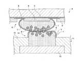
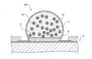
この問題に対する、従来の対策例として、はんだバンプのはんだ(はんだ材料)中に樹脂微粒子を含有させて応力を緩和する方法が挙げられる(たとえば特許文献1参照)。図11は、前記特許文献1に記載された従来のはんだバンプの構造を示すものであり、20ははんだバンプ、1ははんだバンプ20のはんだ(はんだ材料)、2は半導体チップ、3は半導体チップ2の接続電極、21は樹脂微粒子である。図11に示すように、はんだバンプ20のはんだ1中に、樹脂微粒子21がほぼ均一に分散した状態で含有されており、樹脂微粒子21の弾性により、冷却時に発生する応力を緩和させるよう図られている。 As an example of conventional measures against this problem, there is a method in which resin fine particles are contained in solder (solder material) of a solder bump to relieve stress (for example, see Patent Document 1). FIG. 11 shows a structure of a conventional solder bump described in
しかしながら、前記従来のはんだバンプ20の構成では、樹脂微粒子21がはんだバンプ20のはんだ1中にほぼ均一に分散しているため、最も応力が集中する半導体チップ2の接続電極3の外周部(図11に示す場合は、接続電極3にアンダーバンプメタル4が形成されている場合を示しており、この場合にはアンダーバンプメタル4の外周部)に発生する応力を必ずしも十分には緩和できなかった。 However, in the configuration of the
本発明は、上記現状に鑑みて前記課題を解決するもので、高い接続信頼性で半導体チップと基板とを導電接続できるはんだバンプ、このはんだバンプを有する半導体チップ、この半導体チップの製造方法、導電接続構造体、およびこの導電接続構造体の製造方法を提供することを目的とする。 The present invention solves the above-mentioned problems in view of the above-mentioned present situation. A solder bump capable of conductively connecting a semiconductor chip and a substrate with high connection reliability, a semiconductor chip having the solder bump, a method of manufacturing the semiconductor chip, a conductive It is an object of the present invention to provide a connection structure and a method for manufacturing the conductive connection structure.
上記目的を達成するために、本発明のはんだバンプは、半導体チップの接続電極に設けられ、前記半導体チップの接続電極と基板とを接続するはんだバンプであって、前記はんだバンプのはんだよりも熱膨張率が低いフィラーを含有し、先端部のフィラーの密度が、基部のフィラー密度より大きいことを特徴とする。 In order to achieve the above object, the solder bump of the present invention is provided on a connection electrode of a semiconductor chip and connects the connection electrode of the semiconductor chip and a substrate, and is more heat-resistant than the solder of the solder bump. It contains a filler with a low expansion coefficient, and the density of the filler at the tip is larger than the filler density at the base.
なお、フィラーは、表面が多孔質である。フィラーの表面が多孔質であると、はんだの接合時に、はんだの表面に生じることが多い酸化膜を、フィラーでより良好に破壊できて、良好に接合できる。また、フィラーは、線膨張係数が0.1×10⁻⁶/℃〜11×10−6/℃で、かつ比重が1.0g/cm3〜6.0g/cm3であることが好ましい。Incidentally, the filler, the surface ofRu porousder. When the surface of the filler is porous, an oxide film often generated on the surface of the solder can be destroyed more favorably with the filler and can be joined better. Further, the filler is preferably a linear expansion coefficient at0.1 × 10 -6 / ℃ ~11 × 10 -6 / ℃, and specific gravity of1.0g / cm 3 ~6.0g / cm 3 .
また、本発明の半導体チップは、前記はんだバンプを有することを特徴とする。また、本発明の半導体チップは、前記はんだバンプが、アンダーバンプメタルを介して半導体チップの接続電極に設けられており、前記アンダーバンプメタルに段差部が形成され、前記はんだバンプの基部が、前記段差部を包含する姿勢で設けられていることを特徴とする。このように、半導体チップの接続電極に設けられたアンダーバンプメタルに段差部が形成されていると、アンダーバンプメタルとはんだバンプとが接合する段差部に集中してフィラーが偏析するため、応力集中を効果的に軽減できてクラックの発生を防止できる。 The semiconductor chip of the present invention has the solder bump. Further, in the semiconductor chip of the present invention, the solder bump is provided on the connection electrode of the semiconductor chip through an under bump metal, a step portion is formed in the under bump metal, and the base of the solder bump is It is provided with the attitude | position including a step part. In this way, if a step is formed on the under bump metal provided on the connection electrode of the semiconductor chip, the filler is segregated at the step where the under bump metal and the solder bump are joined. Can be effectively reduced and the occurrence of cracks can be prevented.
また、本発明は、はんだバンプを有する半導体チップを製造する方法であって、前記半導体チップにフィラー入りのはんだバンプを形成する形成工程と、前記フィラーを含有したはんだを溶融する溶融工程とを有し、前記溶融工程中で、前記半導体チップの上にはんだバンプが配置されている状態で前記半導体チップに振動を印加して、前記はんだバンプ中で前記フィラーを偏析させることを特徴とする。この方法によれば、半導体チップに振動を印加させることにより、比重の小さいフィラーをはんだバンプの先端部に良好に偏析させることができる。 The present invention is also a method for manufacturing a semiconductor chip having solder bumps, comprising a forming step of forming solder bumps containing filler on the semiconductor chip, and a melting step of melting solder containing the filler. In the melting step, vibration is applied to the semiconductor chip in a state where the solder bump is disposed on the semiconductor chip, and the filler is segregated in the solder bump. According to this method, by applying vibration to the semiconductor chip, it is possible to satisfactorily segregate the filler having a small specific gravity on the tip end portion of the solder bump.
また、本発明の導電接続構造体は、半導体チップの接続電極に設けられたはんだバンプと、基板に設けられたはんだ部とが接合されてなるはんだ接合部を有し、前記はんだ接合部を介して前記半導体チップが前記基板に実装された導電接続構造体であって、前記はんだ接合部のはんだよりも熱膨張率が低いフィラーを含有し、前記はんだ接合部における接続電極側部分のフィラーの密度が前記基板側のフィラー密度より大きく、フィラーは、表面が多孔質であることを特徴とする。なお、好ましくは、前記はんだ接合部における接続電極側部分のフィラー密度が、20〜50体積%であるとよく、さらに好ましくは、前記はんだ接合部における接続電極側部分のフィラー密度が、35〜50体積%であるとよい。The conductive connection structure of the present invention has a solder joint formed by joining a solder bump provided on a connection electrode of a semiconductor chip and a solder part provided on a substrate, with the solder joint interposed therebetween. The semiconductor chip is a conductive connection structure mounted on the substrate, and contains a filler having a lower coefficient of thermal expansion than the solder of the solder joint, and the density of the filler on the connection electrode side portion in the solder joint Thererather larger than the filler density of thesubstrate, the filler, wherein asurface is porous. In addition, Preferably, the filler density of the connection electrode side part in the said solder joint part is good in it being 20-50 volume%, More preferably, the filler density of the connection electrode side part in the said solder joint part is 35-50. It is good that it is volume%.
本構成によって、はんだ接合部における接続電極側部分のはんだ材料の一部が、熱膨張率が低いフィラーに置き換えられた状態となるので、はんだ冷却凝固時の、はんだ接合部の接続電極側部分の収縮量が前記フィラーにより減少し、はんだ接合部と半導体チップの接続電極との接合部分のクラックを防止することができる。 With this configuration, a part of the solder material on the connection electrode side portion in the solder joint portion is replaced with a filler having a low coefficient of thermal expansion. The amount of shrinkage is reduced by the filler, and cracks at the joint between the solder joint and the connection electrode of the semiconductor chip can be prevented.
また、本発明の導電接続構造体は、前記はんだ接合部が、アンダーバンプメタルを介して半導体チップの接続電極に接続されており、前記アンダーバンプメタルに段差部が形成され、前記はんだ接合部の前記アンダーバンプメタルとの接続部が、前記段差部を包含する姿勢で設けられていることを特徴とする。このように、半導体チップの接続電極に設けられたアンダーバンプメタルに段差部が形成されていると、アンダーバンプメタルとはんだ接合部とが接合する段差部に集中してフィラーが偏析するため、応力集中を効果的に軽減できてクラックの発生を防止できる。 In the conductive connection structure of the present invention, the solder joint is connected to a connection electrode of a semiconductor chip through an under bump metal, a step portion is formed in the under bump metal, and the solder joint The connection part with the under bump metal is provided in a posture including the step part. Thus, if a step is formed in the under bump metal provided on the connection electrode of the semiconductor chip, the filler is segregated by concentrating on the step where the under bump metal and the solder joint are joined. Concentration can be reduced effectively and cracks can be prevented.
また、本発明は、前記導電接続構造体を製造する方法であって、前記半導体チップを基板の所定位置に接触させる配置工程と、前記半導体チップのはんだバンプを溶融させる溶融工程とを有し、前記溶融工程において、前記基板の上に前記半導体前記チップが配置されている状態で基板または前記半導体チップに振動を印加することで、前記はんだバンプ中で前記フィラーを偏析させて前記はんだ接合部を形成することを特徴とする。この方法によれば、基板または半導体チップに振動を印加させることにより、比重の小さいフィラーをはんだ接合部の接続電極側箇所に良好に偏析させることができる。 Further, the present invention is a method for manufacturing the conductive connection structure, comprising a placement step of bringing the semiconductor chip into contact with a predetermined position of the substrate, and a melting step of melting the solder bumps of the semiconductor chip, In the melting step, by applying vibration to the substrate or the semiconductor chip in a state where the semiconductor chip is disposed on the substrate, the filler is segregated in the solder bump to form the solder joint portion. It is characterized by forming. According to this method, by applying vibration to the substrate or the semiconductor chip, it is possible to satisfactorily segregate the filler having a small specific gravity on the connection electrode side portion of the solder joint.
本発明のはんだバンプや、はんだバンプを有する半導体チップ、導電接続構造体を用いることで、半導体チップと基板との接合部分のクラックを防止することができて、ひいては導電接続構造体の信頼性を向上することができる。 By using the solder bump of the present invention, a semiconductor chip having a solder bump, and a conductive connection structure, it is possible to prevent cracks at the joint portion between the semiconductor chip and the substrate, and thus improve the reliability of the conductive connection structure. Can be improved.
以下、本発明の実施の形態について、図面を参照しながら説明する。
(実施の形態1)
図1および図2は、本発明の実施の形態1に係るはんだ接合部およびはんだバンプの断面図である。なお、図1、図2において、図11に示す従来のはんだバンプ20と同じ構成要素については同じ符号を用いる。Hereinafter, embodiments of the present invention will be described with reference to the drawings.
(Embodiment 1)
1 and 2 are cross-sectional views of a solder joint and solder bumps according to Embodiment 1 of the present invention. 1 and 2, the same reference numerals are used for the same components as those of the
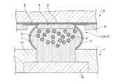
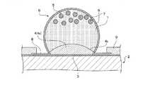
図2に示すように、本発明のはんだバンプ6は、半導体チップ2の接続電極3と基板11とを接続するためのはんだバンプ6であって、はんだバンプ6が微細なフィラー5を含有している。そして、はんだバンプ6の先端部、つまり、はんだバンプ6における接続電極3から離れた箇所の、フィラー密度が、はんだバンプ6の基部、つまり、はんだバンプ6における半導体チップ2の接続電極3近傍箇所の、フィラー密度より大きく構成されている。ここで、フィラー5は、はんだバンプ6のはんだ(はんだ材料)1や後述するはんだプリコート14のはんだ(はんだ材料)1よりも熱膨張率が低いものが用いられている。また、図1に示すように、半導体チップ2に形成されたはんだバンプ6と、基板11の基板電極12に形成されたはんだ部としてのはんだプリコート14とが接合されて、これらのはんだバンプ6とはんだプリコート14との接合体であるはんだ接合部17を介して、半導体チップ2と基板11とが接続されてなる導電接続構造体16が形成(製造)されている。そして、はんだ接合部17のはんだ1よりも熱膨張率が低いフィラー5を含有し、はんだ接合部17における接続電極側3部分のフィラー5の密度が基板11側のフィラー密度より大きく構成されている。 As shown in FIG. 2, the solder bump 6 of the present invention is a solder bump 6 for connecting the
次に、図2〜図6を参照しながら、半導体チップ2と基板11とを接合する前の、半導体チップ2へのはんだバンプ6の形成状態や、基板11へのはんだプリコート14の形成状態、ならびに、これらの半導体チップ2と基板11とが接合されてなる導電接続構造体16の形成(製造)工程などを順に説明する。 Next, referring to FIGS. 2 to 6, the state of formation of the solder bumps 6 on the
図2は、半導体チップ2と基板11とを接合する前の、半導体チップ2へのはんだバンプ6の形成状態を示す断面図である。図2に示すように、半導体チップ2上には、120μmピッチで一般的な接続電極3が形成されており、更に接続電極3上に、ニッケルを主成分としたアンダーバンプメタル(以降、UBMとする)4が形成され、その上に、微細なフィラー5を含有したはんだ1からなるはんだバンプ6が形成されている。本実施の形態では、アルミニウムの接続電極3上に、ニッケルからなるUBM4を無電解メッキにて形成している。また、はんだバンプ6のはんだ1の材料としてはSn−3Ag−0.5Cuを使用した。さらに、接合時のバンプショートを回避しつつ、接合強度を確保するために、UBM4の直径とはんだバンプ6の直径とはそれぞれ60μm、はんだバンプ6の高さを30μmとした。 FIG. 2 is a cross-sectional view showing a state in which the solder bumps 6 are formed on the
はんだバンプ6に含有させるフィラー5の材料は、はんだ1より比重が小さく、熱膨張率(線膨張係数)が低いものが用いられる。このフィラー5の材料としては、シリカ、アルミナ、炭化珪素、窒化珪素、ジルコニア、マイカなどが挙げられる。中でも比重が2.0g/cm3と軽く、線膨張係数が0.5×10−6/℃と非常に小さいシリカが好適である。本実施の形態では、フィラー5の材料として、直径0.5μm、表面積7m2/gの多孔質シリカを採用した。ここで、フィラー5は、線膨張係数が0.1×10−6/℃〜11×10−6/℃で、かつ比重が1.0g/cm3〜6.0g/cm3であることが好ましい。なお、図2において、7ははんだ1の表面に形成された酸化膜、8は半導体チップ2上に形成されているパッシベーション膜、9はPBO(ポリベンゾオキサゾール)などからなる樹脂層である。As the material of the
はんだバンプ6の形成工程(製造工程)としては、予め前記フィラー5を含有したはんだペーストを、半導体チップ2が多数形成された半導体ウェハにマスク印刷した後、バッチ型リフロー装置にて加熱してはんだ1を溶融させ、その後、冷却することによって形成した。 As a solder bump 6 forming process (manufacturing process), a solder paste containing the
なお、はんだ1の供給方法は、前記方法に限らず、例えばメッキ液にフィラー5を混入させ、メッキによって供給する、あるいはフィラー5を含有したはんだボールをはんだボール搭載機で搭載、供給する方法などが挙げられる。また、フィラー5を含有したフラックスを、はんだバンプ6の形成後に塗布、加熱、一体化させることで、フィラー5を後から供給することも可能である。 The method for supplying the
はんだ1の溶融時には、半導体チップ2の上に、はんだバンプ6が配置されている状態で、はんだ1中に含有した比重の小さいフィラー5を、はんだバンプ6の上層に浮上させるために、主に水平方向に振動を加えている。具体的には、Sn−3Ag−0.5Cuのはんだ1はその融点が220℃前後であるため、はんだ1の溶融時の最高温度を250±5℃、10±3secで設定し、この最高温度到達中に半導体チップ2に5μm幅、100KHzで振動を加えた。これにより、はんだバンプ6のはんだ1よりも比重の小さいフィラー5が、はんだ1中を浮き上がり、はんだバンプ6の先端部(上層部)に集まることになる。 When the
このはんだバンプ6を有する半導体チップ2の製造方法によれば、はんだバンプ6の全体ではなく、はんだバンプ6の先端部(上層部)にのみフィラー5を偏析させることが可能であり、本実施の形態では、はんだバンプ6の先端部(上層部)5μm中に、はんだ1との体積比10〜25%で偏析できるよう、フィラー5の含有量を調整している。なお、はんだ1の溶融時に半導体チップ2に振動を加えることにより、フィラー5のはんだバンプ6の先端部への移動が促進され、この際の振動の方向は水平方向でなくても、移動促進効果を有する。しかし、振動方向を水平とすると、フィラー5が上方へ移動し易くなり、短い時間で能率的にフィラー5をはんだバンプ6の先端部(上層部)に集めることができる。 According to the method for manufacturing the
前記のようにして、フィラー5を含有したはんだバンプ6を形成した半導体チップ2が多数形成された半導体ウェハを、一般的な工程と同様に、薄板化、小片化を行う。こうして、フィラー5を含有したはんだバンプ6を接続電極3の表面に有する半導体チップ2が形成される。 As described above, the semiconductor wafer on which a large number of
一方、図3は、はんだ部の一例としてのはんだプリコート(以降、SOPと称す)14を形成した基板11を示している。基板(配線基板)11としては、ビルドアップ基板を採用した。ただし、基板11はビルドアップ基板に限定されるものではなく、接合ピッチやコストの観点から、例えばシリコンインターポーザや一般の樹脂基板を採用することも可能である。この基板11上には、半導体チップ2の接続電極3と対向する位置に、半導体チップ2と同様に基板電極12が形成されている。なお、図3において、15は基板11のソルダーレジストである。 On the other hand, FIG. 3 shows a substrate 11 on which a solder precoat (hereinafter referred to as SOP) 14 as an example of a solder portion is formed. As the substrate (wiring substrate) 11, a build-up substrate was adopted. However, the substrate 11 is not limited to the build-up substrate, and for example, a silicon interposer or a general resin substrate can be adopted from the viewpoint of the bonding pitch and cost. On the substrate 11, a
はんだバンプ6を用いた接続には、基板電極12にもはんだプリコート14を設けて行うことが一般的であり、図3に示すように、本実施の形態では、半導体チップ2のはんだバンプ6と同様に、基板11にもフィラー5を含有させたはんだ1からなるSOP14を形成した。基板11のソルダーレジスト15の開口径は60μm、厚みは35μmであり、ソルダーレジスト15の表面より15±5μm突出するようにSOP14を形成した。SOP14のはんだ1の材料は、半導体チップ2側のはんだバンプ6と同様にSn−3Ag−0.5Cuである。 The connection using the solder bump 6 is generally performed by providing the
SOP14の形成方法は、はんだバンプ6と同様な方法で形成できるが、必ずしも同様な方法に特定されるものではなく、今回は予め前記フィラー5を含有したはんだペーストを基板11にマスク印刷した後、バッチ型リフロー装置にて加熱して、はんだ1を溶融、冷却し、基板内高さバラツキを抑えるために圧延レベリングを実施した。このSOP14の形成にも、半導体チップ2のはんだバンプ6の形成と同様の配置構成(基板11の基板電極12の上方にはんだプリコート14を配置した配置構成)ならびに加熱・水平振幅条件を印加し、SOP14の先端部(上層部)に微細フィラー5を偏析させた。 The method of forming the
次に、上記のようにして形成された半導体チップ2を、基板11上にフリップチップ実装する。今回は、接合ピッチが120μmと狭ピッチであったため、フラックス洗浄の困難さを回避するために、フラックスレスはんだ接合を採用した。 Next, the
まず、図4に示すように、基板11の上方に半導体チップ2を位置させて、半導体チップ2を基板11上に搭載した。半導体チップ2は200℃、基板11は100℃となるように、半導体チップ2側の吸着ツールとステージの温度設定を行った後、半導体チップ2の接続電極3と基板11の基板電極12とが対向する位置で搭載した。この時、はんだバンプ6のはんだ1およびSOP14のはんだ1は溶融しておらず、半導体チップ2へのダメージを考慮して、1バンプ当たり1g程度の荷重で搭載した。 First, as shown in FIG. 4, the
次に、半導体チップ2側の吸着ツールを昇温させ、はんだ1の融点以上である260℃で5sec加熱して、はんだバンプ6のはんだ1およびSOP14のはんだ1を溶融させる。通常、はんだ1の表面には数nm程度の酸化膜7が形成されており、溶融状態のはんだ1を押圧したのみでは、はんだバンプ6とSOP14とは接合されない。そこで、図5に示すように、基板11の上方に半導体チップ2が配置されている状態で、基板1を水平方向に20μm幅、10Hzで5sec振動させ(例えば超音波を印加して振動させ)、はんだ1の酸化膜7同士を擦りあわせることで、酸化膜7の破壊を行っている。本実施の形態によれば、はんだバンプ6とSOP14との接点付近には、フィラー5が偏析しており、はんだ1の溶融時でも固体であるフィラー5は、酸化膜7の破壊に効果的に機能する。本実施の形態では多孔質のフィラー5を採用しており、このように多孔質のフィラー5を採用することで、酸化膜7をより良好に破壊できて更に効果的となる。 Next, the temperature of the suction tool on the
次に、図6に示すように、はんだバンプ6とSOP14との接合点付近から酸化膜7が破壊され、両者の接合が進むにつれて、はんだ1よりも比重の小さいフィラー5は、より上層への浮上を開始し、最終的には図1に示すように、はんだバンプ6とSOP14とが接合されてなるはんだ接合部17における、半導体チップ2の接続側電極8側(より詳しくは半導体チップ2のUBM4の近傍、5μm)のはんだ1中に、20〜50%の体積比でフィラー5が偏析する。 Next, as shown in FIG. 6, the
この時、はんだ接合部17と接するUBM4のニッケルとパッシベーション膜8のSiNとの線膨張係数はともに14×10−6/℃であり、はんだ接合部17におけるUBM4近傍のはんだ1中に体積比で約37%のフィラー5が偏析したとき、UBM4及びパッシベーション膜8の線膨張係数と、フィラー5を含んだはんだ1の見かけ上の線膨張係数がほぼ一致し、半導体チップ2の接続電極3近傍の応力を大幅に低減することができる。At this time, the linear expansion coefficients of the nickel of
はんだ接合部17の接続電極3(UBM4)近傍箇所の最適なフィラー5の含有量は、はんだ1とフィラー5との組合せによって異なり、例えばSn−3Ag−0.5Cuのはんだ1に対して、炭化珪素の場合は約45%、窒化珪素の場合は約42%が最適なフィラー5の含有量となる。よって、好ましくは、35〜50%の体積比でフィラー5が偏析するのがよい。 The
ここで、フィラー5の含有量が最適値に大きく満たない場合、フィラー5を含んだはんだ1の見かけ上の線膨張係数と、UBM4及びパッシベーション膜8の線膨張係数との格差が縮まらず、応力低減効果が低下する。一方、フィラー5の含有量が体積比50%を超えると、半導体チップ2の接続電極3と基板電極12との接続抵抗が上昇するため、電気特性を満たすことが困難になる。 Here, when the content of the
その後、半導体チップ2側の吸着ツールを200℃まで冷却することで、はんだ接合部17のはんだ1を凝固させ、導電接続構造体16を形成する。この後、半導体チップ2と基板11との間隙にアンダーフィル材を充填、硬化させることで、実装構造として完成となる。 Thereafter, the suction tool on the
かかる構成によれば、はんだ接合部17における、半導体チップ2のUBM4近傍に温度変化に対する伸縮量(すなわち熱膨張率)が低いフィラー5が偏析し、温度変化に対する伸縮量が低減する。したがって、はんだ冷却凝固時の、半導体チップ2の接続電極3近傍のはんだバンプ6の収縮量がフィラー5により減少して、前記収縮による応力の発生も減少し、はんだ接合部17における半導体チップ2の接続電極3との接合部分近傍箇所のクラックの発生を防止することができる。この結果、導電接続構造体16の信頼性を向上することができる。 According to this configuration, the
(実施の形態2)
図7、図8は、本発明の実施の形態2におけるはんだ接合部17やはんだバンプ6などの断面図であり、図7は、導電接続構造体16が形成された状態でのはんだ接合部17などの断面図を示し、図8は、基板11と接合される前の、はんだバンプ6を半導体チップ2に形成した状態のはんだバンプ6の断面図である。なお、図7、図8において、実施の形態1と同じ構成要素については同じ符号を用い、説明を省略する。(Embodiment 2)
7 and 8 are cross-sectional views of the solder joints 17 and the solder bumps 6 in
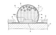
図7、図8に示すように、この実施の形態2においては、半導体チップ2の接続電極3上に、ニッケルを主成分としたUBM4を、段差部4cを有する凸型に形成している点が、上記実施の形態1とは異なっている。ここで、UBM4の形状、形成方法は、中央部4aと周縁部4bとに高低差があり(中央部4aが高く、周縁部4bが低ければ)、段差部4cを有していれば限定されるものではなく、例えば、電解メッキを複数回行うことで、階段状にすることで高低差とする方法などが挙げられる。本実施の形態では、図8に示すように、アルミニウムの接続電極3上に、電解ニッケルメッキで60μm径1μm厚で形成した後、40μm径3μm厚で2段目のメッキを行うことで階段状の段差部4cを有するUBM4を形成した。 As shown in FIGS. 7 and 8, in the second embodiment, the
この後、実施の形態1と同様の工程を経て、はんだバンプ6の形成、SOP14の形成、および半導体チップ2と基板11との接続を行い、図7に示すような導電接続構造体18を形成した。 Thereafter, through the same steps as in the first embodiment, the formation of the solder bump 6, the formation of the
かかる構造によれば、図7に示すように、最も応力が集中する半導体チップ2の接続電極3の周縁部(この実施の形態では、UBM4の周縁部4b)に形成された段差部4cに集中してフィラー5が偏析するため、より効果的に半導体チップ2の接続電極3近傍の応力を低減することができる。したがって、クラックの発生をより確実に防止することができ、さらに、はんだ接合部17と広い面積で平面状に接する中央部4a付近のフィラー5を少なめに抑えることができるため、フィラー5の含有による接続抵抗の上昇を抑えることができる。 According to such a structure, as shown in FIG. 7, the stress is concentrated on the stepped
なお、上記のように、UBM4に階段状の段差部4cを形成することにより、極めて良好にUBM4の段差部4cや周縁部4bの近傍に集中してフィラー5を偏析させることができて、クラックの発生を確実に防止することができるが、これに限るものではない。すなわち、図9に示すように、無電解メッキにて、高アスペクトのUBM4を形成し、周縁部の曲線をもって高低差としても、図10に示すように、UBM4の周縁部4bの近傍に集中してフィラー5を偏析させることができて、クラックの発生をより確実に防止することができると同時に、フィラー5の含有による接続抵抗の上昇を抑えることができる。 As described above, by forming the stepped
本発明に係るはんだバンプ、半導体チップ、半導体チップの製造方法、導電接続構造体、および導電接続構造体の形成方法は、半導体チップと基板とをはんだバンプを介して接続する各種の導電接続構造体に適用できる。 A solder bump, a semiconductor chip, a method for manufacturing a semiconductor chip, a conductive connection structure, and a method for forming a conductive connection structure according to the present invention include various conductive connection structures for connecting a semiconductor chip and a substrate via solder bumps. Applicable to.
1 はんだ
2 半導体チップ
3 接続電極
4 アンダーバンプメタル(UBM)
5 微細フィラー
6 はんだバンプ
7 酸化膜
8 パッシベーション膜
9 樹脂層
11 基板(配線基板)
12 基板電極
14 はんだプリコート
15 ソルダーレジスト
16、18 導電接続構造体
17 はんだ接合部1
5 Fine filler 6
12
Claims (11)
Translated fromJapanese前記半導体チップにフィラー入りのはんだバンプを形成する形成工程と、
前記フィラーを含有したはんだを溶融する溶融工程とを有し、
前記溶融工程中で、前記半導体チップの上にはんだバンプが配置されている状態で前記半導体チップに振動を印加して、前記はんだバンプ中で前記フィラーを偏析させることを特徴とする半導体チップの製造方法。A method of manufacturing a semiconductor chip according to claim3 or 4 ,
Forming a solder bump containing filler on the semiconductor chip; and
A melting step of melting the solder containing the filler,
In the melting step, a vibration is applied to the semiconductor chip in a state where a solder bump is disposed on the semiconductor chip, and the filler is segregated in the solder bump. Method.
前記半導体チップを基板の所定位置に接触させる配置工程と、
前記半導体チップのはんだバンプを溶融させる溶融工程とを有し、
前記溶融工程において、前記基板の上に前記半導体前記チップが配置されている状態で基板または前記半導体チップに振動を印加することで、前記はんだバンプ中で前記フィラーを偏析させて前記はんだ接合部を形成することを特徴とする導電接続構造体の製造方法。A method for manufacturing the conductive connection structure according to any one of claims6 to 10 ,
An arrangement step of bringing the semiconductor chip into contact with a predetermined position of the substrate;
A melting step of melting the solder bumps of the semiconductor chip,
In the melting step, by applying vibration to the substrate or the semiconductor chip in a state where the semiconductor chip is disposed on the substrate, the filler is segregated in the solder bump to form the solder joint portion. A method for manufacturing a conductive connection structure, comprising: forming a conductive connection structure.
Priority Applications (2)
| Application Number | Priority Date | Filing Date | Title |
|---|---|---|---|
| JP2010028342AJP5542470B2 (en) | 2009-02-20 | 2010-02-12 | Solder bump, semiconductor chip, semiconductor chip manufacturing method, conductive connection structure, and conductive connection structure manufacturing method |
| US12/707,872US8154123B2 (en) | 2009-02-20 | 2010-02-18 | Solder bump, semiconductor chip, method of manufacturing the semiconductor chip, conductive connection structure, and method of manufacturing the conductive connection structure |
Applications Claiming Priority (3)
| Application Number | Priority Date | Filing Date | Title |
|---|---|---|---|
| JP2009037258 | 2009-02-20 | ||
| JP2009037258 | 2009-02-20 | ||
| JP2010028342AJP5542470B2 (en) | 2009-02-20 | 2010-02-12 | Solder bump, semiconductor chip, semiconductor chip manufacturing method, conductive connection structure, and conductive connection structure manufacturing method |
Publications (2)
| Publication Number | Publication Date |
|---|---|
| JP2010219507A JP2010219507A (en) | 2010-09-30 |
| JP5542470B2true JP5542470B2 (en) | 2014-07-09 |
Family
ID=42630261
Family Applications (1)
| Application Number | Title | Priority Date | Filing Date |
|---|---|---|---|
| JP2010028342AExpired - Fee RelatedJP5542470B2 (en) | 2009-02-20 | 2010-02-12 | Solder bump, semiconductor chip, semiconductor chip manufacturing method, conductive connection structure, and conductive connection structure manufacturing method |
Country Status (2)
| Country | Link |
|---|---|
| US (1) | US8154123B2 (en) |
| JP (1) | JP5542470B2 (en) |
Families Citing this family (8)
| Publication number | Priority date | Publication date | Assignee | Title |
|---|---|---|---|---|
| CN101578694B (en)* | 2006-12-27 | 2011-07-13 | 松下电器产业株式会社 | Conductive bump, method for manufacturing the conductive bump, semiconductor device and method for manufacturing the semiconductor device |
| JP6222909B2 (en)* | 2011-10-07 | 2017-11-01 | キヤノン株式会社 | Multilayer semiconductor device, printed circuit board, and printed wiring board bonding structure |
| JP6326723B2 (en)* | 2012-08-24 | 2018-05-23 | Tdk株式会社 | Terminal structure and semiconductor device |
| JP6155571B2 (en) | 2012-08-24 | 2017-07-05 | Tdk株式会社 | Terminal structure, and semiconductor element and module substrate having the same |
| US8901726B2 (en) | 2012-12-07 | 2014-12-02 | Taiwan Semiconductor Manufacturing Company, Ltd. | Package on package structure and method of manufacturing the same |
| CN113727784A (en)* | 2019-04-30 | 2021-11-30 | 迪睿合株式会社 | Sliding device |
| KR102866334B1 (en) | 2020-08-18 | 2025-09-30 | 삼성전자주식회사 | Semiconductor package and method of manufacturing the semiconductor package |
| CN117976637B (en)* | 2024-04-01 | 2024-07-05 | 甬矽半导体(宁波)有限公司 | Bump package structure and method for manufacturing bump package structure |
Family Cites Families (16)
| Publication number | Priority date | Publication date | Assignee | Title |
|---|---|---|---|---|
| JP2730357B2 (en)* | 1991-11-18 | 1998-03-25 | 松下電器産業株式会社 | Electronic component mounted connector and method of manufacturing the same |
| JP2930186B2 (en) | 1996-03-28 | 1999-08-03 | 松下電器産業株式会社 | Semiconductor device mounting method and semiconductor device mounted body |
| US5880530A (en)* | 1996-03-29 | 1999-03-09 | Intel Corporation | Multiregion solder interconnection structure |
| JPH1154662A (en)* | 1997-08-01 | 1999-02-26 | Nec Corp | Flip-chip resin-sealed structure and resin-sealing method |
| JPH1187424A (en) | 1997-09-10 | 1999-03-30 | Hitachi Ltd | Semiconductor device and manufacturing method thereof |
| JP2000332056A (en)* | 1999-05-17 | 2000-11-30 | Sony Corp | Semiconductor element mounting method and solder paste material |
| JP3645765B2 (en)* | 1999-11-12 | 2005-05-11 | シャープ株式会社 | Solder connection structure, BGA type semiconductor package mounting structure, and BGA type semiconductor package mounting process |
| US6660560B2 (en)* | 2001-09-10 | 2003-12-09 | Delphi Technologies, Inc. | No-flow underfill material and underfill method for flip chip devices |
| US20090008776A1 (en)* | 2006-03-03 | 2009-01-08 | Takashi Kitae | Electronic Component Mounted Body, Electronic Component with Solder Bump, Solder Resin Mixed Material, Electronic Component Mounting Method and Electronic Component Manufacturing Method |
| US7656042B2 (en)* | 2006-03-29 | 2010-02-02 | Taiwan Semiconductor Manufacturing Co., Ltd. | Stratified underfill in an IC package |
| JP2008091650A (en) | 2006-10-03 | 2008-04-17 | Matsushita Electric Ind Co Ltd | Flip chip mounting method and semiconductor package |
| JP4848941B2 (en) | 2006-11-28 | 2011-12-28 | パナソニック株式会社 | Electronic component mounting structure and manufacturing method thereof |
| JP2008218528A (en) | 2007-02-28 | 2008-09-18 | Fujitsu Ltd | Electronic component mounting method and manufacturing apparatus |
| JP5500983B2 (en)* | 2007-03-05 | 2014-05-21 | 京セラ株式会社 | MICROSTRUCTURE DEVICE AND METHOD FOR MANUFACTURING MICROSTRUCTURE DEVICE |
| JP5491856B2 (en)* | 2007-03-19 | 2014-05-14 | ナミックス株式会社 | Anisotropic conductive paste |
| JP2009238969A (en)* | 2008-03-27 | 2009-10-15 | Panasonic Corp | Structure of packaging electronic component and method for manufacturing electronic component packaging body |
- 2010
- 2010-02-12JPJP2010028342Apatent/JP5542470B2/ennot_activeExpired - Fee Related
- 2010-02-18USUS12/707,872patent/US8154123B2/enactiveActive
Also Published As
| Publication number | Publication date |
|---|---|
| US8154123B2 (en) | 2012-04-10 |
| US20100213609A1 (en) | 2010-08-26 |
| JP2010219507A (en) | 2010-09-30 |
Similar Documents
| Publication | Publication Date | Title |
|---|---|---|
| JP5542470B2 (en) | Solder bump, semiconductor chip, semiconductor chip manufacturing method, conductive connection structure, and conductive connection structure manufacturing method | |
| JP3905100B2 (en) | Semiconductor device and manufacturing method thereof | |
| JP6004441B2 (en) | Substrate bonding method, bump forming method, and semiconductor device | |
| JP5645592B2 (en) | Manufacturing method of semiconductor device | |
| TW200525666A (en) | Bump-on-lead flip chip interconnection | |
| JP5897584B2 (en) | Lead-free structure in semiconductor devices | |
| JPWO2005093817A1 (en) | Semiconductor device and manufacturing method thereof | |
| JP2011210773A (en) | Structure and semiconductor device manufacturing method | |
| CN101252093A (en) | Manufacturing method of electronic component and electronic device | |
| TWI502666B (en) | Electronic parts mounting body, electronic parts, substrate | |
| JP5004549B2 (en) | Method for mounting electronic component on substrate and method for forming solder surface | |
| JP2010165923A (en) | Semiconductor device, and method of manufacturing the same | |
| JP2001085470A (en) | Semiconductor device and manufacturing method thereof | |
| JP2013105809A (en) | Semiconductor device and manufacturing method of the same | |
| CN102593067B (en) | Interconnection structure for LGA (Land grid array) packaging with controllable welding spot height and manufacturing method of interconnection structure | |
| JP5919641B2 (en) | Semiconductor device, method for manufacturing the same, and electronic device | |
| JP4720438B2 (en) | Flip chip connection method | |
| JP2015008254A (en) | Circuit board, method of manufacturing the same, method of manufacturing semiconductor device, and method of manufacturing mounting substrate | |
| JP2009009994A (en) | Semiconductor device, and manufacturing method thereof | |
| JP2010123676A (en) | Manufacturing method of semiconductor device and semiconductor device | |
| JP5560713B2 (en) | Electronic component mounting method, etc. | |
| JPH09246319A (en) | Flip chip mounting method | |
| JP4200090B2 (en) | Manufacturing method of semiconductor device | |
| JP2004006926A (en) | Wiring board with solder bump, its manufacturing method, and flattening jig | |
| JP2008192833A (en) | Manufacturing method of semiconductor device |
Legal Events
| Date | Code | Title | Description |
|---|---|---|---|
| A621 | Written request for application examination | Free format text:JAPANESE INTERMEDIATE CODE: A621 Effective date:20121226 | |
| A977 | Report on retrieval | Free format text:JAPANESE INTERMEDIATE CODE: A971007 Effective date:20140121 | |
| A131 | Notification of reasons for refusal | Free format text:JAPANESE INTERMEDIATE CODE: A131 Effective date:20140204 | |
| A521 | Request for written amendment filed | Free format text:JAPANESE INTERMEDIATE CODE: A523 Effective date:20140317 | |
| TRDD | Decision of grant or rejection written | ||
| A01 | Written decision to grant a patent or to grant a registration (utility model) | Free format text:JAPANESE INTERMEDIATE CODE: A01 Effective date:20140408 | |
| A61 | First payment of annual fees (during grant procedure) | Free format text:JAPANESE INTERMEDIATE CODE: A61 Effective date:20140507 | |
| R151 | Written notification of patent or utility model registration | Ref document number:5542470 Country of ref document:JP Free format text:JAPANESE INTERMEDIATE CODE: R151 | |
| LAPS | Cancellation because of no payment of annual fees |