JP5539861B2 - Method for manufacturing a multilayer circuit - Google Patents
Method for manufacturing a multilayer circuitDownload PDFInfo
- Publication number
- JP5539861B2 JP5539861B2JP2010510399AJP2010510399AJP5539861B2JP 5539861 B2JP5539861 B2JP 5539861B2JP 2010510399 AJP2010510399 AJP 2010510399AJP 2010510399 AJP2010510399 AJP 2010510399AJP 5539861 B2JP5539861 B2JP 5539861B2
- Authority
- JP
- Japan
- Prior art keywords
- layer
- opening
- conductive layer
- insulating layer
- electrically insulating
- Prior art date
- Legal status (The legal status is an assumption and is not a legal conclusion. Google has not performed a legal analysis and makes no representation as to the accuracy of the status listed.)
- Expired - Fee Related
Links
- 238000000034methodMethods0.000titleclaimsdescription22
- 238000004519manufacturing processMethods0.000titleclaimsdescription7
- 238000010292electrical insulationMethods0.000claimsdescription20
- 238000004891communicationMethods0.000claimsdescription7
- 230000008878couplingEffects0.000claimsdescription5
- 238000010168coupling processMethods0.000claimsdescription5
- 238000005859coupling reactionMethods0.000claimsdescription5
- 230000002459sustained effectEffects0.000claimsdescription4
- 238000005553drillingMethods0.000claims1
- 239000010408filmSubstances0.000description13
- 239000000853adhesiveSubstances0.000description8
- 230000001070adhesive effectEffects0.000description8
- 238000005286illuminationMethods0.000description8
- 230000008569processEffects0.000description8
- 239000004020conductorSubstances0.000description6
- RYGMFSIKBFXOCR-UHFFFAOYSA-NCopperChemical compound[Cu]RYGMFSIKBFXOCR-UHFFFAOYSA-N0.000description4
- 239000003086colorantSubstances0.000description4
- 239000000463materialSubstances0.000description3
- 239000000615nonconductorSubstances0.000description3
- 239000000758substrateSubstances0.000description3
- OAICVXFJPJFONN-UHFFFAOYSA-NPhosphorusChemical compound[P]OAICVXFJPJFONN-UHFFFAOYSA-N0.000description2
- 238000010924continuous productionMethods0.000description2
- 229910052802copperInorganic materials0.000description2
- 239000010949copperSubstances0.000description2
- 239000011889copper foilSubstances0.000description2
- 239000011888foilSubstances0.000description2
- 239000002184metalSubstances0.000description2
- 229910052751metalInorganic materials0.000description2
- 229920006254polymer filmPolymers0.000description2
- 239000004065semiconductorSubstances0.000description2
- 239000004831Hot glueSubstances0.000description1
- 239000004820Pressure-sensitive adhesiveSubstances0.000description1
- 230000004075alterationEffects0.000description1
- 230000008901benefitEffects0.000description1
- 238000013461designMethods0.000description1
- 238000010586diagramMethods0.000description1
- 239000003365glass fiberSubstances0.000description1
- 238000010030laminatingMethods0.000description1
- 238000010297mechanical methods and processMethods0.000description1
- 230000005226mechanical processes and functionsEffects0.000description1
- 238000012986modificationMethods0.000description1
- 230000004048modificationEffects0.000description1
- 239000012788optical filmSubstances0.000description1
- 238000000059patterningMethods0.000description1
- 229920003223poly(pyromellitimide-1,4-diphenyl ether)Polymers0.000description1
- 229920001721polyimidePolymers0.000description1
- 238000012545processingMethods0.000description1
- 238000001228spectrumMethods0.000description1
Images


Classifications
- H—ELECTRICITY
- H05—ELECTRIC TECHNIQUES NOT OTHERWISE PROVIDED FOR
- H05K—PRINTED CIRCUITS; CASINGS OR CONSTRUCTIONAL DETAILS OF ELECTRIC APPARATUS; MANUFACTURE OF ASSEMBLAGES OF ELECTRICAL COMPONENTS
- H05K3/00—Apparatus or processes for manufacturing printed circuits
- H05K3/46—Manufacturing multilayer circuits
- H05K3/4611—Manufacturing multilayer circuits by laminating two or more circuit boards
- H05K3/4638—Aligning and fixing the circuit boards before lamination; Detecting or measuring the misalignment after lamination; Aligning external circuit patterns or via connections relative to internal circuits
- H—ELECTRICITY
- H05—ELECTRIC TECHNIQUES NOT OTHERWISE PROVIDED FOR
- H05K—PRINTED CIRCUITS; CASINGS OR CONSTRUCTIONAL DETAILS OF ELECTRIC APPARATUS; MANUFACTURE OF ASSEMBLAGES OF ELECTRICAL COMPONENTS
- H05K3/00—Apparatus or processes for manufacturing printed circuits
- H05K3/46—Manufacturing multilayer circuits
- H—ELECTRICITY
- H05—ELECTRIC TECHNIQUES NOT OTHERWISE PROVIDED FOR
- H05K—PRINTED CIRCUITS; CASINGS OR CONSTRUCTIONAL DETAILS OF ELECTRIC APPARATUS; MANUFACTURE OF ASSEMBLAGES OF ELECTRICAL COMPONENTS
- H05K1/00—Printed circuits
- H05K1/02—Details
- H05K1/0213—Electrical arrangements not otherwise provided for
- H05K1/0216—Reduction of cross-talk, noise or electromagnetic interference
- H05K1/0218—Reduction of cross-talk, noise or electromagnetic interference by printed shielding conductors, ground planes or power plane
- H05K1/0224—Patterned shielding planes, ground planes or power planes
- H—ELECTRICITY
- H05—ELECTRIC TECHNIQUES NOT OTHERWISE PROVIDED FOR
- H05K—PRINTED CIRCUITS; CASINGS OR CONSTRUCTIONAL DETAILS OF ELECTRIC APPARATUS; MANUFACTURE OF ASSEMBLAGES OF ELECTRICAL COMPONENTS
- H05K3/00—Apparatus or processes for manufacturing printed circuits
- H05K3/0097—Processing two or more printed circuits simultaneously, e.g. made from a common substrate, or temporarily stacked circuit boards
- H—ELECTRICITY
- H05—ELECTRIC TECHNIQUES NOT OTHERWISE PROVIDED FOR
- H05K—PRINTED CIRCUITS; CASINGS OR CONSTRUCTIONAL DETAILS OF ELECTRIC APPARATUS; MANUFACTURE OF ASSEMBLAGES OF ELECTRICAL COMPONENTS
- H05K3/00—Apparatus or processes for manufacturing printed circuits
- H05K3/30—Assembling printed circuits with electric components, e.g. with resistor
- H05K3/303—Surface mounted components, e.g. affixing before soldering, aligning means, spacing means
- H—ELECTRICITY
- H05—ELECTRIC TECHNIQUES NOT OTHERWISE PROVIDED FOR
- H05K—PRINTED CIRCUITS; CASINGS OR CONSTRUCTIONAL DETAILS OF ELECTRIC APPARATUS; MANUFACTURE OF ASSEMBLAGES OF ELECTRICAL COMPONENTS
- H05K3/00—Apparatus or processes for manufacturing printed circuits
- H05K3/46—Manufacturing multilayer circuits
- H05K3/4611—Manufacturing multilayer circuits by laminating two or more circuit boards
- H05K3/4626—Manufacturing multilayer circuits by laminating two or more circuit boards characterised by the insulating layers or materials
- H05K3/4635—Manufacturing multilayer circuits by laminating two or more circuit boards characterised by the insulating layers or materials laminating flexible circuit boards using additional insulating adhesive materials between the boards
- H—ELECTRICITY
- H05—ELECTRIC TECHNIQUES NOT OTHERWISE PROVIDED FOR
- H05K—PRINTED CIRCUITS; CASINGS OR CONSTRUCTIONAL DETAILS OF ELECTRIC APPARATUS; MANUFACTURE OF ASSEMBLAGES OF ELECTRICAL COMPONENTS
- H05K1/00—Printed circuits
- H05K1/02—Details
- H05K1/0213—Electrical arrangements not otherwise provided for
- H05K1/0237—High frequency adaptations
- H05K1/025—Impedance arrangements, e.g. impedance matching, reduction of parasitic impedance
- H05K1/0253—Impedance adaptations of transmission lines by special lay-out of power planes, e.g. providing openings
- H—ELECTRICITY
- H05—ELECTRIC TECHNIQUES NOT OTHERWISE PROVIDED FOR
- H05K—PRINTED CIRCUITS; CASINGS OR CONSTRUCTIONAL DETAILS OF ELECTRIC APPARATUS; MANUFACTURE OF ASSEMBLAGES OF ELECTRICAL COMPONENTS
- H05K1/00—Printed circuits
- H05K1/02—Details
- H05K1/03—Use of materials for the substrate
- H05K1/0393—Flexible materials
- H—ELECTRICITY
- H05—ELECTRIC TECHNIQUES NOT OTHERWISE PROVIDED FOR
- H05K—PRINTED CIRCUITS; CASINGS OR CONSTRUCTIONAL DETAILS OF ELECTRIC APPARATUS; MANUFACTURE OF ASSEMBLAGES OF ELECTRICAL COMPONENTS
- H05K1/00—Printed circuits
- H05K1/18—Printed circuits structurally associated with non-printed electric components
- H05K1/189—Printed circuits structurally associated with non-printed electric components characterised by the use of a flexible or folded printed circuit
- H—ELECTRICITY
- H05—ELECTRIC TECHNIQUES NOT OTHERWISE PROVIDED FOR
- H05K—PRINTED CIRCUITS; CASINGS OR CONSTRUCTIONAL DETAILS OF ELECTRIC APPARATUS; MANUFACTURE OF ASSEMBLAGES OF ELECTRICAL COMPONENTS
- H05K2201/00—Indexing scheme relating to printed circuits covered by H05K1/00
- H05K2201/03—Conductive materials
- H05K2201/0332—Structure of the conductor
- H05K2201/0335—Layered conductors or foils
- H05K2201/0355—Metal foils
- H—ELECTRICITY
- H05—ELECTRIC TECHNIQUES NOT OTHERWISE PROVIDED FOR
- H05K—PRINTED CIRCUITS; CASINGS OR CONSTRUCTIONAL DETAILS OF ELECTRIC APPARATUS; MANUFACTURE OF ASSEMBLAGES OF ELECTRICAL COMPONENTS
- H05K2201/00—Indexing scheme relating to printed circuits covered by H05K1/00
- H05K2201/09—Shape and layout
- H05K2201/09009—Substrate related
- H05K2201/09063—Holes or slots in insulating substrate not used for electrical connections
- H—ELECTRICITY
- H05—ELECTRIC TECHNIQUES NOT OTHERWISE PROVIDED FOR
- H05K—PRINTED CIRCUITS; CASINGS OR CONSTRUCTIONAL DETAILS OF ELECTRIC APPARATUS; MANUFACTURE OF ASSEMBLAGES OF ELECTRICAL COMPONENTS
- H05K2201/00—Indexing scheme relating to printed circuits covered by H05K1/00
- H05K2201/09—Shape and layout
- H05K2201/09209—Shape and layout details of conductors
- H05K2201/0929—Conductive planes
- H05K2201/09309—Core having two or more power planes; Capacitive laminate of two power planes
- H—ELECTRICITY
- H05—ELECTRIC TECHNIQUES NOT OTHERWISE PROVIDED FOR
- H05K—PRINTED CIRCUITS; CASINGS OR CONSTRUCTIONAL DETAILS OF ELECTRIC APPARATUS; MANUFACTURE OF ASSEMBLAGES OF ELECTRICAL COMPONENTS
- H05K2201/00—Indexing scheme relating to printed circuits covered by H05K1/00
- H05K2201/09—Shape and layout
- H05K2201/09209—Shape and layout details of conductors
- H05K2201/09654—Shape and layout details of conductors covering at least two types of conductors provided for in H05K2201/09218 - H05K2201/095
- H05K2201/09681—Mesh conductors, e.g. as a ground plane
- H—ELECTRICITY
- H05—ELECTRIC TECHNIQUES NOT OTHERWISE PROVIDED FOR
- H05K—PRINTED CIRCUITS; CASINGS OR CONSTRUCTIONAL DETAILS OF ELECTRIC APPARATUS; MANUFACTURE OF ASSEMBLAGES OF ELECTRICAL COMPONENTS
- H05K2201/00—Indexing scheme relating to printed circuits covered by H05K1/00
- H05K2201/09—Shape and layout
- H05K2201/09209—Shape and layout details of conductors
- H05K2201/09654—Shape and layout details of conductors covering at least two types of conductors provided for in H05K2201/09218 - H05K2201/095
- H05K2201/0969—Apertured conductors
- H—ELECTRICITY
- H05—ELECTRIC TECHNIQUES NOT OTHERWISE PROVIDED FOR
- H05K—PRINTED CIRCUITS; CASINGS OR CONSTRUCTIONAL DETAILS OF ELECTRIC APPARATUS; MANUFACTURE OF ASSEMBLAGES OF ELECTRICAL COMPONENTS
- H05K2201/00—Indexing scheme relating to printed circuits covered by H05K1/00
- H05K2201/10—Details of components or other objects attached to or integrated in a printed circuit board
- H05K2201/10007—Types of components
- H05K2201/10106—Light emitting diode [LED]
- H—ELECTRICITY
- H05—ELECTRIC TECHNIQUES NOT OTHERWISE PROVIDED FOR
- H05K—PRINTED CIRCUITS; CASINGS OR CONSTRUCTIONAL DETAILS OF ELECTRIC APPARATUS; MANUFACTURE OF ASSEMBLAGES OF ELECTRICAL COMPONENTS
- H05K2203/00—Indexing scheme relating to apparatus or processes for manufacturing printed circuits covered by H05K3/00
- H05K2203/06—Lamination
- H05K2203/063—Lamination of preperforated insulating layer
- H—ELECTRICITY
- H05—ELECTRIC TECHNIQUES NOT OTHERWISE PROVIDED FOR
- H05K—PRINTED CIRCUITS; CASINGS OR CONSTRUCTIONAL DETAILS OF ELECTRIC APPARATUS; MANUFACTURE OF ASSEMBLAGES OF ELECTRICAL COMPONENTS
- H05K2203/00—Indexing scheme relating to apparatus or processes for manufacturing printed circuits covered by H05K3/00
- H05K2203/15—Position of the PCB during processing
- H05K2203/1545—Continuous processing, i.e. involving rolls moving a band-like or solid carrier along a continuous production path
- H—ELECTRICITY
- H05—ELECTRIC TECHNIQUES NOT OTHERWISE PROVIDED FOR
- H05K—PRINTED CIRCUITS; CASINGS OR CONSTRUCTIONAL DETAILS OF ELECTRIC APPARATUS; MANUFACTURE OF ASSEMBLAGES OF ELECTRICAL COMPONENTS
- H05K2203/00—Indexing scheme relating to apparatus or processes for manufacturing printed circuits covered by H05K3/00
- H05K2203/16—Inspection; Monitoring; Aligning
- H05K2203/166—Alignment or registration; Control of registration
- H—ELECTRICITY
- H05—ELECTRIC TECHNIQUES NOT OTHERWISE PROVIDED FOR
- H05K—PRINTED CIRCUITS; CASINGS OR CONSTRUCTIONAL DETAILS OF ELECTRIC APPARATUS; MANUFACTURE OF ASSEMBLAGES OF ELECTRICAL COMPONENTS
- H05K3/00—Apparatus or processes for manufacturing printed circuits
- H05K3/10—Apparatus or processes for manufacturing printed circuits in which conductive material is applied to the insulating support in such a manner as to form the desired conductive pattern
- H05K3/20—Apparatus or processes for manufacturing printed circuits in which conductive material is applied to the insulating support in such a manner as to form the desired conductive pattern by affixing prefabricated conductor pattern
- H05K3/202—Apparatus or processes for manufacturing printed circuits in which conductive material is applied to the insulating support in such a manner as to form the desired conductive pattern by affixing prefabricated conductor pattern using self-supporting metal foil pattern
- H—ELECTRICITY
- H05—ELECTRIC TECHNIQUES NOT OTHERWISE PROVIDED FOR
- H05K—PRINTED CIRCUITS; CASINGS OR CONSTRUCTIONAL DETAILS OF ELECTRIC APPARATUS; MANUFACTURE OF ASSEMBLAGES OF ELECTRICAL COMPONENTS
- H05K3/00—Apparatus or processes for manufacturing printed circuits
- H05K3/38—Improvement of the adhesion between the insulating substrate and the metal
- H05K3/386—Improvement of the adhesion between the insulating substrate and the metal by the use of an organic polymeric bonding layer, e.g. adhesive
- Y—GENERAL TAGGING OF NEW TECHNOLOGICAL DEVELOPMENTS; GENERAL TAGGING OF CROSS-SECTIONAL TECHNOLOGIES SPANNING OVER SEVERAL SECTIONS OF THE IPC; TECHNICAL SUBJECTS COVERED BY FORMER USPC CROSS-REFERENCE ART COLLECTIONS [XRACs] AND DIGESTS
- Y10—TECHNICAL SUBJECTS COVERED BY FORMER USPC
- Y10T—TECHNICAL SUBJECTS COVERED BY FORMER US CLASSIFICATION
- Y10T29/00—Metal working
- Y10T29/49—Method of mechanical manufacture
- Y10T29/49002—Electrical device making
- Y10T29/49117—Conductor or circuit manufacturing
- Y10T29/49124—On flat or curved insulated base, e.g., printed circuit, etc.
- Y10T29/4913—Assembling to base an electrical component, e.g., capacitor, etc.
Landscapes
- Engineering & Computer Science (AREA)
- Microelectronics & Electronic Packaging (AREA)
- Manufacturing & Machinery (AREA)
- Physics & Mathematics (AREA)
- Electromagnetism (AREA)
- Structure Of Printed Boards (AREA)
- Fastening Of Light Sources Or Lamp Holders (AREA)
- Manufacturing Of Printed Wiring (AREA)
- Led Device Packages (AREA)
- Production Of Multi-Layered Print Wiring Board (AREA)
Description
Translated fromJapanese本出願は、回路、例えばフレキシブル回路を目的とする。 The present application is directed to circuits, such as flexible circuits.
回路及び調光装置を使用する照明装置は、当該技術分野において多数の応用例で知られている。そのような装置は、光源と、その光源に電力を供給するための電気回路と、所望の方式で光源によって生成された光を方向付けるための反射体又は拡散体などの何らかの調光装置とを包含している。そのような装置は、特に、とりわけ薄い光導体又は調光装置の場合に、最小の空間利用率で照明を提供する試みのために使用されてもよい。しかしながら、主として照明を提供するために使用される既知の光装置及び取り付け具は、典型的には、白熱電球の取り付け具などの点灯装置又は類似の点灯装置を収容する嵩高いハウジングを利用する。例えば、看板、チャネル文字、及びディスプレイなどの特定の応用例において、これらの既知の照明装置は、比較的大きな空間を利用する。 Lighting devices that use circuits and dimmers are known in the art for numerous applications. Such a device comprises a light source, an electrical circuit for supplying power to the light source, and some dimming device such as a reflector or diffuser for directing light generated by the light source in a desired manner. Is included. Such devices may be used for attempts to provide illumination with minimal space utilization, especially in the case of thin light guides or dimmers. However, known light devices and fixtures used primarily to provide illumination typically utilize a bulky housing that houses a lighting device such as an incandescent bulb fixture or similar lighting device. For example, in certain applications such as billboards, channel letters, and displays, these known lighting devices utilize a relatively large space.
回路基板を用いる点灯装置は、銅回路と構成要素用の取り付け穴とでパターン形成されたガラス繊維基板であってもよい。そのような硬質な回路基板は、FR4回路基板として知られるものであり、設計により、曲がらない及び硬質なものになるように作製される。そのため、それらは、平坦でない表面の上に取り付けるためには好適でない。フレキシブル回路が存在し、及び典型的には、商標名カプトン(KAPTON)ポリイミドフィルムにより販売されているもののようなフィルム上にパターン形成された銅から作製されている。これらの回路は、柔軟性という利益を提供するが、製造コストがより高いという欠点がある。加えて、これらの回路は、典型的には、ステップアンドリピートのパターン形成プロセスによって作製される。そのようなプロセスは、層上で特徴を位置合わせする上で、及びまた層間の接続を行う上でも相当な困難をもたらす。 The lighting device using a circuit board may be a glass fiber substrate patterned with a copper circuit and component mounting holes. Such rigid circuit boards are known as FR4 circuit boards and are made by design to bend and be rigid. As such, they are not suitable for mounting on uneven surfaces. Flexible circuits exist and are typically made from copper patterned on a film such as that sold by the trade name KAPTON polyimide film. These circuits offer the benefit of flexibility, but have the disadvantage of higher manufacturing costs. In addition, these circuits are typically made by a step-and-repeat patterning process. Such a process presents considerable difficulty in aligning features on the layers and also in making the connections between the layers.
そのため、そのようなプロセスは高価であり、及び維持費が高額となる。 As a result, such processes are expensive and expensive to maintain.
1つの実施形態では、多層回路を製造する方法は、第1電気絶縁層であって、前記第1電気絶縁層を貫いて画定される少なくとも1つの開口を有する第1電気絶縁層を提供することと、前記第1電気絶縁層を第1導電層と結合することと、第2導電層を提供することと、前記第2導電層を、前記第1導電層とは反対側で前記第1電気絶縁層に結合することと、第2電気絶縁層を提供することと、前記第2電気絶縁層を、前記第1電気絶縁層とは反対側で前記第2導電層に結合することと、前記第2電気絶縁層に、少なくとも2つの端子を有する少なくとも1つの光源を配置することと、を含み、前記第1導電層が、前記第1電気絶縁層の前記開口と見当合わせして、前記第1電気絶縁層に結合され、前記多層回路が持続速度で製造され、前記第2導電層が、該第2導電層を貫いて画定されると共に前記第1電気絶縁層の前記少なくとも1つの開口と位置合わせするように位置付けられる少なくとも1つの開口を有し、前記第2電気絶縁層は、1対以上の開口群を有し、前記開口群のそれぞれは前記第2電気絶縁層を貫いて画定される第1開口と第2開口とを有し、前記第1開口は、前記第1電気絶縁層の前記開口と、前記第2導電層の前記開口とに、位置合わせするように位置付けられていて、前記光源の一方の端子は、前記第1開口、前記第2導電層の前記開口、及び前記第1電気絶縁層の前記開口を通して、前記第1導電層と電気通信し、前記光源の他方の端子は、前記第2開口を通して前記第2導電層と電気通信する、多層回路を製造する方法である。
In one embodiment,a method of manufacturing a multilayer circuit provides a first electrical insulation layer having a first electrical insulation layer having at least one opening defined through the first electrical insulation layer. Coupling the first electrical insulating layer with the first conductive layer, providing a second conductive layer, and connecting the second conductive layer to the first electrical layer on the opposite side of the first conductive layer. Coupling to an insulating layer; providing a second electrical insulation layer; coupling the second electrical insulation layer to the second conductive layer on the opposite side of the first electrical insulation layer; Disposing at least one light source having at least two terminals on a second electrical insulation layer, wherein the first conductive layer is in registration with the opening of the first electrical insulation layer, Coupled to one electrical insulating layer, the multilayer circuit is manufactured at a sustained rate, Two conductive layers having at least one opening defined through the second conductive layer and positioned to align with the at least one opening of the first electrical insulating layer; The layer has one or more pairs of openings, each of the openings having a first opening and a second opening defined through the second electrically insulating layer, the first opening being The opening of the first electrical insulating layer and the opening of the second conductive layer are positioned so as to be aligned, and one terminal of the light source is connected to the first opening and the second conductive layer. A multilayer circuit in electrical communication with the first conductive layer through the opening and the opening in the first electrical insulating layer, and the other terminal of the light source in electrical communication with the second conductive layer through the second opening. It is a method of manufacturing.
別の実施形態では、多層回路を製造する方法は、前記第1電気絶縁層を提供する前に、前記第1電気絶縁層の前記開口を形成するよう、前記第1電気絶縁層を穿孔することを含む、方法である。
In another embodiment,a method of manufacturing a multilayer circuit includes perforating the first electrical insulation layer to form the opening in the first electrical insulation layer before providing the first electrical insulation layer. Including a method.
方法
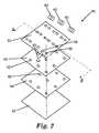
本出願は多層フレキシブル回路を目的とする。回路は、電流を送達することができる。方法は、電気絶縁層を提供することを含む。電気絶縁層は導電層に結合される。層は、永久的結合により結合されてもよいし、又は互いに取り外し可能であってもよい。この接続は、多数の方法で行われてもよい。いくつかの実施形態では、この接続は、機械的プロセスによって行われる。即ちこの結合は、2つの別々の層の間で形成され、及び導電層は、電気絶縁層の上に化学的に被着されていない。例えば、積層プロセス、又は電気絶縁層と導電層とを共に接着剤で接合することである。図1は、本方法の実施形態を例示している。図1では、プロセス10は、電気絶縁層12を含む。電気絶縁層12は次には導電層14と結合される。Method The present application is directed to a multilayer flexible circuit. The circuit can deliver current. The method includes providing an electrically insulating layer. The electrically insulating layer is coupled to the conductive layer. The layers may be bonded by permanent bonding or may be removable from each other. This connection may be made in a number of ways. In some embodiments, this connection is made by a mechanical process. That is, this bond is formed between two separate layers, and the conductive layer is not chemically deposited over the electrically insulating layer. For example, a laminating process, or bonding an electrically insulating layer and a conductive layer together with an adhesive. FIG. 1 illustrates an embodiment of the method. In FIG. 1,
本出願の方法は、持続速度で実行される。持続速度は、本出願の目的上、製造のいずれの段階の間も、回路の区分(最小長さ)が一定速度で動くこととして定義される。例えば方法の各工程において、電気絶縁層及び導電層は、電気絶縁層及び導電層のそれらの区分を含有する結果として生じる多層回路と同じ速度で動く。
The method of the present application is performed at a sustained rate. Sustained speed is defined for the purposes of this application as the section of circuit (minimum length) moves at a constant speed during any stage of manufacture. For example, at each step of the method, the electrically insulating layer and the conductive layer move at the same speed as the resulting multilayer circuit containing those sections of the electrically insulating layer and the conductive layer.
いくつかの実施形態では、電気絶縁層は、この層を導電層に接続する前に穿孔される。穿孔は、電気絶縁層の中に開口を形成する。開口は、電気絶縁層上に、規則的なパターンで又はランダムなパターンで、配置されてもよい。多層回路上のその後に続く層は、次には導電層上の開口と見当合わせされる。本出願の目的上、ある品目が他の品目に関して正しい位置合わせ又は位置付けを有するとき、ある品目は別の品目と見当合わせしている。 In some embodiments, the electrically insulating layer is perforated prior to connecting this layer to the conductive layer. The perforations form openings in the electrically insulating layer. The openings may be arranged on the electrically insulating layer in a regular pattern or a random pattern. Subsequent layers on the multilayer circuit are then registered with openings on the conductive layer. For the purposes of this application, an item is registered with another item when it has the correct alignment or positioning with respect to the other item.
電気絶縁層は、非導電性である。電気絶縁層は、一般に可撓性基材である。特定の実施形態では、電気絶縁層はまた断熱である。他の実施形態では、電気絶縁層は熱伝導性である。いくつかの実施形態では、可撓性基材はポリマーフィルム、例えば光強化フィルムである。 The electrically insulating layer is non-conductive. The electrically insulating layer is generally a flexible substrate. In certain embodiments, the electrically insulating layer is also insulating. In other embodiments, the electrically insulating layer is thermally conductive. In some embodiments, the flexible substrate is a polymer film, such as a light enhanced film.
導電層は一般に自立層であり、及び導電性であるいずれの材料から形成されてもよい。一般に、導電層は、シートに作成され得る材料から形成される。 The conductive layer is generally a self-supporting layer and may be formed from any material that is conductive. Generally, the conductive layer is formed from a material that can be made into a sheet.
導電層は、連続していても、又は不連続であってもよい。導電層が不連続である実施形態では、回路は、導電層が分断される地点で遮断される。導電層は、完全なシートであっても、又はパターンになっていてもよい。好適なパターンの例には、グリッドパターン、連続ストリングパターン、連続/平行パターン、一連の平行パターン、ストリングの平行配列、又はこれらの組み合わせが挙げられる。 The conductive layer may be continuous or discontinuous. In embodiments where the conductive layer is discontinuous, the circuit is interrupted at the point where the conductive layer is broken. The conductive layer may be a complete sheet or a pattern. Examples of suitable patterns include a grid pattern, a continuous string pattern, a continuous / parallel pattern, a series of parallel patterns, a parallel arrangement of strings, or a combination thereof.
本発明に使用される接着剤は、電気絶縁層を導電層に接続するために好適ないずれの接着剤であってもよい。いくつかの実施形態では、接着剤は感圧接着剤である。いくつかの実施形態では、接着剤は、熱処理接着剤、例えばホットメルト接着剤である。 The adhesive used in the present invention may be any adhesive suitable for connecting the electrical insulating layer to the conductive layer. In some embodiments, the adhesive is a pressure sensitive adhesive. In some embodiments, the adhesive is a heat treated adhesive, such as a hot melt adhesive.
多くの実施形態では、多層回路は、第2電気絶縁層及び第2導電層を含む。図1は、第2電気絶縁層16及び第2導電層18を示す。加えて、方法は、多層回路を被覆する底部フィルム19を含んでもよい。この底部フィルムは、追加的電気絶縁層であっても若しくは別個のポリマーフィルムであっても、又は両方の組み合わせであってもよい。 In many embodiments, the multilayer circuit includes a second electrically insulating layer and a second conductive layer. FIG. 1 shows a second
図2は、本出願のプロセスから結果として生じる多層回路の実施形態を例示する。本出願のプロセスにより作製された多層回路の具体的な実施形態は、例えば、本明細書に参考として組み込まれる米国特許出願第60/826,245号(代理人整理番号60609US011)からの優先権を主張する、同時係属出願の米国特許連番___に見出すことができる。第1導電層42は、銅箔、又はシート若しくは層として変形され得る他の好適な導体などの金属箔からなってもよい。第1導体層42上に配置されるのは、第1電気絶縁層又は非導電層44である。いくつかの実施形態では、別の電気絶縁層又は非導電層が、第1導電層42の下に配置されることができ、導電層42を2つの非導電層の間に挟み込む。第1電気絶縁体層44は、この層を貫く1つ以上の開口46を包含する。第1電気絶縁体層44は、上記のように、シート若しくは層として変形され得るいずれの既知の電気絶縁体若しくは誘電体、又は光反射層からなってもよい。加えて、層44は、層44を第1導電層42などの隣接層に接着するために、片側又は両側に接着剤を包含してもよい。 FIG. 2 illustrates an embodiment of a multilayer circuit resulting from the process of the present application. Specific embodiments of multilayer circuits made by the process of the present application are given priority from, for example, US Patent Application No. 60 / 826,245 (Attorney Docket No. 60609US011), which is incorporated herein by reference. Alleged, co-pending US patent serial number ____. The first
図2に示される実施形態では、装置40は更に、第1電気絶縁層44の上面の上に配置された第2導電層48を包含する。追加的な複数の層が、本出願の範囲内において加えられてもよい。第2導電層48は、この層を貫く1つ以上の開口50を包含し、及び銅箔、又はシート若しくは層として変形され得る他の好適な導体などの金属箔からなってもよい。開口50及び46は、位置合わせするか又は互いに見当合わせされるように構成される。最後に、装置40はフィルム層52を包含する。フィルム層52は反射性材料からなってもよく、又は上記の光反射フィルムのように、何らかの他の光操作性を有してもよい。層52は、1対以上の開口54を包含し、各対54は、第1開口56と第2開口58とを有している。第1開口56は、それぞれ第1電気絶縁層44及び第2導電層48の中の穴46及び50と位置合わせするか又は見当合わせしている。図2は、この位置合わせを垂直な一点鎖線で示している。したがって、層52の上面の上に配置された、アノード及びカソード端子を有するLEDのように、少なくとも2つの端子を有する照明源は、開口56、50、及び46を通して第1導電層42と電気的接触を行ってもよい。光照明源の他の端子は、開口58を通して第2導電層48と電気通信をすることができる。いくつかの実施形態では、層52は、第1開口56及び第2開口58の各対54を置き換える単一の大きい開口を包含する。
In the embodiment shown in FIG. 2, the
装置40はまた、1つ以上の光源又は照明源60を包含し、その光源又は照明源60は、2つの接点(即ちアノード及びカソード)を有する1つ以上の発光ダイオード(LED)であってもよいが、これに限定されない。使用されてもよいLEDの例には、白色、赤色、オレンジ色、琥珀色、黄色、緑色、青色、紫色、又は当該技術分野において既知のLEDのいずれかの他の色など様々な色のLEDが挙げられる。LEDはまた、順方向バイアスされるか又は逆方向バイアスされるかに応じて複数の色を発するタイプであっても、又は赤外線若しくは紫外線を発するタイプであってもよい。更に、LEDは、様々なタイプのパッケージされたLED又はむき出しのLEDダイ、並びにモノリシック回路基板タイプの装置又は回路リード線若しくはワイヤーを使用する構成を包含してもよい。 The
第2導体層48の上面又は光学フィルム層52の底面のいずれかが、層48と52とを互いに貼り付けるために、接着剤を包含してもよいことが特筆される。加えて、組み立てられた装置40の層は、互いに積層されて一体型構造を達成する。 It is noted that either the top surface of the
図3は、装置40の全垂直断面距離に伸びる切断線3−3を通る図2の装置の分解組立断面図を例示している。例示されるように、照明源60の一部分62は、位置合わせされた開口56、50、及び46の上方に位置付けられて、部分62と第1導体層42との間の電気通信を可能にする。照明装置60の別の部分64は、開口58の上方に位置付けられ、部分64と第2導電層48との間の電気通信を提供する。それ故に、電圧源66のような電力源は次には、例示されるように、第1及び第2導体層42及び48にわたって接続され、電力を供給して照明源60を駆動してもよい。 FIG. 3 illustrates an exploded cross-sectional view of the apparatus of FIG. 2 through a section line 3-3 extending through the entire vertical cross-sectional distance of the
上述のように、いくつかの実施形態では、光源は小型発光ダイオード(LED)である。この点で、「LED」は、可視、紫外線、又は赤外線にかかわらず、発光するダイオードを指す。それは、従来型又は超放射型の種類のものにかかわらず、「LED」として販売されている非干渉性内蔵型又は封入型の半導体素子を包含する。LEDが紫外線などの非可視光線を発する場合、及びある場合にはLEDが可視光線を発することもあるが、LEDは蛍光体を包含するようにパッケージ化され(又はそれは遠隔配置された蛍光体を照射してもよい)、短波長の光をより長波長の可視光線に変え、ある場合には白色光を発する素子をもたらすこともある。「LEDダイ」は、最も基本的な形態、即ち半導体加工手順によって作製される個々の構成要素又はチップの形態のLEDである。構成要素又はチップは、デバイスに電圧を加えるための電力の印加のために好適な電気接点を包含することができる。構成要素又はチップの個々の層及び他の機能的要素は、典型的には、ウエハスケールで形成され、及び仕上がったウエハは個々の小片部に切られて、多数のLEDダイをもたらすことができる。パッケージ化されたLEDの更なる論議は、前面発光及び側面発光のLEDを包含して、本明細書において提供される。 As described above, in some embodiments, the light source is a small light emitting diode (LED). In this regard, “LED” refers to a diode that emits light, whether visible, ultraviolet, or infrared. It includes incoherent built-in or encapsulated semiconductor elements sold as “LEDs”, whether of the conventional or super-radiant type. When an LED emits invisible light, such as ultraviolet light, and in some cases, the LED emits visible light, the LED is packaged to include a phosphor (or it can be a remotely located phosphor). May also irradiate), converting short-wavelength light into longer-wavelength visible light, and in some cases leading to elements that emit white light. An “LED die” is an LED in its most basic form, that is, in the form of individual components or chips made by semiconductor processing procedures. The component or chip can include electrical contacts suitable for application of power to apply a voltage to the device. Individual layers of components or chips and other functional elements are typically formed on a wafer scale, and the finished wafer can be cut into individual pieces to provide multiple LED dies. . Further discussion of packaged LEDs is provided herein, including front-emitting and side-emitting LEDs.
所望であれば、開示されたバックライトのための照明源として、別個のLED光源の代わりに、又はLED光源に追加して、線形の冷陰極蛍光ランプ(CCFL)又は熱陰極蛍光ランプ(HCFL)などの他の光源が使用され得る。加えて、ハイブリッドシステム、例えば、寒白色及び暖白色を包含する(CCFL/LED)、CCFL/HCFL、例えば異なるスペクトルを発するものなどが使用されてもよい。発光体の組み合わせは広く異なってもよく、LED類及びCCFL類、並びに複数のもの、例えば、複数のCCFL類、異なる色の複数のCCFL類、並びにLED類及びCCFL類などを包含してもよい。 If desired, a linear cold cathode fluorescent lamp (CCFL) or hot cathode fluorescent lamp (HCFL) as an illumination source for the disclosed backlight, instead of or in addition to a separate LED light source Other light sources such as can be used. In addition, hybrid systems, such as cold white and warm white (CCFL / LED), CCFL / HCFL, such as those emitting different spectra may be used. The combination of light emitters may vary widely and may include LEDs and CCFLs, as well as multiple things, such as multiple CCFLs, multiple CCFLs of different colors, and LEDs and CCFLs, etc. .
いくつかの実施形態では、光源は、異なるピーク波長又は色を有する光を生成することができる光源(例えば、赤色、緑色、及び青色LED類の配列)を包含する。 In some embodiments, the light source includes a light source (eg, an array of red, green, and blue LEDs) that can generate light having different peak wavelengths or colors.
いくつかの実施形態では、透明フィルム又は他の光制御フィルムが、光源の電子的構成要素を覆って多層回路に結合される。この透明フィルムは次には光源を外部損傷から保護する。他の実施形態では、半透明フィルムが、光源の電子的構成要素を覆って多層回路に結合される。この半透明フィルムは次には光源を外部損傷から保護し、及び発せられる光を拡散して光の均一性を改善する。 In some embodiments, a transparent film or other light control film is coupled to the multilayer circuit over the electronic components of the light source. This transparent film then protects the light source from external damage. In other embodiments, a translucent film is bonded to the multilayer circuit over the electronic components of the light source. This translucent film then protects the light source from external damage and diffuses the emitted light to improve light uniformity.
本出願に開示された方法は、連続プロセスにおいて実施されてもよい。即ち、多層回路の長さは、層のための供給フィルムの長さによってのみ限定される。方法はまた、ロールツーロール連続プロセス用に設定されてもよい。そのような方法は、毎分約91.44m(300フィート)を超える速度で実施されてもよい。 The methods disclosed in this application may be performed in a continuous process. That is, the length of the multilayer circuit is limited only by the length of the supply film for the layer. The method may also be set up for a roll-to-roll continuous process. Such a method may be performed at speeds in excess of about 300 feet per minute.
追加的実施形態では、多層回路は、そのロールから、より小さい回路を形成するために切断される。 In additional embodiments, the multilayer circuit is cut from its roll to form a smaller circuit.
本発明の様々な修正及び変更が、本発明の趣旨及び範囲から逸脱することなく当業者には明白となるであろう。 Various modifications and alterations of this invention will become apparent to those skilled in the art without departing from the spirit and scope of this invention.
Claims (2)
Translated fromJapanese第1電気絶縁層であって、前記第1電気絶縁層を貫いて画定される少なくとも1つの開口を有する第1電気絶縁層を提供することと、
前記第1電気絶縁層を第1導電層と結合することと、
第2導電層を提供することと、
前記第2導電層を、前記第1導電層とは反対側で前記第1電気絶縁層に結合することと、
第2電気絶縁層を提供することと、
前記第2電気絶縁層を、前記第1電気絶縁層とは反対側で前記第2導電層に結合することと、
前記第2電気絶縁層に、少なくとも2つの端子を有する少なくとも1つの光源を配置することと、を含み、
前記第1導電層は、前記第1電気絶縁層の前記開口に対して位置合わせされて、前記第1電気絶縁層に結合され、
前記第2導電層は、該第2導電層を貫いて画定されると共に前記第1電気絶縁層の前記少なくとも1つの開口と位置合わせするように位置付けられる少なくとも1つの開口を有し、
前記第2電気絶縁層は、1対以上の開口群を有し、前記開口群のそれぞれは、前記第2電気絶縁層を貫いて画定される第1開口と第2開口とを有し、
前記第1開口は、前記第1電気絶縁層の前記開口と、前記第2導電層の前記開口とに、位置合わせするように位置付けられ、
前記光源の一方の端子は、前記第1開口、前記第2導電層の前記開口、及び前記第1電気絶縁層の前記開口を通して、前記第1導電層と電気通信し、前記光源の他方の端子は、前記第2開口を通して前記第2導電層と電気通信する、方法。A method of manufacturing a multilayer circuit at asustained rate ,
Providing a first electrical insulation layer having at least one opening defined through the first electrical insulation layer;
Combining the first electrically insulating layer with a first conductive layer;
Providing a second conductive layer;
Coupling the second conductive layer to the first electrically insulating layer on the opposite side of the first conductive layer;
Providing a second electrically insulating layer;
Coupling the second electrical insulation layer to the second conductive layer on the opposite side of the first electrical insulation layer;
Disposing at least one light source having at least two terminals on the second electrically insulating layer;
The first conductive layerisaligned with the openingof the first electrical insulation layer and coupled to the first electrical insulation layer;
Before Stories second conductive layerhas at least one opening positioned to align with the at least one opening of the first electrically insulating layer with defined through the second conductive layer,
The second electrical insulating layer has a pair of openings, each ofthe openings having a first opening and a second opening defined through the second electrical insulating layer;
The first opening is positioned to align with the opening of the first electrically insulating layer and the opening of the second conductive layer;
One terminal of the light source is in electrical communication with the first conductive layer through the first opening, the opening of the second conductive layer, and the opening of the first electrical insulating layer, and the other terminal of the light source. is in electrical communication with the second conductive layer through the secondopening, methods.
Applications Claiming Priority (3)
| Application Number | Priority Date | Filing Date | Title |
|---|---|---|---|
| US11/756,905US20080295327A1 (en) | 2007-06-01 | 2007-06-01 | Flexible circuit |
| US11/756,905 | 2007-06-01 | ||
| PCT/US2008/062851WO2008150622A1 (en) | 2007-06-01 | 2008-05-07 | Flexible circuit |
Publications (3)
| Publication Number | Publication Date |
|---|---|
| JP2010529652A JP2010529652A (en) | 2010-08-26 |
| JP2010529652A5 JP2010529652A5 (en) | 2011-06-23 |
| JP5539861B2true JP5539861B2 (en) | 2014-07-02 |
Family
ID=40086541
Family Applications (1)
| Application Number | Title | Priority Date | Filing Date |
|---|---|---|---|
| JP2010510399AExpired - Fee RelatedJP5539861B2 (en) | 2007-06-01 | 2008-05-07 | Method for manufacturing a multilayer circuit |
Country Status (7)
| Country | Link |
|---|---|
| US (1) | US20080295327A1 (en) |
| EP (1) | EP2156716A4 (en) |
| JP (1) | JP5539861B2 (en) |
| KR (1) | KR20100028581A (en) |
| CN (1) | CN101683009B (en) |
| TW (1) | TWI452956B (en) |
| WO (1) | WO2008150622A1 (en) |
Families Citing this family (25)
| Publication number | Priority date | Publication date | Assignee | Title |
|---|---|---|---|---|
| US8525402B2 (en) | 2006-09-11 | 2013-09-03 | 3M Innovative Properties Company | Illumination devices and methods for making the same |
| US8581393B2 (en) | 2006-09-21 | 2013-11-12 | 3M Innovative Properties Company | Thermally conductive LED assembly |
| DE102007044340A1 (en)* | 2007-09-17 | 2009-03-19 | Tridonicatco Deutschland Gmbh | LED contact in illuminated letters |
| DE102008054288A1 (en)* | 2008-11-03 | 2010-05-06 | Osram Gesellschaft mit beschränkter Haftung | Method for producing a flexible light strip |
| US8419535B2 (en)* | 2009-06-08 | 2013-04-16 | Cfph, Llc | Mobile playing card devices |
| US8784189B2 (en) | 2009-06-08 | 2014-07-22 | Cfph, Llc | Interprocess communication regarding movement of game devices |
| US8771078B2 (en)* | 2009-06-08 | 2014-07-08 | Cfph, Llc | Amusement device including means for processing electronic data in play of a game of chance |
| US8545327B2 (en)* | 2009-06-08 | 2013-10-01 | Cfph, Llc | Amusement device including means for processing electronic data in play of a game in which an outcome is dependant upon card values |
| US8287386B2 (en)* | 2009-06-08 | 2012-10-16 | Cfph, Llc | Electrical transmission among interconnected gaming systems |
| US8545328B2 (en)* | 2009-06-08 | 2013-10-01 | Cfph, Llc | Portable electronic charge device for card devices |
| US8613671B2 (en)* | 2009-06-08 | 2013-12-24 | Cfph, Llc | Data transfer and control among multiple computer devices in a gaming environment |
| US20110024165A1 (en)* | 2009-07-31 | 2011-02-03 | Raytheon Company | Systems and methods for composite structures with embedded interconnects |
| DE102010014579A1 (en)* | 2010-04-09 | 2011-10-13 | Würth Elektronik Rot am See GmbH & Co. KG | Producing electronic assembly, comprises providing electrically conductive film including support film and electrical component with electrical contact point, and forming component with electrical contact point on conductive film |
| US8826640B2 (en) | 2010-11-12 | 2014-09-09 | Raytheon Company | Flight vehicles including electrically-interconnective support structures and methods for the manufacture thereof |
| BE1019763A3 (en)* | 2011-01-12 | 2012-12-04 | Sioen Ind | METHOD FOR EMBEDDING LED NETWORKS. |
| RU2596800C2 (en)* | 2011-09-06 | 2016-09-10 | Конинклейке Филипс Н.В. | Method of manufacturing of led matrix and device containing led matrix |
| GB2498994B (en) | 2012-02-02 | 2014-03-19 | Trackwise Designs Ltd | Method of making a flexible circuit |
| CN104235634B (en)* | 2013-06-14 | 2018-09-14 | 北京光景照明设计有限公司 | Led lamp panel |
| US10134714B2 (en)* | 2013-11-08 | 2018-11-20 | Osram Sylvania Inc. | Flexible circuit board for LED lighting fixtures |
| US20150209654A1 (en) | 2013-11-12 | 2015-07-30 | Deq Systems Corp. | Reconfigurable playing cards and game display devices |
| JP6320788B2 (en)* | 2014-02-13 | 2018-05-09 | 日本メクトロン株式会社 | Method for manufacturing flexible printed circuit board and intermediate product used for manufacturing flexible printed circuit board |
| DE102014102519A1 (en)* | 2014-02-26 | 2015-08-27 | Schreiner Group Gmbh & Co. Kg | Film composite with electrical functionality for application to a substrate |
| JP2016009690A (en)* | 2014-06-20 | 2016-01-18 | 大日本印刷株式会社 | Mounting substrate and manufacturing method of mounting substrate |
| DE102015107657A1 (en)* | 2015-05-15 | 2016-12-01 | Alanod Gmbh & Co. Kg | Method for producing a connection carrier, connection carrier and optoelectronic semiconductor component with a connection carrier |
| US10132453B2 (en) | 2016-08-23 | 2018-11-20 | Orsam Sylvania Inc. | Flexible light engine with bus bars and interconnectors |
Family Cites Families (107)
| Publication number | Priority date | Publication date | Assignee | Title |
|---|---|---|---|---|
| FR1486034A (en)* | 1966-07-06 | 1967-06-23 | Global Patents | Laminated electrical conductive panels and their manufacturing process |
| JPS5555556A (en)* | 1978-09-29 | 1980-04-23 | Hakutou Kk | Device for adhering non-conductivity tape having plating hole to metallic tape blank |
| US4271408A (en)* | 1978-10-17 | 1981-06-02 | Stanley Electric Co., Ltd. | Colored-light emitting display |
| US4502761A (en)* | 1981-03-13 | 1985-03-05 | Robert Bosch Gmbh | Gradient-free illumination of passive readout display devices |
| US4542449A (en)* | 1983-08-29 | 1985-09-17 | Canadian Patents & Development Limited | Lighting panel with opposed 45° corrugations |
| US4588258A (en)* | 1983-09-12 | 1986-05-13 | Minnesota Mining And Manufacturing Company | Cube-corner retroreflective articles having wide angularity in multiple viewing planes |
| CA1319341C (en)* | 1985-03-29 | 1993-06-22 | Frederick J. Fox | Method of supporting a louvered plastic film |
| US4846922A (en)* | 1986-09-29 | 1989-07-11 | Monarch Marking Systems, Inc. | Method of making deactivatable tags |
| JPH0754874B2 (en)* | 1986-10-20 | 1995-06-07 | フアナツク株式会社 | Multilayer printed wiring board |
| US4766023A (en)* | 1987-01-16 | 1988-08-23 | Minnesota Mining And Manufacturing Company | Method for making a flexible louvered plastic film with protective coatings and film produced thereby |
| US4984144A (en)* | 1987-05-08 | 1991-01-08 | Minnesota Mining And Manufacturing Company | High aspect ratio light fixture and film for use therein |
| US4799131A (en)* | 1987-11-18 | 1989-01-17 | Minnesota Mining And Manufacturing Company | Automotive lighting element |
| US4920467A (en)* | 1988-05-05 | 1990-04-24 | Honsberger Calvin P | Controlled stratified random area illuminator |
| US5183597A (en)* | 1989-02-10 | 1993-02-02 | Minnesota Mining And Manufacturing Company | Method of molding microstructure bearing composite plastic articles |
| US5122902A (en)* | 1989-03-31 | 1992-06-16 | Minnesota Mining And Manufacturing Company | Retroreflective articles having light-transmissive surfaces |
| US5122905A (en)* | 1989-06-20 | 1992-06-16 | The Dow Chemical Company | Relective polymeric body |
| US5486949A (en)* | 1989-06-20 | 1996-01-23 | The Dow Chemical Company | Birefringent interference polarizer |
| JPH0439991A (en)* | 1990-06-05 | 1992-02-10 | Sony Corp | Multilayer printed board |
| US5138488A (en)* | 1990-09-10 | 1992-08-11 | Minnesota Mining And Manufacturing Company | Retroreflective material with improved angularity |
| US5094788A (en)* | 1990-12-21 | 1992-03-10 | The Dow Chemical Company | Interfacial surface generator |
| US5217794A (en)* | 1991-01-22 | 1993-06-08 | The Dow Chemical Company | Lamellar polymeric body |
| US5248193A (en)* | 1991-10-18 | 1993-09-28 | Texas Microsystems, Inc. | Extruded enclosure for a computer system |
| US5528720A (en)* | 1992-03-23 | 1996-06-18 | Minnesota Mining And Manufacturing Co. | Tapered multilayer luminaire devices |
| US5303322A (en)* | 1992-03-23 | 1994-04-12 | Nioptics Corporation | Tapered multilayer luminaire devices |
| JPH05343847A (en)* | 1992-06-05 | 1993-12-24 | Hitachi Ltd | Manufacture of multilayer printed wiring board |
| US5321593A (en)* | 1992-10-27 | 1994-06-14 | Moates Martin G | Strip lighting system using light emitting diodes |
| TW289095B (en)* | 1993-01-11 | 1996-10-21 | ||
| US6052164A (en)* | 1993-03-01 | 2000-04-18 | 3M Innovative Properties Company | Electroluminescent display with brightness enhancement |
| US5310355A (en)* | 1993-03-09 | 1994-05-10 | Irmgard Dannatt | Strip lighting assembly |
| US5433819A (en)* | 1993-05-26 | 1995-07-18 | Pressac, Inc. | Method of making circuit boards |
| US5389324A (en)* | 1993-06-07 | 1995-02-14 | The Dow Chemical Company | Layer thickness gradient control in multilayer polymeric bodies |
| EP0656310B1 (en)* | 1993-12-02 | 1998-08-12 | W.C. Heraeus GmbH | Method and apparatus for producing a laminate |
| DE4340996C1 (en)* | 1993-12-02 | 1995-03-02 | Heraeus Gmbh W C | Method and device for producing a film laminate |
| US6025897A (en)* | 1993-12-21 | 2000-02-15 | 3M Innovative Properties Co. | Display with reflective polarizer and randomizing cavity |
| US5882774A (en)* | 1993-12-21 | 1999-03-16 | Minnesota Mining And Manufacturing Company | Optical film |
| DE69435230D1 (en)* | 1993-12-30 | 2009-10-01 | Miyake Kk | Composite foil with circuit-shaped metal foil or the like and method for the production |
| JPH07254770A (en)* | 1994-03-16 | 1995-10-03 | Sumitomo Electric Ind Ltd | Method for manufacturing flexible printed wiring board |
| US6101032A (en)* | 1994-04-06 | 2000-08-08 | 3M Innovative Properties Company | Light fixture having a multilayer polymeric film |
| CA2190969C (en)* | 1994-06-21 | 2003-05-27 | Andrew J. Ouderkirk | A composite used for light control or privacy |
| DE69532771T2 (en)* | 1994-09-27 | 2004-09-30 | Minnesota Mining And Mfg. Co., St. Paul | Luminance control film |
| US5626800A (en)* | 1995-02-03 | 1997-05-06 | Minnesota Mining And Manufacturing Company | Prevention of groove tip deformation in brightness enhancement film |
| AU694619B2 (en)* | 1995-03-03 | 1998-07-23 | Minnesota Mining And Manufacturing Company | Light directing film having variable height structured surface and light directing article constructed therefrom |
| US5751388A (en)* | 1995-04-07 | 1998-05-12 | Honeywell Inc. | High efficiency polarized display |
| CA2221555A1 (en)* | 1995-06-26 | 1997-01-16 | Andrew J. Ouderkirk | Light diffusing adhesive |
| JP3935936B2 (en)* | 1995-06-26 | 2007-06-27 | スリーエム カンパニー | Transflective display with reflective polarizing transflective reflector |
| US6088067A (en)* | 1995-06-26 | 2000-07-11 | 3M Innovative Properties Company | Liquid crystal display projection system using multilayer optical film polarizers |
| US5699188A (en)* | 1995-06-26 | 1997-12-16 | Minnesota Mining And Manufacturing Co. | Metal-coated multilayer mirror |
| EP0855043B1 (en)* | 1995-06-26 | 2003-02-05 | Minnesota Mining And Manufacturing Company | Diffusely reflecting multilayer polarizers and mirrors |
| US6080467A (en)* | 1995-06-26 | 2000-06-27 | 3M Innovative Properties Company | High efficiency optical devices |
| US5917664A (en)* | 1996-02-05 | 1999-06-29 | 3M Innovative Properties Company | Brightness enhancement film with soft cutoff |
| US5759422A (en)* | 1996-02-14 | 1998-06-02 | Fort James Corporation | Patterned metal foil laminate and method for making same |
| US5783120A (en)* | 1996-02-29 | 1998-07-21 | Minnesota Mining And Manufacturing Company | Method for making an optical film |
| US5825543A (en)* | 1996-02-29 | 1998-10-20 | Minnesota Mining And Manufacturing Company | Diffusely reflecting polarizing element including a first birefringent phase and a second phase |
| US5867316A (en)* | 1996-02-29 | 1999-02-02 | Minnesota Mining And Manufacturing Company | Multilayer film having a continuous and disperse phase |
| US5919551A (en)* | 1996-04-12 | 1999-07-06 | 3M Innovative Properties Company | Variable pitch structured optical film |
| CA2256572C (en)* | 1996-06-14 | 2008-08-05 | Minnesota Mining And Manufacturing Company | Display unit and methods of displaying an image |
| US5908874A (en)* | 1996-06-18 | 1999-06-01 | 3M Innovative Properties Company | Polymerizable compositions containing fluorochemicals to reduce melting temperature |
| US5808794A (en)* | 1996-07-31 | 1998-09-15 | Weber; Michael F. | Reflective polarizers having extended red band edge for controlled off axis color |
| JPH1075053A (en)* | 1996-09-02 | 1998-03-17 | Mitsui Petrochem Ind Ltd | Method of manufacturing flexible metal foil laminate |
| US5857767A (en)* | 1996-09-23 | 1999-01-12 | Relume Corporation | Thermal management system for L.E.D. arrays |
| JP3821175B2 (en)* | 1997-01-30 | 2006-09-13 | 富士ゼロックス株式会社 | Multilayer printed wiring board |
| US6280063B1 (en)* | 1997-05-09 | 2001-08-28 | 3M Innovative Properties Company | Brightness enhancement article |
| TW408497B (en)* | 1997-11-25 | 2000-10-11 | Matsushita Electric Works Ltd | LED illuminating apparatus |
| US6179948B1 (en)* | 1998-01-13 | 2001-01-30 | 3M Innovative Properties Company | Optical film and process for manufacture thereof |
| US6276822B1 (en)* | 1998-02-20 | 2001-08-21 | Yerchanik Bedrosian | Method of replacing a conventional vehicle light bulb with a light-emitting diode array |
| US6618939B2 (en)* | 1998-02-27 | 2003-09-16 | Kabushiki Kaisha Miyake | Process for producing resonant tag |
| US6256146B1 (en)* | 1998-07-31 | 2001-07-03 | 3M Innovative Properties | Post-forming continuous/disperse phase optical bodies |
| US6208466B1 (en)* | 1998-11-25 | 2001-03-27 | 3M Innovative Properties Company | Multilayer reflector with selective transmission |
| US6246010B1 (en)* | 1998-11-25 | 2001-06-12 | 3M Innovative Properties Company | High density electronic package |
| JP3405242B2 (en)* | 1998-12-21 | 2003-05-12 | ソニーケミカル株式会社 | Flexible board |
| US6287670B1 (en)* | 1999-01-11 | 2001-09-11 | 3M Innovative Properties Company | Cube corner cavity based retroreflectors and methods for making same |
| US6280822B1 (en)* | 1999-01-11 | 2001-08-28 | 3M Innovative Properties Company | Cube corner cavity based retroeflectors with transparent fill material |
| JP2000208938A (en)* | 1999-01-18 | 2000-07-28 | Sony Corp | Manufacturing method for multilayer board |
| US6752505B2 (en)* | 1999-02-23 | 2004-06-22 | Solid State Opto Limited | Light redirecting films and film systems |
| US6268070B1 (en)* | 1999-03-12 | 2001-07-31 | Gould Electronics Inc. | Laminate for multi-layer printed circuit |
| US6122103A (en)* | 1999-06-22 | 2000-09-19 | Moxtech | Broadband wire grid polarizer for the visible spectrum |
| WO2001040357A1 (en)* | 1999-12-03 | 2001-06-07 | Toray Industries, Inc. | Biaxially stretched polyester film for forming |
| US6657381B1 (en)* | 1999-12-13 | 2003-12-02 | Makoto Arutaki | Display device having a multi-layered structure with light-emitting devices mounted thereon |
| US6295210B1 (en)* | 2000-04-07 | 2001-09-25 | Lucent Technologies, Inc. | Chassis grounding ring for a printed wiring board mounting aperture |
| JP4349600B2 (en)* | 2000-04-20 | 2009-10-21 | 大日本印刷株式会社 | LAMINATE, INSULATION FILM, ELECTRONIC CIRCUIT, AND METHOD FOR PRODUCING LAMINATE |
| US6585846B1 (en)* | 2000-11-22 | 2003-07-01 | 3M Innovative Properties Company | Rotary converting apparatus and method for laminated products and packaging |
| DE10122324A1 (en)* | 2001-05-08 | 2002-11-14 | Philips Corp Intellectual Pty | Flexible integrated monolithic circuit |
| JP2003036708A (en)* | 2001-07-19 | 2003-02-07 | Ichikoh Ind Ltd | Automotive stop lamp |
| US20030035231A1 (en)* | 2001-08-03 | 2003-02-20 | Epstein Kenneth A. | Optical film having microreplicated structures; and methods |
| US6988666B2 (en)* | 2001-09-17 | 2006-01-24 | Checkpoint Systems, Inc. | Security tag and process for making same |
| US6932495B2 (en)* | 2001-10-01 | 2005-08-23 | Sloanled, Inc. | Channel letter lighting using light emitting diodes |
| TW558622B (en)* | 2002-01-24 | 2003-10-21 | Yuan Lin | Lamp on sheet and manufacturing method thereof |
| US6916544B2 (en)* | 2002-05-17 | 2005-07-12 | E. I. Du Pont De Nemours And Company | Laminate type materials for flexible circuits or similar-type assemblies and methods relating thereto |
| TWI298988B (en)* | 2002-07-19 | 2008-07-11 | Ube Industries | Copper-clad laminate |
| US6776496B2 (en)* | 2002-08-19 | 2004-08-17 | Eastman Kodak Company | Area illumination lighting apparatus having OLED planar light source |
| US6880954B2 (en)* | 2002-11-08 | 2005-04-19 | Smd Software, Inc. | High intensity photocuring system |
| US7557781B2 (en)* | 2003-01-06 | 2009-07-07 | Tpo Displays Corp. | Planar display structure with LED light source |
| US6855404B2 (en)* | 2003-03-13 | 2005-02-15 | E. I. Du Pont De Nemours And Company | Inorganic sheet laminate |
| JP2004304041A (en)* | 2003-03-31 | 2004-10-28 | Citizen Electronics Co Ltd | Light emitting diode |
| US6788541B1 (en)* | 2003-05-07 | 2004-09-07 | Bear Hsiung | LED matrix moldule |
| US7000999B2 (en)* | 2003-06-12 | 2006-02-21 | Ryan Jr Patrick Henry | Light emitting module |
| JP2005249942A (en)* | 2004-03-02 | 2005-09-15 | Hitachi Displays Ltd | Display device |
| KR20050090203A (en)* | 2004-03-08 | 2005-09-13 | 삼성전자주식회사 | Optical member, back light assembly having the same and display device having the same |
| US20050207156A1 (en)* | 2004-03-22 | 2005-09-22 | Harvatek Corporation | Flexible light array and fabrication procedure thereof |
| US7052924B2 (en)* | 2004-03-29 | 2006-05-30 | Articulated Technologies, Llc | Light active sheet and methods for making the same |
| US20100061093A1 (en)* | 2005-03-12 | 2010-03-11 | Janssen Jeffrey R | Illumination devices and methods for making the same |
| JP4596145B2 (en)* | 2005-04-28 | 2010-12-08 | ミネベア株式会社 | Surface lighting device |
| US7745733B2 (en)* | 2005-05-02 | 2010-06-29 | 3M Innovative Properties Company | Generic patterned conductor for customizable electronic devices |
| KR100666282B1 (en)* | 2005-06-22 | 2007-01-09 | 디케이 유아이엘 주식회사 | Multi-layer flexible circuit board manufacturing method |
| CA2614982A1 (en)* | 2005-07-14 | 2007-01-18 | Tir Technology Lp | Power board and plug-in lighting module |
| US8525402B2 (en)* | 2006-09-11 | 2013-09-03 | 3M Innovative Properties Company | Illumination devices and methods for making the same |
| US8581393B2 (en)* | 2006-09-21 | 2013-11-12 | 3M Innovative Properties Company | Thermally conductive LED assembly |
- 2007
- 2007-06-01USUS11/756,905patent/US20080295327A1/ennot_activeAbandoned
- 2008
- 2008-05-07JPJP2010510399Apatent/JP5539861B2/ennot_activeExpired - Fee Related
- 2008-05-07EPEP08755104Apatent/EP2156716A4/ennot_activeWithdrawn
- 2008-05-07CNCN2008800184737Apatent/CN101683009B/ennot_activeExpired - Fee Related
- 2008-05-07WOPCT/US2008/062851patent/WO2008150622A1/enactiveApplication Filing
- 2008-05-07KRKR1020097027299Apatent/KR20100028581A/ennot_activeCeased
- 2008-05-21TWTW097118741Apatent/TWI452956B/enactive
Also Published As
| Publication number | Publication date |
|---|---|
| EP2156716A4 (en) | 2011-07-20 |
| EP2156716A1 (en) | 2010-02-24 |
| WO2008150622A1 (en) | 2008-12-11 |
| TWI452956B (en) | 2014-09-11 |
| CN101683009B (en) | 2012-07-04 |
| CN101683009A (en) | 2010-03-24 |
| KR20100028581A (en) | 2010-03-12 |
| TW200922430A (en) | 2009-05-16 |
| JP2010529652A (en) | 2010-08-26 |
| US20080295327A1 (en) | 2008-12-04 |
Similar Documents
| Publication | Publication Date | Title |
|---|---|---|
| JP5539861B2 (en) | Method for manufacturing a multilayer circuit | |
| US8338199B2 (en) | Solid state light sheet for general illumination | |
| US8242518B2 (en) | Solid state light sheet for general illumination having metal interconnector through layer for connecting dies in series | |
| US10393330B2 (en) | LED lighting system incorporating folded light sheets | |
| CN109983849A (en) | Light emitting diode (LED) device, component and method | |
| EP2565951A1 (en) | Lead frame, wiring board, light emitting unit, and illuminating apparatus | |
| US20110058372A1 (en) | Solid State Bidirectional Light Sheet for General Illumination | |
| US8616732B2 (en) | Light-emitting device and illumination device | |
| JP2011249534A (en) | Flexible wiring board, light-emitting module, manufacturing method of light-emitting module, and manufacturing method of flexible wiring board | |
| JP5650521B2 (en) | Lamp and lighting device equipped with lamp | |
| US20130062633A1 (en) | LED Array Having Embedded LED and Method Therefor | |
| EP2375878B1 (en) | Light emitting device module | |
| JP7312847B2 (en) | Multilayer PCB stack for color mixing | |
| US20150198294A1 (en) | Light bar, backlight device, and manufacturing methods thereof | |
| KR101278835B1 (en) | Led pcb substrate, pcb, led unit, lighting and its manufacture | |
| TWI539109B (en) | Light emitting diode lamp | |
| KR101368426B1 (en) | Line type light emitting diode module, line type light emitting diode module manufacturing method and slim light device using the same | |
| JP2012079778A (en) | Light-emitting device mounting board and light-emitting device package | |
| KR20170000502A (en) | Lighting source module | |
| KR101302280B1 (en) | Lighting apparatus and method for manufacturing the same | |
| KR101197779B1 (en) | Film type optical component package and manufacturing method thereof | |
| KR20100069021A (en) | Manufacture of led package, led, blu, display device and lighting device |
Legal Events
| Date | Code | Title | Description |
|---|---|---|---|
| A521 | Request for written amendment filed | Free format text:JAPANESE INTERMEDIATE CODE: A523 Effective date:20110509 | |
| A621 | Written request for application examination | Free format text:JAPANESE INTERMEDIATE CODE: A621 Effective date:20110509 | |
| A977 | Report on retrieval | Free format text:JAPANESE INTERMEDIATE CODE: A971007 Effective date:20120822 | |
| A131 | Notification of reasons for refusal | Free format text:JAPANESE INTERMEDIATE CODE: A131 Effective date:20120828 | |
| A601 | Written request for extension of time | Free format text:JAPANESE INTERMEDIATE CODE: A601 Effective date:20121127 | |
| A602 | Written permission of extension of time | Free format text:JAPANESE INTERMEDIATE CODE: A602 Effective date:20121204 | |
| A521 | Request for written amendment filed | Free format text:JAPANESE INTERMEDIATE CODE: A523 Effective date:20130218 | |
| A131 | Notification of reasons for refusal | Free format text:JAPANESE INTERMEDIATE CODE: A131 Effective date:20130820 | |
| TRDD | Decision of grant or rejection written | ||
| A01 | Written decision to grant a patent or to grant a registration (utility model) | Free format text:JAPANESE INTERMEDIATE CODE: A01 Effective date:20140401 | |
| R150 | Certificate of patent or registration of utility model | Ref document number:5539861 Country of ref document:JP Free format text:JAPANESE INTERMEDIATE CODE: R150 | |
| A61 | First payment of annual fees (during grant procedure) | Free format text:JAPANESE INTERMEDIATE CODE: A61 Effective date:20140501 | |
| R250 | Receipt of annual fees | Free format text:JAPANESE INTERMEDIATE CODE: R250 | |
| LAPS | Cancellation because of no payment of annual fees |