JP5533827B2 - Linear light source device - Google Patents
Linear light source deviceDownload PDFInfo
- Publication number
- JP5533827B2 JP5533827B2JP2011205196AJP2011205196AJP5533827B2JP 5533827 B2JP5533827 B2JP 5533827B2JP 2011205196 AJP2011205196 AJP 2011205196AJP 2011205196 AJP2011205196 AJP 2011205196AJP 5533827 B2JP5533827 B2JP 5533827B2
- Authority
- JP
- Japan
- Prior art keywords
- source device
- light source
- light emitting
- linear light
- emitting element
- Prior art date
- Legal status (The legal status is an assumption and is not a legal conclusion. Google has not performed a legal analysis and makes no representation as to the accuracy of the status listed.)
- Expired - Fee Related
Links
- OAICVXFJPJFONN-UHFFFAOYSA-NPhosphorusChemical compound[P]OAICVXFJPJFONN-UHFFFAOYSA-N0.000claimsdescription58
- 229920005989resinPolymers0.000claimsdescription45
- 239000011347resinSubstances0.000claimsdescription45
- 238000007789sealingMethods0.000claimsdescription44
- 239000000758substrateSubstances0.000claimsdescription16
- 229920002050silicone resinPolymers0.000claimsdescription14
- 239000003822epoxy resinSubstances0.000claimsdescription13
- 229920000647polyepoxidePolymers0.000claimsdescription13
- 239000000463materialSubstances0.000claimsdescription9
- 239000011521glassSubstances0.000claimsdescription6
- 239000004925Acrylic resinSubstances0.000claimsdescription5
- 229920000178Acrylic resinPolymers0.000claimsdescription5
- 238000005452bendingMethods0.000description12
- 230000008602contractionEffects0.000description3
- 230000006866deteriorationEffects0.000description3
- 239000004973liquid crystal related substanceSubstances0.000description3
- 238000010586diagramMethods0.000description2
- 238000010438heat treatmentMethods0.000description2
- 150000004767nitridesChemical class0.000description2
- 239000004065semiconductorSubstances0.000description2
- 229920000106Liquid crystal polymerPolymers0.000description1
- 239000004977Liquid-crystal polymers (LCPs)Substances0.000description1
- 239000004954PolyphthalamideSubstances0.000description1
- 239000000853adhesiveSubstances0.000description1
- 230000001070adhesive effectEffects0.000description1
- 230000000694effectsEffects0.000description1
- 230000005284excitationEffects0.000description1
- 239000004744fabricSubstances0.000description1
- 238000000034methodMethods0.000description1
- 229920005668polycarbonate resinPolymers0.000description1
- 239000004431polycarbonate resinSubstances0.000description1
- 229920006375polyphtalamidePolymers0.000description1
- 238000004382pottingMethods0.000description1
- 229920001187thermosetting polymerPolymers0.000description1
- 238000002834transmittanceMethods0.000description1
Images


Classifications
- G—PHYSICS
- G02—OPTICS
- G02B—OPTICAL ELEMENTS, SYSTEMS OR APPARATUS
- G02B6/00—Light guides; Structural details of arrangements comprising light guides and other optical elements, e.g. couplings
- G02B6/0001—Light guides; Structural details of arrangements comprising light guides and other optical elements, e.g. couplings specially adapted for lighting devices or systems
- G02B6/0011—Light guides; Structural details of arrangements comprising light guides and other optical elements, e.g. couplings specially adapted for lighting devices or systems the light guides being planar or of plate-like form
- G02B6/0013—Means for improving the coupling-in of light from the light source into the light guide
- G02B6/0023—Means for improving the coupling-in of light from the light source into the light guide provided by one optical element, or plurality thereof, placed between the light guide and the light source, or around the light source
- G02B6/0031—Reflecting element, sheet or layer
Landscapes
- Physics & Mathematics (AREA)
- General Physics & Mathematics (AREA)
- Optics & Photonics (AREA)
- Planar Illumination Modules (AREA)
- Fastening Of Light Sources Or Lamp Holders (AREA)
- Non-Portable Lighting Devices Or Systems Thereof (AREA)
- Led Device Packages (AREA)
Description
Translated fromJapanese本発明は、複数の発光素子が線状に配置された光源装置であり、小型の液晶表示パネルのバックライト光源などに利用されるものである。 The present invention is a light source device in which a plurality of light emitting elements are linearly arranged, and is used for a backlight light source of a small liquid crystal display panel.
携帯電話やデジタルカメラの液晶表示パネルのバックライト光源として、導光板と、導光板の側面に配置される線状光源装置(たとえば特許文献1)とを有した光源が知られている。 As a backlight light source for a liquid crystal display panel of a mobile phone or a digital camera, a light source having a light guide plate and a linear light source device (for example, Patent Document 1) disposed on a side surface of the light guide plate is known.
この線状光源装置は、細長い長方形状で配線パターンが形成されたプリント基板と、プリント基板上にプリント基板の長手方向に沿って離間して複数配置され、プリント基板の配線パターンと接続された発光素子と、各発光素子の長手方向の一方と他方にそれぞれ設けられ、傾斜面を有したリフレクタと、各発光素子を封止する封止樹脂と、によって構成されている。 The linear light source device includes a printed board having a wiring pattern formed in an elongated rectangular shape, and a plurality of light sources arranged on the printed board at a distance along the longitudinal direction of the printed board and connected to the wiring pattern of the printed board. Each of the light emitting elements includes a reflector having an inclined surface, and a sealing resin that seals each light emitting element.
このような線状光源装置では、封止樹脂を熱硬化させる際に収縮が生じ、線状光源装置が下側(プリント基板の発光素子実装側の面から反対側の面の方向)に凸に湾曲してしまう。その結果、導光板への密着性が低下し、導光板への光入射効率が低下する。 In such a linear light source device, shrinkage occurs when thermosetting the sealing resin, and the linear light source device protrudes downward (in the direction of the surface opposite to the light emitting element mounting side of the printed circuit board). It will be curved. As a result, the adhesion to the light guide plate is lowered, and the light incident efficiency to the light guide plate is lowered.
そこで、特許文献2では、線状光源装置の湾曲を防止するために、ある発光素子に対して設けられたリフレクタと、隣接する他の発光素子に対して設けられたリフレクタとを連続させるのではなく、溝を設けて分離している。この溝によって、封止樹脂の収縮による応力を緩和し、湾曲を防止している。 Therefore, in
また、特許文献3には、配線パターンが形成された基板と、基板上に離間して複数配置され、配線パターンと接続された発光素子と、各発光素子を囲う様にして配置され、発光素子側に傾斜面を有したリフレクタと、発光素子を封止する封止樹脂とによって構成された光源装置において、封止樹脂として透明樹脂を用い、封止樹脂上に蛍光体層を設けた光源装置が示されている。 Patent Document 3 discloses a substrate on which a wiring pattern is formed, a plurality of light emitting elements that are spaced apart on the substrate and connected to the wiring pattern, and are arranged so as to surround each light emitting element. A light source device comprising a reflector having an inclined surface on the side and a sealing resin for sealing a light emitting element, wherein a transparent resin is used as the sealing resin and a phosphor layer is provided on the sealing resin It is shown.
しかし、特許文献2の方法では、湾曲を防止する効果が十分でなく、湾曲して導光板との密着性が低下し、導光板への光入射効率が低下してしまい、バックライト光源の輝度が低下してしまう。 However, in the method of
そこで本発明の目的は、線状光源装置において、より効果的に湾曲を防止することである。 Accordingly, an object of the present invention is to more effectively prevent bending in a linear light source device.
第1の発明は、長方形状で配線パターンが形成された配線基板と、配線基板上に配線基板の長手方向に沿って直線状に複数配置され、配線基板の配線パターンと接続された発光素子と、短手方向にまたがる溝によって各発光素子ごとに分離されて配置され、長手方向において発光素子を挟んで対向する第1の部分と第2の部分からなり、第1の部分および第2の部分は発光素子側に傾斜面を有した複数のリフレクタと、各発光素子を封止する封止樹脂と、を有した線状光源装置において、すべての前記発光素子上部に位置するよう、各前記リフレクタ上にまたがるようにして、各リフレクタと接触させて配置された蛍光体板を有し、各発光素子上部において蛍光体板と封止樹脂とが空気層を介することで非接触であり、配線基板とリフレクタは異なる材料からなり、蛍光体板は、剛性が配線基板よりも大きいことを特徴とする線状光源装置である。According to a first aspect of the present invention, there is provided a wiring board in which a wiring pattern is formed in a rectangular shape, and a plurality of light emitting elements that are linearly arranged on the wiring board along the longitudinal direction of the wiring board and connected to the wiring pattern of the wiring board;The first part and the second part are composed of a first part and a second part, which are arranged separatelyfor each light emitting element by a groove extending in the short direction,and are opposed toeach other with the lightemitting element sandwiched in the longitudinal direction. Is a linear light source devicehaving a plurality of reflectorshaving inclined surfaces on the light emitting element side, and a sealing resin for sealing each light emitting element, so that each reflector is positioned above all the light emitting elements. and extended over thetop, has a phosphor plate disposedin contact with the reflectors,Ri contactless der by the respective light emitting elements top and phosphor plate and the sealing resin through the airlayer, the wiring Board and reflector Made of different materials, the phosphor plate, a linear light source device, wherein therigidity is greater than that of the wiring board.
蛍光体板は、蛍光体を混合したガラス、アクリル樹脂、エポキシ樹脂、変性エポキシ樹脂、シリコーン樹脂、または変性シリコーン樹脂などからなる板状のものである。また、蛍光体板は、配線基板よりも剛性の大きい材料からなることが望ましい。より線状光源装置の湾曲を抑制することができるからである。また、本発明の線状光源装置の蛍光体板と導光板の側面とを接触させて面状光源装置とする場合には、蛍光単板は導光板よりも屈折率の低い材料であることが望ましい。導光板への光入射効率を向上させることができるからである。 The phosphor plate is a plate made of glass mixed with phosphor, acrylic resin, epoxy resin, modified epoxy resin, silicone resin, modified silicone resin, or the like. Moreover, it is desirable that the phosphor plate is made of a material having higher rigidity than the wiring board. This is because bending of the linear light source device can be suppressed. In addition, when the phosphor plate of the linear light source device of the present invention is brought into contact with the side surface of the light guide plate to form a planar light source device, the fluorescent single plate may be a material having a lower refractive index than the light guide plate. desirable. This is because the efficiency of light incidence on the light guide plate can be improved.
発光素子の発光波長や蛍光体板に混合された蛍光体の蛍光波長は、所望の線状光源装置の発光色に基づいて任意の組み合わせを用いることができる。たとえば、線状光源装置の発光色を白色とする場合には、発光素子として青色発光のIII 族窒化物半導体発光素子を用い、蛍光体として青色によって励起される黄色蛍光体を用いることができる。 Any combination of the emission wavelength of the light emitting element and the fluorescence wavelength of the phosphor mixed in the phosphor plate can be used based on the desired emission color of the linear light source device. For example, when the emission color of the linear light source device is white, a group III nitride semiconductor light emitting element emitting blue light can be used as the light emitting element, and a yellow phosphor excited by blue can be used as the phosphor.
封止樹脂は、透明であることが望ましい。ここでいう透明とは発光素子の発光波長に対して透過率が高いことを意味する。封止樹脂を透明とすることで、線状光源装置の色むらを抑制することができる。また、封止樹脂はリフレクタに接触しないようにすることが望ましい。接触しないようにすることで、封止樹脂の熱収縮による応力が弱まり、線状光源装置の湾曲を抑制することができる。 The sealing resin is preferably transparent. The term “transparent” as used herein means that the transmittance is high with respect to the emission wavelength of the light emitting element. By making the sealing resin transparent, color unevenness of the linear light source device can be suppressed. Further, it is desirable that the sealing resin does not come into contact with the reflector. By preventing contact, the stress due to thermal shrinkage of the sealing resin is weakened, and the bending of the linear light source device can be suppressed.
第3の発明は、第1の発明または第2の発明において、封止樹脂は、リフレクタに接触していないことを特徴とする線状光源装置である。 A third invention is the linear light source device according to the first invention or the second invention, wherein the sealing resin is not in contact with the reflector.
第4の発明は、第1の発明から第3の発明において、封止樹脂は、透明樹脂であることを特徴とする線状光源装置である。 A fourth invention is a linear light source device according to any one of the first to third inventions, wherein the sealing resin is a transparent resin.
第5の発明は、第1の発明から第4の発明において、蛍光体板は、蛍光体を混合したガラス、アクリル樹脂、エポキシ樹脂、変性エポキシ樹脂、シリコーン樹脂、または変性シリコーン樹脂であることを特徴とする線状光源装置である。 According to a fifth invention, in the first to fourth inventions, the phosphor plate is glass mixed with phosphor, acrylic resin, epoxy resin, modified epoxy resin, silicone resin, or modified silicone resin. This is a feature of a linear light source device.
第6の発明は、導光板と、導光板の側面に発光面を向けて配置された第1の発明から第5の発明の線状光源装置とを有した面状光源装置において、線状光源装置は、導光板の側面と、線状光源装置の蛍光体板が接触するよう配置され、蛍光体板の屈折率は、導光板の屈折率以下である、ことを特徴とする面状光源装置である。 According to a sixth aspect of the present invention, there is provided a planar light source device having a light guide plate and the linear light source device according to the first to fifth aspects of the invention arranged with the light emitting surface facing the side surface of the light guide plate. The apparatus is arranged such that the side surface of the light guide plate and the phosphor plate of the linear light source device are in contact with each other, and the refractive index of the phosphor plate is equal to or less than the refractive index of the light guide plate. It is.
本発明の線状光源装置によれば、各リフレクタにまたがるようにして蛍光体板を設けたことにより、線状光源装置の湾曲を防止することができるとともに、色むらを抑制することができる。また、発光素子上部において蛍光体板と封止樹脂とが空気層を介して非接触の状態としたので、本発明の線状光源装置を導光板と組み合わせて面状光源装置とした場合に、導光板に熱が伝わりにくくなり、導光板の劣化を防止することができる。また、封止樹脂の量が従来よりも少量で済むため、線状光源装置の湾曲をより抑制することができる。 According to the linear light source device of the present invention, by providing the phosphor plate so as to straddle each reflector, it is possible to prevent the linear light source device from being bent and to suppress uneven color. In addition, since the phosphor plate and the sealing resin are in a non-contact state through the air layer at the top of the light emitting element, when the linear light source device of the present invention is combined with the light guide plate to form a planar light source device, It becomes difficult for heat to be transmitted to the light guide plate, and deterioration of the light guide plate can be prevented. Further, since the amount of the sealing resin is smaller than that of the conventional one, the bending of the linear light source device can be further suppressed.
また、第3の発明によれば、封止樹脂の熱収縮により生じる応力が弱くなるため、線状光源装置の湾曲もより抑制することができる。 In addition, according to the third aspect, since the stress generated by the thermal contraction of the sealing resin is weakened, the bending of the linear light source device can be further suppressed.
また、第4の発明によれば、線状光源装置の色むらをさらに抑制することができる。 In addition, according to the fourth aspect of the invention, the color unevenness of the linear light source device can be further suppressed.
また、本発明の面状光源装置によれば、導光板への光入射効率をより向上させることができる。 Moreover, according to the planar light source device of the present invention, the light incident efficiency to the light guide plate can be further improved.
以下、本発明の具体的な実施例について図を参照に説明するが、本発明は実施例に限定されるものではない。 Hereinafter, specific examples of the present invention will be described with reference to the drawings. However, the present invention is not limited to the examples.
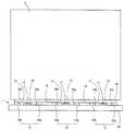
図1は、実施例1の線状光源装置1の構成を示した断面図、図2は斜視図である。図1、2のように、実施例1の線状光源装置1は、細長い長方形状の配線基板10と、配線基板10上に直線状に配置された発光素子11と、各発光素子毎に配線基板10上に配置されたリフレクタ12と、発光素子11を封止する封止樹脂13と、リフレクタ12上に配置された蛍光体板14と、によって構成されている。 FIG. 1 is a cross-sectional view illustrating the configuration of the linear light source device 1 according to the first embodiment, and FIG. 2 is a perspective view. As shown in FIGS. 1 and 2, the linear light source device 1 according to the first embodiment includes an elongated
配線基板10は、FR−5基板であり、ガラス布基材エポキシ樹脂からなる。他にもFR−4基板なども用いることができる。配線基板10の表面には、配線パターンが形成されており、その配線パターンと発光素子11とがボンディングワイヤ(図示しない)を介して接続されている。配線基板10は、細長い長方形状である。 The
発光素子11は、青色発光のIII 族窒化物半導体からなるフェイスアップ型のLEDである。発光素子11は、配線基板10上に、配線基板10の長手方向に沿って直線状に複数配置されている。また、配線基板10の配線パターンと発光素子11のn電極、p電極(いずれも図示しない)とが、ボンディングワイヤ(図示しない)を介して接続されている。 The
なお、実施例1では発光素子11をフェイスアップ型として配線基板10にワイヤボンディングしているが、発光素子11はフリップチップ型や縦方向に導通をとる構造のものを用いてもよい。 In Example 1, the light-emitting
リフレクタ12は、配線基板10上に、各発光素子11ごとに溝15によって分離されて設けられている。リフレクタ12は、たとえばポリフタルアミド、液晶ポリマ、エポキシ樹脂、変性エポキシ樹脂、シリコーン樹脂、変性シリコーン樹脂などの樹脂材料からなる。リフレクタ12は、線状光源装置1の長手方向において発光素子11を挟んで対向する2つの部分12a、bからなり、それぞれの部分12a、bは、発光素子11側に配線基板10の主面に対して傾斜した傾斜面16a、bを有している。傾斜面16a、bは、発光素子11上方側を上に見て逆ハの字型となるような傾斜角度を有している。この傾斜面16a、bによって発光素子11からの光を上方に反射させることによって、線状光源装置1の輝度を高めるとともに輝度のムラを低減している。 The
封止樹脂13は、透明なシリコーン樹脂からなり、発光素子11を封止するよう形成されている。封止樹脂13として他にもエポキシ樹脂、変性エポキシ樹脂、変性シリコーン樹脂などを用いることができる。この封止樹脂13は、発光素子11およびボンディングワイヤを保護するためのものである。また、封止樹脂13は、リフレクタ12に接触しないように形成されていて、全体として半円柱状である。封止樹脂13は、粘性を有したシリコーン樹脂をポッティングしたのち、熱処理して硬化させることにより形成する。この熱処理に際して、シリコーン樹脂は収縮するため、配線基板10に、配線基板10の発光素子11実装側から裏面側に向かって凸状に湾曲させるような応力を発生させる。 The sealing
なお、封止樹脂13は必ずしも透明である必要はなく、蛍光体や反射材などが混合されていてもよいが、線状光源装置1の色むらを抑制することができるので透明とすることが望ましい。 The sealing
蛍光体板14は、青色光によって励起されて黄色の蛍光を発する黄色蛍光体が混合されたガラスからなる。ガラスの他に、アクリル樹脂やエポキシ樹脂、変性エポキシ樹脂、シリコーン樹脂、変性シリコーン樹脂などの樹脂材料を用いてもよい。蛍光体板14は各リフレクタ12上に接着剤や両面テープなどによって接着されて配置されていて、すべての発光素子11の上部に位置している。また、発光素子11の上部において、封止樹脂13と蛍光体板14とは接触していない。そのため、配線基板10、リフレクタ12の傾斜面16a、b、封止樹脂13、蛍光体板14で囲まれた空間は空気層17となっている。 The
次に、線状光源装置1の動作について説明する。配線基板10の配線パターンを介して各発光素子11に電流が流れると、各発光素子11から青色光が放射状に出射し、一部は封止樹脂13、空気層17を介して蛍光体板14に達し、他の一部は封止樹脂13、空気層17を介してリフレクタ12の傾斜面16a、bに達し、傾斜面16a、bに反射されて蛍光体板14に達する。これにより発光素子11からの青色光は拡散し、各発光素子11が線状に配置されているため青色光も線状に拡散する。蛍光体板14に達した青色光は、一部はそのまま透過し、一部は蛍光体板14中の黄色蛍光体を励起して黄色光を発する。蛍光体板14を透過した青色光と、黄色蛍光体の励起による黄色光とが混色されて、線状光源装置1は、線状の白色光を発する。 Next, the operation of the linear light source device 1 will be described. When a current flows through each light emitting
この実施例1の線状光源装置1では、各リフレクタ12にまたがるようにして蛍光体板14を設けたことにより、封止樹脂13の熱収縮による配線基板10への応力が緩和され、線状光源装置1の湾曲を防止することができるとともに、線状光源装置1の色むらを抑制することができる。なお、このような理由から、蛍光体板14は、配線基板10よりも剛性が大きいことが望ましい。より線状光源装置1の湾曲を抑制することができる。剛性は、配線基板10および蛍光単板14の厚さや、材料の弾性率によって決まるため、これらを制御することで蛍光単板14の方が配線基板10よりも剛性が大きくなるようにすることができる。 In the linear light source device 1 according to the first embodiment, the
また、封止樹脂13は、リフレクタ12に接触せず、蛍光単板14にも接触していない。そのため、封止樹脂13の量が従来よりも少量で済み、封止樹脂13の熱収縮による応力が弱まるため、線状光源装置の湾曲をより抑制することができる。また、発光素子11上部において蛍光体板14と封止樹脂13とが空気層17を介して非接触の状態としたので、実施例1の線状光源装置1を導光板と組み合わせて面状光源装置とした場合に、導光板に熱が伝わりにくくなり、導光板の劣化を防止することができる。 Further, the sealing
図3は、実施例2の面状光源装置の構成を示した図である。実施例2の面状光源装置は、矩形の導光板2と、導光板2の側面に配置された実施例1の線状光源装置1とによって構成されている。線状光源装置1と導光板2は、導光板2の側面2aと、線状光源装置1の蛍光体板14とが接触するように枠体(図示しない)によって固定されている。また、線状光源装置1の蛍光体板14は、導光板2よりも屈折率の低い、もしくは同じ屈折率の材料を用いている。導光板2には、アクリル樹脂、ポリカーボネート樹脂などを用いることができる。 FIG. 3 is a diagram illustrating the configuration of the planar light source device according to the second embodiment. The planar light source device according to the second embodiment includes a rectangular
実施例2の面状光源装置では、湾曲の抑制された実施例1の線状光源装置1を用いているため、導光板2への光入射効率が高く、面状に高輝度に発光させることができる。また、実施例1の線状光源装置1において封止樹脂13と蛍光体板14との間に空気層17があるため、発光素子11の発する熱が導光板2へと伝導しにくく、導光板2の熱による劣化を抑制することができる。また、蛍光体板14の屈折率が導光板2の屈折率よりも低いため、蛍光体板14から導光板2への光入射効率が高く、より高輝度に面状発光させることができる。 In the planar light source device according to the second embodiment, since the linear light source device 1 according to the first embodiment in which bending is suppressed is used, the light incident efficiency to the
なお、実施例1の線状光源装置1では、発光素子11として青色光のLEDを用い、蛍光体板14に混合する蛍光体として黄色蛍光体を用い、線状光源装置1の発色光を白色とするものであったが、発光素子11の発光色および蛍光体の蛍光色はこれらに限るものではなく、任意の発光色と任意の蛍光色を組み合わせて任意の発光色を得るものであってよい。たとえば、発光素子として紫外発光LEDを用い、蛍光体板14に混合する蛍光体として赤色蛍光体、緑色蛍光体、青色蛍光体の3つを用いることで、線状光源装置1の発色光を白色とすることもできる。 In the linear light source device 1 of Example 1, a blue light LED is used as the
本発明の線状光源装置は、導光板と組み合わせて面状光源装置として、携帯電話やデジタルカメラなどの小型の液晶表示パネルのバックライト光源として利用することができる。 The linear light source device of the present invention can be used as a planar light source device in combination with a light guide plate as a backlight light source of a small liquid crystal display panel such as a mobile phone or a digital camera.
1:線状光源装置
2:導光板
10:配線基板
11:発光素子
12:リフレクタ
13:封止樹脂
14:蛍光体板
15:溝
16a、b:傾斜面
17:空気層1: Linear light source device 2: Light guide plate 10: Wiring substrate 11: Light emitting element 12: Reflector 13: Sealing resin 14: Phosphor plate 15:
Claims (6)
Translated fromJapaneseすべての前記発光素子上部に位置するよう、各前記リフレクタ上にまたがるようにして、各前記リフレクタと接触させて配置された蛍光体板を有し、
各前記発光素子上部において前記蛍光体板と前記封止樹脂とが空気層を介することで非接触であり、
前記配線基板と前記リフレクタは異なる材料からなり、
前記蛍光体板は、剛性が前記配線基板よりも大きい、
ことを特徴とする線状光源装置。A wiring board on which a wiring pattern is formed in a rectangular shape, and said a plurality of linearly arranged along the longitudinal direction of the wiring board on a wiring substrate, the light emitting element connected to the wiring pattern of the wiringboard, the shorter The light emitting elements are separated from each other by a groove extending in the direction, and are composed of a first part and a second part that are opposed to each other with the light emitting element sandwiched in the longitudinal direction. The first part and the second part In the linear light source devicehaving a plurality of reflectorshaving inclined surfaces on the light emitting element side and a sealing resin for sealing each light emitting element,
A phosphor plate disposed onand in contact with each reflector so as to be positioned above all the light emitting elements;
And the phosphor plate at each of said light-emitting element portion and the sealing resin isRi contactless der in passing through the airlayer,
The wiring board and the reflector are made of different materials,
The phosphor plate is larger in rigidity than the wiring board,
A linear light source device.
前記線状光源装置は、前記導光板の側面と、前記線状光源装置の前記蛍光体板が接触するよう配置され、
前記蛍光体板の屈折率は、前記導光板の屈折率以下である、
ことを特徴とする面状光源装置。
In the planar light source device having the light guide plate and the linear light source device according to claim 1 disposed with the light emitting surface facing the side surface of the light guide plate,
The linear light source device is arranged such that a side surface of the light guide plate and the phosphor plate of the linear light source device are in contact with each other,
The refractive index of the phosphor plate is equal to or lower than the refractive index of the light guide plate.
A planar light source device.
Priority Applications (2)
| Application Number | Priority Date | Filing Date | Title |
|---|---|---|---|
| JP2011205196AJP5533827B2 (en) | 2011-09-20 | 2011-09-20 | Linear light source device |
| US13/607,238US20130070481A1 (en) | 2011-09-20 | 2012-09-07 | Linear light source apparatus |
Applications Claiming Priority (1)
| Application Number | Priority Date | Filing Date | Title |
|---|---|---|---|
| JP2011205196AJP5533827B2 (en) | 2011-09-20 | 2011-09-20 | Linear light source device |
Publications (2)
| Publication Number | Publication Date |
|---|---|
| JP2013069424A JP2013069424A (en) | 2013-04-18 |
| JP5533827B2true JP5533827B2 (en) | 2014-06-25 |
Family
ID=47880520
Family Applications (1)
| Application Number | Title | Priority Date | Filing Date |
|---|---|---|---|
| JP2011205196AExpired - Fee RelatedJP5533827B2 (en) | 2011-09-20 | 2011-09-20 | Linear light source device |
Country Status (2)
| Country | Link |
|---|---|
| US (1) | US20130070481A1 (en) |
| JP (1) | JP5533827B2 (en) |
Families Citing this family (4)
| Publication number | Priority date | Publication date | Assignee | Title |
|---|---|---|---|---|
| JP5479634B1 (en)* | 2013-05-08 | 2014-04-23 | 久豊技研株式会社 | Light emitting device |
| JP6765804B2 (en)* | 2014-11-28 | 2020-10-07 | エルジー イノテック カンパニー リミテッド | Light emitting element package |
| CN104570499B (en)* | 2014-12-30 | 2018-01-09 | 深圳市华星光电技术有限公司 | Liquid crystal panel and its manufacture method and liquid crystal display device |
| WO2017163598A1 (en)* | 2016-03-24 | 2017-09-28 | ソニー株式会社 | Light emitting device, display apparatus, and illumination apparatus |
Family Cites Families (35)
| Publication number | Priority date | Publication date | Assignee | Title |
|---|---|---|---|---|
| JPH0546288Y2 (en)* | 1987-09-11 | 1993-12-03 | ||
| JP3187280B2 (en)* | 1995-05-23 | 2001-07-11 | シャープ株式会社 | Surface lighting device |
| JP2002042525A (en)* | 2000-07-26 | 2002-02-08 | Toyoda Gosei Co Ltd | Planar light source |
| AT410266B (en)* | 2000-12-28 | 2003-03-25 | Tridonic Optoelectronics Gmbh | LIGHT SOURCE WITH A LIGHT-EMITTING ELEMENT |
| US6737681B2 (en)* | 2001-08-22 | 2004-05-18 | Nichia Corporation | Light emitting device with fluorescent member excited by semiconductor light emitting element |
| JPWO2003034508A1 (en)* | 2001-10-12 | 2005-02-03 | 日亜化学工業株式会社 | Light emitting device and manufacturing method thereof |
| KR20040092512A (en)* | 2003-04-24 | 2004-11-04 | (주)그래픽테크노재팬 | A semiconductor light emitting device with reflectors having a cooling function |
| CN100466308C (en)* | 2003-09-29 | 2009-03-04 | 松下电器产业株式会社 | Line light source device, manufacturing method thereof, and surface light emitting device |
| US7315119B2 (en)* | 2004-05-07 | 2008-01-01 | Avago Technologies Ip (Singapore) Pte Ltd | Light-emitting device having a phosphor particle layer with specific thickness |
| JP2006120691A (en)* | 2004-10-19 | 2006-05-11 | Matsushita Electric Ind Co Ltd | Linear light source device |
| KR101114305B1 (en)* | 2004-12-24 | 2012-03-08 | 쿄세라 코포레이션 | Light-emitting device and illuminating device |
| US20090052157A1 (en)* | 2005-02-24 | 2009-02-26 | Kyocera Corporation | Light emitting device and lighting apparatus |
| US7350933B2 (en)* | 2005-05-23 | 2008-04-01 | Avago Technologies Ecbu Ip Pte Ltd | Phosphor converted light source |
| JP2007036044A (en)* | 2005-07-28 | 2007-02-08 | Mitsubishi Rayon Co Ltd | Surface light source device |
| KR100826401B1 (en)* | 2005-12-02 | 2008-05-02 | 삼성전기주식회사 | LED backlight unit |
| JP4417906B2 (en)* | 2005-12-16 | 2010-02-17 | 株式会社東芝 | Light emitting device and manufacturing method thereof |
| KR100771772B1 (en)* | 2006-08-25 | 2007-10-30 | 삼성전기주식회사 | White LED Module |
| US20080117619A1 (en)* | 2006-11-21 | 2008-05-22 | Siew It Pang | Light source utilizing a flexible circuit carrier and flexible reflectors |
| KR100946015B1 (en)* | 2007-01-02 | 2010-03-09 | 삼성전기주식회사 | White light emitting device and light source module for LCD backlight using the same |
| EP2120271A4 (en)* | 2007-03-01 | 2015-03-25 | Nec Lighting Ltd | LED ARRANGEMENT AND LIGHTING DEVICE |
| US20100110728A1 (en)* | 2007-03-19 | 2010-05-06 | Nanosys, Inc. | Light-emitting diode (led) devices comprising nanocrystals |
| KR101283129B1 (en)* | 2007-04-03 | 2013-07-05 | 엘지이노텍 주식회사 | Light guide plate, surface light source apparatus and display apparatus having thereof |
| CN101315484B (en)* | 2007-06-01 | 2011-09-28 | 富士迈半导体精密工业(上海)有限公司 | Light source component and back light module unit including the same |
| TW200909931A (en)* | 2007-08-22 | 2009-03-01 | Nano Prec Corp | Backlight module and liquid crystal display using the same |
| EP2237331B1 (en)* | 2007-12-26 | 2017-01-25 | Kyocera Corporation | Light-emitting device and illuminating device |
| CN101493216B (en)* | 2008-01-24 | 2011-11-09 | 富士迈半导体精密工业(上海)有限公司 | LED light source module |
| US7988311B2 (en)* | 2008-06-30 | 2011-08-02 | Bridgelux, Inc. | Light emitting device having a phosphor layer |
| US7994529B2 (en)* | 2008-11-05 | 2011-08-09 | Koninklijke Philips Electronics N.V. | LED with molded bi-directional optics |
| KR101629654B1 (en)* | 2008-12-19 | 2016-06-13 | 삼성전자주식회사 | Light emitting device package, backlight unit, display device and illumination device |
| JP2010147305A (en)* | 2008-12-19 | 2010-07-01 | Toyoda Gosei Co Ltd | Light-emitting device and light source device |
| JP2011060678A (en)* | 2009-09-14 | 2011-03-24 | Rohm Co Ltd | Led lighting system and liquid crystal display device |
| EP2312346B1 (en)* | 2009-10-19 | 2013-03-20 | LG Innotek Co., Ltd. | Optical film and a method for fabricating the same |
| KR101208174B1 (en)* | 2010-07-28 | 2012-12-04 | 엘지이노텍 주식회사 | Optical sheet and light emitting device comprising the same |
| JP2012039031A (en)* | 2010-08-11 | 2012-02-23 | Nitto Denko Corp | Light emitting device |
| US20120281387A1 (en)* | 2011-05-04 | 2012-11-08 | Ligitek Electronics Co., Ltd. | Structure of light-emitting diode |
- 2011
- 2011-09-20JPJP2011205196Apatent/JP5533827B2/ennot_activeExpired - Fee Related
- 2012
- 2012-09-07USUS13/607,238patent/US20130070481A1/ennot_activeAbandoned
Also Published As
| Publication number | Publication date |
|---|---|
| JP2013069424A (en) | 2013-04-18 |
| US20130070481A1 (en) | 2013-03-21 |
Similar Documents
| Publication | Publication Date | Title |
|---|---|---|
| JP5533830B2 (en) | Linear light source device | |
| JP7125636B2 (en) | light emitting device | |
| JP5545279B2 (en) | Surface light source device | |
| JP6658723B2 (en) | Light emitting device | |
| JP6339161B2 (en) | Light emitting device package | |
| US8450929B2 (en) | Light emitting device, backlight unit, liquid crystal display apparatus, and lighting apparatus | |
| CN108242442A (en) | light emitting device | |
| JP6399017B2 (en) | Light emitting device | |
| JP5716623B2 (en) | Linear light source device and planar light source device | |
| US20100188601A1 (en) | Light emitting diode backlight unit and liquid crystal display device having the same | |
| JP2007036073A (en) | LIGHTING DEVICE AND DISPLAY DEVICE USING THE LIGHTING DEVICE | |
| JP2013042095A (en) | Semiconductor light emitting device | |
| JP6303880B2 (en) | Backlight device | |
| KR20120064524A (en) | Led package and lcd module including the same | |
| JP5533827B2 (en) | Linear light source device | |
| CN110828637A (en) | Light emitting diode package and display device provided with light emitting diode package | |
| KR101055037B1 (en) | Light unit and display device having same | |
| JP2011176234A (en) | Semiconductor light emitting device | |
| KR20110107631A (en) | Light emitting device package and light unit having same | |
| WO2013114977A1 (en) | Linear light source device, surface light-emitting device, and liquid crystal display device | |
| JP2006120691A (en) | Linear light source device | |
| JP4594859B2 (en) | LIGHTING DEVICE AND IMAGE DISPLAY DEVICE USING THE SAME | |
| JP2020053617A (en) | Light emitting device | |
| KR102198695B1 (en) | Light source module and backlight unit having the same | |
| JP2016072076A (en) | Backlight device |
Legal Events
| Date | Code | Title | Description |
|---|---|---|---|
| A621 | Written request for application examination | Free format text:JAPANESE INTERMEDIATE CODE: A621 Effective date:20130918 | |
| A977 | Report on retrieval | Free format text:JAPANESE INTERMEDIATE CODE: A971007 Effective date:20131226 | |
| A131 | Notification of reasons for refusal | Free format text:JAPANESE INTERMEDIATE CODE: A131 Effective date:20140107 | |
| A521 | Request for written amendment filed | Free format text:JAPANESE INTERMEDIATE CODE: A523 Effective date:20140306 | |
| TRDD | Decision of grant or rejection written | ||
| A01 | Written decision to grant a patent or to grant a registration (utility model) | Free format text:JAPANESE INTERMEDIATE CODE: A01 Effective date:20140401 | |
| R150 | Certificate of patent or registration of utility model | Ref document number:5533827 Country of ref document:JP Free format text:JAPANESE INTERMEDIATE CODE: R150 | |
| A61 | First payment of annual fees (during grant procedure) | Free format text:JAPANESE INTERMEDIATE CODE: A61 Effective date:20140414 | |
| LAPS | Cancellation because of no payment of annual fees |