JP5532301B2 - Driving circuit and display device - Google Patents
Driving circuit and display deviceDownload PDFInfo
- Publication number
- JP5532301B2 JP5532301B2JP2009295552AJP2009295552AJP5532301B2JP 5532301 B2JP5532301 B2JP 5532301B2JP 2009295552 AJP2009295552 AJP 2009295552AJP 2009295552 AJP2009295552 AJP 2009295552AJP 5532301 B2JP5532301 B2JP 5532301B2
- Authority
- JP
- Japan
- Prior art keywords
- transistor
- source
- voltage
- circuit
- drain
- Prior art date
- Legal status (The legal status is an assumption and is not a legal conclusion. Google has not performed a legal analysis and makes no representation as to the accuracy of the status listed.)
- Active
Links
Images


Classifications
- G—PHYSICS
- G09—EDUCATION; CRYPTOGRAPHY; DISPLAY; ADVERTISING; SEALS
- G09G—ARRANGEMENTS OR CIRCUITS FOR CONTROL OF INDICATING DEVICES USING STATIC MEANS TO PRESENT VARIABLE INFORMATION
- G09G3/00—Control arrangements or circuits, of interest only in connection with visual indicators other than cathode-ray tubes
- G09G3/20—Control arrangements or circuits, of interest only in connection with visual indicators other than cathode-ray tubes for presentation of an assembly of a number of characters, e.g. a page, by composing the assembly by combination of individual elements arranged in a matrix no fixed position being assigned to or needed to be assigned to the individual characters or partial characters
- G09G3/22—Control arrangements or circuits, of interest only in connection with visual indicators other than cathode-ray tubes for presentation of an assembly of a number of characters, e.g. a page, by composing the assembly by combination of individual elements arranged in a matrix no fixed position being assigned to or needed to be assigned to the individual characters or partial characters using controlled light sources
- G09G3/30—Control arrangements or circuits, of interest only in connection with visual indicators other than cathode-ray tubes for presentation of an assembly of a number of characters, e.g. a page, by composing the assembly by combination of individual elements arranged in a matrix no fixed position being assigned to or needed to be assigned to the individual characters or partial characters using controlled light sources using electroluminescent panels
- G09G3/32—Control arrangements or circuits, of interest only in connection with visual indicators other than cathode-ray tubes for presentation of an assembly of a number of characters, e.g. a page, by composing the assembly by combination of individual elements arranged in a matrix no fixed position being assigned to or needed to be assigned to the individual characters or partial characters using controlled light sources using electroluminescent panels semiconductive, e.g. using light-emitting diodes [LED]
- G09G3/3208—Control arrangements or circuits, of interest only in connection with visual indicators other than cathode-ray tubes for presentation of an assembly of a number of characters, e.g. a page, by composing the assembly by combination of individual elements arranged in a matrix no fixed position being assigned to or needed to be assigned to the individual characters or partial characters using controlled light sources using electroluminescent panels semiconductive, e.g. using light-emitting diodes [LED] organic, e.g. using organic light-emitting diodes [OLED]
- G09G3/3225—Control arrangements or circuits, of interest only in connection with visual indicators other than cathode-ray tubes for presentation of an assembly of a number of characters, e.g. a page, by composing the assembly by combination of individual elements arranged in a matrix no fixed position being assigned to or needed to be assigned to the individual characters or partial characters using controlled light sources using electroluminescent panels semiconductive, e.g. using light-emitting diodes [LED] organic, e.g. using organic light-emitting diodes [OLED] using an active matrix
- G09G3/3233—Control arrangements or circuits, of interest only in connection with visual indicators other than cathode-ray tubes for presentation of an assembly of a number of characters, e.g. a page, by composing the assembly by combination of individual elements arranged in a matrix no fixed position being assigned to or needed to be assigned to the individual characters or partial characters using controlled light sources using electroluminescent panels semiconductive, e.g. using light-emitting diodes [LED] organic, e.g. using organic light-emitting diodes [OLED] using an active matrix with pixel circuitry controlling the current through the light-emitting element
- G—PHYSICS
- G09—EDUCATION; CRYPTOGRAPHY; DISPLAY; ADVERTISING; SEALS
- G09G—ARRANGEMENTS OR CIRCUITS FOR CONTROL OF INDICATING DEVICES USING STATIC MEANS TO PRESENT VARIABLE INFORMATION
- G09G2300/00—Aspects of the constitution of display devices
- G09G2300/04—Structural and physical details of display devices
- G09G2300/0421—Structural details of the set of electrodes
- G09G2300/043—Compensation electrodes or other additional electrodes in matrix displays related to distortions or compensation signals, e.g. for modifying TFT threshold voltage in column driver
- G—PHYSICS
- G09—EDUCATION; CRYPTOGRAPHY; DISPLAY; ADVERTISING; SEALS
- G09G—ARRANGEMENTS OR CIRCUITS FOR CONTROL OF INDICATING DEVICES USING STATIC MEANS TO PRESENT VARIABLE INFORMATION
- G09G2320/00—Control of display operating conditions
- G09G2320/04—Maintaining the quality of display appearance
- G09G2320/043—Preventing or counteracting the effects of ageing
Landscapes
- Engineering & Computer Science (AREA)
- Physics & Mathematics (AREA)
- Computer Hardware Design (AREA)
- General Physics & Mathematics (AREA)
- Theoretical Computer Science (AREA)
- Control Of El Displays (AREA)
- Control Of Indicators Other Than Cathode Ray Tubes (AREA)
- Electroluminescent Light Sources (AREA)
- Electronic Switches (AREA)
Description
Translated fromJapanese本発明は、例えば有機EL(Electro Luminescence)素子を用いた表示装置に好適に適用可能な駆動回路に関する。また、本発明は、上記駆動回路を備えた表示装置に関する。 The present invention relates to a drive circuit that can be suitably applied to a display device using, for example, an organic EL (Electro Luminescence) element. The present invention also relates to a display device provided with the above drive circuit.
近年、画像表示を行う表示装置の分野では、画素の発光素子として、流れる電流値に応じて発光輝度が変化する電流駆動型の光学素子、例えば有機EL素子を用いた表示装置が開発され、商品化が進められている。有機EL素子は、液晶素子などと異なり自発光素子である。そのため、有機EL素子を用いた表示装置(有機EL表示装置)では、有機EL素子に流れる電流値を制御することで、発色の階調が得られる。 In recent years, in the field of display devices that perform image display, display devices using current-driven optical elements, such as organic EL elements, whose light emission luminance changes according to the value of a flowing current have been developed as light-emitting elements of pixels. Is being promoted. Unlike a liquid crystal element or the like, the organic EL element is a self-luminous element. Therefore, in a display device (organic EL display device) using an organic EL element, a gradation of color can be obtained by controlling a current value flowing through the organic EL element.
有機EL表示装置では、液晶表示装置と同様、その駆動方式として単純(パッシブ)マトリクス方式とアクティブマトリクス方式とがある。前者は、構造が単純であるものの、大型かつ高精細の表示装置の実現が難しいなどの問題がある。そのため、現在では、アクティブマトリクス方式の開発が盛んに行なわれている。この方式は、画素ごとに配した発光素子に流れる電流を駆動トランジスタによって制御するものである。 In the organic EL display device, similarly to the liquid crystal display device, there are a simple (passive) matrix method and an active matrix method as its driving method. Although the former has a simple structure, there is a problem that it is difficult to realize a large-sized and high-definition display device. For this reason, active matrix systems are currently being actively developed. In this method, a current flowing through a light emitting element arranged for each pixel is controlled by a driving transistor.
上記の駆動トランジスタでは、閾値電圧Vthや移動度μが経時的に変化したり、製造プロセスのばらつきによって閾値電圧Vthや移動度μが画素ごとに異なったりする場合がある。閾値電圧Vthや移動度μが画素ごとに異なる場合には、駆動トランジスタに流れる電流値が画素ごとにばらつくので、駆動トランジスタのゲートに同じ電圧を印加しても、有機EL素子の発光輝度がばらつき、画面の一様性(ユニフォーミティ)が損なわれる。そこで、閾値電圧Vthや移動度μの変動に対する補正機能を組み込んだ表示装置が開発されている(例えば、特許文献1参照)。In the drive transistor described above, the threshold voltage Vth and the mobility μ may change over time, or the threshold voltage Vth and the mobility μ may vary from pixel to pixel due to manufacturing process variations. When the threshold voltage Vth and the mobility μ are different for each pixel, the value of the current flowing through the driving transistor varies from pixel to pixel. Therefore, even if the same voltage is applied to the gate of the driving transistor, the light emission luminance of the organic EL element is Variation and uniformity of the screen are lost. In view of this, a display device incorporating a correction function for variations in threshold voltage Vth and mobility μ has been developed (see, for example, Patent Document 1).
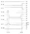
閾値電圧Vthや移動度μの変動に対する補正は、画素ごとに配した画素回路によって行われる。この画素回路は、例えば、図20に示したように、有機EL素子111に流れる電流を制御する駆動トランジスタTr1と、信号線DTLの電圧を駆動トランジスタTr1に書き込む書き込みトランジスタTr2と、保持容量Csとによって構成されており、2Tr1Cの回路構成となっている。駆動トランジスタTr1および書き込みトランジスタTr2は、例えば、nチャネルMOS型の薄膜トランジスタ(TFT(Thin Film Transistor))により形成されている。Correction for variations in threshold voltage Vth and mobility μ is performed by a pixel circuit arranged for each pixel. For example, as shown in FIG. 20, the pixel circuit includes a drive transistor Tr1 that controls a current flowing through the
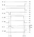
図19は、画素回路に印加される電圧波形の一例と、駆動トランジスタのゲート電圧およびソース電圧の変化の一例とを表したものである。図19(A)には信号線DTLに、信号電圧Vsigと、オフセット電圧Vofsが印加されている様子が示されている。図19(B)には書込線WSLに、駆動トランジスタをオンする電圧Vddと、駆動トランジスタをオフする電圧Vssが印加されている様子が示されている。図19(C)には電源線PSLに、ハイ電圧VccHと、ロー電圧VccLが印加されている様子が示されている。さらに、図19(D),(E)には、電源線PSL、信号線DTLおよび書込線WSLへの電圧印加に応じて、駆動トランジスタTr1のゲート電圧Vgおよびソース電圧Vsが時々刻々変化している様子が示されている。FIG. 19 shows an example of a voltage waveform applied to the pixel circuit and an example of changes in the gate voltage and source voltage of the driving transistor. FIG. 19A shows a state in which the signal voltage Vsig and the offset voltage Vofs are applied to the signal line DTL. FIG. 19B shows a state where a voltage Vdd for turning on the driving transistor and a voltage Vss for turning off the driving transistor are applied to the writing line WSL. FIG.19C shows a state where the high voltage VccH and the low voltage VccL are applied to the power supply line PSL. Further, in FIGS. 19D and 19E, the gate voltage Vg and the source voltage Vs of the drive transistor Tr1 are sometimes changed according to the voltage application to the power supply line PSL, the signal line DTL, and the write line WSL. It shows how it changes every moment.
図19から、1H内に2回、WSパルスP1が書込線WSLに印加されており、1回目のWSパルスP1によって閾値補正が行われ、2回目のWSパルスP1によって移動度補正と信号書き込みが行われていることがわかる。つまり、図19において、WSパルスP1は、信号書込みだけでなく、駆動トランジスタTr1の閾値補正や移動度補正にも用いられている。From FIG. 19, the WS pulse P1 is applied to the write line WSL twice within 1H, threshold correction is performed by the first WS pulse P1, and mobility correction and signal writing are performed by the second WS pulse P1. Can be seen. That is, inFIG. 19, WS pulse P1 is not only the signal writing is also used in the threshold correction and the mobility correction of the driving transistor Tr1.
以下、駆動トランジスタTr1の閾値補正および移動度補正について説明する。2回目のWSパルスP1の印加により、信号電圧Vsigが駆動トランジスタTr1のゲートに書き込まれる。これにより、駆動トランジスタTr1がオンし、駆動トランジスタTr1に電流が流れる。このとき、有機EL素子111に逆バイアスが印加されているとすると、駆動トランジスタTr1から流れ出た電荷は、保持容量Csおよび有機EL素子111の素子容量(図示せず)に充電され、ソース電圧Vsが上昇する。駆動トランジスタTr1の移動度が高い場合には、駆動トランジスタTr1に流れる電流が大きくなるので、ソース電圧Vsの上昇が早くなる。逆に、駆動トランジスタTr1の移動度が低い場合には、駆動トランジスタTr1に流れる電流が小さくなるので、駆動トランジスタTr1の移動度が高い場合と比べて、ソース電圧Vsの上昇が遅くなる。従って、移動度を補正する期間を調整することにより、移動度を補正することができる。Hereinafter, threshold correction and mobility correction of the drive transistor Tr1 will be described. By applying the WS pulse P1 for the second time, the signal voltage Vsig is written to the gate of the driving transistor Tr1 . As a result, the drive transistor Tr1 is turned on, and a current flows through the drive transistor Tr1 . At this time,assuming that a reverse bias is applied to the
ところで、アクティブマトリクス方式の表示装置では、信号線を駆動する水平駆動回路や、各画素を順次選択する書き込み走査回路は、いずれも基本的にシフトレジスタ(図示せず)を含んで構成されており、画素の各列または各行に対応して、1段ごとにバッファ回路を備えている。例えば、走査回路内のバッファ回路は、典型的には、図21に示したように、2つのインバータ回路210,220を直列に接続して構成されている。図21のバッファ回路200において、インバータ回路210は、pチャネル型のMOSトランジスタおよびnチャネル型のMOSトランジスタが並列接続された回路構成となっている。一方、インバータ回路220は、CMOSトランジスタおよびnチャネル型のMOSトランジスタが並列接続された回路構成となっている。バッファ回路200は、ハイレベルの電圧が印加される高電圧配線LHと、ローレベルの電圧が印加される低電圧配線LLとの間に挿入されている。By the way, in an active matrix display device, a horizontal drive circuit that drives signal lines and a write scanning circuit that sequentially selects each pixel basically include a shift register (not shown). A buffer circuit is provided for each stage corresponding to each column or each row of pixels. For example, the buffer circuit in the scanning circuit is typically configured by connecting two
しかし、CMOSトランジスタにおいて、例えば、図22に示したように、pチャネル型のMOSトランジスタの閾値電圧Vth1がΔVth1だけばらつくと、出力OUTの電圧Voutの立ち上がるタイミングがΔt1だけずれる。また、CMOSトランジスタにおいて、例えば、図23に示したように、nチャネル型のMOSトランジスタの閾値電圧Vth2がΔVth2だけばらつくと、出力OUTの電圧Voutの立ち上るタイミングがΔt2だけずれる。従って、例えば、出力OUTの電圧Voutの立ち上がるタイミングがばらつき、移動度補正期間ΔTがΔt1またはΔt2だけばらついた場合には、例えば、図24に示したように、発光時の電流IdsがΔIdsだけばらつき、そのばらつきが輝度のばらつきとなってしまうという問題があった。なお、図24は、移動度補正期間ΔTと、発光輝度との関係の一例を表したものである。However, in the CMOS transistor, for example, as shown in FIG. 22, when the threshold voltage Vth1 of the p-channel MOS transistor varies by ΔVth1 , the rising timing of the voltage Vout of the output OUT is shifted by Δt1 . Further, in the CMOS transistor, for example, as shown in FIG. 23, when the threshold voltage Vth2 of the n-channel MOS transistor varies by ΔVth2 , the rise timing of the voltage Vout of the output OUT is shifted by Δt2 . Thus, for example, variations rising timing of the voltage Vout ofthe output OUT, when the mobility correction period ΔT is varied by Delta] t1 or Delta] t2, for example, as shown in FIG. 24, upon light emission current Ids However, there is a problem that the variation is ΔIds , and the variation is luminance variation. FIG. 24 shows an example of the relationship between the mobility correction period ΔT and the light emission luminance.
なお、閾値電圧Vthのばらつきの問題は、表示装置の走査回路に限って生じるものではなく、他のデバイスにおいても同様に生じ得るものである。Note that the problem of variation in the threshold voltage Vth does not occur only in the scanning circuit of the display device, but can occur in other devices as well.
本発明はかかる問題点に鑑みてなされたものであり、その目的は、出力電圧の立ち上がるタイミングのばらつきを低減することの可能な駆動回路、およびこの駆動回路を備えた表示装置を提供することにある。 The present invention has been made in view of such problems, and an object of the present invention is to provide a drive circuit capable of reducing variations in the rise timing of the output voltage, and a display device including the drive circuit. is there.
本発明の駆動回路は、互いに直列に接続されると共に高電圧線および低電圧線の間に挿入された入力側インバータ回路および出力側インバータ回路を備えている。出力側インバータ回路は、CMOSトランジスタと、MOSトランジスタとを備えている。CMOSトランジスタにおいては、ドレインが高電圧線側に接続されると共にソースが当該出力側インバータ回路の出力側に接続されており、かつドレイン同士が互いに接続されると共にソース同士が互いに接続されている。MOSトランジスタにおいては、ドレインが低電圧線側に接続され、ソースが当該出力側インバータ回路の出力側に接続されている。この出力側インバータ回路は、さらに、補正回路を有している。補正回路は、第1トランジスタと、第2トランジスタと、第3トランジスタと、第1容量素子とを有している。第1トランジスタでは、ソースまたはドレインがCMOSトランジスタの第1ゲート側に接続され、かつソースおよびドレインのうちCMOSトランジスタの第1ゲート側に未接続の方が高電圧線側に接続されている。第2トランジスタでは、ソースまたはドレインがCMOSトランジスタの第1ゲート側に接続され、かつソースおよびドレインのうちCMOSトランジスタの第1ゲート側に未接続の方がCMOSトランジスタのドレイン側に接続されている。第3トランジスタでは、ソースまたはドレインがCMOSトランジスタのドレイン側に接続され、かつソースおよびドレインのうちCMOSトランジスタのドレイン側に未接続の方が高電圧線側に接続されている。第1容量素子では、一方がCMOSトランジスタの第1ゲート側に接続され、かつ他方が入力側インバータ回路の入力側に接続されている。補正回路は、CMOSトランジスタの第1ゲート側のトランジスタがオフしているときに、CMOSトランジスタの第1ゲートに対して、CMOSトランジスタの閾値電圧に対応する電圧をオフセットとして設定する。The drive circuit of the present invention includes an input side inverter circuit and an output side inverter circuit that are connected in series with each other and inserted between a high voltage line and a low voltage line. The output side inverter circuit includes a CMOS transistor and a MOS transistor. In the CMOS transistor, the drain is connected to the high voltage line side, the source is connected to the output side of the output side inverter circuit, the drains are connected to each other, and the sources are connected to each other. In the MOS transistor, the drain is connected to the low voltage line side, and the source is connected to the output side of the output side inverter circuit. This output-side inverter circuit furtherincludes a correction circuit .The correction circuit includes a first transistor, a second transistor, a third transistor, and a first capacitor element. In the first transistor, the source or drain is connected to the first gate side of the CMOS transistor, and the source and drain that are not connected to the first gate side of the CMOS transistor are connected to the high voltage line side. In the second transistor, the source or drain is connected to the first gate side of the CMOS transistor, and the source and drain that are not connected to the first gate side of the CMOS transistor are connected to the drain side of the CMOS transistor. In the third transistor, the source or drain is connected to the drain side of the CMOS transistor, and the source or drain of the third transistor that is not connected to the drain side of the CMOS transistor is connected to the high voltage line side. In the first capacitive element, one is connected to the first gate side of the CMOS transistor and the other is connected to the input side of the input side inverter circuit. The correction circuit sets a voltage corresponding to the threshold voltage of the CMOS transistor as an offset with respect to the first gate of the CMOS transistor when the transistor on the first gate side of the CMOS transistor is off.
本発明の表示装置は、行状に配置された複数の走査線と、列状に配置された複数の信号線と、行列状に配置された複数の画素とを含む表示部を備えており、さらに、各画素を駆動する駆動部を備えている。駆動部は、走査線ごとに1つずつ設けられた複数の駆動回路を有しており、駆動部内の各駆動回路は、上記の駆動回路と同一の構成要素を含んでいる。 The display device of the present invention includes a display unit including a plurality of scanning lines arranged in rows, a plurality of signal lines arranged in columns, and a plurality of pixels arranged in a matrix, And a driving unit for driving each pixel. The drive unit includes a plurality of drive circuits provided for each scanning line, and each drive circuit in the drive unit includes the same components as the above drive circuit.
本発明の駆動回路および表示装置では、互いに直列に接続された入力側インバータ回路および出力側インバータ回路のうち出力側インバータ回路に、CMOSトランジスタの2つのゲートの少なくとも一方の電圧の補正を行う補正回路が組み込まれている。これにより、CMOSトランジスタの2つのゲートの少なくとも一方に対して、CMOSトランジスタの閾値電圧に対応する電圧をオフセットとして設定することができる。 In the drive circuit and the display device of the present invention, the correction circuit that corrects the voltage of at least one of the two gates of the CMOS transistor on the output-side inverter circuit of the input-side inverter circuit and the output-side inverter circuit connected in series with each other. Is incorporated. Thus, a voltage corresponding to the threshold voltage of the CMOS transistor can be set as an offset for at least one of the two gates of the CMOS transistor.
本発明の駆動回路および表示装置によれば、CMOSトランジスタの2つのゲートの少なくとも一方に対して、CMOSトランジスタの閾値電圧に対応する電圧をオフセットとして設定することができるようにした。これにより、駆動回路の出力電圧が立ち上がるタイミングにおいて、ばらつきを低減することができる。従って、例えば、有機EL表示装置においては、発光時に有機EL素子に流れる電流のばらつきを低減することができるので、輝度の均一性を向上させることができる。 According to the driving circuit and the display device of the present invention, a voltage corresponding to the threshold voltage of the CMOS transistor can be set as an offset for at least one of the two gates of the CMOS transistor. Thereby, the variation can be reduced at the timing when the output voltage of the drive circuit rises. Therefore, for example, in an organic EL display device, variation in current flowing through the organic EL element during light emission can be reduced, so that uniformity of luminance can be improved.
以下、発明を実施するための形態について、図面を参照して詳細に説明する。なお、説明は以下の順序で行う。
1.第1の実施の形態(図1〜図4)
2.第2の実施の形態(図5〜図8)
3.第3の実施の形態(図9〜図12)
4.第4の実施の形態(図13〜図16)
5.適用例(図17〜図19)
6.従来技術の説明(図20〜図24)
DESCRIPTION OF EMBODIMENTS Hereinafter, embodiments for carrying out the invention will be described in detail with reference to the drawings. The description will be given in the following order.
1. 1st Embodiment (FIGS. 1-4)
2. Second embodiment (FIGS. 5 to 8)
3. 3rd Embodiment (FIGS. 9-12)
4). 4th Embodiment (FIGS. 13-16)
5. Application examples (FIGS. 17 to 19)
6). Description of prior art (FIGS. 20 to 24)
<第1の実施の形態>
[構成]
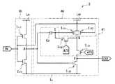
図1は、本発明の第1の実施の形態に係るバッファ回路1(駆動回路)の全体構成の一例を表したものである。バッファ回路1は、入力端INに入力されたパルス信号の位相とほぼ同一位相のパルス信号を出力端OUTから出力するものである。バッファ回路1は、インバータ回路10(入力側インバータ回路)およびインバータ回路20(出力側インバータ回路)を備えている。<First Embodiment>
[Constitution]
FIG. 1 shows an example of the entire configuration of the buffer circuit 1 (drive circuit) according to the first embodiment of the present invention. The
インバータ回路10,20は、入力されたパルス信号の信号波形をほぼ反転させたパルス信号を出力するものである。インバータ回路10,20は、互いに直列に接続されている。インバータ回路10は、インバータ回路20との関係で入力端IN側に配置されており、インバータ回路10の入力端がバッファ回路1の入力端INに相当している。一方、インバータ回路20は、インバータ回路10との関係で出力端OUT側に配置されており、インバータ回路20の出力端がバッファ回路1の出力端OUTに相当している。インバータ回路10の出力端(図中のAに対応する箇所)は、インバータ回路20の入力端に接続されており、バッファ回路1は、インバータ回路10の出力がインバータ回路20に入力されるように構成されている。 The
インバータ回路10は、高電圧線LH1および低電圧線LLの間に挿入されており、インバータ回路20は、高電圧線LH2および低電圧線LLの間に挿入されている。ここで、高電圧線LH1および高電圧線LH2は、互いに分離独立しており、高電圧線LH1および高電圧線LH2に対して互いに異なる電圧を印加することが可能となっている。The
インバータ回路10は、第1導電型のトランジスタTr11と、第2導電型のトランジスタTr12とを有している。トランジスタTr11は、例えば、pチャネル型のMOS(金属酸化膜半導体: Metal Oxide Semiconductor)トランジスタであり、トランジスタTr12は、例えば、nチャネル型のMOSトランジスタである。The
トランジスタTr11およびトランジスタTr12は、互いに並列接続されている。具体的には、トランジスタTr11およびトランジスタTr12のそれぞれのゲートが互いに接続されている。さらに、トランジスタTr11のソースまたはドレインと、トランジスタTr12のソースまたはドレインとが互いに接続されている。また、トランジスタTr11およびトランジスタTr12のそれぞれのゲートは、インバータ回路10の入力端(バッファ回路1の入力端IN)に接続されている。トランジスタTr11のソースまたはドレインと、トランジスタTr12のソースまたはドレインとの接続点Aは、インバータ回路10の出力端に接続されている。トランジスタTr11のソースおよびドレインのうちトランジスタTr12に未接続の方は高電圧線LH1に接続されている。一方、トランジスタTr12のソースおよびドレインのうちトランジスタTr11に未接続の方は低電圧線LLに接続されている。なお、インバータ回路10において、何らかの素子が、トランジスタTr11とトランジスタTr12との間や、トランジスタTr11と高電圧線LH1との間、トランジスタTr12と低電圧線LLとの間に設けられていてもよい。Transistor Tr11 and the transistor Tr12 is connected in parallel to each other. Specifically, the gates of the transistors Tr11 and Tr12 are connected to each other. Further, the source or drain of the transistor Tr11 and the source or drain of the transistor Tr12 are connected to each other. The gates of the transistors Tr11 and Tr12 are connected to the input terminal of the inverter circuit 10 (the input terminal IN of the buffer circuit 1). A connection point A between the source or drain of the transistor Tr11 and the source or drain of the transistor Tr12 is connected to the output terminal of the
インバータ回路20は、第1導電型のトランジスタTr21と、第2導電型のトランジスタTr22と、第1導電型のトランジスタTr23とを有している。トランジスタTr21,Tr23は、例えば、pチャネル型のMOSトランジスタであり、トランジスタTr22は、例えば、nチャネル型のMOSトランジスタである。The
トランジスタTr21,Tr22によって、CMOSトランジスタが構成されている。トランジスタTr21,Tr22において、ドレイン同士が互いに接続されると共にソース同士が互いに接続されている。さらに、トランジスタTr21,Tr22において、ドレインが高電圧線LH2側に接続されると共にソースがインバータ回路20の出力端(バッファ回路1の出力端OUT)に接続されている。トランジスタTr21,Tr22のドレインは、具体的には、後述の閾値補正回路21のトランジスタTr26を介して高電圧線LH2に接続されている。一方、トランジスタTr21,Tr22のソースは、具体的には、トランジスタTr23を介して低電圧線LLに接続されている。The transistors Tr21 and Tr22 constitute a CMOS transistor. In the transistors Tr21 and Tr22 , the drains are connected to each other and the sources are connected to each other. Further, in the transistors Tr21 and Tr22 , the drain is connected to the high voltage line LH2 side, and the source is connected to the output terminal of the inverter circuit 20 (the output terminal OUT of the buffer circuit 1). Specifically, the drains of the transistors Tr21 and Tr22 are connected to the high voltage line LH2 via a transistor Tr26 of the
トランジスタTr21およびトランジスタTr23は、上述のトランジスタTr11およびトランジスタTr12と同様、互いに並列接続されている。トランジスタTr21およびトランジスタTr23のそれぞれのゲートが互いに接続されている。さらに、トランジスタTr21のソースまたはドレインと、トランジスタTr23のソースまたはドレインとが互いに接続されている。トランジスタTr21およびトランジスタTr23のそれぞれのゲートは、インバータ回路10の出力端(接続点A)に接続されている。トランジスタTr21のソースまたはドレインと、トランジスタTr23のソースまたはドレインとの接続点Cは、インバータ回路20の出力端(バッファ回路1の出力端OUT)に接続されている。トランジスタTr23のソースおよびドレインのうちトランジスタTr21に未接続の方は低電圧線LLに接続されている。なお、インバータ回路20において、何らかの素子が、トランジスタTr21とトランジスタTr23との間や、トランジスタTr21と高電圧線LH2との間、トランジスタTr23と低電圧線LLとの間に設けられていてもよい。The transistor Tr21 and the transistor Tr23 are connected in parallel to each other, like the transistor Tr11 and the transistor Tr12 described above. The gates of the transistors Tr21 and Tr23 are connected to each other. Further, the source or drain of the transistor Tr21 and the source or drain of the transistor Tr23 are connected to each other. The gates of the transistors Tr21 and Tr23 are connected to the output terminal (connection point A) of the
インバータ回路20は、さらに、トランジスタTr22のゲート電圧Vg(図示せず)の補正を行う閾値補正回路21(補正回路)を有している。具体的には、閾値補正回路21は、トランジスタTr22のゲートに対して、トランジスタTr22の閾値電圧Vth1(図示せず)またはトランジスタTr22の閾値電圧Vth1に対応する電圧をオフセットとして設定するようになっている。The
閾値補正回路21は、第1導電型のトランジスタTr24(第1トランジスタ)と、第2導電型のトランジスタTr25(第2トランジスタ)と、第1導電型のトランジスタTr26(第3トランジスタ)と、容量素子C21(第1容量素子)とを有している。トランジスタTr24,Tr26は、例えば、pチャネル型のMOSトランジスタであり、トランジスタTr25は、例えば、nチャネル型のMOSトランジスタである。The
トランジスタTr24のソースまたはドレインが、トランジスタTr25のソースまたはドレインと、容量素子C21に接続されている。トランジスタTr24のソースまたはドレインと、トランジスタTr25のソースまたはドレインと、容量素子C21とが互いに接続されている接続点Bは、トランジスタTr22のゲートに接続されている。容量素子C21は、トランジスタTr22のゲート(または接続点B)と、インバータ回路10の入力端との間に挿入されている。トランジスタTr25のソースおよびドレインのうち接続点Bに未接続の方は、トランジスタTr26のソースまたはドレインに接続されている。トランジスタTr26のソースおよびドレインのうちトランジスタTr25のソースまたはドレインと未接続の方は、高電圧線LH2に接続されている。トランジスタTr25のソースまたはドレインと、トランジスタTr26のソースまたはドレインとの接続点Dは、トランジスタTr21,Tr22のドレインに接続されている。なお、閾値補正回路21において、何らかの素子が、トランジスタTr24とトランジスタTr25との間や、トランジスタTr25とトランジスタTr26との間、トランジスタTr24と容量素子C21との間、トランジスタTr24と高電圧線LH2との間、トランジスタTr26と高電圧線LH2との間に設けられていてもよい。The source or drain of the transistor Tr24 is connected to the source or drain of the transistor Tr25 and the capacitor C21 . A connection point B at which the source or drain of the transistor Tr24, the source or drain of the transistor Tr25 , and the capacitor C21 are connected to each other is connected to the gate of the transistor Tr22 . The capacitive element C21 is inserted between the gate (or connection point B) of the transistor Tr22 and the input terminal of the
閾値補正回路21内の3つのトランジスタ(トランジスタTr24〜Tr26)のゲートは、それぞれ、図示しない制御信号線に接続されており、トランジスタTr24〜Tr26のゲートには、その制御信号線を介して制御信号AZ1〜AZ3が入力されるようになっている。The gates of the three transistors (transistors Tr24 to Tr26 ) in the
[動作]
次に、本実施の形態のバッファ回路1の動作について説明する。以下では、主として、バッファ回路1における閾値補正(Vthキャンセル)について説明する。[Operation]
Next, the operation of the
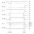
図2は、バッファ回路1の動作の一例を表したものである。図2には、トランジスタTr22のゲート−ソース間電圧Vgsに含まれる閾値電圧Vth1をキャンセルする動作の一例が示されている。なお、高電圧線LH2の電圧は、図2(A)に示したように、この動作の間、常に一定値(Vdd)となっているものとする。FIG. 2 shows an example of the operation of the
当初、バッファ回路1の入力端INにはVssが入力されており、接続点A(インバータ回路10の出力端)の電圧がVddとなっている。そのため、トランジスタTr21がオフしており、トランジスタTr22がオンしている。このとき、制御信号AZ1はVddとなっており、制御信号AZ2,AZ3はともにVssとなっている。そのため、トランジスタTr24,Tr25がオフし、トランジスタTr26がオンしている。次に、制御信号AZ1がVssとなると共に、制御信号AZ3がVddとなり(T1)、トランジスタTr24がオンすると共にトランジスタTr26がオフする。すると、接続点Bの電圧がVddとなる。次に、制御信号AZ1がVddとなり(T2)、トランジスタTr24がオフしたのち、制御信号AZ2がVddよりも少し大きな電圧値となり(T3)、トランジスタTr25がオンする。すると、トランジスタTr25,Tr22に電流が流れ、接続点Bの電圧が徐々に下降し、やがてVss+Vth1となったところで、トランジスタTr22がオフする。これにより、接続点Bの電圧の下降がVss+Vth1で停止し、接続点Bの電圧がVss+Vth1に保持される。つまり、上記の一連の動作を行うことにより、トランジスタTr22のゲートに対して、トランジスタTr22の閾値電圧Vth1またはトランジスタTr22の閾値電圧Vth1に対応する電圧をオフセットとして設定する。その結果、トランジスタTr22の閾値電圧Vth1にばらつきがあった場合であっても、バッファ回路1の入力端INへのVddの入力パルスに応じて、バッファ回路1の出力端OUTからVddの出力パルスを、幅のばらつきなく正確に出力することができる。従って、バッファ回路1の出力電圧がVssからVddに立ち上がるタイミングにおいて、ばらつきを低減することができる。Initially, Vss is input to the input terminal IN of the
このように、本実施の形態のバッファ回路1では、トランジスタTr22のゲートに対して、トランジスタTr22の閾値電圧Vth1またはトランジスタTr22の閾値電圧Vth1に対応する電圧がオフセットとして設定される。これにより、バッファ回路1の出力電圧が立ち上がるタイミングにおいて、ばらつきを低減することができる。Thus, in the
ところで、本実施の形態のバッファ回路1を、例えば、有機EL表示装置のスキャナの出力段に適用した場合には、移動度補正期間をバッファ回路1の出力電圧のパルス幅で規定することができる。これにより、移動度補正期間のばらつきを低減することができるので、発光時に有機EL素子に流れる電流のばらつきを低減することができ、輝度の均一性を向上させることができる。 By the way, when the
<第1の実施の形態の変形例>
上記実施の形態では、トランジスタTr24がpチャネル型のMOSトランジスタとなっており、かつトランジスタTr25がnチャネル型のMOSトランジスタとなっていたが、これらのトランジスタTr24,Tr25の導電型が全て、逆になっていてもよい。具体的には、図3に示したように、トランジスタTr24がnチャネル型のMOSトランジスタとなっており、かつトランジスタTr25がpチャネル型のMOSトランジスタとなっていてもよい。ただし、その場合には、例えば、図4に示したように、制御信号AZ1,AZ2の信号波形を、図2に示した制御信号AZ1,AZ2の信号波形を反転させた波形とすることが必要である。<Modification of the first embodiment>
In the above embodiment, the transistor Tr24 is a p-channel MOS transistor and the transistor Tr25 is an n-channel MOS transistor. However, the conductivity type of these transistors Tr24 and Tr25 is All may be reversed. Specifically, as shown in FIG. 3, the transistor Tr24 may be an n-channel MOS transistor, and the transistor Tr25 may be a p-channel MOS transistor. However, in this case, for example, as shown in FIG. 4, the signal waveforms of the control signals AZ1 and AZ2 need to be inverted from the signal waveforms of the control signals AZ1 and AZ2 shown in FIG. It is.
<第2の実施の形態>
次に、本発明の第2の実施の形態に係るバッファ回路2(駆動回路)について説明する。図5は、バッファ回路2の全体構成の一例を表したものである。バッファ回路2は、上記のバッファ回路1と同様、入力端INに入力されたパルス信号の位相とほぼ同一位相のパルス信号を出力端OUTから出力するものである。バッファ回路2は、インバータ回路10(入力側インバータ回路)およびインバータ回路30(出力側インバータ回路)を備えている。<Second Embodiment>
Next, a buffer circuit 2 (drive circuit) according to a second embodiment of the present invention will be described. FIG. 5 illustrates an example of the overall configuration of the
インバータ回路30は、入力されたパルス信号の信号波形をほぼ反転させたパルス信号を出力するものである。インバータ回路10,30は、互いに直列に接続されている。インバータ回路10は、インバータ回路30との関係で入力端IN側に配置されており、インバータ回路10の入力端がバッファ回路2の入力端INに相当している。一方、インバータ回路30は、インバータ回路10との関係で出力端OUT側に配置されており、インバータ回路30の出力端がバッファ回路2の出力端OUTに相当している。インバータ回路10の出力端(図中のAに対応する箇所)は、インバータ回路30の入力端に接続されており、バッファ回路2は、インバータ回路10の出力がインバータ回路30に入力されるように構成されている。インバータ回路30は、高電圧線LH2および低電圧線LLの間に挿入されている。The
インバータ回路30は、上記実施の形態のインバータ回路20において、閾値補正回路21の代わりに、閾値補正回路31を設けた回路構成となっている。閾値補正回路31は、トランジスタTr21のゲート電圧Vg(図示せず)の補正を行うものである。具体的には、閾値補正回路31は、トランジスタTr21のゲートに対して、トランジスタTr21の閾値電圧Vth2(図示せず)またはトランジスタTr21の閾値電圧Vth2に対応する電圧をオフセットとして設定するようになっている。The
閾値補正回路31は、第2導電型のトランジスタTr31(第4トランジスタ)と、第2導電型のトランジスタTr32(第5トランジスタ)と、第1導電型のトランジスタTr33(第6トランジスタ)と、容量素子C31(第2容量素子)とを有している。トランジスタTr31,Tr32は、例えば、nチャネル型のMOSトランジスタであり、トランジスタTr33は、例えば、pチャネル型のMOSトランジスタである。The
トランジスタTr31のソースまたはドレインが、トランジスタTr32のソースまたはドレインと、容量素子C31に接続されている。トランジスタTr31のソースまたはドレインと、トランジスタTr32のソースまたはドレインと、容量素子C31とが互いに接続されている接続点Eは、トランジスタTr21のゲートに接続されている。容量素子C31は、トランジスタTr21のゲート(または接続点E)と、インバータ回路10の入力端との間に挿入されている。トランジスタTr32のソースおよびドレインのうち接続点Eに未接続の方は、トランジスタTr33のソースまたはドレインに接続されている。トランジスタTr33のソースおよびドレインのうちトランジスタTr32のソースまたはドレインと未接続の方は、トランジスタTr23のソースおよびドレインのうち低電圧線LLと未接続の方と接続されている。トランジスタTr33のソースまたはドレインと、トランジスタTr23のソースまたはドレインとの接続点Fは、インバータ回路30の出力端(バッファ回路2の出力端OUT)に接続されている。トランジスタTr32のソースまたはドレインと、トランジスタTr33のソースまたはドレインとの接続点Gは、トランジスタTr21,Tr22のソースに接続されている。なお、閾値補正回路31において、何らかの素子が、トランジスタTr31とトランジスタTr32との間や、トランジスタTr32とトランジスタTr33との間、トランジスタTr32と容量素子C31との間、トランジスタTr31と低電圧線LLとの間、トランジスタTr33と低電圧線LLとの間に設けられていてもよい。The source or drain of the transistor Tr31 is a source or drain of the transistor Tr32, and is connected to the capacitor C31. A connection point E where the source or drain of the transistor Tr31, the source or drain of the transistor Tr32 , and the capacitor C31 are connected to each other is connected to the gate of the transistor Tr21 . The capacitive element C31 is inserted between the gate (or connection point E) of the transistor Tr21 and the input terminal of the
閾値補正回路31内の3つのトランジスタ(トランジスタTr31〜Tr33)のゲートは、それぞれ、図示しない制御信号線に接続されており、トランジスタTr31〜Tr33のゲートには、その制御信号線を介して制御信号AZ4〜AZ6が入力されるようになっている。The gates of the three transistors (transistors Tr31 to Tr33 ) in the
[動作]
次に、本実施の形態のバッファ回路2の動作について説明する。以下では、主として、バッファ回路2における閾値補正(Vthキャンセル)について説明する。[Operation]
Next, the operation of the
図6は、バッファ回路2の動作の一例を表したものである。図6には、トランジスタTr21のゲート−ソース間電圧Vgsに含まれる閾値電圧Vth2をキャンセルする動作の一例が示されている。なお、高電圧線LH2の電圧は、図6(A)に示したように、この動作の間、常に一定値(Vdd)となっているものとする。FIG. 6 illustrates an example of the operation of the
当初、バッファ回路2の入力端INにはVssが入力されており、接続点A(インバータ回路10の出力端)の電圧がVddとなっている。そのため、トランジスタTr21がオフしており、トランジスタTr22がオンしている。このとき、制御信号AZ4〜AZ6はともにVssとなっており、トランジスタTr31,Tr32がオフし、トランジスタTr33がオンしている。次に、制御信号AZ4がVddとなると共に、制御信号AZ6がVddとなり(T1)、トランジスタTr31がオンすると共にトランジスタTr33がオフする。すると、接続点Eの電圧がVssとなる。次に、制御信号AZ4がVssとなり(T2)、トランジスタTr31がオフしたのち、制御信号AZ5がVddよりも少し大きな電圧値となり(T3)、トランジスタTr32がオンする。すると、トランジスタTr32,Tr22に電流が流れ、接続点Eの電圧が徐々に上昇し、やがてVdd+Vth2となったところで、トランジスタTr22がオフする。これにより、接続点Eの電圧の上昇がVdd+Vth2で停止し、接続点Eの電圧がVdd+Vth2に保持される。つまり、上記の一連の動作を行うことにより、トランジスタTr21のゲートに対して、トランジスタTr21の閾値電圧Vth2またはトランジスタTr21の閾値電圧Vth2に対応する電圧をオフセットとして設定する。その結果、トランジスタTr21の閾値電圧Vth2にばらつきがあった場合であっても、バッファ回路2の入力端INへのVddの入力パルスに応じて、バッファ回路2の出力端OUTからVddの出力パルスを、幅のばらつきなく正確に出力することができる。従って、バッファ回路2の出力電圧がVssからVddに立ち上がるタイミングにおいて、ばらつきを低減することができる。Initially, Vss is input to the input terminal IN of the
このように、本実施の形態のバッファ回路2では、トランジスタTr21のゲートに対して、トランジスタTr21の閾値電圧Vth2またはトランジスタTr21の閾値電圧Vth2に対応する電圧がオフセットとして設定される。これにより、バッファ回路2の出力電圧が立ち上がるタイミングにおいて、ばらつきを低減することができる。Thus, the
ところで、本実施の形態のバッファ回路2を、例えば、有機EL表示装置のスキャナの出力段に適用した場合には、移動度補正期間をバッファ回路2の出力電圧のパルス幅で規定することができる。これにより、移動度補正期間のばらつきを低減することができるので、発光時に有機EL素子に流れる電流のばらつきを低減することができ、輝度の均一性を向上させることができる。 By the way, when the
<第2の実施の形態の変形例>
上記第2の実施の形態では、トランジスタTr31,Tr32がnチャネル型のMOSトランジスタとなっていたが、これらのトランジスタTr31,Tr32の導電型が全て、逆になっていてもよい。具体的には、図7に示したように、トランジスタTr31,Tr32がpチャネル型のMOSトランジスタとなっていてもよい。ただし、その場合には、例えば、図8に示したように、制御信号AZ4,AZ5の信号波形を、図6に示した制御信号AZ4,AZ5の信号波形を反転させた波形とすることが必要である。<Modification of Second Embodiment>
In the second embodiment, the transistors Tr31 and Tr32 are n-channel MOS transistors. However, the conductivity types of these transistors Tr31 and Tr32 may all be reversed. Specifically, as shown in FIG. 7, the transistors Tr31 and Tr32 may be p-channel MOS transistors. However, in this case, for example, as shown in FIG. 8, the signal waveforms of the control signals AZ4 and AZ5 need to be inverted from the signal waveforms of the control signals AZ4 and AZ5 shown in FIG. It is.
<第3の実施の形態>
次に、本発明の第3の実施の形態に係るバッファ回路3(駆動回路)について説明する。図9は、バッファ回路3の全体構成の一例を表したものである。バッファ回路3は、上記のバッファ回路2と同様、入力端INに入力されたパルス信号の位相とほぼ同一位相のパルス信号を出力端OUTから出力するものである。バッファ回路3は、インバータ回路10(入力側インバータ回路)およびインバータ回路40(出力側インバータ回路)を備えている。<Third Embodiment>
Next, a buffer circuit 3 (drive circuit) according to a third embodiment of the present invention will be described. FIG. 9 illustrates an example of the entire configuration of the
インバータ回路40は、入力されたパルス信号の信号波形をほぼ反転させたパルス信号を出力するものである。インバータ回路10,40は、互いに直列に接続されている。インバータ回路10は、インバータ回路40との関係で入力端IN側に配置されており、インバータ回路10の入力端がバッファ回路3の入力端INに相当している。一方、インバータ回路40は、インバータ回路10との関係で出力端OUT側に配置されており、インバータ回路40の出力端がバッファ回路3の出力端OUTに相当している。インバータ回路10の出力端(図中のAに対応する箇所)は、インバータ回路40の入力端に接続されており、バッファ回路3は、インバータ回路10の出力がインバータ回路40に入力されるように構成されている。インバータ回路40は、高電圧線LH2および低電圧線LLの間に挿入されている。The
インバータ回路40は、上記第2の実施の形態のインバータ回路30において、閾値補正回路31の代わりに、閾値補正回路41を設けた回路構成となっている。ここで、閾値補正回路41は、上記第2の実施の形態の閾値補正回路31において、トランジスタTr31をなくした回路構成となっている。また、閾値補正回路41において、トランジスタTr32が、第2導電型のMOSトランジスタ、例えば、pチャネル型のMOSトランジスタとなっている。The
[動作]
次に、本実施の形態のバッファ回路3の動作について説明する。以下では、主として、バッファ回路3における閾値補正(Vthキャンセル)について説明する。[Operation]
Next, the operation of the
図10は、バッファ回路3の動作の一例を表したものである。図10には、トランジスタTr21のゲート−ソース間電圧Vgsに含まれる閾値電圧Vth2をキャンセルする動作の一例が示されている。なお、本実施の形態では、高電圧線LH2には、図10(A)に示したように、所定のタイミングでVddからVssに立ち下がるパルス信号が印加される点が、上記第1の実施の形態と大きく異なっている。FIG. 10 shows an example of the operation of the
バッファ回路3の入力端INにVssが入力される(T1)。すると、接続点A(インバータ回路10の出力端)の電圧がVddとなる。そのため、トランジスタTr21がオフすると共に、トランジスタTr22がオンする。このとき、制御信号AZ5はVddとなっており、さらに制御信号AZ6はVssとなっている。これにより、トランジスタTr32がオフし、トランジスタTr33がオンしている。次に、制御信号AZ5はVssとなり(T2)、トランジスタTr32がオンする。すると、接続点Eの電圧がVssとなる。次に、制御信号AZ6がVddとなり(T3)、トランジスタTr33がオフしたのち、高電圧線LH2の電圧がVssからVddに立ち上る(T4)。すると、トランジスタTr32,Tr22に電流が流れ、接続点Eの電圧が徐々に上昇し、やがてVdd+Vth2となったところで、トランジスタTr22がオフする。これにより、接続点Eの電圧の上昇がVdd+Vth2で停止し、接続点Eの電圧がVdd+Vth2に保持される。つまり、上記の一連の動作を行うことにより、トランジスタTr21のゲートに対して、トランジスタTr21の閾値電圧Vth2またはトランジスタTr21の閾値電圧Vth2に対応する電圧をオフセットとして設定する。その結果、トランジスタTr21の閾値電圧Vth2にばらつきがあった場合であっても、バッファ回路3の入力端INへのVddの入力パルスに応じて、バッファ回路3の出力端OUTからVddの出力パルスを、幅のばらつきなく正確に出力することができる。従って、バッファ回路3の出力電圧がVssからVddに立ち上がるタイミングにおいて、ばらつきを低減することができる。Vss is input to the input terminal IN of the buffer circuit 3 (T1 ). Then, the voltage at the connection point A (the output terminal of the inverter circuit 10) becomesVdd . Therefore, the transistor Tr21 is turned off and the transistor Tr22 is turned on. At this time, the control signal AZ5 is Vdd and the control signal AZ6 is Vss . Thus, the transistor Tr32 is turned off, the transistor Tr33 is turned on. Next, the control signal AZ5 becomes Vss (T2 ), and the transistor Tr32 is turned on. Then, the voltage at the connection point E becomes Vss . Next, the control signal AZ6 becomes Vdd (T3 ), and after the transistor Tr33 is turned off, the voltage of the high voltage line LH2 rises from Vss to Vdd (T4 ). Then, current flows through the transistors Tr32 and Tr22, and the voltage at the connection point E gradually rises. When the voltage reaches Vdd + Vth2 , the transistor Tr22 is turned off. As a result, the increase in the voltage at the connection point E stops at Vdd + Vth2 , and the voltage at the connection point E is held at Vdd + Vth2 . In other words, by performing the series of operations described above, it sets the gate of the transistor Tr21, a voltage corresponding to the threshold voltage Vth2 of the threshold voltage Vth2 or transistor Tr21 of the transistor Tr21 as an offset. As a result, even when there are variations in the threshold voltage Vth2 of the transistors Tr21, in response to an input pulse of Vdd to input terminal IN of the
このように、本実施の形態のバッファ回路3では、トランジスタTr21のゲートに対して、トランジスタTr21の閾値電圧Vth2またはトランジスタTr21の閾値電圧Vth2に対応する電圧がオフセットとして設定される。これにより、バッファ回路3の出力電圧が立ち上がるタイミングにおいて、ばらつきを低減することができる。Thus, in the
ところで、本実施の形態のバッファ回路3を、例えば、有機EL表示装置のスキャナの出力段に適用した場合には、移動度補正期間をバッファ回路3の出力電圧のパルス幅で規定することができる。これにより、移動度補正期間のばらつきを低減することができるので、発光時に有機EL素子に流れる電流のばらつきを低減することができ、輝度の均一性を向上させることができる。 By the way, when the
<第3の実施の形態の変形例>
上記第3の実施の形態では、トランジスタTr32がpチャネル型のMOSトランジスタとなっていたが、このトランジスタTr32の導電型が、逆になっていてもよい。具体的には、図11に示したように、トランジスタTr32がnチャネル型のMOSトランジスタとなっていてもよい。ただし、その場合には、例えば、図12に示したように、制御信号AZ5の信号波形を、図10に示した制御信号AZ5の信号波形を反転させた波形とすることが必要である。<Modification of Third Embodiment>
In the third embodiment, the transistor Tr32 is a p-channel MOS transistor. However, the conductivity type of the transistor Tr32 may be reversed. Specifically, as shown in FIG. 11, the transistor Tr32 may be an n-channel MOS transistor. However, in that case, for example, as shown in FIG. 12, the signal waveform of the control signal AZ5 needs to be a waveform obtained by inverting the signal waveform of the control signal AZ5 shown in FIG.
<第4の実施の形態>
次に、本発明の第4の実施の形態に係るバッファ回路4(駆動回路)について説明する。図13は、バッファ回路4の全体構成の一例を表したものである。バッファ回路4は、上記のバッファ回路1,2と同様、入力端INに入力されたパルス信号の位相とほぼ同一位相のパルス信号を出力端OUTから出力するものである。バッファ回路4は、インバータ回路10(入力側インバータ回路)およびインバータ回路50(出力側インバータ回路)を備えている。<Fourth embodiment>
Next, a buffer circuit 4 (drive circuit) according to a fourth embodiment of the present invention will be described. FIG. 13 illustrates an example of the entire configuration of the
インバータ回路50は、入力されたパルス信号の信号波形をほぼ反転させたパルス信号を出力するものである。インバータ回路10,50は、互いに直列に接続されている。インバータ回路10は、インバータ回路50との関係で入力端IN側に配置されており、インバータ回路10の入力端がバッファ回路4の入力端INに相当している。一方、インバータ回路50は、インバータ回路10との関係で出力端OUT側に配置されており、インバータ回路50の出力端がバッファ回路4の出力端OUTに相当している。インバータ回路10の出力端(図中のAに対応する箇所)は、インバータ回路50の入力端に接続されており、バッファ回路4は、インバータ回路10の出力がインバータ回路50に入力されるように構成されている。インバータ回路50は、高電圧線LH2および低電圧線LLの間に挿入されている。The
インバータ回路50は、上記第2の実施の形態のインバータ回路30において、閾値補正回路31の代わりに、閾値補正回路41を設けた回路構成となっている。ここで、閾値補正回路41は、上記第1の実施の形態の閾値補正回路21と、上記第2の実施の形態の閾値補正回路31とを組み合わせたものである。なお、閾値補正回路21,31を組み合わせるにあたって、トランジスタTr21,Tr22のそれぞれのドレインが互いに分離されると共に、トランジスタTr21,Tr22のそれぞれのソースも互いに分離されている。さらに、トランジスタTr21のドレインが直接、高電圧線LH2に接続されており、トランジスタTr22のドレインが、トランジスタTr26のソースまたはドレインと、トランジスタTr25のソースまたはドレインとの接続点Hに接続されている。また、トランジスタTr22のソースが直接、バッファ回路4の出力端OUTに接続されており、トランジスタTr21のソースが、トランジスタTr32のソースまたはドレインと、トランジスタTr33のソースまたはドレインとの接続点Iに接続されている。The
さらに、制御信号AZ3が制御信号AZ6と共用されている。また、制御信号AZ1と、制御信号AZ4とが互いに同じ信号となっており、制御信号AZ2と、制御信号AZ5とが互いに同じ信号となっている。なお、トランジスタTr24は、第2導電型のトランジスタ、例えば、nチャネル型のMOSトランジスタである。Further, the control signal AZ3 is shared with the control signal AZ6. Further, the control signal AZ1 and the control signal AZ4 are the same signal, and the control signal AZ2 and the control signal AZ5 are the same signal. The transistor Tr24 is a second conductivity type transistor, for example, an n-channel type MOS transistor.
[動作]
次に、本実施の形態のバッファ回路4の動作について説明する。以下では、主として、バッファ回路4における閾値補正(Vthキャンセル)について説明する。[Operation]
Next, the operation of the
図14は、バッファ回路4の動作の一例を表したものである。図14には、トランジスタTr21,Tr22のそれぞれのゲート−ソース間電圧Vgsに含まれる閾値電圧Vth1,Vth2をキャンセルする動作の一例が示されている。なお、高電圧線LH2の電圧は、図14(A)に示したように、この動作の間、常に一定値(Vdd)となっているものとする。FIG. 14 shows an example of the operation of the
当初、バッファ回路4の入力端INにはVssが入力されており、接続点A(インバータ回路10の出力端)の電圧がVdd+Vth2となっており、接続点Bの電圧がVssとなっている。そのため、トランジスタTr21,Tr22がともにオフしている。このとき、制御信号AZ1,AZ4は共にVssとなっており、制御信号AZ2,AZ5も共にVssとなっており、制御信号AZ3もVssとなっている。そのため、トランジスタTr24,Tr25,Tr31,Tr32がオフし、トランジスタTr26,Tr33がオンしている。次に、制御信号AZ1,AZ4がVddとなると共に、制御信号AX3がVddとなり(T1)、トランジスタTr24,Tr31がオンすると共にトランジスタTr26,Tr33がオフする。すると、接続点Aの電圧がVssとなり、接続点Bの電圧がVddとなる。次に、制御信号AZ1,AZ4がVssとなり(T2)、トランジスタTr24,Tr31がオフしたのち、制御信号AZ2,AZ5がVddよりも少し大きな電圧値となり(T3)、トランジスタTr25,Tr32がオンする。すると、トランジスタTr32,Tr21に電流が流れ、接続点Aの電圧が徐々に上昇し、やがてVdd+Vth2となったところで、トランジスタTr21がオフする。これにより、接続点Aの電圧の上昇がVdd+Vth2で停止し、接続点Aの電圧がVdd+Vth2に保持される。一方、トランジスタTr25,Tr22にも電流が流れ、接続点Bの電圧が徐々に下降し、やがてVss+Vth1となったところで、トランジスタTr22がオフする。これにより、接続点Bの電圧の下降がVss+Vth1で停止し、接続点Bの電圧がVss+Vth1に保持される。つまり、上記の一連の動作を行うことにより、トランジスタTr21のゲートに対して、トランジスタTr21の閾値電圧Vth2またはトランジスタTr21の閾値電圧Vth2に対応する電圧をオフセットとして設定すると共に、トランジスタTr22のゲートに対して、トランジスタTr22の閾値電圧Vth1またはトランジスタTr22の閾値電圧Vth1に対応する電圧をオフセットとして設定する。その結果、トランジスタTr21の閾値電圧Vth2にばらつきがあった場合であっても、バッファ回路4の入力端INへのVddの入力パルスに応じて、バッファ回路4の出力端OUTからVddの出力パルスを、幅のばらつきなく正確に出力することができる。さらに、トランジスタTr22の閾値電圧Vth1にばらつきがあった場合であっても、バッファ回路4の入力端INへのVddの入力パルスに応じて、バッファ回路4の出力端OUTからVddの出力パルスを、幅のばらつきなく正確に出力することができる。従って、バッファ回路4の出力電圧がVssからVddに立ち上がるタイミングにおいて、ばらつきを低減することができる。Initially, Vss is input to the input terminal IN of the
このように、本実施の形態のバッファ回路4では、トランジスタTr21のゲートに対して、トランジスタTr21の閾値電圧Vth2またはトランジスタTr21の閾値電圧Vth2に対応する電圧がオフセットとして設定される。さらに、トランジスタTr22のゲートに対して、トランジスタTr22の閾値電圧Vth1またはトランジスタTr22の閾値電圧Vth1に対応する電圧がオフセットとして設定される。これにより、バッファ回路4の出力電圧が立ち上がるタイミングにおいて、ばらつきを低減することができる。Thus, in the
ところで、本実施の形態のバッファ回路4を、例えば、有機EL表示装置のスキャナの出力段に適用した場合には、移動度補正期間をバッファ回路4の出力電圧のパルス幅で規定することができる。これにより、移動度補正期間のばらつきを低減することができるので、発光時に有機EL素子に流れる電流のばらつきを低減することができ、輝度の均一性を向上させることができる。 By the way, when the
<第4の実施の形態の変形例>
上記実施の形態では、トランジスタTr24,Tr25,Tr31,Tr32がnチャネル型のMOSトランジスタとなっていたが、これらのトランジスタTr24,Tr25,Tr31,Tr32の導電型が全て、逆になっていてもよい。具体的には、図15に示したように、トランジスタTr24,Tr25,Tr31,Tr32がpチャネル型のMOSトランジスタとなっていてもよい。ただし、その場合には、例えば、図16に示したように、制御信号AZ1,AZ2,AZ4,AZ5の信号波形を、図14に示した制御信号AZ1,AZ2,AZ4,AZ5の信号波形を反転させた波形とすることが必要である。<Modification of Fourth Embodiment>
In the above embodiment, the transistors Tr24 , Tr25 , Tr31 , Tr32 are n-channel MOS transistors. However, the conductivity types of these transistors Tr24 , Tr25 , Tr31 , Tr32 are all , May be reversed. Specifically, as shown in FIG. 15, the transistors Tr24 , Tr25 , Tr31 , Tr32 may be p-channel MOS transistors. However, in that case, for example, as shown in FIG. 16, the signal waveforms of the control signals AZ1, AZ2, AZ4, and AZ5 are inverted, and the signal waveforms of the control signals AZ1, AZ2, AZ4, and AZ5 shown in FIG. It is necessary to have a waveform that has been made to be.
<適用例>
図17は、上記各実施の形態に係るバッファ回路1〜4の適用例の一例である表示装置100の全体構成の一例を表したものである。この表示装置100は、例えば、表示パネル110(表示部)と、駆動回路120(駆動部)とを備えている。<Application example>
FIG. 17 illustrates an example of the entire configuration of the display device 100 which is an example of an application example of the
(表示パネル110)
表示パネル110は、発光色の互いに異なる3種類の有機EL素子111R,111G,111Bが2次元配置された表示領域110Aを有している。表示領域110Aとは、有機EL素子111R,111G,111Bから発せられる光を利用して映像を表示する領域である。有機EL素子111Rは赤色光を発する有機EL素子であり、有機EL素子111Gは緑色光を発する有機EL素子であり、有機EL素子111Bは青色光を発する有機EL素子である。なお、以下では、有機EL素子111R,111G,111Bの総称として有機EL素子111を適宜、用いるものとする。(Display panel 110)
The
(表示領域110A)
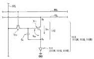
図18は、表示領域10A内の回路構成の一例を、後述の書込線駆動回路124の一例と共に表したものである。表示領域110A内には、複数の画素回路112が個々の有機EL素子111と対となって2次元配置されている。なお、本適用例では、一対の有機EL素子111および画素回路112が1つの画素113を構成している。より詳細には、図18に示したように、一対の有機EL素子111Rおよび画素回路112が1つの赤色用の画素113Rを構成し、一対の有機EL素子111Gおよび画素回路112が1つの緑色用の画素113Gを構成し、一対の有機EL素子111Bおよび画素回路112が1つの青色用の画素113Bを構成している。さらに、互いに隣り合う3つの画素113R,113G,113Bが1つの表示画素114を構成している。(
FIG. 18 illustrates an example of a circuit configuration in the
各画素回路112は、例えば、有機EL素子111に流れる電流を制御する駆動トランジスタTr1と、信号線DTLの電圧を駆動トランジスタTr1に書き込む書き込みトランジスタTr2と、保持容量Csとによって構成されたものであり、2Tr1Cの回路構成となっている。駆動トランジスタTr1および書き込みトランジスタTr2は、例えば、nチャネルMOS型の薄膜トランジスタ(TFT(Thin Film Transistor))により形成されている。駆動トランジスタTr1または書き込みトランジスタTr2は、例えば、pチャネルMOS型のTFTであってもよい。Each
表示領域110Aにおいて、複数の書込線WSL(走査線)が行状に配置され、複数の信号線DTLが列状に配置されている。表示領域110Aには、さらに、複数の電源線PSL(電源電圧の供給される部材)が書込線WSLに沿って行状に配置されている。各信号線DTLと各書込線WSLとの交差点近傍には、有機EL素子111が1つずつ設けられている。各信号線DTLは、後述の信号線駆動回路123の出力端(図示せず)と、書き込みトランジスタTr2のドレイン電極およびソース電極のいずれか一方(図示せず)に接続されている。各書込線WSLは、後述の書込線駆動回路124の出力端(図示せず)と、書き込みトランジスタTr2のゲート電極(図示せず)に接続されている。各電源線PSLは、後述の電源線駆動回路125の出力端(図示せず)と、駆動トランジスタTr1のドレイン電極およびソース電極のいずれか一方(図示せず)に接続されている。書き込みトランジスタTr2のドレイン電極およびソース電極のうち信号線DTLに非接続の方(図示せず)は、駆動トランジスタTr1のゲート電極(図示せず)と、保持容量Csの一端に接続されている。駆動トランジスタTr1のドレイン電極およびソース電極のうち電源線PSLに非接続の方(図示せず)と保持容量Csの他端とが、有機EL素子111のアノード電極(図示せず)に接続されている。有機EL素子111のカソード電極(図示せず)は、例えば、グラウンド線GNDに接続されている。In the
(駆動回路120)
次に、駆動回路120内の各回路について、図17、図18を参照して説明する。駆動回路120は、タイミング生成回路121、映像信号処理回路122、信号線駆動回路123、書込線駆動回路124、および電源線駆動回路125を有している。(Drive circuit 120)
Next, each circuit in the
タイミング生成回路121は、映像信号処理回路122、信号線駆動回路123、書込線駆動回路124、および電源線駆動回路125が連動して動作するように制御するものである。タイミング生成回路121は、例えば、外部から入力された同期信号20Bに応じて(同期して)、上述した各回路に対して制御信号121Aを出力するようになっている。 The
映像信号処理回路122は、外部から入力された映像信号120Aに対して所定の補正を行うと共に、補正した後の映像信号122Aを信号線駆動回路123に出力するようになっている。所定の補正としては、例えば、ガンマ補正や、オーバードライブ補正などが挙げられる。 The video
信号線駆動回路123は、制御信号121Aの入力に応じて(同期して)、映像信号処理回路122から入力された映像信号122A(信号電圧Vsig)を各信号線DTLに印加して、選択対象の画素113に書き込むものである。なお、書き込みとは、駆動トランジスタTr1のゲートに所定の電圧を印加することを指している。In response to (in synchronization with) the input of the
信号線駆動回路123は、例えばシフトレジスタ(図示せず)を含んで構成されており、画素113の各列に対応して、1段ごとにバッファ回路(図示せず)を備えている。この信号線駆動回路123は、制御信号121Aの入力に応じて(同期して)、各信号線DTLに対して、2種類の電圧(Vofs、Vsig)を出力可能となっている。具体的には、信号線駆動回路123は、各画素113に接続された信号線DTLを介して、書込線駆動回路124により選択された画素113へ2種類の電圧(Vofs、Vsig)を順番に供給するようになっている。The signal
ここで、オフセット電圧Vofsは、有機EL素子111の閾値電圧Velよりも低い電圧値となっている。また、信号電圧Vsigは、映像信号122Aに対応する電圧値となっている。信号電圧Vsigの最小電圧はオフセット電圧Vofsよりも低い電圧値となっており、信号電圧Vsigの最大電圧はオフセット電圧Vofsよりも高い電圧値となっている。Here, the offset voltage Vofs has a voltage value lower than the threshold voltage Vel of the
書込線駆動回路124は、例えばシフトレジスタ(図示せず)を含んで構成されており、画素113の各行に対応して、1段ごとにバッファ回路1、バッファ回路2、バッファ回路3、またはバッファ回路4を備えている。この書込線駆動回路124は、制御信号121Aの入力に応じて(同期して)、各書込線WSLに対して、2種類の電圧(Vdd、Vss)を出力可能となっている。具体的には、書込線駆動回路124は、各画素113に接続された書込線WSLを介して、駆動対象の画素113へ2種類の電圧(Vdd、Vss)を供給し、書き込みトランジスタTr2を制御するようになっている。The write
ここで、電圧Vddは、書き込みトランジスタTr2のオン電圧以上の値となっている。Vddは、後述の消光時や閾値補正時に、書込線駆動回路124から出力される電圧値である。Vssは、書き込みトランジスタTr2のオン電圧よりも低い値となっており、かつ、Vddよりも低い値となっている。Here, the voltage Vdd is a value equal to or higher than the ON voltage of the write transistor Tr2 . Vdd is a voltage value output from the write
電源線駆動回路125は、例えばシフトレジスタ(図示せず)を含んで構成されており、例えば、画素113の各行に対応して、1段ごとにバッファ回路(図示せず)を備えている。この電源線駆動回路125は、制御信号121Aの入力に応じて(同期して)、2種類の電圧(VccH、VccL)を出力可能となっている。具体的には、電源線駆動回路125は、各画素113に接続された電源線PSLを介して、駆動対象の画素113へ2種類の電圧(VccH、VccL)を供給し、有機EL素子111の発光および消光を制御するようになっている。The power supply
ここで、電圧VccLは、有機EL素子111の閾値電圧Velと、有機EL素子111のカソードの電圧Vcaとを足し合わせた電圧(Vel+Vca)よりも低い電圧値である。また、電圧VccHは、電圧(Vel+Vca)以上の電圧値である。Here, the voltage VccL is a voltage value lower than a voltage (Vel + Vca ) obtained by adding the threshold voltage Vel of the
次に、本適用例の表示装置100の動作(消光から発光までの動作)の一例について説明する。本適用例では、駆動トランジスタTr1の閾値電圧Vthや移動度μが経時変化したりしても、それらの影響を受けることなく、有機EL素子111の発光輝度を一定に保つようにするために、閾値電圧Vthや移動度μの変動に対する補正動作が組み込まれている。Next, an example of the operation (operation from extinction to light emission) of the display device 100 of this application example will be described. In this application example, even if the threshold voltage Vth and the mobility μ of the driving transistor Tr1 change with time, the light emission luminance of the
図19は、画素回路112に印加される電圧波形の一例と、駆動トランジスタTr1のゲート電圧Vgおよびソース電圧Vsの変化の一例とを表したものである。図19(A)には信号線DTLに、信号電圧Vsigと、オフセット電圧Vofsが印加されている様子が示されている。図19(B)には書込線WSLに、駆動トランジスタTr1をオンする電圧Vddと、駆動トランジスタTr1をオフする電圧Vssが印加されている様子が示されている。図19(C)には電源線PSLに、電圧VccHと、電圧VccLが印加されている様子が示されている。さらに、図19(D),(E)には、電源線PSL、信号線DTLおよび書込線WSLへの電圧印加に応じて、駆動トランジスタTr1のゲート電圧Vgおよびソース電圧Vsが時々刻々変化している様子が示されている。FIG. 19 illustrates an example of a voltage waveform applied to the
(Vth補正準備期間)
まず、Vth補正の準備を行う。具体的には、書込線WSLの電圧がVoffとなっており、信号線DTLの電圧がVsigとなっており、電源線PSLの電圧がVccHとなっている時(つまり有機EL素子111が発光している時)に、電源線駆動回路125が電源線DSLの電圧をVccHからVccLに下げる(T1)。すると、ソース電圧VsがVccLとなり、有機EL素子111が消光する。次に、信号線駆動回路123が信号線DTLの電圧をVsigからVofsに切り替えたのち、電源線PSLの電圧がVccHとなっている間に、書込線駆動回路124が書込線WSLの電圧をVoffからVonに上げる。すると、ゲート電圧VgがVofsに下がる。このとき、ゲート−ソース間電圧Vgs(=Vofs−VccL)が駆動トランジスタTr1の閾値電圧Vthよりも大きくなるように、電源線駆動回路125および信号線駆動回路123では、電源線PSLおよび信号線DTLへの印加電圧(VccL、Vofs)が設定されている。(Vth correction preparation period)
First, preparation for Vth correction is performed. Specifically, when the voltage of the write line WSL is Voff , the voltage of the signal line DTL is Vsig, and the voltage of the power supply linePSL is VccH (that is, the organic EL element) when) where 111 is emitting light, the power supply
(最初のVth補正期間)
次に、Vthの補正を行う。具体的には、信号線DTLの電圧がVofsとなっている間に、電源線駆動回路125が電源線PSLの電圧をVccLからVccHに上げる(T2)。すると、駆動トランジスタTr1のドレイン−ソース間に電流Idsが流れ、ソース電圧Vsが上昇する。その後、信号線駆動回路123が信号線DTLの電圧をVofsからVsigに切り替える前に、書込線駆動回路124が書込線WSLの電圧をVonからVoffに下げる(T3)。すると、駆動トランジスタTr1のゲートがフローティングとなり、Vthの補正が停止する。(First Vth correction period)
Next, Vth is corrected. Specifically, while the voltage of the signal line DTL is Vofs, the power supply
(最初のVth補正休止期間)
Vth補正が休止している期間中は、例えば、先のVth補正を行った行(画素)とは異なる他の行(画素)において、信号線DTLの電圧のサンプリングが行われる。なお、このとき、先のVth補正を行った行(画素)において、ソース電圧VsがVofs−Vthよりも低いので、Vth補正休止期間中にも、先のVth補正を行った行(画素)において、駆動トランジスタTr1のドレイン−ソース間に電流Idsが流れ、ソース電圧Vsが上昇し、保持容量Csを介したカップリングによりゲート電圧Vgも上昇する。(First Vth correction pause period)
During the period in which the Vth correction is paused, for example, the voltage of the signal line DTL is sampled in another row (pixel) that is different from the row (pixel) that has been subjected to the previous Vth correction. At this time, in the line from which the previous Vth correction (pixels), since the source voltage Vs is lower than Vofs -Vth, even during the Vth correction stop period, subjected to previous Vth correction In the same row (pixel), the current Ids flows between the drain and source of the drive transistor Tr1 , the source voltage Vs rises, and the gate voltage Vg also rises due to coupling through the storage capacitor Cs .
(2回目のVth補正期間)
次に、Vth補正を再び行う。具体的には、信号線DTLの電圧がVofsとなっており、Vth補正が可能となっている時に、書込線駆動回路124が書込線WSLの電圧をVoffからVonに上げ、駆動トランジスタTr1のゲートをVofsにする(T4)。このとき、ソース電圧VsがVofs−Vthよりも低い場合(Vth補正がまだ完了していない場合)には、駆動トランジスタTr1がカットオフするまで(ゲート−ソース間電圧VgsがVthになるまで)、駆動トランジスタTr1のドレイン−ソース間に電流Idsが流れる。その後、信号線駆動回路123が信号線DTLの電圧をVofsからVsigに切り替える前に、書込線駆動回路124が書込線WSLの電圧をVonからVoffに下げる(T5)。すると、駆動トランジスタTr1のゲートがフローティングとなるので、ゲート−ソース間電圧Vgsを信号線DTLの電圧の大きさに拘わらず一定に維持することができる。(Second Vth correction period)
Next, Vth correction is performed again. Specifically, when the voltage of the signal line DTL is Vofs and Vth correction is possible, the write
なお、このVth補正期間において、保持容量CsがVthに充電され、ゲート−ソース間電圧VgsがVthとなった場合には、駆動回路120は、Vth補正を終了する。しかし、ゲート−ソース間電圧VgsがVthにまで到達しない場合には、駆動回路120は、ゲート−ソース間電圧VgsがVthに到達するまで、Vth補正と、Vth補正休止とを繰り返し実行する。In this Vth correction period, when the storage capacitor Cs is charged to Vth and the gate-source voltage Vgs becomes Vth , the
(書き込み・μ補正期間)
Vth補正休止期間が終了した後、書き込みとμ補正を行う。具体的には、信号線DTLの電圧がVsigとなっている間に、書込線駆動回路124が書込線WSLの電圧をVoffからVonに上げ(T6)、駆動トランジスタTr1のゲートを信号線DTLに接続する。すると、駆動トランジスタTr1のゲート電圧Vgが信号線DTLの電圧Vsigとなる。このとき、有機EL素子111のアノード電圧はこの段階ではまだ有機EL素子111の閾値電圧Velよりも小さく、有機EL素子111はカットオフしている。そのため、電流Idsは有機EL素子111の素子容量(図示せず)に流れ、素子容量が充電されるので、ソース電圧VsがΔVxだけ上昇し、やがてゲート−ソース間電圧VgsがVsig+Vth−ΔVxとなる。このようにして、書き込みと同時にμ補正が行われる。ここで、駆動トランジスタTr1の移動度μが大きい程、ΔVxも大きくなるので、ゲート−ソース間電圧Vgsを発光前にΔVxだけ小さくすることにより、画素113ごとの移動度μのばらつきを取り除くことができる。(Writing / μ correction period)
After the end of the Vth correction pause period, writing and μ correction are performed. Specifically, while the voltage of the signal line DTL is Vsig, the write
(発光期間)
最後に、書込線駆動回路124が書込線WSLの電圧をVonからVoffに下げる(T8)。すると、駆動トランジスタTr1のゲートがフローティングとなり、駆動トランジスタTr1のドレイン−ソース間に電流Idsが流れ、ソース電圧Vsが上昇する。その結果、有機EL素子111に閾値電圧Vel以上の電圧が印加され、有機EL素子111が所望の輝度で発光する。(Light emission period)
Finally, the write
本適用例の表示装置100では、上記のようにして、各画素113において画素回路112がオンオフ制御され、各画素113の有機EL素子111に駆動電流が注入されることにより、正孔と電子とが再結合して発光が起こり、その光が外部に取り出される。その結果、表示パネル110の表示領域110Aにおいて画像が表示される。 In the display device 100 of this application example, as described above, the
ところで、従来では、アクティブマトリクス方式の表示装置において、走査回路内のバッファ回路は、典型的には、図21に示したように、2つのインバータ回路210,220を直列に接続して構成されている。しかし、バッファ回路200では、例えば、図22に示したように、pチャネル型のMOSトランジスタの閾値電圧Vth1がΔVth1だけばらつくと、出力OUTの電圧Voutの立ち上がるタイミングがΔt1だけずれる。また、バッファ回路200では、例えば、図23に示したように、nチャネル型のMOSトランジスタの閾値電圧Vth2がΔVth2だけばらつくと、出力OUTの電圧Voutの立ち下がるタイミングがΔt2だけずれる。従って、例えば、出力OUTの電圧Voutの立ち上がるタイミングおよび立ち下がるタイミングがばらつき、移動度補正期間ΔTがΔt1+Δt2だけばらついた場合には、例えば、図24に示したように、発光時の電流IdsがΔIdsだけばらつき、そのばらつきが輝度のばらつきとなってしまう。Incidentally, conventionally, in an active matrix display device, a buffer circuit in a scanning circuit is typically configured by connecting two
一方、本適用例では、上記各実施の形態に係るバッファ回路1〜4が書込線駆動回路124の出力段に用いられている。これにより、移動度補正期間をバッファ回路1〜4の出力電圧のパルス幅で規定することができる。これにより、移動度補正期間のばらつきを低減することができるので、発光時に有機EL素子111に流れる電流Idsのばらつきを低減することができ、輝度の均一性を向上させることができる。On the other hand, in this application example, the
以上、実施の形態および適用例を挙げて本発明を説明したが、本発明は上記実施の形態等に限定されるものではなく、種々変形が可能である。 While the present invention has been described with the embodiment and application examples, the present invention is not limited to the above-described embodiment and the like, and various modifications can be made.
例えば、上記適用例では、上記各実施の形態に係るバッファ回路1〜4が書込線駆動回路124の出力段に用いられていたが、書込線駆動回路124の出力段の代わりに、電源線駆動回路125の出力段に用いられていてもよいし、書込線駆動回路124の出力段と共に、電源線駆動回路125の出力段に用いられていてもよい。 For example, in the application example, the
また、上記実施の形態等において、閾値補正動作前のトランジスタTr22のゲート電圧はVdd+Vth1よりも低くなっていればよく、閾値補正動作前のトランジスタTr21のゲート電圧はVss+Vth2よりも高くなっていればよい。従って、閾値補正動作前のトランジスタTr22のゲート電圧を設定する際に、高電圧線LH2以外の電圧線を使用してもよい。また、閾値補正動作前のトランジスタTr21のゲート電圧を設定する際に、低電圧線LL以外の電圧線を使用してもよい。Further, in the foregoing embodiment and the like, the threshold value correction operation before the gate voltage of the transistor Tr22 need only be lower than Vdd + Vth1, the gate voltage of the threshold value correction operation prior to the transistor Tr21 is Vss + Vth2 It only has to be higher. Therefore, when setting the gate voltage of the transistor Tr22 before the threshold correction operation, a voltage line other than the high voltage line LH2 may be used. Further, when setting the gate voltage of the transistor Tr21 before the threshold correction operation, a voltage line other than the low voltage lineLL may be used.
また、トランジスタTr21,Tr22のゲート電圧は、容量素子C21,C31によって保持されるので、上記適用例において、バッファ回路1〜4の閾値補正動作を、フィールドごとに1回ずつ行ってもよいし、数フィールドごとに1回ずつ行ってもよい。バッファ回路1〜4の閾値補正動作を数フィールドごとに1回ずつ行った場合には、閾値補正動作の回数を削減することができ、低消費電力化を図ることも可能である。In addition, since the gate voltages of the transistors Tr21 and Tr22 are held by the capacitive elements C21 and C31 , in the above application example, the threshold value correction operation of the
また、上記実施の形態等では、トランジスタTr21,Tr22のゲート電圧が安定化するまで、閾値補正動作を実行していたが、トランジスタTr21,Tr22のゲート電圧が安定化する前に、閾値補正動作を中止してもよい。例えば、トランジスタTr21の閾値補正動作中において、トランジスタTr21のゲート電圧の下降速度は、トランジスタTr21の移動度μが高いほど速い。したがって、閾値補正動作中のある時点において、トランジスタTr21の移動度μが高いほどトランジスタTr21のゲート電圧が低く、トランジスタTr21の移動度μが低いほどトランジスタTr21のゲート電圧が高くなる。この時点で閾値補正動作を終了させると、トランジスタTr21の移動度μが高いほどトランジスタTr21のゲート−ソース間電圧Vgsが狭くなり、トランジスタTr21の移動度μが低いほどトランジスタTr21のゲート−ソース間電圧Vgsが広くなる。つまり、中途で閾値補正動作を終了させることにより、トランジスタTr21の移動度μを補正することができる。これは、トランジスタTr22についても同様である。従って、中途で閾値補正動作を終了させ、トランジスタTr21,Tr22の移動度μを補正するようにしてもよい。Also, before in the embodiment and the like, the gate voltage of the transistor Tr21, Tr22 is stabilized, but running the threshold correction operation, the gate voltage of the transistor Tr21, Tr22 is stabilized, The threshold correction operation may be stopped. For example, during the threshold value correcting operation of the transistor Tr21, the lowering speed of the gate voltage of the transistor Tr21 is faster the higher the mobility μ of the transistor Tr21. Thus, in some point during the threshold correction operation, the gate voltage of the mobility as μ is high transistor Tr21 of the transistor Tr21 is low, the gate voltage of the mobility as μ is lower transistor Tr21 of the transistor Tr21 is increased. When to end the threshold value correction operation at this point, the gate of the mobility as μ is high transistor Tr21 of the transistor Tr21 - narrows source voltage Vgs, the mobility higher μ lower transistor Tr21 of the transistor Tr21 The gate-source voltage Vgs becomes wider. That is, the mobility μ of the transistor Tr21 can be corrected by terminating the threshold value correction operation halfway. This also applies to the transistor Tr22. Therefore, the threshold value correction operation may be terminated halfway and the mobility μ of the transistors Tr21 and Tr22 may be corrected.
1〜4,200…バッファ回路、10,20,30,40,50,210,220…インバータ回路、21,31,41…閾値補正回路、100…表示装置、110…表示パネル、110A…表示領域、111,111R,111G,111B…有機EL素子、112…画素回路、113,113R,113G,113B…画素、114…表示画素、120…駆動回路、120A,122A…映像信号、120B…同期信号、121…タイミング生成回路、121A…制御信号、122…映像信号処理回路、123…信号線駆動回路、124…書込線駆動回路、125…電源線駆動回路、A,B,C,D,E,F,G,H,I…接続点、AZ1,AZ2,AZ3,AZ4,AZ5,AZ6…制御信号、C21,C31…容量素子、Cs…保持容量、DTL…信号線、GND…グラウンド線、IN…入力端、Ids…電流、LH1,LH2…高電圧線、LL1,LL2…低電圧線、OUT…出力端、PSL…電源線、Tr1…駆動トランジスタ、Tr2…書き込みトランジスタ、Tr11,Tr12,Tr21,Tr22,Tr23,Tr24,Tr25,Tr26,Tr31,Tr32,Tr33…トランジスタ、VCCH,VCCL,Vdd,Vss,ΔVx…電圧、Vd…ドレイン電圧、Vg…ゲート電圧、Vgs…ゲート−ソース間電圧、Vofs…オフセット電圧、Vs…ソース電圧、Vsig…信号電圧、Vth,Vth1,Vth2,Vel…閾値電圧、WSL…書込線、μ…移動度、ΔT…移動度補正期間、Δt1,Δt2…移動度補正期間。1-4, 200 ... buffer circuit, 10, 20, 30, 40, 50, 210, 220 ... inverter circuit, 21, 31, 41 ... threshold correction circuit, 100 ... display device, 110 ... display panel, 110A ...
Claims (4)
Translated fromJapanese前記出力側インバータ回路は、
ドレインが前記高電圧線側に接続されると共にソースが当該出力側インバータ回路の出力側に接続され、かつドレイン同士が互いに接続されると共にソース同士が互いに接続されたCMOSトランジスタと、
ドレインが前記低電圧線側に接続され、ソースが当該出力側インバータ回路の出力側に接続されたMOSトランジスタと、
補正回路と
を有し、
前記補正回路は、
ソースまたはドレインが前記CMOSトランジスタの第1ゲート側に接続され、かつソースおよびドレインのうち前記CMOSトランジスタの第1ゲート側に未接続の方が前記高電圧線側に接続された第1トランジスタと、
ソースまたはドレインが前記CMOSトランジスタの第1ゲート側に接続され、かつソースおよびドレインのうち前記CMOSトランジスタの第1ゲート側に未接続の方が前記CMOSトランジスタのドレイン側に接続された第2トランジスタと、
ソースまたはドレインが前記CMOSトランジスタのドレイン側に接続され、かつソースおよびドレインのうち前記CMOSトランジスタのドレイン側に未接続の方が前記高電圧線側に接続された第3トランジスタと、
一方が前記CMOSトランジスタの第1ゲート側に接続され、かつ他方が前記入力側インバータ回路の入力側に接続された第1容量素子と
を有し、
前記補正回路は、前記CMOSトランジスタの第1ゲート側のトランジスタがオフしているときに、前記CMOSトランジスタの第1ゲートに対して、前記CMOSトランジスタの閾値電圧に対応する電圧をオフセットとして設定する
駆動回路。An input-side inverter circuit and an output-side inverter circuit connected in series with each other and inserted between a high-voltage line and a low-voltage line;
The output-side inverter circuit is
A CMOS transistor having a drain connected to the high voltage line side, a source connected to the output side of the output-side inverter circuit, a drain connected to each other, and a source connected to each other;
A MOS transistor having a drain connected to the low voltage line side and a source connected to the output side of the output side inverter circuit;
Have acorrectioncircuit,
The correction circuit includes:
A first transistor having a source or drain connected to the first gate side of the CMOS transistor and a source or drain connected to the first voltage side of the CMOS transistor, the one not connected to the first gate side of the CMOS transistor;
A second transistor having a source or drain connected to the first gate side of the CMOS transistor and a source or drain connected to the drain side of the CMOS transistor, the one not connected to the first gate side of the CMOS transistor; ,
A third transistor having a source or drain connected to the drain side of the CMOS transistor, and one of the source and drain that is not connected to the drain side of the CMOS transistor connected to the high voltage line side;
A first capacitive element having one connected to the first gate side of the CMOS transistor and the other connected to the input side of the input-side inverter circuit;
Have
The correction circuit is configured to set a voltage corresponding to a threshold voltage of the CMOS transistor as an offset with respect to the first gate of the CMOS transistor when the transistor on the first gate side of the CMOS transistor is off. circuit.
ソースまたはドレインが前記CMOSトランジスタの第2ゲート側に接続され、かつソースおよびドレインのうち前記CMOSトランジスタの第2ゲート側に未接続の方が前記低電圧線側に接続された第4トランジスタと、
ソースまたはドレインが前記CMOSトランジスタの第2ゲート側に接続され、かつソースおよびドレインのうち前記CMOSトランジスタの第2ゲート側に未接続の方が前記CMOSトランジスタのソース側に接続された第5トランジスタと、
ソースまたはドレインが前記CMOSトランジスタのソース側に接続され、かつソースおよびドレインのうち前記CMOSトランジスタのソース側に未接続の方が前記出力側インバータの出力側に接続された第6トランジスタと、
一方が前記CMOSトランジスタの第2ゲート側に接続され、かつ他方が前記入力側インバータ回路の出力側に接続された第2容量素子と
を有する
請求項1に記載の駆動回路。The correction circuit includes:
A fourth transistor having a source or a drain connected to the second gate side of the CMOS transistor, and a source or drain connected to the second gate side of the CMOS transistor that is not connected to the low voltage line side;
A fifth transistor having a source or drain connected to the second gate side of the CMOS transistor and a source or drain connected to the source side of the CMOS transistor, the one not connected to the second gate side of the CMOS transistor; ,
A sixth transistor having a source or drain connected to the source side of the CMOS transistor and a source or drain connected to the output side of the output inverter, the one not connected to the source side of the CMOS transistor;
The drive circuit according to claim1 , further comprising: a second capacitor element, one connected to the second gate side of the CMOS transistor and the other connected to the output side of the input-side inverter circuit.
ソースまたはドレインが前記CMOSトランジスタの第2ゲート側に接続され、かつソースおよびドレインのうち前記CMOSトランジスタの第2ゲート側に未接続の方が前記CMOSトランジスタのソース側に接続された第5トランジスタと、
ソースまたはドレインが前記CMOSトランジスタのソース側に接続され、かつソースおよびドレインのうち前記CMOSトランジスタのソース側に未接続の方が前記出力側インバータの出力側に接続された第6トランジスタと、
一方が前記CMOSトランジスタの第2ゲート側に接続され、かつ他方が前記入力側インバータ回路の出力側に接続された第2容量素子と
を有する
請求項1に記載の駆動回路。The correction circuit includes:
A fifth transistor having a source or drain connected to the second gate side of the CMOS transistor and a source or drain connected to the source side of the CMOS transistor, the one not connected to the second gate side of the CMOS transistor; ,
A sixth transistor having a source or drain connected to the source side of the CMOS transistor and a source or drain connected to the output side of the output inverter, the one not connected to the source side of the CMOS transistor;
The drive circuit according to claim1 , further comprising: a second capacitor element, one connected to the second gate side of the CMOS transistor and the other connected to the output side of the input-side inverter circuit.
各画素を駆動する駆動部と
を備え、
前記駆動部は、前記走査線ごとに1つずつ設けられた複数の駆動回路を有し、
前記駆動回路は、互いに直列に接続されると共に高電圧線および低電圧線の間に挿入された入力側インバータ回路および出力側インバータ回路を有し、
前記出力側インバータ回路は、
ドレインが前記高電圧線側に接続されると共にソースが当該出力側インバータ回路の出力側に接続され、かつドレイン同士が互いに接続されると共にソース同士が互いに接続されたCMOSトランジスタと、
ドレインが前記低電圧線側に接続され、ソースが当該出力側インバータ回路の出力側に接続されたMOSトランジスタと、
補正回路と
を有し、
前記補正回路は、
ソースまたはドレインが前記CMOSトランジスタの第1ゲート側に接続され、かつソースおよびドレインのうち前記CMOSトランジスタの第1ゲート側に未接続の方が前記高電圧線側に接続された第1トランジスタと、
ソースまたはドレインが前記CMOSトランジスタの第1ゲート側に接続され、かつソースおよびドレインのうち前記CMOSトランジスタの第1ゲート側に未接続の方が前記CMOSトランジスタのドレイン側に接続された第2トランジスタと、
ソースまたはドレインが前記CMOSトランジスタのドレイン側に接続され、かつソースおよびドレインのうち前記CMOSトランジスタのドレイン側に未接続の方が前記高電圧線側に接続された第3トランジスタと、
一方が前記CMOSトランジスタの第1ゲート側に接続され、かつ他方が前記入力側インバータ回路の入力側に接続された第1容量素子と
を有し、
前記補正回路は、前記CMOSトランジスタの第1ゲート側のトランジスタがオフしているときに、前記CMOSトランジスタの第1ゲートに対して、前記CMOSトランジスタの閾値電圧に対応する電圧をオフセットとして設定する
表示装置。A display unit including a plurality of scanning lines arranged in rows, a plurality of signal lines arranged in columns, and a plurality of pixels arranged in a matrix;
And a driving unit for driving each pixel,
The drive unit includes a plurality of drive circuits provided one for each scanning line,
The drive circuit includes an input side inverter circuit and an output side inverter circuit that are connected in series with each other and inserted between the high voltage line and the low voltage line,
The output-side inverter circuit is
A CMOS transistor having a drain connected to the high voltage line side, a source connected to the output side of the output-side inverter circuit, a drain connected to each other, and a source connected to each other;
A MOS transistor having a drain connected to the low voltage line side and a source connected to the output side of the output side inverter circuit;
Have acorrectioncircuit,
The correction circuit includes:
A first transistor having a source or drain connected to the first gate side of the CMOS transistor and a source or drain connected to the first voltage side of the CMOS transistor, the one not connected to the first gate side of the CMOS transistor;
A second transistor having a source or drain connected to the first gate side of the CMOS transistor and a source or drain connected to the drain side of the CMOS transistor, the one not connected to the first gate side of the CMOS transistor; ,
A third transistor having a source or drain connected to the drain side of the CMOS transistor, and one of the source and drain that is not connected to the drain side of the CMOS transistor connected to the high voltage line side;
A first capacitive element having one connected to the first gate side of the CMOS transistor and the other connected to the input side of the input-side inverter circuit;
Have
The correction circuit is configured to set a voltage corresponding to the threshold voltage of the CMOS transistor as an offset with respect to the first gate of the CMOS transistor when the transistor on the first gate side of the CMOS transistor is off. apparatus.
Priority Applications (3)
| Application Number | Priority Date | Filing Date | Title |
|---|---|---|---|
| JP2009295552AJP5532301B2 (en) | 2009-12-25 | 2009-12-25 | Driving circuit and display device |
| CN201010620610.3ACN102110414B (en) | 2009-12-25 | 2010-12-20 | Drive Circuit and Display Device |
| US12/972,719US8963902B2 (en) | 2009-12-25 | 2010-12-20 | Drive circuit and display device |
Applications Claiming Priority (1)
| Application Number | Priority Date | Filing Date | Title |
|---|---|---|---|
| JP2009295552AJP5532301B2 (en) | 2009-12-25 | 2009-12-25 | Driving circuit and display device |
Publications (2)
| Publication Number | Publication Date |
|---|---|
| JP2011133827A JP2011133827A (en) | 2011-07-07 |
| JP5532301B2true JP5532301B2 (en) | 2014-06-25 |
Family
ID=44174551
Family Applications (1)
| Application Number | Title | Priority Date | Filing Date |
|---|---|---|---|
| JP2009295552AActiveJP5532301B2 (en) | 2009-12-25 | 2009-12-25 | Driving circuit and display device |
Country Status (3)
| Country | Link |
|---|---|
| US (1) | US8963902B2 (en) |
| JP (1) | JP5532301B2 (en) |
| CN (1) | CN102110414B (en) |
Families Citing this family (4)
| Publication number | Priority date | Publication date | Assignee | Title |
|---|---|---|---|---|
| JP2011150270A (en)* | 2009-12-25 | 2011-08-04 | Sony Corp | Drive circuit and display device |
| JP2011135523A (en)* | 2009-12-25 | 2011-07-07 | Sony Corp | Drive circuit and display device |
| KR101430983B1 (en) | 2012-06-27 | 2014-08-20 | 주식회사 실리콘웍스 | Input buffer, gate driver ic and lcd driving circuit with the same |
| CN104867443A (en)* | 2014-02-21 | 2015-08-26 | 群创光电股份有限公司 | Organic light emitting display |
Family Cites Families (27)
| Publication number | Priority date | Publication date | Assignee | Title |
|---|---|---|---|---|
| JP3552500B2 (en)* | 1997-11-12 | 2004-08-11 | セイコーエプソン株式会社 | Logic amplitude level conversion circuit, liquid crystal device and electronic equipment |
| US7196699B1 (en)* | 1998-04-28 | 2007-03-27 | Sharp Kabushiki Kaisha | Latch circuit, shift register circuit, logical circuit and image display device operated with a low consumption of power |
| JP2001051292A (en)* | 1998-06-12 | 2001-02-23 | Semiconductor Energy Lab Co Ltd | Semiconductor device and semiconductor display device |
| JP3564347B2 (en)* | 1999-02-19 | 2004-09-08 | 株式会社東芝 | Display device driving circuit and liquid crystal display device |
| JP5147150B2 (en)* | 2001-07-16 | 2013-02-20 | 株式会社半導体エネルギー研究所 | LIGHT EMITTING DEVICE AND ELECTRONIC DEVICE |
| JP3919176B2 (en)* | 2002-05-28 | 2007-05-23 | シャープ株式会社 | Correction circuit, delay circuit, and ring oscillator circuit |
| JP4147410B2 (en)* | 2003-12-02 | 2008-09-10 | ソニー株式会社 | Transistor circuit, pixel circuit, display device, and driving method thereof |
| US20050210787A1 (en)* | 2004-03-09 | 2005-09-29 | Koester John H | Head joint drainage device, wall system and method for draining moisture from a head joint |
| US20050212787A1 (en)* | 2004-03-24 | 2005-09-29 | Sanyo Electric Co., Ltd. | Display apparatus that controls luminance irregularity and gradation irregularity, and method for controlling said display apparatus |
| JP4927712B2 (en)* | 2005-03-29 | 2012-05-09 | パナソニック株式会社 | Display drive circuit |
| US7649398B2 (en)* | 2005-07-20 | 2010-01-19 | Samsung Electronics Co., Ltd. | Level shifter with single input and liquid crystal display device using the same |
| JP4613761B2 (en)* | 2005-09-09 | 2011-01-19 | セイコーエプソン株式会社 | Integrated circuit device and electronic apparatus |
| JP4762655B2 (en)* | 2005-09-28 | 2011-08-31 | 株式会社 日立ディスプレイズ | Display device |
| JP5130667B2 (en)* | 2006-07-27 | 2013-01-30 | ソニー株式会社 | Display device |
| JP2008058940A (en)* | 2006-08-02 | 2008-03-13 | Sony Corp | Display apparatus, drive method for the display apparatus and electronic apparatus |
| JP4915195B2 (en)* | 2006-09-27 | 2012-04-11 | ソニー株式会社 | Display device |
| JP5008032B2 (en)* | 2007-08-30 | 2012-08-22 | ソニーモバイルディスプレイ株式会社 | Delay circuit, semiconductor control circuit, display device, and electronic device |
| KR101437867B1 (en)* | 2007-10-16 | 2014-09-12 | 삼성디스플레이 주식회사 | Display device, and driving device and driving method thereof |
| JP2009116206A (en)* | 2007-11-09 | 2009-05-28 | Sony Corp | El display panel and electronic device |
| TWI334144B (en)* | 2008-01-09 | 2010-12-01 | Au Optronics Corp | Shift register |
| JP2010145581A (en)* | 2008-12-17 | 2010-07-01 | Sony Corp | Display device, method of driving display device, and electronic apparatus |
| TWI410944B (en)* | 2009-06-10 | 2013-10-01 | Au Optronics Corp | Shift register of a display device |
| US8212762B2 (en)* | 2009-10-13 | 2012-07-03 | Himax Technologies Limited | Output amplifier of a source driver with an amplifier circuit having an inverted and non-inverted output |
| JP2011135523A (en) | 2009-12-25 | 2011-07-07 | Sony Corp | Drive circuit and display device |
| JP2011150270A (en) | 2009-12-25 | 2011-08-04 | Sony Corp | Drive circuit and display device |
| DE102010046686B3 (en)* | 2010-09-28 | 2012-01-19 | Texas Instruments Deutschland Gmbh | Electronic device, has current source adjusting output stroke in two operating modes, and another current source adjusting common mode-voltage level of output signal in one of modes and providing maximum series resistance in other mode |
| US8258868B2 (en)* | 2010-11-10 | 2012-09-04 | Texas Instruments Incorporated | Differential input for ambipolar devices |
- 2009
- 2009-12-25JPJP2009295552Apatent/JP5532301B2/enactiveActive
- 2010
- 2010-12-20CNCN201010620610.3Apatent/CN102110414B/ennot_activeExpired - Fee Related
- 2010-12-20USUS12/972,719patent/US8963902B2/ennot_activeExpired - Fee Related
Also Published As
| Publication number | Publication date |
|---|---|
| JP2011133827A (en) | 2011-07-07 |
| US20110157117A1 (en) | 2011-06-30 |
| CN102110414A (en) | 2011-06-29 |
| CN102110414B (en) | 2013-09-11 |
| US8963902B2 (en) | 2015-02-24 |
Similar Documents
| Publication | Publication Date | Title |
|---|---|---|
| CN113053281B (en) | Pixel driving circuit and electroluminescent display device including the same | |
| JP4915195B2 (en) | Display device | |
| JP4211820B2 (en) | Pixel circuit, image display device and driving method thereof | |
| JP4826597B2 (en) | Display device | |
| JP2011135523A (en) | Drive circuit and display device | |
| JP6074585B2 (en) | Display device, electronic apparatus, and display panel driving method | |
| WO2017115713A1 (en) | Pixel circuit, and display device and driving method therefor | |
| US20120062618A1 (en) | Image display device and method of driving the same | |
| JP2007316454A (en) | Image display device | |
| JP2011150270A (en) | Drive circuit and display device | |
| JP2021067900A (en) | Pixel circuit and display device | |
| US8284182B2 (en) | Inverter circuit and display device | |
| JP7623828B2 (en) | Display device | |
| CN102208169B (en) | Inverter circuit and display | |
| JP5532301B2 (en) | Driving circuit and display device | |
| JP5488817B2 (en) | Inverter circuit and display device | |
| JP5659906B2 (en) | Inverter circuit and display device | |
| JP6789796B2 (en) | Display device and drive method | |
| JP4687044B2 (en) | Display device and driving method of display device | |
| JP5447102B2 (en) | Inverter circuit and display device | |
| JP5454919B2 (en) | Logic circuit and display device | |
| WO2025158553A1 (en) | Display device and method for driving same | |
| JP5637046B2 (en) | Inverter circuit and display device | |
| JP2011228798A (en) | Inverter circuit and display device |
Legal Events
| Date | Code | Title | Description |
|---|---|---|---|
| A621 | Written request for application examination | Free format text:JAPANESE INTERMEDIATE CODE: A621 Effective date:20121106 | |
| A977 | Report on retrieval | Free format text:JAPANESE INTERMEDIATE CODE: A971007 Effective date:20130730 | |
| A131 | Notification of reasons for refusal | Free format text:JAPANESE INTERMEDIATE CODE: A131 Effective date:20140123 | |
| A521 | Request for written amendment filed | Free format text:JAPANESE INTERMEDIATE CODE: A523 Effective date:20140310 | |
| TRDD | Decision of grant or rejection written | ||
| A01 | Written decision to grant a patent or to grant a registration (utility model) | Free format text:JAPANESE INTERMEDIATE CODE: A01 Effective date:20140327 | |
| A61 | First payment of annual fees (during grant procedure) | Free format text:JAPANESE INTERMEDIATE CODE: A61 Effective date:20140409 | |
| R151 | Written notification of patent or utility model registration | Ref document number:5532301 Country of ref document:JP Free format text:JAPANESE INTERMEDIATE CODE: R151 | |
| S111 | Request for change of ownership or part of ownership | Free format text:JAPANESE INTERMEDIATE CODE: R313111 | |
| R350 | Written notification of registration of transfer | Free format text:JAPANESE INTERMEDIATE CODE: R350 | |
| R250 | Receipt of annual fees | Free format text:JAPANESE INTERMEDIATE CODE: R250 | |
| R250 | Receipt of annual fees | Free format text:JAPANESE INTERMEDIATE CODE: R250 | |
| R250 | Receipt of annual fees | Free format text:JAPANESE INTERMEDIATE CODE: R250 | |
| R250 | Receipt of annual fees | Free format text:JAPANESE INTERMEDIATE CODE: R250 | |
| R250 | Receipt of annual fees | Free format text:JAPANESE INTERMEDIATE CODE: R250 | |
| R250 | Receipt of annual fees | Free format text:JAPANESE INTERMEDIATE CODE: R250 | |
| S303 | Written request for registration of pledge or change of pledge | Free format text:JAPANESE INTERMEDIATE CODE: R316303 | |
| R350 | Written notification of registration of transfer | Free format text:JAPANESE INTERMEDIATE CODE: R350 | |
| R250 | Receipt of annual fees | Free format text:JAPANESE INTERMEDIATE CODE: R250 | |
| S803 | Written request for registration of cancellation of provisional registration | Free format text:JAPANESE INTERMEDIATE CODE: R316803 | |
| R350 | Written notification of registration of transfer | Free format text:JAPANESE INTERMEDIATE CODE: R350 | |
| S111 | Request for change of ownership or part of ownership | Free format text:JAPANESE INTERMEDIATE CODE: R313113 | |
| R250 | Receipt of annual fees | Free format text:JAPANESE INTERMEDIATE CODE: R250 | |
| R350 | Written notification of registration of transfer | Free format text:JAPANESE INTERMEDIATE CODE: R350 | |
| R250 | Receipt of annual fees | Free format text:JAPANESE INTERMEDIATE CODE: R250 | |
| S111 | Request for change of ownership or part of ownership | Free format text:JAPANESE INTERMEDIATE CODE: R313113 | |
| R350 | Written notification of registration of transfer | Free format text:JAPANESE INTERMEDIATE CODE: R350 |