JP5531778B2 - Touch panel - Google Patents
Touch panelDownload PDFInfo
- Publication number
- JP5531778B2 JP5531778B2JP2010118006AJP2010118006AJP5531778B2JP 5531778 B2JP5531778 B2JP 5531778B2JP 2010118006 AJP2010118006 AJP 2010118006AJP 2010118006 AJP2010118006 AJP 2010118006AJP 5531778 B2JP5531778 B2JP 5531778B2
- Authority
- JP
- Japan
- Prior art keywords
- substrate
- conductive layer
- touch panel
- electrodes
- display sheet
- Prior art date
- Legal status (The legal status is an assumption and is not a legal conclusion. Google has not performed a legal analysis and makes no representation as to the accuracy of the status listed.)
- Active
Links
Images


Classifications
- G—PHYSICS
- G06—COMPUTING OR CALCULATING; COUNTING
- G06F—ELECTRIC DIGITAL DATA PROCESSING
- G06F3/00—Input arrangements for transferring data to be processed into a form capable of being handled by the computer; Output arrangements for transferring data from processing unit to output unit, e.g. interface arrangements
- G06F3/01—Input arrangements or combined input and output arrangements for interaction between user and computer
- G06F3/03—Arrangements for converting the position or the displacement of a member into a coded form
- G06F3/041—Digitisers, e.g. for touch screens or touch pads, characterised by the transducing means
- G06F3/045—Digitisers, e.g. for touch screens or touch pads, characterised by the transducing means using resistive elements, e.g. a single continuous surface or two parallel surfaces put in contact
Landscapes
- Engineering & Computer Science (AREA)
- General Engineering & Computer Science (AREA)
- Theoretical Computer Science (AREA)
- Human Computer Interaction (AREA)
- Physics & Mathematics (AREA)
- General Physics & Mathematics (AREA)
- Position Input By Displaying (AREA)
- Push-Button Switches (AREA)
Description
Translated fromJapanese本発明は、主に各種電子機器の操作に用いられるタッチパネルに関するものである。 The present invention relates to a touch panel used mainly for operating various electronic devices.
近年、携帯電話や電子カメラ等の各種電子機器の高機能化や多様化が進むなか、液晶表示素子等の表示素子の前面に光透過性のタッチパネルを装着し、このタッチパネルを通して背面の表示素子の表示を見ながら、指やペン等でタッチパネルを押圧操作することによって、機器の様々な機能の切換えを行うものが増えており、見易く、容易に操作を行えるものが求められている。 In recent years, as various types of electronic devices such as mobile phones and electronic cameras have become highly functional and diversified, a light-transmissive touch panel is mounted on the front surface of a display element such as a liquid crystal display element, and the display element on the back side is attached through this touch panel. There are an increasing number of devices that switch various functions of a device by pressing the touch panel with a finger, a pen, or the like while viewing the display, and there is a demand for a device that is easy to view and can be easily operated.
このような従来のタッチパネルについて、図4〜図6を用いて説明する。 Such a conventional touch panel will be described with reference to FIGS.
なお、これらの図面は構成を判り易くするために、部分的に寸法を拡大して表している。 These drawings are partially enlarged in size for easy understanding of the configuration.
図4は従来のタッチパネルの断面図、図5は同分解斜視図であり、同図において、1はフィルム状で光透過性の上基板、2はガラス等の光透過性の下基板で、上基板1の下面には酸化インジウム錫等の光透過性の上導電層3が、下基板2の上面には同じく下導電層4が各々形成されている。 4 is a sectional view of a conventional touch panel, and FIG. 5 is an exploded perspective view. In FIG. 4, 1 is a film-like upper substrate that is light-transmissive, 2 is a light-transmissive lower substrate such as glass, A light transmissive upper
また、上導電層3の前後端には銀等の一対の上電極5Aと5Bが、下導電層4の上導電層3とは直交方向の左右端には、一対の下電極6Aと6Bが各々形成されると共に、この上電極5A、5Bや下電極6A、6Bが、上基板1や下基板2の外周左端の接続部1Aや2Aに延出している。 Further, a pair of
そして、下導電層4上面には絶縁樹脂によって、複数のドットスペーサ(図示せず)が所定間隔で形成されると共に、上基板1と下基板2間の外周内縁には略額縁状のスペーサ7が設けられ、このスペーサ7の上下面または片面に塗布形成された接着剤(図示せず)によって、上基板1と下基板2の外周が貼り合わされ、上導電層3と下導電層4が所定の間隙を空けて対向している。 A plurality of dot spacers (not shown) are formed on the upper surface of the lower
さらに、8はフィルム状の配線基板で、片面または上下面には複数の配線パターン9が形成されると共に、下面にはフィルム状のカバーシート10が貼付されて、左右端を除く複数の配線パターン9を覆っている。 Further, 8 is a film-like wiring board, and a plurality of
そして、この配線基板8の右端が、上基板1と下基板2左端の接続部1Aや2Aの間に挟持され、合成樹脂内に導電粒子を分散した異方導電接着剤(図示せず)等によって、各配線パターン9の右端が上電極5A、5Bや下電極6A、6Bに各々接着接続されている。 The right end of the
また、11はフィルム状の表示シートで、下面中央には透光部11Aが形成されると共に、この周囲には所定色に塗装された遮光部11Bや、文字等が印刷された操作部11Cが設けられ、この表示シート11が下面全面に形成された接着層12によって、上基板1上面に貼付されてタッチパネルが構成されている。
そして、このように構成されたタッチパネルが、液晶表示素子等の表示素子の前面に配置されて電子機器に装着されると共に、配線基板8の複数の配線パターン9の左端が、接続用コネクタや半田付け等によって機器の電子回路(図示せず)に電気的に接続される。 The touch panel thus configured is placed on the front surface of a display element such as a liquid crystal display element and attached to an electronic device, and the left ends of the plurality of
以上の構成において、タッチパネル背面の表示素子の表示に応じて、表示シート11の透光部11A上面や、あるいは操作部11C上面を指やペン等で押圧操作すると、この下方の上基板1が撓み、押圧された箇所の上導電層3が下導電層4に接触する。 In the above configuration, when the upper surface of the
そして、電子回路から配線基板8の複数の配線パターン9を介して、一対の上電極5A、5Bや下電極6A、6Bへ順次電圧が印加され、上導電層3両端、及びこれと直交方向の下導電層4両端の電圧比によって、押圧された箇所を電子回路が検出し、機器の様々な機能の切換えが行なわれる。 Then, a voltage is sequentially applied from the electronic circuit to the pair of
つまり、タッチパネル背面の表示素子に、例えば複数のメニュー等が表示された状態で、所望のメニュー上の透光部11Aや、あるいは操作部11Cを押圧操作すると、この操作した箇所を配線基板8の複数の配線パターン9を介して電子回路が検出して、複数のメニューの中から所望のメニューの選択や、あるいは確定等の操作が行えるように構成されている。 That is, when the
なお、以上のようなタッチパネルを製作するには、先ず、下面に酸化インジウム錫等の上導電層3が形成された上基板1や、上面に下導電層4が形成された下基板2に、印刷等によって上電極5A、5Bや下電極6A、6Bを形成する。 In order to manufacture the touch panel as described above, first, an
そして、異方導電接着剤を塗布した配線基板8の右端を、接続部1Aと2Aの間に挟んだ状態で、上基板1と下基板2をスペーサ7によって、上導電層3と下導電層4が所定の空隙を空けて対向するように貼り合せる。 Then, with the right end of the
さらに、接続部1Aと2Aを加熱加圧して、配線基板8の配線パターン9を上電極5A、5Bや下電極6A、6Bに接着接続した後、下面全面に形成された接着層12によって、上基板1上面に表示シート11を貼付して、タッチパネルが完成する。 Further, after heating and pressurizing the connecting
ただ、このように接続部1Aと2Aを加熱加圧して配線基板8を接着接続する際、上基板1下面の上電極5Aや5B、下基板2上面の下電極6Aや6B、スペーサ7等の厚さ寸法のばらつきや、あるいは上電極5A、5Bや下電極6A、6Bが形成されている箇所と、これらが形成されていない箇所の厚さ寸法の違い等によって、上基板1左端の接続部1Aに膨らみや窪みが生じる場合がある。 However, when the
つまり、これらの厚さ寸法が大きな場合には、図6(a)の断面図に示すように、配線基板8右端を加熱加圧して接着接続した際、上基板1左端の接続部1Aに膨らみが生じ、これによってこの上方に接着された表示シート11左端にも膨らみが生じてしまう。 That is, when these thickness dimensions are large, as shown in the cross-sectional view of FIG. 6A, when the right end of the
また、これらの厚さ寸法が小さな場合には、図6(b)に示すように、上基板1左端の接続部1Aやこの上方の表示シート11左端に窪みが生じてしまうため、これらによって表示シート11左端がうねったような状態となって、見づらいものになってしまうものであった。 In addition, when these thickness dimensions are small, as shown in FIG. 6 (b), a recess is generated at the left end of the
なお、この出願の発明に関連する先行技術文献情報としては、例えば、特許文献1が知られている。 As prior art document information related to the invention of this application, for example,
しかしながら、上記従来のタッチパネルにおいては、配線基板8を接着接続する際、各構成部品の厚さ寸法のばらつきや、上下電極の有無等による厚さ寸法の違い等によって、上基板1左端の接続部1Aやこの上方の表示シート11左端に、膨らみや窪みが生じる場合があり、見づらいものになってしまうという課題があった。 However, in the above-described conventional touch panel, when the
本発明は、このような従来の課題を解決するものであり、見易く、容易な操作が可能なタッチパネルを提供することを目的とする。 The present invention solves such a conventional problem, and an object thereof is to provide a touch panel that is easy to see and can be easily operated.
上記目的を達成するために本発明は、下面に上導電層が形成された上基板と、上面に上導電層と所定の間隙を空けて対向する下導電層が形成された下基板と、上導電層の両端から接続部へ延出する一対の上電極と、下導電層の上導電層とは直交方向の両端から接続部へ延出する一対の下電極と、上基板と下基板間の外周内縁に設けられたスペーサと、一端が各接続部の間に挟持され、複数の配線パターンの一端が各接続部に接続された配線基板と、下面に形成された接着層により上基板の上面に貼付された表示シートからなり、各接続部上方の表示シート下面に、各接続部上面と各接続部の内側に隣接するスペーサの一部を含む範囲において接着層が除かれた非接着部を設けてタッチパネルを構成したものであり、配線基板を接着接続する際、厚さ寸法のばらつきや違い等によって、上基板の接続部に膨らみや窪みが生じても、この上方の表示シートには下面が露出した非接着部が形成され、表示シートには膨らみや窪みが発生しないため、見易く、容易な操作が可能なタッチパネルを得ることができるという作用を有するものである。To achieve the above object, the present invention comprisesan upper substrate having an upper conductive layer formed on the lower surface, alower substrate having an upper conductive layer formed on the upper surface and facing the upper conductive layer with a predetermined gap therebetween, A pair of upper electrodes extending from both ends of the conductive layer to the connection portion, a pair of lower electrodes extending from both ends in the orthogonal direction to the connection portion, and the upper conductive layer between the upper substrate and the lower substrate The upper surface of the upper substrate is formed by a spacer provided on the outer peripheral inner edge, a wiring substrate in which one end is sandwiched between the connection portions, and one end of a plurality of wiring patterns is connected to each connection portion, and an adhesive layer formed on the lower surface consists affixed to the display sheet, the display sheet lower surface ofthe connecting portions above, the non-adhesive portion adhesive layer is removedin the area including the portion of the spacer adjacent to the inner side of each connecting the upper surface and the connecting portions It is a touch panel that is provided, and when bonding and connecting wiring boards Even if a bulge or dent occurs in the connection part of the upper substrate due to variations or differences in thickness dimensions, a non-adhesive part with the lower surface exposed is formed on the upper display sheet, and the bulge or dent is formed on the display sheet. Since it does not occur, it has an effect that a touch panel that is easy to view and can be easily operated can be obtained.
以上のように本発明によれば、見易く、容易な操作が可能なタッチパネルを実現することができるという有利な効果が得られる。 As described above, according to the present invention, it is possible to obtain an advantageous effect that it is possible to realize a touch panel that is easy to see and can be easily operated.
以下、本発明の実施の形態について、図1〜図3を用いて説明する。 Hereinafter, embodiments of the present invention will be described with reference to FIGS.
なお、これらの図面は構成を判り易くするために、部分的に寸法を拡大して表している。 These drawings are partially enlarged in size for easy understanding of the configuration.
また、背景技術の項で説明した構成と同一構成の部分には同一符号を付して、詳細な説明を簡略化する。 Further, the same reference numerals are given to the same components as those described in the background art section, and the detailed description will be simplified.
(実施の形態)
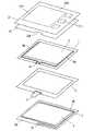
図1は本発明の一実施の形態によるタッチパネルの断面図、図2は同分解斜視図であり、同図において、1はポリエチレンテレフタレートやポリエーテルサルホン、ポリカーボネート等のフィルム状で光透過性の上基板、2は同じくフィルム状またはガラス等の薄板状で光透過性の下基板で、上基板1の下面には酸化インジウム錫や酸化錫等の光透過性の上導電層3が、下基板2の上面には同じく下導電層4が各々、スパッタ法等によって形成されている。(Embodiment)
FIG. 1 is a cross-sectional view of a touch panel according to an embodiment of the present invention, FIG. 2 is an exploded perspective view of the touch panel, in which 1 is a film of polyethylene terephthalate, polyethersulfone, polycarbonate, etc. The
また、上導電層3の前後端には銀やカーボン等の一対の上電極5Aと5Bが、下導電層4の上導電層3とは直交方向の左右端には、一対の下電極6Aと6Bが各々形成されると共に、この上電極5A、5Bや下電極6A、6Bが、上基板1や下基板2の外周左端の接続部1Aや2Aに延出している。 Further, a pair of
そして、下導電層4上面にはエポキシやシリコーン等の絶縁樹脂によって、複数のドットスペーサ(図示せず)が所定間隔で形成されると共に、上基板1と下基板2間の外周内縁には、略額縁状でポリエステルやエポキシ、不織布等のスペーサ7が設けられ、このスペーサ7の上下面または片面に塗布形成されたアクリルやゴム等の接着剤(図示せず)によって、上基板1と下基板2の外周が貼り合わされ、上導電層3と下導電層4が所定の間隙を空けて対向している。 A plurality of dot spacers (not shown) are formed at predetermined intervals on the upper surface of the lower
さらに、8はポリイミドやポリエチレンテレフタレート等のフィルム状の配線基板で、片面または上下面には銅箔や銀、カーボン等の複数の配線パターン9が形成されると共に、下面にはフィルム状のカバーシート10が貼付されて、左右端を除く複数の配線パターン9を覆っている。 Further, 8 is a film-like wiring board such as polyimide or polyethylene terephthalate, and a plurality of
そして、この配線基板8の右端が、上基板1と下基板2左端の接続部1Aや2Aの間に挟持され、エポキシやアクリル、ポリエステル等の合成樹脂内に、ニッケルや樹脂等に金メッキを施した複数の導電粒子を分散した異方導電接着剤(図示せず)等によって、各配線パターン9の右端が上電極5A、5Bや下電極6A、6Bに各々接着接続されている。 The right end of the
また、21はポリエチレンテレフタレート等のフィルム状の表示シートで、外形寸法が上基板1や下基板2よりもやや大きく、外周が上基板1や下基板2より外方へ突出するように形成されると共に、下面中央には透光部21Aや、この周囲の所定色に塗装された遮光部21B、文字等が印刷された操作部21Cが各々設けられている。
さらに、表示シート21下面にはアクリルやゴム等の接着層22が形成され、この接着層22によって表示シート21が上基板1上面に貼付されると共に、接続部1Aや2A上方の表示シート21下面には、接着層22が除かれ表示シート21下面が露出した非接着部22Aが設けられて、タッチパネルが構成されている。 Further, an
そして、このように構成されたタッチパネルが、液晶表示素子等の表示素子の前面に配置されて電子機器に装着されると共に、配線基板8の複数の配線パターン9の左端が、接続用コネクタや半田付け等によって機器の電子回路(図示せず)に電気的に接続される。 The touch panel thus configured is placed on the front surface of a display element such as a liquid crystal display element and attached to an electronic device, and the left ends of the plurality of
以上の構成において、タッチパネル背面の表示素子の表示に応じて、表示シート21の透光部21A上面や、あるいは操作部21C上面を指やペン等で押圧操作すると、この下方の上基板1が撓み、押圧された箇所の上導電層3が下導電層4に接触する。 In the above configuration, when the upper surface of the
そして、電子回路から配線基板8の複数の配線パターン9を介して、一対の上電極5A、5Bや下電極6A、6Bへ順次電圧が印加され、上導電層3両端、及びこれと直交方向の下導電層4両端の電圧比によって、押圧された箇所を電子回路が検出し、機器の様々な機能の切換えが行なわれる。 Then, a voltage is sequentially applied from the electronic circuit to the pair of
つまり、タッチパネル背面の表示素子に、例えば複数のメニュー等が表示された状態で、所望のメニュー上の透光部21Aや、あるいは操作部21Cを押圧操作すると、この操作した箇所を配線基板8の複数の配線パターン9を介して電子回路が検出して、複数のメニューの中から所望のメニューの選択や、あるいは確定等の操作が行えるように構成されている。 That is, when the
また、以上のようなタッチパネルを製作するには、先ず、下面に酸化インジウム錫等の上導電層3が形成された上基板1や、上面に下導電層4が形成された下基板2に、印刷等によって上電極5A、5Bや下電極6A、6Bを形成する。 In order to manufacture the touch panel as described above, first, an
そして、異方導電接着剤を塗布した配線基板8の右端を、接続部1Aと2Aの間に挟んだ状態で、上基板1と下基板2をスペーサ7によって、上導電層3と下導電層4が所定の空隙を空けて対向するように貼り合せる。 Then, with the right end of the
さらに、接続部1Aと2Aを加熱加圧して、配線基板8の配線パターン9を上電極5A、5Bや下電極6A、6Bに接着接続した後、下面に形成された接着層22によって、上基板1上面に表示シート21を貼付して、タッチパネルが完成する。 Further, the
また、このように接続部1Aと2Aを加熱加圧して配線基板8を接着接続する際、上基板1下面の上電極5Aや5B、下基板2上面の下電極6Aや6B、スペーサ7等の厚さ寸法のばらつきや、あるいは上電極5A、5Bや下電極6A、6Bが形成されている箇所と、これらが形成されていない箇所の厚さ寸法の違い等によって、上基板1左端の接続部1Aに膨らみや窪みが生じる場合がある。 Further, when the
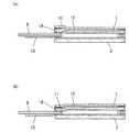
つまり、これらの厚さ寸法が大きな場合には、図3(a)の断面図に示すように、配線基板8右端を加熱加圧して接着接続した際、上基板1左端の接続部1Aに膨らみが生じてしまい、厚さ寸法が小さな場合には、図3(b)に示すように、上基板1左端の接続部1Aに窪みが生じてしまう。 That is, when these thickness dimensions are large, as shown in the cross-sectional view of FIG. 3A, when the right end of the
しかし、本発明においては、接続部1Aや2A上方の表示シート21下面には、接着層22が除かれ表示シート21下面が露出した非接着部22Aが設けられているため、上記のように上基板1左端の接続部1Aに膨らみや窪みが生じた場合でも、この上方の表示シート21左端には膨らみや窪みが発生しないように構成されている。 However, in the present invention, the lower surface of the
すなわち、下面の接着層22によって表示シート21は上基板1上面に貼付されているが、接続部1A上方の表示シート21下面には非接着部22Aが設けられ、接続部1A上面には接着されていないため、配線基板8の接着接続時に上基板1の接続部1Aに膨らみや窪みが生じても、この上方の表示シート21左端にはこれらが発生しないようになっている。 That is, the
したがって、各構成部品の厚さ寸法のばらつきや違い等によって、上基板1の接続部1Aに膨らみや窪みが生じた場合でも、表示シート11左端がうねったような状態となることはないため、透光部21Aを通したタッチパネル背面の表示素子の表示が見づらいものとなることもなく、見易く、容易に操作を行うことができる。 Accordingly, even if the connecting
なお、各構成部品の厚さ寸法のばらつきや違い等は個々の部品としては数μm前後のものであるが、これらが組み合わされた場合には10〜30μm前後となるため、接着層22の厚さを50μm前後に形成し、非接着部22Aによってこの程度の隙間を、表示シート11下面と接続部1A上面との間に設けることが好ましい。 In addition, although the dispersion | variation in thickness dimension of each component, a difference, etc. are about several micrometers as individual parts, when these are combined, it will be about 10-30 micrometers, Therefore The thickness of the
また、表示シート11の外形寸法を上基板1や下基板2よりもやや大きくし、外周が上基板1や下基板2よりも外方へ突出するように形成することで、この外周下面の接着層22によって、タッチパネルを機器の筐体に貼付装着することも可能となる。 Further, the outer dimensions of the
このように本実施の形態によれば、接続部1Aや2A上方の表示シート21下面に、接着層22が除かれた非接着部22Aを設けることで、配線基板8を接着接続する際、厚さ寸法のばらつきや違い等によって、上基板1の接続部1Aに膨らみや窪みが生じた場合でも、この上方の表示シート21には下面が露出した非接着部22Aが形成され、表示シート21には膨らみや窪みが発生しないため、見易く、容易な操作が可能なタッチパネルを得ることができるものである。 As described above, according to the present embodiment, when the
本発明によるタッチパネルは、見易く、容易な操作が可能なものを得ることができるという有利な効果を有し、主に各種電子機器の操作用として有用である。 The touch panel according to the present invention has an advantageous effect that an easy-to-see and easy-to-operate device can be obtained, and is mainly useful for operation of various electronic devices.
1 上基板
1A、2A 接続部
2 下基板
3 上導電層
4 下導電層
5A、5B 上電極
6A、6B 下電極
7 スペーサ
8 配線基板
9 配線パターン
10 カバーシート
21 表示シート
21A 透光部
21B 遮光部
21C 操作部
22 接着層
22A 非接着部DESCRIPTION OF
Claims (1)
Translated fromJapanesePriority Applications (3)
| Application Number | Priority Date | Filing Date | Title |
|---|---|---|---|
| JP2010118006AJP5531778B2 (en) | 2010-05-24 | 2010-05-24 | Touch panel |
| US13/105,078US8735730B2 (en) | 2010-05-24 | 2011-05-11 | Touch panel and method of manufacturing the same |
| CN201110139251.4ACN102262480B (en) | 2010-05-24 | 2011-05-23 | Touch panel and method of manufacturing the same |
Applications Claiming Priority (1)
| Application Number | Priority Date | Filing Date | Title |
|---|---|---|---|
| JP2010118006AJP5531778B2 (en) | 2010-05-24 | 2010-05-24 | Touch panel |
Publications (2)
| Publication Number | Publication Date |
|---|---|
| JP2011248426A JP2011248426A (en) | 2011-12-08 |
| JP5531778B2true JP5531778B2 (en) | 2014-06-25 |
Family
ID=44972121
Family Applications (1)
| Application Number | Title | Priority Date | Filing Date |
|---|---|---|---|
| JP2010118006AActiveJP5531778B2 (en) | 2010-05-24 | 2010-05-24 | Touch panel |
Country Status (3)
| Country | Link |
|---|---|
| US (1) | US8735730B2 (en) |
| JP (1) | JP5531778B2 (en) |
| CN (1) | CN102262480B (en) |
Families Citing this family (7)
| Publication number | Priority date | Publication date | Assignee | Title |
|---|---|---|---|---|
| US6587093B1 (en)* | 1999-11-04 | 2003-07-01 | Synaptics Incorporated | Capacitive mouse |
| JP5407599B2 (en)* | 2009-07-01 | 2014-02-05 | パナソニック株式会社 | Touch panel |
| US9092082B2 (en)* | 2010-12-22 | 2015-07-28 | Synaptics Incorporated | Methods and apparatus for mounting a touch sensor device |
| TW201303659A (en)* | 2011-07-07 | 2013-01-16 | Wintek Corp | Touch-sensitive display panel |
| CN103677368B (en)* | 2012-09-20 | 2016-11-23 | 瀚宇彩晶股份有限公司 | Bonding structure of touch panel and flexible circuit board |
| WO2014208445A1 (en)* | 2013-06-27 | 2014-12-31 | 東レ株式会社 | Electroconductive paste, method for manufacturing an electroconductive pattern, and touch panel |
| CN107851646A (en)* | 2015-07-10 | 2018-03-27 | 凸版印刷株式会社 | Wiring substrate and its manufacture method |
Family Cites Families (9)
| Publication number | Priority date | Publication date | Assignee | Title |
|---|---|---|---|---|
| US6958748B1 (en)* | 1999-04-20 | 2005-10-25 | Matsushita Electric Industrial Co., Ltd. | Transparent board with conductive multi-layer antireflection films, transparent touch panel using this transparent board with multi-layer antireflection films, and electronic equipment with this transparent touch panel |
| US8400430B2 (en)* | 2003-11-21 | 2013-03-19 | American Panel Corporation | Display device with integral touch panel surface |
| JP4591157B2 (en) | 2005-03-31 | 2010-12-01 | パナソニック株式会社 | Wiring board, input device using the same, and manufacturing method thereof |
| JP4821290B2 (en)* | 2005-12-01 | 2011-11-24 | パナソニック株式会社 | Touch panel |
| TW200846993A (en)* | 2007-03-26 | 2008-12-01 | Nissha Printing | Protective panel with touch input function of electronic instrument display window |
| CN201111008Y (en) | 2007-10-29 | 2008-09-03 | 洋华光电股份有限公司 | Bus cable package assembly of touching control panel |
| JP5098798B2 (en)* | 2008-05-16 | 2012-12-12 | パナソニック株式会社 | Touch panel and input device using the same |
| CN101598984A (en) | 2008-06-02 | 2009-12-09 | 胜华科技股份有限公司 | Touch panel and touch display with same |
| JP5106341B2 (en) | 2008-10-02 | 2012-12-26 | 株式会社ジャパンディスプレイイースト | Display device |
- 2010
- 2010-05-24JPJP2010118006Apatent/JP5531778B2/enactiveActive
- 2011
- 2011-05-11USUS13/105,078patent/US8735730B2/ennot_activeExpired - Fee Related
- 2011-05-23CNCN201110139251.4Apatent/CN102262480B/enactiveActive
Also Published As
| Publication number | Publication date |
|---|---|
| US20110285655A1 (en) | 2011-11-24 |
| CN102262480B (en) | 2014-10-22 |
| US8735730B2 (en) | 2014-05-27 |
| CN102262480A (en) | 2011-11-30 |
| JP2011248426A (en) | 2011-12-08 |
Similar Documents
| Publication | Publication Date | Title |
|---|---|---|
| JP4779681B2 (en) | Touch panel | |
| JP5531778B2 (en) | Touch panel | |
| JP5194496B2 (en) | Touch panel | |
| JP4539241B2 (en) | Touch panel and manufacturing method thereof | |
| US20090284487A1 (en) | Touch panel and input device using same | |
| US8803830B2 (en) | Touch panel with conductive layers formed of parallel strips | |
| JP2012048279A (en) | Input device | |
| US7746662B2 (en) | Touch panel | |
| CN101639745A (en) | Touch panel and display unit | |
| JP4893082B2 (en) | Touch panel | |
| JP2007233513A (en) | Touch panel | |
| JP2014026496A (en) | Touch panel | |
| JP2003108302A (en) | Transparent touch panel | |
| JP2010055347A (en) | Touch panel and input device using the same | |
| JP2014112356A (en) | Touch panel | |
| JP2010191741A (en) | Touch panel | |
| JP2012059091A (en) | Touch panel | |
| JP5581800B2 (en) | Wiring board and touch panel using the same | |
| JP2013250836A (en) | Touch panel | |
| JP5093018B2 (en) | Input device | |
| JP2012088822A (en) | Touch panel | |
| JP2014093010A (en) | Touch panel | |
| JP4013511B2 (en) | Transparent touch panel | |
| JP2011065407A (en) | Touch panel | |
| JP2011113453A (en) | Touch panel |
Legal Events
| Date | Code | Title | Description |
|---|---|---|---|
| A621 | Written request for application examination | Free format text:JAPANESE INTERMEDIATE CODE: A621 Effective date:20130515 | |
| RD01 | Notification of change of attorney | Free format text:JAPANESE INTERMEDIATE CODE: A7421 Effective date:20130612 | |
| A977 | Report on retrieval | Free format text:JAPANESE INTERMEDIATE CODE: A971007 Effective date:20131225 | |
| A131 | Notification of reasons for refusal | Free format text:JAPANESE INTERMEDIATE CODE: A131 Effective date:20140107 | |
| RD01 | Notification of change of attorney | Free format text:JAPANESE INTERMEDIATE CODE: A7421 Effective date:20140107 | |
| A521 | Written amendment | Free format text:JAPANESE INTERMEDIATE CODE: A523 Effective date:20140303 | |
| TRDD | Decision of grant or rejection written | ||
| A01 | Written decision to grant a patent or to grant a registration (utility model) | Free format text:JAPANESE INTERMEDIATE CODE: A01 Effective date:20140325 | |
| A61 | First payment of annual fees (during grant procedure) | Free format text:JAPANESE INTERMEDIATE CODE: A61 Effective date:20140407 | |
| R151 | Written notification of patent or utility model registration | Ref document number:5531778 Country of ref document:JP Free format text:JAPANESE INTERMEDIATE CODE: R151 |