JP5513927B2 - Semiconductor device and nonvolatile semiconductor memory device - Google Patents
Semiconductor device and nonvolatile semiconductor memory deviceDownload PDFInfo
- Publication number
- JP5513927B2 JP5513927B2JP2010040614AJP2010040614AJP5513927B2JP 5513927 B2JP5513927 B2JP 5513927B2JP 2010040614 AJP2010040614 AJP 2010040614AJP 2010040614 AJP2010040614 AJP 2010040614AJP 5513927 B2JP5513927 B2JP 5513927B2
- Authority
- JP
- Japan
- Prior art keywords
- insulating film
- conductive layer
- region
- contact plug
- element isolation
- Prior art date
- Legal status (The legal status is an assumption and is not a legal conclusion. Google has not performed a legal analysis and makes no representation as to the accuracy of the status listed.)
- Expired - Fee Related
Links
Images


Classifications
- H—ELECTRICITY
- H01—ELECTRIC ELEMENTS
- H01L—SEMICONDUCTOR DEVICES NOT COVERED BY CLASS H10
- H01L21/00—Processes or apparatus adapted for the manufacture or treatment of semiconductor or solid state devices or of parts thereof
- H01L21/70—Manufacture or treatment of devices consisting of a plurality of solid state components formed in or on a common substrate or of parts thereof; Manufacture of integrated circuit devices or of parts thereof
- H01L21/71—Manufacture of specific parts of devices defined in group H01L21/70
- H01L21/768—Applying interconnections to be used for carrying current between separate components within a device comprising conductors and dielectrics
- H01L21/76897—Formation of self-aligned vias or contact plugs, i.e. involving a lithographically uncritical step
- H—ELECTRICITY
- H10—SEMICONDUCTOR DEVICES; ELECTRIC SOLID-STATE DEVICES NOT OTHERWISE PROVIDED FOR
- H10D—INORGANIC ELECTRIC SEMICONDUCTOR DEVICES
- H10D30/00—Field-effect transistors [FET]
- H10D30/01—Manufacture or treatment
- H10D30/021—Manufacture or treatment of FETs having insulated gates [IGFET]
- H10D30/0411—Manufacture or treatment of FETs having insulated gates [IGFET] of FETs having floating gates
- H—ELECTRICITY
- H10—SEMICONDUCTOR DEVICES; ELECTRIC SOLID-STATE DEVICES NOT OTHERWISE PROVIDED FOR
- H10D—INORGANIC ELECTRIC SEMICONDUCTOR DEVICES
- H10D30/00—Field-effect transistors [FET]
- H10D30/60—Insulated-gate field-effect transistors [IGFET]
- H10D30/68—Floating-gate IGFETs
- H10D30/681—Floating-gate IGFETs having only two programming levels
- H—ELECTRICITY
- H10—SEMICONDUCTOR DEVICES; ELECTRIC SOLID-STATE DEVICES NOT OTHERWISE PROVIDED FOR
- H10D—INORGANIC ELECTRIC SEMICONDUCTOR DEVICES
- H10D30/00—Field-effect transistors [FET]
- H10D30/60—Insulated-gate field-effect transistors [IGFET]
- H10D30/68—Floating-gate IGFETs
- H10D30/6891—Floating-gate IGFETs characterised by the shapes, relative sizes or dispositions of the floating gate electrode
- H—ELECTRICITY
- H10—SEMICONDUCTOR DEVICES; ELECTRIC SOLID-STATE DEVICES NOT OTHERWISE PROVIDED FOR
- H10D—INORGANIC ELECTRIC SEMICONDUCTOR DEVICES
- H10D64/00—Electrodes of devices having potential barriers
- H10D64/01—Manufacture or treatment
- H10D64/031—Manufacture or treatment of data-storage electrodes
- H10D64/035—Manufacture or treatment of data-storage electrodes comprising conductor-insulator-conductor-insulator-semiconductor structures
Landscapes
- Engineering & Computer Science (AREA)
- Physics & Mathematics (AREA)
- Condensed Matter Physics & Semiconductors (AREA)
- General Physics & Mathematics (AREA)
- Manufacturing & Machinery (AREA)
- Computer Hardware Design (AREA)
- Microelectronics & Electronic Packaging (AREA)
- Power Engineering (AREA)
- Non-Volatile Memory (AREA)
- Semiconductor Memories (AREA)
- Semiconductor Integrated Circuits (AREA)
Description
Translated fromJapanese本発明は、2層ゲート構造のメモリセルと同一構造の積層構造を有する半導体装置及びこれを用いた不揮発性半導体憶装置に関する。 The present invention relates to a semiconductor device having a stacked structure having the same structure as a memory cell having a two-layer gate structure, and a nonvolatile semiconductor memory device using the same.
2層ゲート構造のメモリセルを有する不揮発性半導体記憶装置において、周辺回路部のキャパシタは、メモリセル部分と同様に、Si基板上にトンネル絶縁膜,浮遊ゲート電極,電極間絶縁膜,及び制御ゲート電極を有する積層膜を用いて形成されている。即ち、制御ゲート電極を層間絶縁膜により分離し、制御ゲート電極と浮遊ゲート電極を電気的に接続させた制御ゲート電極上に第1のコンタクトプラグを接続し、2層ゲート構造の制御ゲート電極上に第2のコンタクトプラグを接続し、Si基板に第3のコンタクトプラグを接続し、浮遊ゲートと制御ゲートとの間、浮遊ゲートと基板との間にそれぞれキャパシタを形成している。 In a nonvolatile semiconductor memory device having a memory cell having a two-layer gate structure, a capacitor in a peripheral circuit section is formed on a Si substrate with a tunnel insulating film, a floating gate electrode, an interelectrode insulating film, and a control gate, similar to the memory cell portion. It is formed using a laminated film having electrodes. That is, the control gate electrode is separated by the interlayer insulating film, the first contact plug is connected to the control gate electrode in which the control gate electrode and the floating gate electrode are electrically connected, and the control gate electrode on the two-layer gate structure is formed. The second contact plug is connected to the Si substrate, the third contact plug is connected to the Si substrate, and a capacitor is formed between the floating gate and the control gate, and between the floating gate and the substrate.
現在、制御ゲート電極には、Siと金属元素による金属間化合物が用いられている。特に、Niとの金属間化合物であるNiシリサイドは、低抵抗でかつシリサイド成長の活性化エネルギーが比較的高いことから、上記の制御ゲート電極として有望である。 Currently, an intermetallic compound of Si and a metal element is used for the control gate electrode. In particular, Ni silicide which is an intermetallic compound with Ni is promising as the control gate electrode because of its low resistance and relatively high activation energy for silicide growth.
しかし、この種のシリサイド電極は、高温での熱処理によって、多結晶のシリサイド結晶粒が凝集してしまい、構造及び組成の均一性が劣化してしまう場合がある。その結果、制御ゲート電極であるシリサイド電極が凝集して不均一に形成されると、制御ゲート電極上にコンタクトプラグを形成した際に、シリサイド未形成箇所の制御ゲート電極を突き抜けて、下層の電極間絶縁膜までコンタクトプラグが貫通してしまう。このため、制御ゲート電極と浮遊ゲート電極をショートさせるという問題がある。 However, in this type of silicide electrode, polycrystalline silicide crystal grains may aggregate due to heat treatment at a high temperature, and the uniformity of the structure and composition may deteriorate. As a result, if the silicide electrode that is the control gate electrode is aggregated and formed unevenly, when the contact plug is formed on the control gate electrode, the control gate electrode is penetrated through the control gate electrode where the silicide is not formed. The contact plug penetrates to the insulating film. For this reason, there is a problem that the control gate electrode and the floating gate electrode are short-circuited.
なお、浮遊ゲート電極と制御ゲート電極との間だけにキャパシタを作製する例では、素子分離領域の上方にコンタクトプラグを配置した構成が提案されている(例えば、特許文献1参照)。しかし、この特許文献1には、浮遊ゲート電極と基板との間にもキャパシタを作製し、基板側の第3のコンタクトプラグを如何にして引き出し、制御ゲート電極への第2のコンタクトプラグに接続することは何ら開示されていない。さらに、シリサイド電極の凝集による問題は全く認識されていない。 In an example in which a capacitor is formed only between the floating gate electrode and the control gate electrode, a configuration in which a contact plug is disposed above the element isolation region has been proposed (see, for example, Patent Document 1). However, in Patent Document 1, a capacitor is also formed between the floating gate electrode and the substrate, and the third contact plug on the substrate side is drawn out and connected to the second contact plug to the control gate electrode. Nothing to do is disclosed. Furthermore, the problem due to the aggregation of silicide electrodes is not recognized at all.
本発明の目的は、キャパシタのコンタクトプラグ形成に伴うショート不良を低減させることができ、素子信頼性の向上をはかり得る半導体装置及び不揮発性半導体記憶装置を提供することにある。 An object of the present invention is to provide a semiconductor device and a nonvolatile semiconductor memory device that can reduce short-circuit defects caused by formation of contact plugs of capacitors and can improve element reliability.
本発明の一態様に係わる半導体装置は、半導体基板上に、第1の絶縁膜,第1の導電層,第2の絶縁膜,及び第2の導電層を上記順に積層して形成され、且つ第2の絶縁膜に形成された溝を介して第1及び第2の導電層が電気的に接続された積層構造部と、前記積層構造部の第2の導電層を、前記溝を含む面積の狭い第1の領域と前記溝を含まない面積の広い第2の領域に電気的に分離するように設けられた層間絶縁膜と、前記積層構造部の前記第2の領域側の一周辺部で、前記第1の導電層,前記第1の絶縁膜,及び前記半導体基板の一部に形成された第1の素子分離溝と、前記第1の素子分離溝に埋め込まれ、且つ、その上部に前記第1の導電層を介さず、前記第2の絶縁膜を介して前記第2の導電層が形成された第1の素子分離絶縁膜と、前記第2の導電層の第1の領域に接続された第1のコンタクトプラグと、前記第2の導電層の第2の領域に接続され、且つ前記第1の素子分離絶縁膜の上方に形成された第2のコンタクトプラグと、前記積層構造部の前記第2の領域側の一周辺部に隣接する領域で前記半導体基板に接続された第3のコンタクトプラグと、を具備してなることを特徴とする。A semiconductor device according to one embodiment of the present invention is formed by stacking a first insulating film, a first conductive layer, a second insulating film, and a second conductive layer in this order on a semiconductor substrate; and A laminated structure part in which the first and second conductive layers are electrically connected via a groove formed in the second insulating film, and an area including the groove, the second conductive layer of the laminated structure part An interlayer insulating film provided so as to be electrically separated into a narrow first region and a second region having a large area not including the trench, and one peripheral portion on the second region side of the stacked structure portion The first conductive layer, the first insulating film, the first element isolation groove formed in a part of the semiconductor substrate, the first element isolation groove, and the upper part thereof the first without the intervention of the conductive layer, the second first element isolation insulatingfilm via said insulating film a second conductive layer formed on , A first contact plug connected to the first region of the second conductive layer, and a second contact region connected to the second region of the second conductive layer and above the first element isolation insulating film. A second contact plug formed; and a third contact plug connected to the semiconductor substrate in a region adjacent to one peripheral portion of the stacked structure portion on the second region side. It is characterized by.
また、本発明の別の一態様に係わる半導体装置は、半導体基板上に、第1の絶縁膜,第1の導電層,第2の絶縁膜,及び第2の導電層を上記順に積層して形成され、且つ第2の絶縁膜に形成された溝を介して第1及び第2の導電層が電気的に接続された積層構造部と、前記積層構造部の第2の導電層を、前記溝を含む面積の狭い第1の領域と前記溝を含まない面積の広い第2の領域に電気的に分離するように設けられた層間絶縁膜と、前記積層構造部の前記第2の領域側の一周辺部で、前記第1の導電層,前記第1の絶縁膜及び前記半導体基板の一部に形成された素子分離溝と、前記素子分離溝に埋め込まれ、且つ、その上部に前記第1の導電層を介さず、前記第2の絶縁膜を介して前記第2の導電層が形成された素子分離絶縁膜と、前記第2の導電層の第1の領域に接続された第1のコンタクトプラグと、前記第2の導電層の第2の領域に接続され、且つ前記素子分離絶縁膜の上方に形成された第2のコンタクトプラグと、前記積層構造部の前記一周辺部とは異なる周辺部に隣接する領域で前記半導体基板に接続された第3のコンタクトプラグと、を具備してなることを特徴とする。In addition, a semiconductor device according to another embodiment of the present invention includes a first insulating film, a first conductive layer, a second insulating film, and a second conductive layer, which are stacked in this order on a semiconductor substrate. A laminated structure part formed and electrically connected to the first and second conductive layers through a groove formed in the second insulating film, and a second conductive layer of the laminated structure part, An interlayer insulating film provided so as to be electrically separated into a first region having a small area including a groove and a second region having a large area not including the groove; and the second region side of the stacked structure portion An element isolation trench formed in a part of the first conductive layer, the first insulating film, and the semiconductor substrate, and embedded in the element isolation trench, and on the upper portion, the first isolation layer without passing through the first conductive layer, said second conductive layer is formed an element isolation insulating filmvia the second insulating film, said first A first contact plug connected to the first region of the conductive layer, and a second contact connected to the second region of the second conductive layer and formed above the element isolation insulating film And a third contact plug connected to the semiconductor substrate in a region adjacent to a peripheral portion different from the one peripheral portion of the stacked structure portion.
また、本発明の別の一態様に係わる半導体装置は、半導体基板上に、第1の絶縁膜,第1の導電層,第2の絶縁膜,及び第2の導電層を上記順に積層して形成され、且つ第2の絶縁膜に形成された溝を介して第1及び第2の導電層が電気的に接続された積層構造部と、前記積層構造部の第2の導電層を、前記溝を含む面積の狭い第1の領域と前記溝を含まない面積の広い第2の領域に電気的に分離するように設けられた第1の層間絶縁膜と、前記第2の導電層の第1の領域に接続された第1のコンタクトプラグと、前記第2の導電層の第2の領域の一周辺部に接続された第2のコンタクトプラグと、前記積層構造部の前記一周辺部に隣接する領域で前記半導体基板に接続された第3のコンタクトプラグと、前記積層構造部の前記第2のコンタクトプラグと前記第1の層間絶縁膜との間で、前記第2の導電層の一部に埋め込み形成された第2の層間絶縁膜と、を具備してなることを特徴とする。In addition, a semiconductor device according to another embodiment of the present invention includes a first insulating film, a first conductive layer, a second insulating film, and a second conductive layer, which are stacked in this order on a semiconductor substrate. A laminated structure part formed and electrically connected to the first and second conductive layers through a groove formed in the second insulating film, and a second conductive layer of the laminated structure part, A first interlayer insulating film provided so as to be electrically separated into a first region having a small area including a groove and a second region having a large area not including the groove; and a first region of the second conductive layer. A first contact plug connected to one region, a second contact plug connected to one peripheral portion of the second region of the second conductive layer, and the one peripheral portion of the stacked structure portion A third contact plug connected to the semiconductor substrate in an adjacent region; and the second contour of the stacked structure portion. Between the the plugging first interlayer insulatingfilm, a second interlayer insulating film formed embedded inpart of theprevious SL second conductive layer, characterized by comprising comprises a.
また、本発明の別の一態様は、半導体基板上に不揮発性メモリセル部と周辺回路部を有し、周辺回路部にキャパシタを設けた不揮発性半導体記憶装置であって、前記周辺回路部のキャパシタは、前記半導体基板上に、トンネル絶縁膜,浮遊ゲート電極,電極間絶縁膜,及び制御ゲート電極を上記順に積層して形成され、且つ電極間絶縁膜に形成された溝を介して浮遊ゲート電極と制御ゲート電極が電気的に接続された積層構造部と、前記積層構造部の制御ゲート電極を、前記溝を含む面積の狭い第1の領域と前記溝を含まない面積の広い第2の領域に電気的に分離するように設けられた層間絶縁膜と、前記積層構造部の前記第2の領域側の一周辺部で、前記浮遊ゲート電極,前記トンネル絶縁膜及び前記半導体基板の一部に形成された素子分離溝と、前記素子分離溝に埋め込まれ、且つ、その上部に前記浮遊ゲート電極を介さず、前記電極間絶縁膜を介して前記制御ゲート電極が形成された素子分離絶縁膜と、前記制御ゲート電極の第1の領域に接続された第1のコンタクトプラグと、前記制御ゲート電極の第2の領域に接続され、且つ前記素子分離絶縁膜の上方に形成された第2のコンタクトプラグと、前記積層構造部の前記第2の領域側の一周辺部に隣接する領域で前記半導体基板に接続された第3のコンタクトプラグと、を具備してなることを特徴とする。Another embodiment of the present invention is a nonvolatile semiconductor memory device that includes a nonvolatile memory cell portion and a peripheral circuit portion on a semiconductor substrate, and includes a capacitor in the peripheral circuit portion. The capacitor is formed by laminating a tunnel insulating film, a floating gate electrode, an interelectrode insulating film, and a control gate electrode in the above order on the semiconductor substrate, and through the groove formed in the interelectrode insulating film, the floating gate A stacked structure portion in which an electrode and a control gate electrode are electrically connected; a control gate electrode of the stacked structure portion; a first region having a small area including the groove; and a second area having a large area not including the groove An interlayer insulating film provided so as to be electrically separated into a region, and a part of the semiconductor substrate, thefloating gate electrode , thetunnel insulating film, and one peripheral portion of the stacked structure portion on the second region side Element formed in A groove, buried in the device isolationtrench, and, without passing through the floating gate electrode thereon, and the element isolation insulatingfilm and the control gate electrode through the insulating film is formed, the control gate electrode A first contact plug connected to the first region, a second contact plug connected to the second region of the control gate electrode and formed above the element isolation insulating film, and the stacked layer And a third contact plug connected to the semiconductor substrate in a region adjacent to one peripheral portion of the structure portion on the second region side.
本発明によれば、キャパシタのコンタクトプラグ形成に伴うショート不良を低減させることができ、素子信頼性の向上をはかることができる。 According to the present invention, it is possible to reduce short-circuit defects associated with the formation of capacitor contact plugs and improve device reliability.
以下、本発明の詳細を図示の実施形態によって説明する。 The details of the present invention will be described below with reference to the illustrated embodiments.
(第1の実施形態)
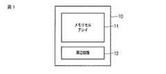
図1は、本発明の第1の実施形態に係わる不揮発性半導体記憶装置の基本構成を示すブロック図である。(First embodiment)
FIG. 1 is a block diagram showing a basic configuration of a nonvolatile semiconductor memory device according to the first embodiment of the present invention.
Si基板(半導体基板)10上に、メモリセルアレイ(メモリセル部)11と、各種トランジスタ及びキャパシタを設けた周辺回路部12が配置されている。メモリセルアレイ11は、浮遊ゲートと制御ゲートを有する2層ゲート構成の不揮発性メモリセルを複数個直列接続したNANDセルユニットをアレイ配置したものである。周辺回路部12のトランジスタやキャパシタは、製造プロセスの簡略化から、メモリセルのゲート構成と同じ構成となっている。 On a Si substrate (semiconductor substrate) 10, a memory cell array (memory cell unit) 11 and a
周辺回路部12のキャパシタは、図2及び図3(a)(b)に示すように構成されている。図2は、本実施形態に用いたゲート積層構造を有するキャパシタの概略構成を示す平面図であり、図3(a)は図2の矢視A−A’断面図、図3(b)は図2の矢視B−B’断面図である。 The capacitor of the
Si基板(半導体基板)10上の一部に、シリコン酸化膜等からなるトンネル絶縁膜(第1の絶縁膜)21を介して、ポリSi等からなる浮遊ゲート電極(第1の導電層)22が形成されている。浮遊ゲート電極22及びトンネル絶縁膜21の右側の端部と基板10の一部をエッチングして溝が形成され、この溝内にシリコン酸化膜等からなる素子分離絶縁膜(第1の素子分離絶縁膜)15が埋め込み形成されている。ここで、素子分離絶縁膜15は、図2の平面図から分かるように、Y方向に連続的に形成されるのではなく、Y方向に分離して複数箇所に形成されている。これにより、浮遊ゲート電極22の右側端部では、Y方向に沿って浮遊ゲート電極22と素子分離絶縁膜15が交互に配置されることになる。さらに、浮遊ゲート電極22の形成領域よりも右側では、Y方向に沿って基板表面が露出する部分と素子分離絶縁膜15が交互に配置されることになる。 A floating gate electrode (first conductive layer) 22 made of poly-Si or the like via a tunnel insulating film (first insulating film) 21 made of a silicon oxide film or the like on a part of the Si substrate (semiconductor substrate) 10. Is formed. A groove is formed by etching the right end of the
浮遊ゲート電極22及び素子分離絶縁膜15上の一部には、電極間絶縁膜(第2の絶縁膜)23を介して制御ゲート電極(第2の導電層)24が形成されている。電極間絶縁膜23としてはトンネル絶縁膜よりも誘電率の高いシリコン窒化膜や酸化膜/窒化膜/酸化膜の積層構造(ONO膜)を用いることができる。制御ゲート電極24としては金属シリサイドを用いることができるが、特にNiシリサイドが適している。 A control gate electrode (second conductive layer) 24 is formed on part of the
なお、トンネル絶縁膜21,浮遊ゲート電極22,電極間絶縁膜23,及び制御ゲート電極24からなる積層構造部は、図2に示すように、矩形状に形成されている。そして、積層構造部の右側の端部では、浮遊ゲート22及びトンネル絶縁膜21が凹凸形状を有するものとなっている。 Note that the laminated structure portion including the
制御ゲート電極24の中央部よりも左側の位置に該ゲート電極24を左側の第1の領域51と右側の第2の領域52とに分離するように溝が形成され、この溝内に層間絶縁膜(第1の層間絶縁膜)26が形成されている。層間絶縁膜26よりも左側の位置、即ち第1の領域51で電極間絶縁膜23の一部を除去して開口部(接続部)25が形成され、この開口部25で浮遊ゲート電極22と制御ゲート電極24が電気的に接続されている。 A groove is formed at a position on the left side of the central portion of the
制御ゲート電極24には、層間絶縁膜26よりも左側の位置、即ち第1の領域51で且つ電極間絶縁膜23を除去した部分の上方に複数の第1のコンタクトプラグ31が接続され、層間絶縁膜26よりも右側の位置、即ち第2の領域52で且つ素子分離絶縁膜15の上方に位置する部分に複数の第2のコンタクトプラグ32が接続されている。そして、Si基板10には、積層構造部の右側端部に隣接し、且つ素子分離絶縁膜15に隣接する位置で複数の第3のコンタクトプラグ33が接続されている。第1〜第3のコンタクトプラグ31〜33の配列方向は共にX方向となっている。 A plurality of
このような構成であれば、第2のコンタクトプラグ32を素子分離絶縁膜15の上方に形成させることによって、コンタクトプラグ32が電極間絶縁膜23を突き抜けたとしても制御ゲート電極24と浮遊ゲート電極22間のショートを回避できる。即ち、キャパシタのコンタクトプラグの配置及びコンタクトプラグ下層の構造を変更することによって、コンタクト形成時に発生するショートを防止することができる。従って、素子信頼性の向上をはかることができる。 With such a configuration, by forming the
この効果をより詳しく説明すると次の通りである。制御ゲート電極24としてNiシリサイドを用いる場合、電極間絶縁膜23の上にポリSi膜を堆積し、その上にNi膜を堆積した後、熱処理を施してシリサイド化することによりNiシリサイドを形成する。このとき、高温での熱処理によって、多結晶のシリサイド結晶粒が凝集してしまい、構造及び組成の均一性が劣化してしまい、制御ゲート電極24であるシリサイド電極が凝集して不均一に形成される場合がある。そして、制御ゲート電極24上にコンタクトプラグ32を形成した際に、シリサイド未形成箇所の制御ゲート電極24を突き抜けて、下層の電極間絶縁膜23までコンタクトプラグ32が貫通し、制御ゲート電極24と浮遊ゲート電極22をショートさせるおそれがある。 This effect will be described in more detail as follows. When Ni silicide is used as the
これに対し本実施形態では、第2のコンタクトプラグ32を素子分離絶縁膜15の上方に形成しているため、仮に突き抜けが生じても、制御ゲート電極24と浮遊ゲート電極22のショートを防止することができるのである。 On the other hand, in the present embodiment, since the
また、本実施形態では、第2のコンタクトプラグ32と第3のコンタクトプラグ33とは電気的に接続され、基板10と浮遊ゲート電極22との間に設けられるキャパシタと、制御ゲート電極24の第2の領域52と浮遊ゲート電極22との間に設けられるキャパシタとが並列接続され、キャパシタ容量の増大をはかることができる。さらに、本実施形態では、第2のコンタクトプラグ32と第3のコンタクトプラグ33が隣接しているため、これらを接続する配線を容易に形成することができる利点もある。 Further, in the present embodiment, the
なお、第2のコンタクトプラグ32と第3のコンタクトプラグ33の比率は必ずしも同じである必要はない。さらに、第1のコンタクトプラグ31と、第2及び第3のコンタクトプラグ32,33の比率も同じである必要はない。 The ratio of the
(第2の実施形態)
図4は、本発明の第2の実施形態に係わる不揮発性半導体記憶装置の要部構成を説明するためのもので、図4(a)は平面図、図4(b)は(a)の矢視A−A’断面図である。なお、図2及び図3と同一部分には同一符号を付して、その詳しい説明は省略する。(Second Embodiment)
FIGS. 4A and 4B are diagrams for explaining a main configuration of the nonvolatile semiconductor memory device according to the second embodiment of the present invention. FIG. 4A is a plan view, and FIG. 4B is a plan view of FIG. It is arrow AA 'sectional drawing. 2 and 3 are denoted by the same reference numerals, and detailed description thereof is omitted.
本実施形態が先に説明した第1の実施形態と異なる点は、第2のコンタクトプラグ32側のみではなく、第1のコンタクトプラグ31側にも素子分離絶縁膜(第2の素子分離絶縁膜)35を設けたことにある。即ち、浮遊ゲート電極22及びトンネル絶縁膜21の左側の端部と基板10の一部をエッチングして溝が形成され、この溝内に素子分離絶縁膜35が埋め込み形成されている。そして、コンタクトプラグ31は素子分離絶縁膜35の上方に位置するようになっている。 This embodiment is different from the first embodiment described above in that not only the
ここで、素子分離絶縁膜35は、素子分離絶縁膜15と同時に形成された同じ材料であり、図4(a)の平面図から分かるように、Y方向に連続的して形成されている。また、電極間絶縁膜23を一部除去する部分は、素子分離絶縁膜35の上方を避けて設けられている。 Here, the element
このような構成であれば、先の第1の実施形態と同様の効果が得られるのは勿論のこと、第1のコンタクトプラグ31を素子分離絶縁膜35の上方に形成することによって、コンタクトプラグ31の突き抜けが生じても、浮遊ゲート電極22と半導体基板10との間のショートを回避することができる。従って、第2のコンタクトプラグ32だけでなく、第1のコンタクトプラグ31,32の突き抜けによる問題を解決することができ、更なる信頼性の向上をはかることができる。 With such a configuration, the same effects as those of the first embodiment can be obtained, and the contact plug can be obtained by forming the
(第3の実施形態)
図5は、本発明の第3の実施形態に係わる不揮発性半導体記憶装置の要部構成を説明するためのもので、図5(a)は平面図、図5(b)は(a)の矢視A−A’断面図である。なお、図2及び図3と同一部分には同一符号を付して、その詳しい説明は省略する。(Third embodiment)
FIGS. 5A and 5B are diagrams for explaining a main configuration of a nonvolatile semiconductor memory device according to the third embodiment of the present invention. FIG. 5A is a plan view and FIG. 5B is a plan view of FIG. It is arrow AA 'sectional drawing. 2 and 3 are denoted by the same reference numerals, and detailed description thereof is omitted.
本実施形態が先に説明した第1の実施形態と異なる点は、第2のコンタクトプラグ32及び第3のコンタクトプラグ33の形成位置である。 The difference between the present embodiment and the first embodiment described above is the formation positions of the
本実施形態では、制御ゲート電極24及び電極間絶縁膜23の一周辺部(図5(a)の下辺部)が図示しない素子分離絶縁膜上まで延在して設けられ、この部分に第2のコンタクトプラグ32が形成されている。 In the present embodiment, one peripheral portion (the lower side portion of FIG. 5A) of the
また、積層構造部の右側の辺は、浮遊ゲート電極22及びトンネル絶縁膜21が凹凸状に除去されるのではなく、制御ゲート電極24及び電極間絶縁膜23と同様にほぼ直線となっている。そして、積層構造部の右側の辺に隣接する領域でSi基板10に第3のコンタクトプラグ33が接続されている。また、第1のコンタクトプラグ31は第1の実施形態と同様に、制御ゲート電極24の第1の領域51に接続されている。ここで、第2の実施形態のように、第2の領域52側にも素子分離絶縁膜35を設け、第1のコンタクトプラグ31を素子分離絶縁膜35の上方に形成するようにしても良い。 In addition, the floating
このように本実施形態によれば、第2のコンタクトプラグ32をキャパシタ端の素子分離領域上に形成することによって、第1の実施形態と同様に、コンタクトプラグ32が電極間絶縁膜23を突き抜けたとしても、制御ゲート電極24と浮遊ゲート電極22との間のショートを未然に回避することができる。従って、第1の実施形態と同様の効果が得られる。 As described above, according to the present embodiment, the
なお、本実施形態では、第2のコンタクトプラグ32と第3のコンタクトプラグ33とを互いに垂直方向となる別の辺に形成することによって、コンタクトプラグ形成後の配線工程が従来構造に比べて複雑になる可能性がある。しかし、第2のコンタクトプラグ32及び第3のコンタクトプラグ33の数を間引くことなく、第2のコンタクトプラグ32を素子分離領域上に形成することができ、コンタクト抵抗の低減をはかり得ると云う利点がある。 In the present embodiment, the
(第4の実施形態)
図6は、本発明の第4の実施形態に係わる不揮発性半導体記憶装置の要部構成を説明するためもので、図6(a)は平面図、図6(b)は(a)の矢視A−A’断面図である。なお、図2及び図3と同一部分には同一符号を付して、その詳しい説明は省略する。(Fourth embodiment)
FIGS. 6A and 6B are diagrams for explaining a main configuration of a nonvolatile semiconductor memory device according to the fourth embodiment of the present invention. FIG. 6A is a plan view, and FIG. 6B is an arrow of FIG. It is view AA 'sectional drawing. 2 and 3 are denoted by the same reference numerals, and detailed description thereof is omitted.
本実施形態が先に説明した第3の実施形態と異なる点は、第2のコンタクトプラグ32の位置及び新たに層間絶縁膜(第2の層間絶縁膜)36を設けたことにある。 This embodiment is different from the third embodiment described above in that the position of the
即ち、第2のコンタクトプラグ32は、制御ゲート電極24の右側の周辺部に設けられている。ここで、積層構造部の右側の辺は、浮遊ゲート電極22及びトンネル絶縁膜21が凹凸状に除去されるのではなく、制御ゲート電極24及び電極間絶縁膜23と同様にほぼ直線となっている。そして、第2のコンタクトプラグ32と層間絶縁膜26との間で第2のコンタクトプラグ32の近傍位置で、制御ゲート電極24の一部に層間絶縁膜36が埋め込み形成されている。この層間絶縁膜36は、層間絶縁膜26とは異なり、Y方向に連続するのではなく断続的に設けられており、更に層間絶縁膜36の幅は層間絶縁膜26よりも狭くなっている。 That is, the
具体的には、制御ゲート電極24を形成する前に、電極間絶縁膜23上に層間絶縁膜としての絶縁膜を堆積し、この絶縁膜を所望パターンに加工することにより、層間絶縁膜26,36を同時に形成する。次いで、露出した電極間絶縁膜23上にポリSi膜及びNi膜を堆積した後に、熱処理を施すことによって、Niシリサイドからなる制御ゲート電極24を形成する。 Specifically, before the
ここで、制御ゲート電極24の一部或いは全てがシリサイドで形成されている場合、シリサイドは、電極形成膜厚や体積、熱工程など様々な要因によって凝集し、不良の一因となる。そこで、第2のコンタクトプラグ近傍のシリサイド形成体積を小さくすることで、その周辺のシリサイド凝集抑制が可能である。即ち、第2のコンタクトプラグ32を形成する制御ゲート24の一部を除去することによって、見かけ上、第2のコンタクトプラグ32に接続する制御ゲート電極24のシリサイドの体積を小さくし、シリサイドを均一に形成させることができる。その結果、第2のコンタクトプラグ32の突き抜けを抑制させることが可能となる。 Here, when part or all of the
このように本実施形態によれば、第2のコンタクトプラグ32の近傍の一部の制御ゲート電極24を層間絶縁膜36で埋め込むことによって、キャパシタ容量の減少を最低限にし、かつ第2のコンタクトプラグ32を形成する制御ゲート電極24を均一に形成させることが可能となる。このため、コンタクトプラグ32の制御ゲート電極24及び電極間絶縁膜23の貫通を回避することが可能となる。 As described above, according to the present embodiment, a part of the
また、本実施形態では、第3の実施形態と同様に、第2のコンタクトプラグ32及び第3のコンタクトプラグ33の数を間引くことなく形成することができるため、コンタクト抵抗の低減をはかり得ると云う利点がある。さらに、層間絶縁膜36の形成を層間絶縁膜26と同時に行うことにより、層間絶縁膜36の形成に伴う工程の複雑化を防止し得ると云う利点もある。 Further, in the present embodiment, as in the third embodiment, since the number of the second contact plugs 32 and the third contact plugs 33 can be formed without thinning out, the contact resistance can be reduced. There is an advantage. Furthermore, by forming the
(変形例)
なお、本発明は上述した各実施形態に限定されるものではない。基板は必ずしもSi基板に限るものではなく、メモリセルを形成可能な半導体基板であればよい。さらに、絶縁膜上にSi層を形成したSOI基板を用いることも可能である。(Modification)
The present invention is not limited to the above-described embodiments. The substrate is not necessarily limited to the Si substrate, and may be any semiconductor substrate capable of forming memory cells. Furthermore, an SOI substrate in which a Si layer is formed on an insulating film can be used.
また、第1〜第3のコンタクトプラグの個数は必ずしも複数である必要はなく、十分なコンタクトが取れる条件であれば、それぞれ1つにすることも可能である。 Further, the number of first to third contact plugs is not necessarily plural, and can be one each as long as sufficient contact can be obtained.
メモリセル部を構成するメモリセルユニットは、NAND型に限らずOR型に適用することもできる。要は、メモリセルが浮遊ゲートと制御ゲートの2層ゲート構成を有する不揮発性半導体メモリセルであればよい。 The memory cell unit constituting the memory cell portion is not limited to the NAND type but can be applied to the OR type. In short, the memory cell may be a non-volatile semiconductor memory cell having a two-layer gate structure of a floating gate and a control gate.
また、実施形態では不揮発性半導体記憶装置を例にしたが、必ずしもこれに限らず、半導体基板上に第1の絶縁膜,第1の導電層,第2の絶縁膜,及び第2の導電層を積層した積層構造部を有する半導体装置であれば適用することが可能である。 In the embodiment, the nonvolatile semiconductor memory device is taken as an example. However, the present invention is not limited to this, and the first insulating film, the first conductive layer, the second insulating film, and the second conductive layer are not necessarily limited to this. The present invention can be applied to any semiconductor device having a stacked structure portion in which layers are stacked.
その他、本発明の要旨を逸脱しない範囲で、種々変形して実施することができる。 In addition, various modifications can be made without departing from the scope of the present invention.
10…Si基板(半導体基板)
11…メモリセルアレイ(メモリセル部)
12…周辺回路部
15…第1の素子分離絶縁膜
21…トンネル絶縁膜(第1の絶縁膜)
22…浮遊ゲート電極(第1の導電層)
23…電極間絶縁膜(第2の絶縁膜)
24…制御ゲート電極(第2の導電層)
26…第1の層間絶縁膜
31…第1のコンタクトプラグ
32…第2のコンタクトプラグ
33…第3のコンタクトプラグ
35…第2の素子分離絶縁膜
36…第2の層間絶縁膜
51…第1の領域
52…第2の領域10 ... Si substrate (semiconductor substrate)
11 ... Memory cell array (memory cell section)
DESCRIPTION OF
22: Floating gate electrode (first conductive layer)
23. Interelectrode insulating film (second insulating film)
24 ... Control gate electrode (second conductive layer)
26 ... first
Claims (5)
Translated fromJapanese前記積層構造部の第2の導電層を、前記溝を含む面積の狭い第1の領域と前記溝を含まない面積の広い第2の領域に電気的に分離するように設けられた層間絶縁膜と、
前記積層構造部の前記第2の領域側の一周辺部で、前記第1の導電層,前記第1の絶縁膜,及び前記半導体基板の一部に形成された第1の素子分離溝と、
前記第1の素子分離溝に埋め込まれ、且つ、その上部に前記第1の導電層を介さず、前記第2の絶縁膜を介して前記第2の導電層が形成された第1の素子分離絶縁膜と、
前記第2の導電層の第1の領域に接続された第1のコンタクトプラグと、
前記第2の導電層の第2の領域に接続され、且つ前記第1の素子分離絶縁膜の上方に形成された第2のコンタクトプラグと、
前記積層構造部の前記第2の領域側の一周辺部に隣接する領域で前記半導体基板に接続された第3のコンタクトプラグと、
を具備してなることを特徴とする半導体装置。A groove formed in the second insulating film is formed by laminating the first insulating film, the first conductive layer, the second insulating film, and the second conductive layer in the above order on the semiconductor substrate. A laminated structure portion in which the first and second conductive layers are electrically connected via each other;
An interlayer insulating film provided to electrically isolate the second conductive layer of the stacked structure portion into a first region having a small area including the groove and a second region having a large area not including the groove When,
A first element isolation trench formed in a part of the first conductive layer, the first insulating film, and the semiconductor substrate at one peripheral portion of the stacked structure portion on the second region side;
A first element isolation embedded in the first element isolation trench andhaving the second conductive layer formed thereon via the second insulating film without the first conductive layer interposed therebetween. An insulating film;
A first contact plug connected to the first region of the second conductive layer;
A second contact plug connected to the second region of the second conductive layer and formed above the first element isolation insulating film;
A third contact plug connected to the semiconductor substrate in a region adjacent to one peripheral portion of the stacked structure portion on the second region side;
A semiconductor device comprising:
前記第1のコンタクトプラグは、前記第2の素子分離絶縁膜の上方に形成されていることを特徴とする請求項1記載の半導体装置。A second element isolation groove formed in a part of the first conductive layer, the first insulating film, and the semiconductor substrate on the first region side of the stacked structure portion; and the second element. A second element isolation insulating film embedded inthe isolation trench andhaving the second conductive layer formed thereon via the second insulating film and not via the first conductive layer. And
2. The semiconductor device according to claim 1, wherein the first contact plug is formed above the second element isolation insulating film.
前記積層構造部の第2の導電層を、前記溝を含む面積の狭い第1の領域と前記溝を含まない面積の広い第2の領域に電気的に分離するように設けられた層間絶縁膜と、
前記積層構造部の前記第2の領域側の一周辺部で、前記第1の導電層,前記第1の絶縁膜及び前記半導体基板の一部に形成された素子分離溝と、
前記素子分離溝に埋め込まれ、且つ、その上部に前記第1の導電層を介さず、前記第2の絶縁膜を介して前記第2の導電層が形成された素子分離絶縁膜と、
前記第2の導電層の第1の領域に接続された第1のコンタクトプラグと、
前記第2の導電層の第2の領域に接続され、且つ前記素子分離絶縁膜の上方に形成された第2のコンタクトプラグと、
前記積層構造部の前記一周辺部とは異なる周辺部に隣接する領域で前記半導体基板に接続された第3のコンタクトプラグと、
を具備してなることを特徴とする半導体装置。A groove formed in the second insulating film is formed by laminating the first insulating film, the first conductive layer, the second insulating film, and the second conductive layer in the above order on the semiconductor substrate. A laminated structure portion in which the first and second conductive layers are electrically connected via each other;
An interlayer insulating film provided to electrically isolate the second conductive layer of the stacked structure portion into a first region having a small area including the groove and a second region having a large area not including the groove When,
An element isolation trench formed in a part of the first conductive layer, the first insulating film, and the semiconductor substrate at one peripheral portion of the stacked structure portion on the second region side;
An element isolationinsulating film embedded in the element isolation trench andhaving the second conductive layer formed thereon via the second insulating film without passing through the first conductive layer ;
A first contact plug connected to the first region of the second conductive layer;
A second contact plug connected to the second region of the second conductive layer and formed above the element isolation insulating film;
A third contact plug connected to the semiconductor substrate in a region adjacent to a peripheral portion different from the one peripheral portion of the stacked structure portion;
A semiconductor device comprising:
前記積層構造部の第2の導電層を、前記溝を含む面積の狭い第1の領域と前記溝を含まない面積の広い第2の領域に電気的に分離するように設けられた第1の層間絶縁膜と、
前記第2の導電層の第1の領域に接続された第1のコンタクトプラグと、
前記第2の導電層の第2の領域の一周辺部に接続された第2のコンタクトプラグと、
前記積層構造部の前記一周辺部に隣接する領域で前記半導体基板に接続された第3のコンタクトプラグと、
前記積層構造部の前記第2のコンタクトプラグと前記第1の層間絶縁膜との間で、前記第2の導電層の一部に埋め込み形成された第2の層間絶縁膜と、
を具備してなることを特徴とする半導体装置。A groove formed in the second insulating film is formed by laminating the first insulating film, the first conductive layer, the second insulating film, and the second conductive layer in the above order on the semiconductor substrate. A laminated structure portion in which the first and second conductive layers are electrically connected via each other;
The first conductive layer of the stacked structure part is provided so as to be electrically separated into a first area having a small area including the groove and a second area having a large area not including the groove. An interlayer insulating film;
A first contact plug connected to the first region of the second conductive layer;
A second contact plug connected to one peripheral portion of the second region of the second conductive layer;
A third contact plug connected to the semiconductor substrate in a region adjacent to the one peripheral portion of the stacked structure portion;
A second interlayer insulating film, wherein between the second contact plugs laminated structure portion and the first interlayer insulatingfilm, is buried inpart of theprevious SL second conductive layer,
A semiconductor device comprising:
前記半導体基板上に、トンネル絶縁膜,浮遊ゲート電極,電極間絶縁膜,及び制御ゲート電極を上記順に積層して形成され、且つ電極間絶縁膜に形成された溝を介して浮遊ゲート電極と制御ゲート電極が電気的に接続された積層構造部と、
前記積層構造部の制御ゲート電極を、前記溝を含む面積の狭い第1の領域と前記溝を含まない面積の広い第2の領域に電気的に分離するように設けられた層間絶縁膜と、
前記積層構造部の前記第2の領域側の一周辺部で、前記浮遊ゲート電極,前記トンネル絶縁膜及び前記半導体基板の一部に形成された素子分離溝と、
前記素子分離溝に埋め込まれ、且つ、その上部に前記浮遊ゲート電極を介さず、前記電極間絶縁膜を介して前記制御ゲート電極が形成された素子分離絶縁膜と、
前記制御ゲート電極の第1の領域に接続された第1のコンタクトプラグと、
前記制御ゲート電極の第2の領域に接続され、且つ前記素子分離絶縁膜の上方に形成された第2のコンタクトプラグと、
前記積層構造部の前記第2の領域側の一周辺部に隣接する領域で前記半導体基板に接続された第3のコンタクトプラグと、
を具備してなることを特徴とする不揮発性半導体記憶装置。A non-volatile semiconductor memory device having a non-volatile memory cell portion and a peripheral circuit portion on a semiconductor substrate, and a capacitor provided in the peripheral circuit portion, wherein the capacitor of the peripheral circuit portion is:
On the semiconductor substrate, a tunnel insulating film, a floating gate electrode, an interelectrode insulating film, and a control gate electrode are stacked in the above order, and are controlled with the floating gate electrode through a groove formed in the interelectrode insulating film. A laminated structure in which gate electrodes are electrically connected; and
An interlayer insulating film provided to electrically isolate the control gate electrode of the stacked structure portion into a first area having a small area including the groove and a second area having a large area not including the groove;
In one peripheral portion of the stacked structure portion on the second region side, thefloating gate electrode , thetunnel insulating film, and an element isolation trench formed in a part of the semiconductor substrate,
An element isolationinsulating film embedded in the element isolation trench andhaving the control gate electrode formed thereon via the inter-electrode insulating film without the floating gate electrode above ;
A first contact plug connected to the first region of the control gate electrode;
A second contact plug connected to the second region of the control gate electrode and formed above the element isolation insulating film;
A third contact plug connected to the semiconductor substrate in a region adjacent to one peripheral portion of the stacked structure portion on the second region side;
A non-volatile semiconductor memory device comprising:
Priority Applications (3)
| Application Number | Priority Date | Filing Date | Title |
|---|---|---|---|
| JP2010040614AJP5513927B2 (en) | 2010-02-25 | 2010-02-25 | Semiconductor device and nonvolatile semiconductor memory device |
| US12/871,362US8350312B2 (en) | 2010-02-25 | 2010-08-30 | Semiconductor device |
| KR1020100085934AKR101161090B1 (en) | 2010-02-25 | 2010-09-02 | Semiconductor device |
Applications Claiming Priority (1)
| Application Number | Priority Date | Filing Date | Title |
|---|---|---|---|
| JP2010040614AJP5513927B2 (en) | 2010-02-25 | 2010-02-25 | Semiconductor device and nonvolatile semiconductor memory device |
Publications (2)
| Publication Number | Publication Date |
|---|---|
| JP2011176227A JP2011176227A (en) | 2011-09-08 |
| JP5513927B2true JP5513927B2 (en) | 2014-06-04 |
Family
ID=44475775
Family Applications (1)
| Application Number | Title | Priority Date | Filing Date |
|---|---|---|---|
| JP2010040614AExpired - Fee RelatedJP5513927B2 (en) | 2010-02-25 | 2010-02-25 | Semiconductor device and nonvolatile semiconductor memory device |
Country Status (3)
| Country | Link |
|---|---|
| US (1) | US8350312B2 (en) |
| JP (1) | JP5513927B2 (en) |
| KR (1) | KR101161090B1 (en) |
Family Cites Families (5)
| Publication number | Priority date | Publication date | Assignee | Title |
|---|---|---|---|---|
| JP4008651B2 (en) | 2000-10-31 | 2007-11-14 | 株式会社東芝 | Semiconductor device and manufacturing method thereof |
| JP3947135B2 (en)* | 2003-05-30 | 2007-07-18 | 株式会社東芝 | Nonvolatile semiconductor memory device |
| JP2007049111A (en) | 2005-07-12 | 2007-02-22 | Toshiba Corp | Nonvolatile semiconductor memory device |
| JP4866652B2 (en) | 2006-05-10 | 2012-02-01 | ルネサスエレクトロニクス株式会社 | Semiconductor memory device |
| JP2008283134A (en) | 2007-05-14 | 2008-11-20 | Toshiba Corp | Semiconductor memory device and manufacturing method thereof |
- 2010
- 2010-02-25JPJP2010040614Apatent/JP5513927B2/ennot_activeExpired - Fee Related
- 2010-08-30USUS12/871,362patent/US8350312B2/enactiveActive
- 2010-09-02KRKR1020100085934Apatent/KR101161090B1/ennot_activeExpired - Fee Related
Also Published As
| Publication number | Publication date |
|---|---|
| KR101161090B1 (en) | 2012-06-29 |
| US20110204426A1 (en) | 2011-08-25 |
| US8350312B2 (en) | 2013-01-08 |
| KR20110097588A (en) | 2011-08-31 |
| JP2011176227A (en) | 2011-09-08 |
Similar Documents
| Publication | Publication Date | Title |
|---|---|---|
| US10804363B2 (en) | Three-dimensional semiconductor memory device and method of fabricating the same | |
| US9818757B2 (en) | Semiconductor device | |
| TWI578448B (en) | Semiconductor memory device and manufacturing method thereof | |
| TWI632668B (en) | Semiconductor device | |
| JP6228238B2 (en) | Nonvolatile memory cell having increased channel region effective width and method of manufacturing the same | |
| US11322515B2 (en) | Three-dimensional semiconductor devices | |
| CN104103641A (en) | NONVOLATILE MEMORY DEVICE and method of manufacturing the same | |
| JP2015028982A (en) | Non-volatile memory device and method of manufacturing the same | |
| TW201434114A (en) | Non-volatile semiconductor memory device and method of manufacturing same | |
| KR102733518B1 (en) | Semiconductor memory and method for forming the same | |
| US20160079269A1 (en) | Nonvolatile semiconductor memory device and method of manufacturing the same | |
| US20150325580A1 (en) | Semiconductor devices and methods of manufacturing the same | |
| KR20080097004A (en) | Nonvolatile Memory Device and Manufacturing Method Thereof | |
| JP2014187332A (en) | Nonvolatile storage device and method for manufacturing the same | |
| TWI512729B (en) | Semiconductor structure with improved capacitance of bit line | |
| JP2012204663A (en) | Semiconductor device and manufacturing method of the same | |
| JP5513927B2 (en) | Semiconductor device and nonvolatile semiconductor memory device | |
| TW201445705A (en) | Semiconductor device and method of manufacturing the same | |
| JP2010080498A (en) | Non-volatile semiconductor memory device and its manufacturing method | |
| TWI451533B (en) | Method of forming embedded flash memory | |
| JP2006186403A5 (en) | ||
| US20250287649A1 (en) | Integrated circuit semiconductor devices and methods of forming same | |
| JPS62165370A (en) | Non-volatile semiconductor memory device | |
| JP2013243177A (en) | Nonvolatile semiconductor storage device and manufacturing method of the same | |
| JP2009252773A (en) | Nonvolatile semiconductor memory device and manufacturing method thereof |
Legal Events
| Date | Code | Title | Description |
|---|---|---|---|
| A621 | Written request for application examination | Free format text:JAPANESE INTERMEDIATE CODE: A621 Effective date:20120305 | |
| A977 | Report on retrieval | Free format text:JAPANESE INTERMEDIATE CODE: A971007 Effective date:20130926 | |
| A131 | Notification of reasons for refusal | Free format text:JAPANESE INTERMEDIATE CODE: A131 Effective date:20131008 | |
| RD04 | Notification of resignation of power of attorney | Free format text:JAPANESE INTERMEDIATE CODE: A7424 Effective date:20131205 | |
| A521 | Request for written amendment filed | Free format text:JAPANESE INTERMEDIATE CODE: A523 Effective date:20131209 | |
| RD04 | Notification of resignation of power of attorney | Free format text:JAPANESE INTERMEDIATE CODE: A7424 Effective date:20131212 | |
| RD04 | Notification of resignation of power of attorney | Free format text:JAPANESE INTERMEDIATE CODE: A7424 Effective date:20131219 | |
| RD04 | Notification of resignation of power of attorney | Free format text:JAPANESE INTERMEDIATE CODE: A7424 Effective date:20131226 | |
| RD04 | Notification of resignation of power of attorney | Free format text:JAPANESE INTERMEDIATE CODE: A7424 Effective date:20140109 | |
| RD04 | Notification of resignation of power of attorney | Free format text:JAPANESE INTERMEDIATE CODE: A7424 Effective date:20140116 | |
| TRDD | Decision of grant or rejection written | ||
| A01 | Written decision to grant a patent or to grant a registration (utility model) | Free format text:JAPANESE INTERMEDIATE CODE: A01 Effective date:20140304 | |
| A61 | First payment of annual fees (during grant procedure) | Free format text:JAPANESE INTERMEDIATE CODE: A61 Effective date:20140328 | |
| LAPS | Cancellation because of no payment of annual fees |