JP5512515B2 - Light emitting device, surface light source, and liquid crystal display device - Google Patents
Light emitting device, surface light source, and liquid crystal display deviceDownload PDFInfo
- Publication number
- JP5512515B2 JP5512515B2JP2010514550AJP2010514550AJP5512515B2JP 5512515 B2JP5512515 B2JP 5512515B2JP 2010514550 AJP2010514550 AJP 2010514550AJP 2010514550 AJP2010514550 AJP 2010514550AJP 5512515 B2JP5512515 B2JP 5512515B2
- Authority
- JP
- Japan
- Prior art keywords
- light
- emitting device
- light emitting
- phosphor layer
- transparent resin
- Prior art date
- Legal status (The legal status is an assumption and is not a legal conclusion. Google has not performed a legal analysis and makes no representation as to the accuracy of the status listed.)
- Active
Links
Images


Classifications
- H—ELECTRICITY
- H10—SEMICONDUCTOR DEVICES; ELECTRIC SOLID-STATE DEVICES NOT OTHERWISE PROVIDED FOR
- H10H—INORGANIC LIGHT-EMITTING SEMICONDUCTOR DEVICES HAVING POTENTIAL BARRIERS
- H10H20/00—Individual inorganic light-emitting semiconductor devices having potential barriers, e.g. light-emitting diodes [LED]
- H10H20/80—Constructional details
- H10H20/85—Packages
- H10H20/852—Encapsulations
- H10H20/853—Encapsulations characterised by their shape
- G—PHYSICS
- G02—OPTICS
- G02B—OPTICAL ELEMENTS, SYSTEMS OR APPARATUS
- G02B6/00—Light guides; Structural details of arrangements comprising light guides and other optical elements, e.g. couplings
- G02B6/0001—Light guides; Structural details of arrangements comprising light guides and other optical elements, e.g. couplings specially adapted for lighting devices or systems
- G02B6/0011—Light guides; Structural details of arrangements comprising light guides and other optical elements, e.g. couplings specially adapted for lighting devices or systems the light guides being planar or of plate-like form
- G02B6/0013—Means for improving the coupling-in of light from the light source into the light guide
- G02B6/0023—Means for improving the coupling-in of light from the light source into the light guide provided by one optical element, or plurality thereof, placed between the light guide and the light source, or around the light source
- G—PHYSICS
- G02—OPTICS
- G02B—OPTICAL ELEMENTS, SYSTEMS OR APPARATUS
- G02B6/00—Light guides; Structural details of arrangements comprising light guides and other optical elements, e.g. couplings
- G02B6/0001—Light guides; Structural details of arrangements comprising light guides and other optical elements, e.g. couplings specially adapted for lighting devices or systems
- G02B6/0011—Light guides; Structural details of arrangements comprising light guides and other optical elements, e.g. couplings specially adapted for lighting devices or systems the light guides being planar or of plate-like form
- G02B6/0066—Light guides; Structural details of arrangements comprising light guides and other optical elements, e.g. couplings specially adapted for lighting devices or systems the light guides being planar or of plate-like form characterised by the light source being coupled to the light guide
- G02B6/0068—Arrangements of plural sources, e.g. multi-colour light sources
- H—ELECTRICITY
- H10—SEMICONDUCTOR DEVICES; ELECTRIC SOLID-STATE DEVICES NOT OTHERWISE PROVIDED FOR
- H10H—INORGANIC LIGHT-EMITTING SEMICONDUCTOR DEVICES HAVING POTENTIAL BARRIERS
- H10H20/00—Individual inorganic light-emitting semiconductor devices having potential barriers, e.g. light-emitting diodes [LED]
- H10H20/80—Constructional details
- H10H20/84—Coatings, e.g. passivation layers or antireflective coatings
- H—ELECTRICITY
- H10—SEMICONDUCTOR DEVICES; ELECTRIC SOLID-STATE DEVICES NOT OTHERWISE PROVIDED FOR
- H10H—INORGANIC LIGHT-EMITTING SEMICONDUCTOR DEVICES HAVING POTENTIAL BARRIERS
- H10H20/00—Individual inorganic light-emitting semiconductor devices having potential barriers, e.g. light-emitting diodes [LED]
- H10H20/80—Constructional details
- H10H20/85—Packages
- H10H20/851—Wavelength conversion means
- H—ELECTRICITY
- H10—SEMICONDUCTOR DEVICES; ELECTRIC SOLID-STATE DEVICES NOT OTHERWISE PROVIDED FOR
- H10H—INORGANIC LIGHT-EMITTING SEMICONDUCTOR DEVICES HAVING POTENTIAL BARRIERS
- H10H20/00—Individual inorganic light-emitting semiconductor devices having potential barriers, e.g. light-emitting diodes [LED]
- H10H20/80—Constructional details
- H10H20/85—Packages
- H10H20/855—Optical field-shaping means, e.g. lenses
- G—PHYSICS
- G02—OPTICS
- G02B—OPTICAL ELEMENTS, SYSTEMS OR APPARATUS
- G02B6/00—Light guides; Structural details of arrangements comprising light guides and other optical elements, e.g. couplings
- G02B6/0001—Light guides; Structural details of arrangements comprising light guides and other optical elements, e.g. couplings specially adapted for lighting devices or systems
- G02B6/0011—Light guides; Structural details of arrangements comprising light guides and other optical elements, e.g. couplings specially adapted for lighting devices or systems the light guides being planar or of plate-like form
- G02B6/0033—Means for improving the coupling-out of light from the light guide
- G02B6/005—Means for improving the coupling-out of light from the light guide provided by one optical element, or plurality thereof, placed on the light output side of the light guide
- G02B6/0055—Reflecting element, sheet or layer
- G—PHYSICS
- G02—OPTICS
- G02B—OPTICAL ELEMENTS, SYSTEMS OR APPARATUS
- G02B6/00—Light guides; Structural details of arrangements comprising light guides and other optical elements, e.g. couplings
- G02B6/0001—Light guides; Structural details of arrangements comprising light guides and other optical elements, e.g. couplings specially adapted for lighting devices or systems
- G02B6/0011—Light guides; Structural details of arrangements comprising light guides and other optical elements, e.g. couplings specially adapted for lighting devices or systems the light guides being planar or of plate-like form
- G02B6/0066—Light guides; Structural details of arrangements comprising light guides and other optical elements, e.g. couplings specially adapted for lighting devices or systems the light guides being planar or of plate-like form characterised by the light source being coupled to the light guide
- G02B6/0073—Light emitting diode [LED]
- G—PHYSICS
- G02—OPTICS
- G02F—OPTICAL DEVICES OR ARRANGEMENTS FOR THE CONTROL OF LIGHT BY MODIFICATION OF THE OPTICAL PROPERTIES OF THE MEDIA OF THE ELEMENTS INVOLVED THEREIN; NON-LINEAR OPTICS; FREQUENCY-CHANGING OF LIGHT; OPTICAL LOGIC ELEMENTS; OPTICAL ANALOGUE/DIGITAL CONVERTERS
- G02F1/00—Devices or arrangements for the control of the intensity, colour, phase, polarisation or direction of light arriving from an independent light source, e.g. switching, gating or modulating; Non-linear optics
- G02F1/01—Devices or arrangements for the control of the intensity, colour, phase, polarisation or direction of light arriving from an independent light source, e.g. switching, gating or modulating; Non-linear optics for the control of the intensity, phase, polarisation or colour
- G02F1/13—Devices or arrangements for the control of the intensity, colour, phase, polarisation or direction of light arriving from an independent light source, e.g. switching, gating or modulating; Non-linear optics for the control of the intensity, phase, polarisation or colour based on liquid crystals, e.g. single liquid crystal display cells
- G02F1/133—Constructional arrangements; Operation of liquid crystal cells; Circuit arrangements
- G02F1/1333—Constructional arrangements; Manufacturing methods
- G02F1/1335—Structural association of cells with optical devices, e.g. polarisers or reflectors
- G02F1/1336—Illuminating devices
- G02F1/133602—Direct backlight
- G02F1/133603—Direct backlight with LEDs
- G—PHYSICS
- G02—OPTICS
- G02F—OPTICAL DEVICES OR ARRANGEMENTS FOR THE CONTROL OF LIGHT BY MODIFICATION OF THE OPTICAL PROPERTIES OF THE MEDIA OF THE ELEMENTS INVOLVED THEREIN; NON-LINEAR OPTICS; FREQUENCY-CHANGING OF LIGHT; OPTICAL LOGIC ELEMENTS; OPTICAL ANALOGUE/DIGITAL CONVERTERS
- G02F1/00—Devices or arrangements for the control of the intensity, colour, phase, polarisation or direction of light arriving from an independent light source, e.g. switching, gating or modulating; Non-linear optics
- G02F1/01—Devices or arrangements for the control of the intensity, colour, phase, polarisation or direction of light arriving from an independent light source, e.g. switching, gating or modulating; Non-linear optics for the control of the intensity, phase, polarisation or colour
- G02F1/13—Devices or arrangements for the control of the intensity, colour, phase, polarisation or direction of light arriving from an independent light source, e.g. switching, gating or modulating; Non-linear optics for the control of the intensity, phase, polarisation or colour based on liquid crystals, e.g. single liquid crystal display cells
- G02F1/133—Constructional arrangements; Operation of liquid crystal cells; Circuit arrangements
- G02F1/1333—Constructional arrangements; Manufacturing methods
- G02F1/1335—Structural association of cells with optical devices, e.g. polarisers or reflectors
- G02F1/1336—Illuminating devices
- G02F1/133602—Direct backlight
- G02F1/133609—Direct backlight including means for improving the color mixing, e.g. white
- H—ELECTRICITY
- H01—ELECTRIC ELEMENTS
- H01L—SEMICONDUCTOR DEVICES NOT COVERED BY CLASS H10
- H01L2224/00—Indexing scheme for arrangements for connecting or disconnecting semiconductor or solid-state bodies and methods related thereto as covered by H01L24/00
- H01L2224/01—Means for bonding being attached to, or being formed on, the surface to be connected, e.g. chip-to-package, die-attach, "first-level" interconnects; Manufacturing methods related thereto
- H01L2224/42—Wire connectors; Manufacturing methods related thereto
- H01L2224/47—Structure, shape, material or disposition of the wire connectors after the connecting process
- H01L2224/48—Structure, shape, material or disposition of the wire connectors after the connecting process of an individual wire connector
- H01L2224/4805—Shape
- H01L2224/4809—Loop shape
- H01L2224/48091—Arched
- H—ELECTRICITY
- H01—ELECTRIC ELEMENTS
- H01L—SEMICONDUCTOR DEVICES NOT COVERED BY CLASS H10
- H01L2224/00—Indexing scheme for arrangements for connecting or disconnecting semiconductor or solid-state bodies and methods related thereto as covered by H01L24/00
- H01L2224/01—Means for bonding being attached to, or being formed on, the surface to be connected, e.g. chip-to-package, die-attach, "first-level" interconnects; Manufacturing methods related thereto
- H01L2224/42—Wire connectors; Manufacturing methods related thereto
- H01L2224/47—Structure, shape, material or disposition of the wire connectors after the connecting process
- H01L2224/48—Structure, shape, material or disposition of the wire connectors after the connecting process of an individual wire connector
- H01L2224/481—Disposition
- H01L2224/48135—Connecting between different semiconductor or solid-state bodies, i.e. chip-to-chip
- H01L2224/48137—Connecting between different semiconductor or solid-state bodies, i.e. chip-to-chip the bodies being arranged next to each other, e.g. on a common substrate
- H—ELECTRICITY
- H01—ELECTRIC ELEMENTS
- H01L—SEMICONDUCTOR DEVICES NOT COVERED BY CLASS H10
- H01L25/00—Assemblies consisting of a plurality of semiconductor or other solid state devices
- H01L25/03—Assemblies consisting of a plurality of semiconductor or other solid state devices all the devices being of a type provided for in a single subclass of subclasses H10B, H10D, H10F, H10H, H10K or H10N, e.g. assemblies of rectifier diodes
- H01L25/04—Assemblies consisting of a plurality of semiconductor or other solid state devices all the devices being of a type provided for in a single subclass of subclasses H10B, H10D, H10F, H10H, H10K or H10N, e.g. assemblies of rectifier diodes the devices not having separate containers
- H01L25/075—Assemblies consisting of a plurality of semiconductor or other solid state devices all the devices being of a type provided for in a single subclass of subclasses H10B, H10D, H10F, H10H, H10K or H10N, e.g. assemblies of rectifier diodes the devices not having separate containers the devices being of a type provided for in group H10H20/00
- H01L25/0753—Assemblies consisting of a plurality of semiconductor or other solid state devices all the devices being of a type provided for in a single subclass of subclasses H10B, H10D, H10F, H10H, H10K or H10N, e.g. assemblies of rectifier diodes the devices not having separate containers the devices being of a type provided for in group H10H20/00 the devices being arranged next to each other
- H—ELECTRICITY
- H01—ELECTRIC ELEMENTS
- H01L—SEMICONDUCTOR DEVICES NOT COVERED BY CLASS H10
- H01L2924/00—Indexing scheme for arrangements or methods for connecting or disconnecting semiconductor or solid-state bodies as covered by H01L24/00
- H01L2924/0001—Technical content checked by a classifier
- H01L2924/0002—Not covered by any one of groups H01L24/00, H01L24/00 and H01L2224/00
- H—ELECTRICITY
- H10—SEMICONDUCTOR DEVICES; ELECTRIC SOLID-STATE DEVICES NOT OTHERWISE PROVIDED FOR
- H10H—INORGANIC LIGHT-EMITTING SEMICONDUCTOR DEVICES HAVING POTENTIAL BARRIERS
- H10H20/00—Individual inorganic light-emitting semiconductor devices having potential barriers, e.g. light-emitting diodes [LED]
- H10H20/80—Constructional details
- H10H20/85—Packages
- H10H20/851—Wavelength conversion means
- H10H20/8514—Wavelength conversion means characterised by their shape, e.g. plate or foil
Landscapes
- Physics & Mathematics (AREA)
- General Physics & Mathematics (AREA)
- Optics & Photonics (AREA)
- Led Device Packages (AREA)
- Planar Illumination Modules (AREA)
- Liquid Crystal (AREA)
Description
Translated fromJapaneseこの発明は、一般的には、発光装置、面光源および液晶表示装置に関し、液晶テレビ等の表示装置用バックライトとして利用されるエッジライトもしくは直下型方式の面光源、この面光源に使用される樹脂封止方式の発光装置、およびこの面光源を使用した液晶表示装置に関する。This invention relates generally to light emitting devices, it relatesto a surface light sourceand liquid crystal displayequipment, edge light or direct type surface light source is used as a display device for a back light of a liquid crystal television, used in this surface light source It is the light-emitting device of the resin sealing method,and relatesto a liquid crystal displayequipment using the surface light source.
従来の発光装置として、たとえば、特開2006−351809号公報には、発光素子チップから出射された光を光取り出し増大部材により減衰させずに取り出し、光の利用効率を高めることを目的とした発光装置が開示されている(特許文献1)。特許文献1に開示された発光装置は、発光ダイオードからなる発光素子チップと、発光素子チップの出射面に光結合され、発光素子チップからの光の取り出し量を増加させるとともに、屈折を利用して配光を制御する光取り出し増大部材とを有する。 As a conventional light emitting device, for example, Japanese Patent Application Laid-Open No. 2006-351809 discloses light emission for the purpose of improving the light utilization efficiency by extracting light emitted from a light emitting element chip without being attenuated by a light extraction increasing member. An apparatus is disclosed (Patent Document 1). The light-emitting device disclosed in
また、特開2003−286480号公報には、発光性能および信頼性が向上した発光ダイオードのような光学素子の生産を可能にすることを目的とした蛍光フィラおよびその形成方法が開示されている(特許文献2)。特許文献2には、LEDチップと、LEDチップを覆い、蛍光化合物粒子およびエポキシの混合物を含む滴状物と、滴状物を覆う透明な光学ドームとを有するLED素子が、従来技術として記載されている。 Japanese Patent Application Laid-Open No. 2003-286480 discloses a fluorescent filler and a method for forming the same for enabling the production of an optical element such as a light emitting diode having improved light emitting performance and reliability ( Patent Document 2). Patent Document 2 describes an LED element having an LED chip, a drop that covers the LED chip and includes a mixture of fluorescent compound particles and epoxy, and a transparent optical dome that covers the drop as a prior art. ing.
近年の技術進歩に伴い、たとえば、対角50インチを越えるような大型の表示装置に対して、薄型化、軽量化の要求が強まっている。このため、表示装置用のバックライトとして利用されるエッジライト方式の面照明装置においても、同様に薄型化、軽量化が求められるようになっている。このような求めに対して、具体的には、3mmよりも小さい厚みを有する導光板や、この導光板に対応する、1.45mm以下の厚み、さらには1mm以下の厚みを有する半球レンズ形状の封止樹脂を用いた発光装置が必要とされる。一方で、明るさに対する要望から、発光装置に使用されるLED(発光ダイオード)素子は、大型化しつつあり、具体的には、0.3mm程度もしくはそれ以上の大きさを有するLED素子も使用され始めている。また、直下型方式の面照明装置でも、同様に薄型化、軽量化が求められている。 With recent technological advancement, for example, there is an increasing demand for reduction in thickness and weight for a large display device exceeding 50 inches diagonal. For this reason, an edge light type surface illumination device used as a backlight for a display device is similarly required to be thin and light. In response to such a demand, specifically, a light guide plate having a thickness smaller than 3 mm, or a hemispherical lens shape corresponding to the light guide plate having a thickness of 1.45 mm or less, and further having a thickness of 1 mm or less. A light emitting device using a sealing resin is required. On the other hand, due to the demand for brightness, LED (light emitting diode) elements used in light emitting devices are becoming larger, and specifically, LED elements having a size of about 0.3 mm or more are also used. I'm starting. Similarly, direct-type surface illumination devices are also required to be thinner and lighter.
また、面照明装置に対する多色化や白色化の要求に応じて、赤色(R)、緑色(G)、青色(B)のLED素子を並べて配置し、所望の色を新たに作り出す方式や、LED素子から発せられた短波長の光により、蛍光体を励起し、2次光を発生させて、所望の色を作り出す方式が利用されつつある。 Moreover, according to the request | requirement of multicoloring and whitening with respect to a surface illumination apparatus, the system which arranges LED element of red (R), green (G), and blue (B) side by side, and creates a new desired color, A method of creating a desired color by exciting a phosphor with short-wavelength light emitted from an LED element and generating secondary light is being used.
このように薄型化、軽量化の流れの中、封止樹脂のサイズが小さくなる一方でLED素子のサイズが大きくなった結果、両者のサイズがオーダー的に同程度にまで近づいている。このような条件の下、LED素子を点光源として扱う従来の手法では、封止樹脂から十分な光を取り出すことができない。また、2次光の光源として蛍光体を利用する場合、考慮すべき発光体の領域が、LED素子のみから、LED素子と蛍光体とを含む広い領域に拡大する。この場合においても、従来の手法では封止樹脂から十分な光を取り出すことができない。 As described above, the size of the sealing resin is reduced while the size of the LED element is increased while the size and the weight are reduced. As a result, both sizes are approaching the same order. Under such conditions, the conventional method of handling the LED element as a point light source cannot extract sufficient light from the sealing resin. When a phosphor is used as the light source for secondary light, the area of the light emitter to be considered is expanded from only the LED element to a wide area including the LED element and the phosphor. Even in this case, the conventional method cannot extract sufficient light from the sealing resin.
そこでこの発明の目的は、上記の課題を解決することであり、光の取り出し効率が向上する発光装置、面光源および液晶表示装置を提供することである。Accordingly, an object of the present invention is to solve the above problems, a light emitting device light extraction efficiency is improved, and to providea surface light sourceand liquid crystal displayequipment.
本発明の発光装置は、主表面を有する基板と、主表面上に設けられ、1次光を発する半導体発光素子および1次光の一部を吸収して2次光を発する蛍光粒子を内包する内郭部と、屈折率nを有し、内郭部を覆う外郭部とを備える。外郭部は、大気との境界をなす外周面を有する。外周面の少なくとも一部が半径Rの円弧状となって表れる切断面において、内郭部の全てを含み、外周面と同心となる最小の円周が半径rを有する場合に、R>r・nの関係が満たされる。外郭部は、単一の透明樹脂層からなる。内郭部は、蛍光粒子を内包する蛍光体層を有し、蛍光体層は、半導体発光素子を覆うように設けられる。The light-emitting device of the present invention includes a substrate having a main surface, a semiconductor light-emitting element that is provided on the main surface and emits primary light, and fluorescent particles that absorb secondary light and emit secondary light. An inner shell and an outer shell having a refractive index n and covering the inner shell are provided. The outer portion has an outer peripheral surface that forms a boundary with the atmosphere. In a cut surface in which at least a part of the outer peripheral surface appears as an arc having a radius R, when the minimum circumference including the entire inner portion and concentric with the outer peripheral surface has a radius r, R> r · The relationship of n is satisfied.The outer portion is composed of a single transparent resin layer. The inner portion has a phosphor layer that contains phosphor particles, and the phosphor layer is provided so as to cover the semiconductor light emitting element.
本発明の発光装置においては、内郭部が複数の半導体発光素子を内包することが好ましい。 In the light emitting device of the present invention, the inner portion preferably includes a plurality of semiconductor light emitting elements.
本発明の発光装置は、内郭部に分散して設けられ、1次光及び2次光を散乱させる散乱粒子をさらに備えることが好ましい。 It is preferable that the light-emitting device of the present invention further includes scattering particles that are dispersed in the inner portion and scatter primary light and secondary light.
本発明の発光装置においては、外郭部および内郭部は、それぞれ半径Rおよび半径r(r<R/n)を有する同心の半球状に形成されることが好ましい。 In the light emitting device of the present invention, the outer portion and the inner portion are preferably formed in concentric hemispheres having a radius R and a radius r (r <R / n), respectively.
本発明の発光装置においては、外郭部および内郭部が、切断面においてそれぞれ半径Rおよび半径r(r<R/n)を有する同心の半円形状に形成され、外郭部の外周面が半円柱形状であることが好ましい。 In the light emitting device of the present invention, the outer portion and the inner portion are formed in concentric semicircular shapes having a radius R and a radius r (r <R / n), respectively, and the outer peripheral surface of the outer portion is a semi-circular shape. A cylindrical shape is preferred.
本発明の発光装置においては、外周面および円周の中心が主表面または基板内に配置されることが好ましい。 In the light emitting device of the present invention, it is preferable that the outer peripheral surface and the center of the circumference are disposed on the main surface or the substrate.
本発明の発光装置においては、内郭部は、直方体、円柱および多角柱のいずれかの形状を有することが好ましい。 In the light emitting device of the present invention, it is preferable that the inner portion has a shape of any one of a rectangular parallelepiped, a cylinder, and a polygonal column.
本発明の発光装置においては、内郭部が屈折率n’を有する場合に、n<n’の関係が満たされることが好ましい。 In the light emitting device of the present invention, it is preferable that the relationship of n <n ′ is satisfied when the inner portion has a refractive index n ′.
本発明の発光装置においては、前記内郭部は、透明樹脂またはガラスから形成されることが好ましい。 In the light emitting device of the present invention, the inner portion is preferably formed of a transparent resin or glass.
本発明の発光装置は、主表面上の内郭部と前記外郭部との境界部に設けられる堰き止め部材をさらに備えることが好ましい。 It is preferable that the light emitting device of the present invention further includes a damming member provided at a boundary portion between the inner shell portion on the main surface and the outer shell portion.
本発明の面光源は、直線状に配置された、前述の複数の発光装置を有する線光源と、平面状に延在する出射面と、出射面の周縁から板厚方向に延在し、線光源から発せられた光が入射される入射端面とを有する導光板とを備える。入射端面への光の入射を受けて、出射面から光が出射される。 The surface light source of the present invention is a linear light source having a plurality of light emitting devices as described above, a light emitting surface extending in a planar shape, a line extending in the thickness direction from the periphery of the light emitting surface, A light guide plate having an incident end face on which light emitted from the light source is incident. In response to the incidence of light on the incident end face, light is emitted from the emission surface.
本発明の面光源は、平面状に配置された、前述の複数の発光装置を備える。
本発明の液晶表示装置は、前述の面光源と、面光源と対向して配置され、背面から面光源によって照射される液晶表示パネルとを備える。The surface light source of this invention is equipped with the above-mentioned several light-emitting device arrange | positioned planarly.
The liquid crystal display device of the present invention includes the above-described surface light source and a liquid crystal display panel that is disposed to face the surface light source and is irradiated from the back surface by the surface light source.
本発明の発光装置の製造方法は、基板上に半導体発光素子をダイボンディングする工程と、基板上において半導体発光素子の周囲を取り囲むように堰き止め部材を設ける工程と、堰き止め部材の内側に、蛍光粒子入りの樹脂を形成するとともに、半導体発光素子を蛍光粒子入りの樹脂により被覆する工程と、蛍光粒子入りの樹脂を透明樹脂により被覆する工程とを備える。 The manufacturing method of the light emitting device of the present invention includes a step of die bonding a semiconductor light emitting element on a substrate, a step of providing a damming member so as to surround the periphery of the semiconductor light emitting element on the substrate, and an inner side of the damming member, A step of forming a resin containing fluorescent particles, a step of coating the semiconductor light emitting element with a resin containing fluorescent particles, and a step of coating the resin containing fluorescent particles with a transparent resin.
本発明の発光装置の製造方法においては、堰き止め部材の断面が、半導体発光素子と対向する側が斜面であることが好ましい。 In the method for manufacturing a light emitting device of the present invention, it is preferable that the cross section of the blocking member is a slope on the side facing the semiconductor light emitting element.
本発明の発光装置の製造方法は、半導体発光素子を蛍光粒子入りの樹脂により被覆する工程と、蛍光粒子入りの樹脂を透明樹脂により被覆する工程との間に、堰き止め部材を除去する工程をさらに備えることが好ましい。 The method for manufacturing a light emitting device of the present invention includes a step of removing the blocking member between a step of coating the semiconductor light emitting element with a resin containing fluorescent particles and a step of coating the resin containing fluorescent particles with a transparent resin. It is preferable to further provide.
以上に説明したように、この発明に従えば、光の取り出し効率が向上する発光装置、面光源、液晶表示装置および発光装置の製造方法を提供することができる。 As described above, according to the present invention, it is possible to provide a light-emitting device, a surface light source, a liquid crystal display device, and a method for manufacturing the light-emitting device that improve light extraction efficiency.
また、発光装置が複数のLED素子を備える場合であっても、封止樹脂のサイズ増大を抑制することができる。 Moreover, even if it is a case where a light-emitting device is provided with a some LED element, the size increase of sealing resin can be suppressed.
この発明の実施の形態について、図面を参照して説明する。なお、以下で参照する図面では、同一またはそれに相当する部材には、同じ番号が付されている。 Embodiments of the present invention will be described with reference to the drawings. In the drawings referred to below, the same or corresponding members are denoted by the same reference numerals.
(実施の形態1)
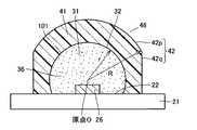
図1は、この発明の実施の形態1における発光装置を示す断面図である。図2は、図1中の発光装置を示す平面図である。図1中には、図2中のI−I線上に沿った断面が示されている。(Embodiment 1)
1 is a cross-sectional view showing a light-emitting device according to
図1および図2を参照して、本実施の形態における発光装置10は、基板21、LED素子26、蛍光体層31および透明樹脂層41を有して構成されている。 With reference to FIG. 1 and FIG. 2, the light-emitting
基板21は、平面状に延在する主表面22を有する。主表面22には、LED素子26が設けられている。図示されていないが、LED素子26は、たとえばダイボンドペーストおよびワイヤーを用いて、基板21に対して物理的および電気的に接続されている。LED素子26は、赤(R)、緑(G)および青(B)のいずれかの色で発光する。一例として、LED素子26は、0.3mm以上の大きさを有する。LED素子26は、その発光色に応じて、GaN、サファイア、GaAsまたはAlGaInPなどから形成されている。 The
内郭部である蛍光体層31は、LED素子26を取り囲むように主表面22上に設けられている。外郭部である透明樹脂層41は、さらに蛍光体層31を覆うように設けられている。蛍光体層31は、主表面22上においてLED素子26と透明樹脂層41との間の空間を完全に充填するように設けられている。透明樹脂層41の周囲には、大気層46が存在する。すなわち、LED素子26の周囲には、内から順に、蛍光体層31、透明樹脂層41および大気層46が配置されている。 The
蛍光体層31および透明樹脂層41は、LED素子26の封止樹脂として設けられている。蛍光体層31および透明樹脂層41は、それぞれ半径rおよび半径Rを有し、原点Oを中心とする同心の半球状に形成されている。原点Oは、主表面22に配置されている。LED素子26は、原点Oに重なる位置に配置されている。 The
このような構成において、透明樹脂層41は、半径Rの外周面42を有する。外周面42は、原点Oを中心とする球面状に形成されている。外周面42は、透明樹脂層41と大気層46との境界をなす表面である。蛍光体層31は、半径rの外周面32を有する。外周面32は、原点Oを中心とする球面状に形成されている。外周面32は、蛍光体層31と透明樹脂層41との境界をなす表面である。 In such a configuration, the
外周面42が半径Rの円弧状となって表れる図1中に示す断面において、蛍光体層31の全体を含み、外周面42と同心となる(原点Oを中心とする)最小の円周101を規定する。円周101は、半径rを有する。本実施の形態では、透明樹脂層41および蛍光体層31が同心の半球状に形成されているため、円周101と外周面32とが重なる。 In the cross section shown in FIG. 1 in which the outer
蛍光体層31は、LED素子26から発せられた光を透過させる樹脂から形成されている。蛍光体層31は、たとえば、透明なエポキシ樹脂またはシリコーン樹脂から形成されている。蛍光体層31には、複数の蛍光粒子36が分散して設けられている。LED素子26から発せられた光は、蛍光粒子36により波長変換され、その結果、LED素子26から発せられた光とは異なる波長の光が、蛍光体層31から発せられる。 The
なお、蛍光粒子36は、例えばBOSE(Ba、O、Sr、Si、Eu)などを好適に用いることができる。またBOSEの他、SOSE(Sr、Ba、Si、O、Eu)、YAG(Ce賦活イットリウム・アルミニウム・ガーネット)、αサイアロン((Ca)、Si、Al、O、N、Eu)、βサイアロン(Si、Al、O、N、Eu)等を好適に用いることができる。また、LED素子26としては発光ピーク波長が450nmの青色発光素子を用いたが、これに代え、例えば発光ピーク波長が390nmから420nmの紫外(近紫外)LED素子とすることにより、さらなる発光効率の向上を図ることができる。 For example, BOSE (Ba, O, Sr, Si, Eu) or the like can be suitably used as the
なお、本実施の形態では、発光装置10が蛍光体層31を有する場合について説明を進めるが、蛍光体層31に替えて、光拡散層が設けられてもよい。光拡散層には、LED素子26から発せられた光を散乱させる、たとえば、TiO2、SiO2、アルミナ、窒化アルミニウム、またはムライトの粉末(粒径は、たとえば10nm〜10μm)などを成分とする散乱粒子が分散して設けられる。また、色むらを抑えるため、蛍光粒子および散乱粒子を混合して用いてもよい。In the present embodiment, the case where the
透明樹脂層41は、LED素子26および蛍光体層31から発せられた光を透過させる樹脂から形成されている。透明樹脂層41は、たとえば、透明なエポキシ樹脂またはシリコーン樹脂から形成されている。透明樹脂層41は、屈折率nを有する。好ましくは、蛍光体層31は、屈折率nよりも大きい屈折率n’を有する。この場合、LED素子26の周囲により大きい屈折率を有する蛍光体層31を配置することにより、LED素子26からの光の取り出し効率を向上させることができる。 The
発光装置10においては、LED素子26から発せられた1次光と、蛍光体層31から発せられた2次光とが混合された光が、透明樹脂層41を透過して、大気層46に取り出される。この際、LED素子26の発光色と蛍光体層31の発光色とを適宜組み合わせることによって、発光装置10から取り出される光の色を自由に選択することができる。 In the
蛍光体層31の形状ならびに透明樹脂層41の材質および形状は、R>r・nの関係が成立するように決定されている。このような構成により、円周101の内側で発せられた光を効率的に大気層46に取り出すことができる。以下、その理由について説明する。 The shape of the
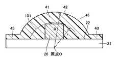
図3は、図1中の発光装置を原点Oを中心とする座標上に模式的に示した図である。図3を参照して、原点Oを中心とする座標上において、円周101上の任意の位置に発光点Lがプロットされ、発光点Lから発せられた光が入射角αで入射する外周面42上の位置に樹脂表面Aがプロットされている。原点Oおよび発光点L間を結ぶ線分と、発光点Lおよび樹脂表面A間を結ぶ線分とがなす角度を、θとする。 FIG. 3 is a diagram schematically showing the light emitting device in FIG. 1 on coordinates with the origin O as the center. Referring to FIG. 3, an outer peripheral surface on which light emission points L are plotted at arbitrary positions on the
このとき、正弦定理より下記の関係式が成立する。
(R/sinθ)=(r/sinα)
上式を整理すると、
sinα=r・sinθ/R
となり、この式から、θ=π/2のとき、αは最大値(αmax)をとる。At this time, the following relational expression is established from the sine theorem.
(R / sin θ) = (r / sin α)
Organizing the above formula,
sin α = r · sin θ / R
From this equation, when θ = π / 2, α takes the maximum value (αmax).
すなわち、下記の(式1)が成立する。
sinα≦sin(αmax)=r/R (式1)
入射角αと、透明樹脂層41および大気層46の境界における全反射の臨界角θcとの間には、スネルの法則から下記の(式2)が成立する。
sinθc=1/n (式2)
今、発光装置10において常にα<θc、すなわち、
αmax<θc (式3)
の関係が成立するならば、発光点Lから発せられた光を全て大気層46に取り出すことができる。That is, the following (Formula 1) is established.
sin α ≦ sin (αmax) = r / R (Formula 1)
The following (Formula 2) is established between the incident angle α and the critical angle θc of total reflection at the boundary between the
sin θc = 1 / n (Formula 2)
Now, in the
αmax <θc (Formula 3)
If this relationship is established, all the light emitted from the light emitting point L can be extracted to the
(式1)〜(式3)を整理すると、下記の関係式が成立する。
r/R=sin(αmax)<sinθc=1/n
結果、R>r・nの関係が成立するように蛍光体層31および透明樹脂層41を設けることによって、円周101の内側から外側に発せられた光を全て大気層46に取り出すことができる。By arranging (Formula 1) to (Formula 3), the following relational expression is established.
r / R = sin (αmax) <sin θc = 1 / n
As a result, by providing the
図4は、透明樹脂層の外周面の半径と光の取り出し効率との関係を示すグラフである。図4を参照して、上述のR>r・nの関係式が、大気層46への光の取り出し効率にどのような影響を与えるかを検証するため、シミュレーションを行なった。本シミュレーションでは、円周101の半径rおよび蛍光体層31の屈折率nを、r=0.9mm,n=1.41(r・n=1.27mm)に固定し、外周面42の半径Rと光の取り出し効率との関係を求めた。光の取り出し効率は、半径R=0.9mmのときの値を100とし、この値を基準に規格化した。 FIG. 4 is a graph showing the relationship between the radius of the outer peripheral surface of the transparent resin layer and the light extraction efficiency. Referring to FIG. 4, a simulation was performed in order to verify how the above relational expression of R> r · n affects the light extraction efficiency to the
グラフから分かるように、外周面42の半径Rが大きくなるほど、光の取り出し効率が増大した。取り出し効率の増え率は、全反射の影響を受けるR≦1.27mmの範囲で、比較的大きく、全反射の影響を受けないR>1.27mmの範囲で比較的小さくなった。また、取り出し効率の値は、114〜115の近辺でほぼ飽和する結果となった。以上の結果より、R>r・nの関係式に従って蛍光体層31の形状ならびに透明樹脂層41の材質および形状を最適化することにより、光の取り出し効率が最大14〜15パーセント程度向上することを確認できた。 As can be seen from the graph, the light extraction efficiency increased as the radius R of the outer
この発明の実施の形態1における発光装置10は、主表面22を有する基板21と、主表面22上に設けられ、光を放つ基点を内包する内郭部としての蛍光体層31と、屈折率nを有し、蛍光体層31を覆う外郭部としての透明樹脂層41とを備える。透明樹脂層41は、大気との境界をなす外周面42を有する。外周面42の少なくとも一部が半径Rの円弧状となって表れる切断面において、蛍光体層31の全てを含み、外周面42と同心となる最小の円周101が半径rを有する場合に、R>r・nの関係が満たされる。 A light-emitting
発光装置10は、蛍光体層31によって取り囲まれ、1次光を発する半導体発光素子としてのLED素子26と、蛍光体層31に分散して設けられ、1次光の一部を吸収して2次光を発し、上記基点に配置される蛍光粒子36とをさらに備える。 The light-emitting
なお、本実施の形態では、内郭部および外郭部として透明な樹脂から形成された蛍光体層31および透明樹脂層41を設けたが、これに限らず、たとえば光を透過するガラスから形成された光透明ガラス層を設けてもよい。 In the present embodiment, the
このように構成された、この発明の実施の形態1における発光装置によれば、透明樹脂層41と大気層46との境界で生じていた全反射と、この全反射に伴う封止樹脂内への光の閉じ込め現象とを解消することができる。すなわち、LED素子26および蛍光体層31から発せられ、透明樹脂層41に進行した光を、透明樹脂層41と大気層46との境界で反射させることなく、大気層46に取り出すことができる。これにより、光の取り出し効率を向上させることができる。 According to the light emitting device according to the first embodiment of the present invention configured as described above, total reflection occurring at the boundary between the
(実施の形態2)
本実施の形態では、実施の形態1において説明した図1中の発光装置10の各種変形例について説明を行なう。以下、重複する構造については説明を繰り返さず、発光装置10と比較した場合に異なる構造を中心に説明を行なう。(Embodiment 2)
In the present embodiment, various modifications of the
図5は、図1中の発光装置の第1変形例を示す断面図である。図5を参照して、本変形例では、内郭部である蛍光体層31が直方体形状の角型を有する。蛍光体層31の全体を含む最小の円周101が半径rを有する場合に、R>r・nの関係が成立する。本変形例に示すように、蛍光体層31の形状は、球状に限られず、直方体、多角柱、円柱などの任意の形状を取り得る。 FIG. 5 is a cross-sectional view showing a first modification of the light emitting device in FIG. Referring to FIG. 5, in the present modification,
図6は、図1中の発光装置の第2変形例を示す断面図である。図6を参照して、本変形例では、内郭部である蛍光体層31が、主表面22上において、LED素子26と蛍光体層31との間に中空層51を形成するように設けられている。すなわち、LED素子26の周囲には、内から順に、中空層51、蛍光体層31、透明樹脂層41および大気層46が配置されている。なお、中空層51に替えて、透明樹脂層41を形成する透明の樹脂が配置されてもよい。 FIG. 6 is a cross-sectional view showing a second modification of the light emitting device in FIG. Referring to FIG. 6, in this modification,
図7は、図1中の発光装置の第3変形例を示す断面図である。図7を参照して、本変形例では、内郭部である蛍光体層31が、内側蛍光体層31mおよび外側蛍光体層31nを含んで構成されている。LED素子26の周囲には、内から順に、内側蛍光体層31m、外側蛍光体層31n、透明樹脂層41および大気層46が配置されている。内側蛍光体層31mと外側蛍光体層31nとの間では、各蛍光体層に分散される蛍光粒子36の種類が異なる。一例を挙げれば、内側蛍光体層31mに分散される蛍光粒子36は赤色で発光し、外側蛍光体層31nに分散される蛍光粒子36は緑色で発光する。 FIG. 7 is a cross-sectional view showing a third modification of the light emitting device in FIG. Referring to FIG. 7, in the present modification,
図8は、図1中の発光装置の第4変形例を示す断面図である。図8を参照して、本変形例では、外周面42および円周101の中心となる原点Oが、主表面22からずれた位置に配置されている。原点Oは、主表面22に対して蛍光体層31および透明樹脂層41の反対側にずれている。このような構成においては、蛍光体層31および透明樹脂層41が完全な半球形状を有しない。 FIG. 8 is a cross-sectional view showing a fourth modification of the light emitting device in FIG. Referring to FIG. 8, in the present modification, the origin O that is the center of the outer
図9は、図1中の発光装置の第5変形例を示す断面図である。図9を参照して、本変形例では、外周面42および円周101の中心となる原点Oが、主表面22からずれた位置に配置されている。原点Oは、主表面22に対して基板21の反対側にずれている。透明樹脂層41は、主表面22に交差する周縁部分が欠けた形状を有する。たとえば、発光装置を導光板の側面に配置するエッジライト方式の液晶バックライトを想定し、透明樹脂層41のサイズを導光板の厚みよりも小さくする必要がある場合に、導光板に対してはみ出る透明樹脂層41の一部をカットしてもよい。すなわち、図9中に示す断面において、外周面42は、半径Rの円弧状となって表れる円弧部42pと、円弧部42pから直線状に延びて主表面22に交わる直線部42qとを含んで構成される。本変形例に示すように、外周面42は、完全な球面状に形成されなくてもよい。 FIG. 9 is a cross-sectional view showing a fifth modification of the light emitting device in FIG. Referring to FIG. 9, in the present modification, the origin O that is the center of the outer
なお、光の取り出し効率の低下を防ぐため、好ましくは、直線部42qの高さは可能な限り低く抑えられる。 In order to prevent a decrease in light extraction efficiency, the height of the straight portion 42q is preferably kept as low as possible.
以上に説明した変形例においても、R>r・nの関係を満たすように蛍光体層31および透明樹脂層41を設けることによって、大気層46への光の取り出し効率を向上させることができる。 Also in the modification described above, the light extraction efficiency to the
図10は、図1中の発光装置の第6変形例を示す断面図である。本変形例では、主表面22上に蛍光体層31が設けられておらず、LED素子26が透明樹脂層41により直接覆われている。LED素子26の全体を含む最小の円周101が半径rを有する場合に、R>r・nの関係が成立する。すなわち、本変形例における発光装置は、主表面22を有する基板21と、主表面22上に設けられ、光を放つ基点を内包する内郭部としてのLED素子26と、屈折率nを有し、LED素子26を覆う外郭部としての透明樹脂層41とを備える。 FIG. 10 is a cross-sectional view showing a sixth modification of the light emitting device in FIG. In this modification, the
透明樹脂層41は、突条部43を含んで形成されている。突条部43は、外周面42から突出し、主表面22上で線状に延びている。突条部43は、金型を用いて透明樹脂層41をインジェクション成型する際に、樹脂の注入経路によって生じた部分である。 The
本変形例においても、R>r・nの関係を満たすようにLED素子26および透明樹脂層41を設けることによって、大気層46への光の取り出し効率を向上させることができる。 Also in this modification, the light extraction efficiency to the
このように構成された、この発明の実施の形態2における発光装置によれば、実施の形態1に記載の効果を同様に得ることができる。 According to the light emitting device according to the second embodiment of the present invention configured as described above, the effects described in the first embodiment can be obtained similarly.
(実施の形態3)
本実施の形態では、図1中の発光装置10の構造を利用した発光装置と、この発光装置を用いた面照明装置および液晶表示装置とについて説明を行なう。以下、重複する構造については説明を繰り返さず、発光装置10と比較した場合に異なる構造を中心に説明を行なう。(Embodiment 3)
In this embodiment, a light-emitting device using the structure of the light-emitting
図11Aおよび図11Bは、この発明の実施の形態3における発光装置を示す図である。図11Bは平面図であり、図11Aは、図11B中のA−A線上に沿った断面図である。 11A and 11B are diagrams showing a light-emitting device according to Embodiment 3 of the present invention. 11B is a plan view, and FIG. 11A is a cross-sectional view taken along the line AA in FIG. 11B.
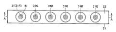
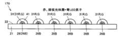
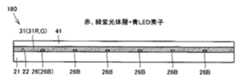
図11Aおよび図11Bを参照して、本実施の形態における発光装置110においては、主表面22上に、複数のLED素子26が互いに間隔を隔てて直線状に並んで配置されている。LED素子26の各々は、図1中の発光装置10と同様の形態で、蛍光体層31および透明樹脂層41により覆われている。このような構成により、発光装置110は、線光源を構成している。 Referring to FIGS. 11A and 11B, in light emitting
本実施の形態では、(青色で発光する青LED素子26B+赤色で発光する赤蛍光体層31R)の組み合わせと、(青色で発光する青LED素子26B+緑色で発光する緑蛍光体層31G)の組み合わせとが、交互に配置されている。 In the present embodiment, a combination of (
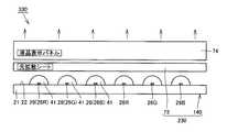
図12は、図11Aおよび図11B中の発光装置を用いた面照明装置および液晶表示装置を示す断面図である。図12を参照して、面照明装置210は、液晶表示装置310のバックライトとして利用されるエッジライト方式の面光源である。 FIG. 12 is a cross-sectional view showing a surface illumination device and a liquid crystal display device using the light emitting device in FIGS. 11A and 11B. Referring to FIG. 12, the
面照明装置210は、発光装置110、導光板61、反射板72および光拡散シート73を有して構成されている。導光板61は、平面状に延在する出射面63と、出射面63の周縁に配置され、導光板61の厚み方向に延在する入射端面62とを有する。導光板61は、入射端面62と基板21の主表面22とが向い合うように、発光装置110に対して位置決めされている。光拡散シート73は、出射面63に重なるように配置されている。反射板72は、導光板61に対して光拡散シート73の反対側に配置されている。 The
液晶表示装置310は、面照明装置210に加えて、液晶表示パネル74を有して構成されている。液晶表示パネル74は、光拡散シート73に対して導光板61の反対側に配置されている。すなわち、出射面63上には、光拡散シート73および液晶表示パネル74が順に配置されている。液晶表示パネル74の表示面の側を正面とすれば、面照明装置210は、液晶表示パネル74の背面に配置されている。 The liquid
発光装置110から発せられた光は、入射端面62を通じて導光板61内に入射される。この際、透明樹脂層41の直径2Rを導光板61の厚みTよりも小さく設定することにより(R<T/2)、発光装置110から発せられた光を効率良く導光板61内に入射させることができる。導光板61内に入射した光は、反射板72によって反射されながら、出射面63を通じて液晶表示パネル74に向けて出射される。 The light emitted from the
続いて、図11Aおよび図11B中の発光装置の各種変形例と、その発光装置を用いた面照明装置および液晶表示装置とについて説明を行なう。 Next, various modifications of the light emitting device in FIGS. 11A and 11B, and a surface illumination device and a liquid crystal display device using the light emitting device will be described.
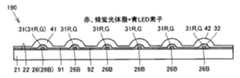
図13Aおよび図13Bは、図11Aおよび図11B中の発光装置の第1変形例を示す図である。図13Bは平面図であり、図13Aは、図13B中の矢印Aに示す方向から見た側面図である。 13A and 13B are diagrams showing a first modification of the light emitting device in FIGS. 11A and 11B. FIG. 13B is a plan view, and FIG. 13A is a side view seen from the direction indicated by arrow A in FIG. 13B.
図13Aおよび図13Bを参照して、本変形例における発光装置120においては、主表面22上に、複数のLED素子26が互いに間隔を隔てて直線状に並んで配置されている。主表面22上には隔壁81が立設されており、直線状に並ぶ複数のLED素子26が、隔壁81を隔てた両側にそれぞれ設けられている。LED素子26の各々は、図1中の発光装置10と同様の形態で、蛍光体層31および透明樹脂層41により覆われている。 With reference to FIG. 13A and FIG. 13B, in the light-emitting
本変形例では、隔壁81を隔てた両側の一方の側に、(青色で発光する青LED素子26B+緑色で発光する緑蛍光体層31G)の組み合わせが配置され、隔壁81を隔てた両側の他方の側に、(青色で発光する青LED素子26B+赤色で発光する赤蛍光体層31R)の組み合わせが配置されている。 In this modification, a combination of (
図14は、図13Aおよび図13B中の発光装置を用いた面照明装置および液晶表示装置を示す断面図である。図14を参照して、図13Aおよび図13B中に示す発光装置120を用いた面照明装置220および液晶表示装置320は、図12中の面照明装置210および液晶表示装置310と同様の構造を有する。面照明装置220および液晶表示装置320においては、隔壁81を隔てた両側の一方の側から発せられた緑色光が、隔壁81を隔てた両側の他方の側に配置された(青色で発光する青LED素子26B+赤色で発光する赤蛍光体層31R)の組み合わせからなる発光装置に吸収されることを抑制できる。 FIG. 14 is a cross-sectional view showing a surface illumination device and a liquid crystal display device using the light emitting device in FIGS. 13A and 13B. Referring to FIG. 14,
図15Aおよび図15Bは、図11Aおよび図11B中の発光装置の第2変形例を示す図である。図15Bは平面図であり、図15Aは、図15B中のA−A線上に沿った断面図である。 15A and 15B are diagrams showing a second modification of the light emitting device in FIGS. 11A and 11B. 15B is a plan view, and FIG. 15A is a cross-sectional view taken along the line AA in FIG. 15B.
図15Aおよび図15Bを参照して、本変形例における発光装置130においては、主表面22上に、複数のLED素子26が互いに間隔を隔てて直線状に並んで配置されている。本変形例では、透明樹脂層41により直接覆われ、赤色で発光する赤LED素子26Rと、図1中の発光装置10と同様の形態で、緑色で発光する緑蛍光体層31Gおよび透明樹脂層41により覆われ、青色で発光する青LED素子26Bとが交互に配置されている。 With reference to FIG. 15A and FIG. 15B, in the light-emitting
なお、図13Aおよび図13B中に示す(青色で発光する青LED素子26B+赤色で発光する赤蛍光体層31R)の組み合わせを、透明樹脂層41により直接覆われる赤LED素子26Rに置き換える構成としてもよい。 13A and 13B may be replaced with a
本変形例における発光装置130を用いた面照明装置および液晶表示装置は、図12中の面照明装置210および液晶表示装置310と同様の構造を有して構成される。 The surface illumination device and the liquid crystal display device using the
このように構成された、この発明の実施の形態3における発光装置、面照明装置および液晶表示装置によれば、実施の形態1に記載の効果を同様に得ることができる。加えて、光の取り出し効率に優れた発光装置の使用により、高輝度を有する面照明装置60を実現し、さらに液晶表示パネル74における表示の明るさを向上させることができる。 According to the light emitting device, the surface illumination device, and the liquid crystal display device according to the third embodiment of the present invention configured as described above, the effects described in the first embodiment can be similarly obtained. In addition, by using a light emitting device having excellent light extraction efficiency, the surface illumination device 60 having high luminance can be realized, and the brightness of display on the liquid
なお、本実施の形態では、蛍光体層31および透明樹脂層41が図1中の発光装置10と同様の形態で設けられる場合を説明したが、蛍光体層31および透明樹脂層41は、実施の形態2における各種変形例と同様の形態で設けられてもよい。 In the present embodiment, the case where the
(実施の形態4)
本実施の形態では、図10中の発光装置の構造を利用した発光装置と、この発光装置を用いた面照明装置および液晶表示装置とについて説明を行なう。以下、重複する構造については説明を繰り返さず、図10中の発光装置と比較した場合に異なる構造を中心に説明を行なう。(Embodiment 4)
In this embodiment mode, a light-emitting device using the structure of the light-emitting device in FIG. 10, and a surface illumination device and a liquid crystal display device using the light-emitting device will be described. Hereinafter, the description of the overlapping structure will not be repeated, and the description will be focused on a different structure when compared with the light emitting device in FIG.
図16は、この発明の実施の形態4における発光装置を示す平面図である。図17は、図16中の発光装置を用いた面照明装置および液晶表示装置を示す断面図である。 FIG. 16 is a plan view showing a light-emitting device according to Embodiment 4 of the present invention. 17 is a cross-sectional view showing a surface illumination device and a liquid crystal display device using the light emitting device in FIG.
図16を参照して、本実施の形態における発光装置140においては、複数のLED素子26が、互いに間隔を隔てて平面状に並んで配列されている。複数のLED素子26の各々は、図10中に示す発光装置と同様の形態で、透明樹脂層41により覆われている。本実施の形態では、赤色で発光する赤LED素子26Rと、緑色で発光する緑LED素子26Gと、青色で発光する青LED素子26Bとが、順に並んで配置されている。このような構成により、発光装置140は、面光源を構成している。 Referring to FIG. 16, in light emitting
図17を参照して、本実施の形態における面照明装置230は、液晶表示装置330のバックライトとして利用される直下型方式の面光源である。面照明装置230は、発光装置140および光拡散シート73を有して構成されている。光拡散シート73は、基板21の主表面22に向い合うように、発光装置140に対して位置決めされている。 Referring to FIG. 17,
液晶表示装置330は、面照明装置230に加えて、液晶表示パネル74を有して構成されている。液晶表示パネル74は、光拡散シート73に対して発光装置140の反対側に配置されている。 The liquid
このように構成された、この発明の実施の形態4における発光装置、面照明装置および液晶表示装置によれば、実施の形態3に記載の効果を同様に得ることができる。 According to the light emitting device, the surface illumination device, and the liquid crystal display device according to the fourth embodiment of the present invention configured as described above, the effects described in the third embodiment can be similarly obtained.
(実施の形態5)
本実施の形態では、図1中の発光装置10の別の形態について説明を行なう。以下、重複する構造については説明を繰り返さない。(Embodiment 5)
In the present embodiment, another embodiment of the
図18は、この発明の実施の形態5における発光装置を示す斜視図である。図18を参照して、本実施の形態における発光装置10’では、蛍光体層31および透明樹脂層41が、半円形の断面をその中心軸106の軸方向に伸長させた半円柱形状を有する。中心軸106に直交する平面で発光装置10’を切断した場合に図1中に示す形状と同様の切断面が得られ、この切断面において、蛍光体層31および透明樹脂層41は、R>r・nの関係が成立するように設けられている。このように、蛍光体層31および透明樹脂層41は、球形状に限られず、図1中に示す断面形状を含む任意の形状を取り得る。 FIG. 18 is a perspective view showing a light-emitting device according to Embodiment 5 of the present invention. Referring to FIG. 18, in light emitting
図19Aおよび図19Bは、図18中の発光装置の構造を利用した発光装置を示す図である。図19Bは平面図であり、図19Aは、図19B中のA−A線上に沿った断面図である。 19A and 19B are diagrams showing a light emitting device using the structure of the light emitting device in FIG. 19B is a plan view, and FIG. 19A is a cross-sectional view taken along line AA in FIG. 19B.
図19Aおよび図19Bを参照して、発光装置170においては、主表面22上に、青で発光する複数の青LED素子26Bが互いに間隔を隔てて直線状に並んで配置されている。青LED素子26Bの各々は、赤および緑で発光する赤,緑蛍光体層31R,Gと、透明樹脂層41とにより覆われている。中心軸106の軸方向と複数のLED素子26の配列方向とが、直交する。 Referring to FIGS. 19A and 19B, in light emitting
なお、本実施の形態では、複数のLED素子26を単一の基板21に実装した例を説明したが、本発明はこのような形態に限られず、後述の実施の形態10に説明するように、LED素子26は、それぞれ各基板21に搭載された形態で個別の発光装置を構成し、この発光装置を筐体基板や実装基板などに搭載する構造としてもよい。 In the present embodiment, an example in which a plurality of
図20Aおよび図20Bは、図19Aおよび図19B中の発光装置の変形例を示す図である。図20Bは平面図であり、図20Aは、図20B中のA−A線上に沿った断面図である。 20A and 20B are diagrams showing a modification of the light emitting device in FIGS. 19A and 19B. 20B is a plan view, and FIG. 20A is a cross-sectional view taken along the line AA in FIG. 20B.
図20Aおよび図20Bを参照して、本変形例における発光装置180においては、主表面22上に、青で発光する複数の青LED素子26Bが互いに間隔を隔てて直線状に並んで配置されている。複数の青LED素子26Bは、共通の赤,緑蛍光体層31R,Gおよび透明樹脂層41により覆われている。複数の青LED素子26Bの配列方向に対して直角の方向における発光装置180の断面は、実施の形態2における変形例3(図7)に示す断面と同一形状であり、赤,緑蛍光体層31R,Gおよび透明樹脂層41の寸法関係も、実施の形態2における変形例3(図7)の関係と同一である。本変形例では、中心軸106の軸方向と複数のLED素子26の配列方向とが一致する。 Referring to FIGS. 20A and 20B, in light emitting
本変形例における発光装置180を用いた面照明装置および液晶表示装置は、図12中の面照明装置210および液晶表示装置310と同様の構造を有して構成される。 The surface illumination device and the liquid crystal display device using the
このように構成された、この発明の実施の形態5における発光装置によれば、実施の形態1に記載の効果を同様に得ることができる。 According to the light emitting device in the fifth embodiment of the present invention configured as described above, the effects described in the first embodiment can be obtained similarly.
(実施の形態6)
本実施の形態では、図1中の発光装置10の構造を利用した発光装置について説明を行なう。以下、重複する構造については説明を繰り返さず、図1中の発光装置10と比較した場合に異なる構造を中心に説明を行なう。(Embodiment 6)
In this embodiment, a light-emitting device using the structure of the light-emitting
図21Aおよび図21Bは、この発明の実施の形態6における発光装置を示す図である。図21Bは平面図であり、図21Aは、図21B中のA−A線上に沿った断面図である。 21A and 21B are diagrams showing a light emitting device according to Embodiment 6 of the present invention. 21B is a plan view, and FIG. 21A is a cross-sectional view taken along the line AA in FIG. 21B.
図21Aおよび図21Bを参照して、本実施の形態における発光装置190においては、主表面22上に、青で発光する複数の青LED素子26Bが互いに間隔を隔てて直線状に並んで配置されている。青LED素子26Bの各々は、赤および緑で発光する赤,緑蛍光体層31R,Gと、透明樹脂層41とにより覆われている。 Referring to FIGS. 21A and 21B, in light-emitting
透明樹脂層41および蛍光体層31は、それぞれ、突条部91および突条部92を含んで形成されている。突条部92は、外周面32から突出し、主表面22上で線状に延びている。突条部91は、外周面42から突出し、主表面22上で突条部92を覆うように線状に延びている。突条部91は、隣接する透明樹脂層41間で延び、突条部92は、隣接する蛍光体層31間で延びている。突条部91および突条部92は、金型を用いて透明樹脂層41および蛍光体層31をインジェクション成型する際に、樹脂の注入経路によって生じた部分である。 The
図22Aおよび図22Bは、図21Aおよび図21B中の発光装置の変形例を示す図である。図22Bは平面図であり、図22Aは、図22B中のA−A線上に沿った断面図である。 22A and 22B are diagrams showing a modification of the light emitting device in FIGS. 21A and 21B. 22B is a plan view, and FIG. 22A is a cross-sectional view taken along the line AA in FIG. 22B.
図22Aおよび図22Bを参照して、本変形例における発光装置200においては、透明樹脂層41が突条部91を含んで形成されている。一方、複数の蛍光体層31は、互いに独立して主表面22上に設けられている。蛍光体層31は、図1中の円周101に収まる形状であれば自由な形状を取り得るため、透明樹脂層41と比較して形状の精度に対する要求が低い。このため、蛍光体層31は、複数のLED素子26間の配向特性や輝度、色度が所定のばらつき範囲内にあれば、ディスペンサーを用いた塗布などの方法により形成されてもよい。 With reference to FIG. 22A and FIG. 22B, in the
このように構成された、この発明の実施の形態6における発光装置によれば、実施の形態1に記載の効果を同様に得ることができる。 According to the light emitting device in the sixth embodiment of the present invention configured as described above, the effects described in the first embodiment can be obtained similarly.
以上の実施の形態1から6に説明した発光装置、面照明装置および液晶表示装置の構造を適宜組み合わせて、新たな発光装置、面照明装置および液晶表示装置を構成してもよい。 A new light emitting device, surface lighting device, and liquid crystal display device may be configured by appropriately combining the structures of the light emitting device, the surface lighting device, and the liquid crystal display device described in the first to sixth embodiments.
(実施の形態7)
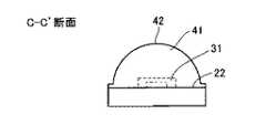
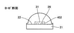
図23A、図23Bおよび図23Cは、この発明の実施の形態7における発光装置を示す図である。図23Aは平面図であり、図23Bは、図23A中のB−B´線上に沿った断面図であり、図23Cは、図23A中のC−C´線上に沿った断面図である。(Embodiment 7)
FIG. 23A, FIG. 23B, and FIG. 23C are diagrams showing a light-emitting device according to Embodiment 7 of the present invention. 23A is a plan view, FIG. 23B is a cross-sectional view taken along the line BB ′ in FIG. 23A, and FIG. 23C is a cross-sectional view taken along the line CC ′ in FIG. 23A.
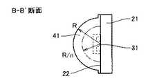
図23A、図23Bおよび図23Cを参照して、本実施の形態における発光装置510は、基板21と、基板21の主表面22の中央部にダイボンディングされた4個のLED素子26と、これらのLED素子26を被覆する蛍光体層31と、蛍光体層31を半球ドーム状の形状にて被覆する透明樹脂層41とを備える。透明樹脂層41は、屈折率n=1.41を有する。透明樹脂層41は、主表面22を半径R(1.4mm)の円により被覆する。一方、蛍光体層31は、半径Rの円と同心の半径R/nの半球内(図中に、一点鎖線の仮想線で示す)に形成される。 Referring to FIGS. 23A, 23B, and 23C, light-emitting
このように、発光装置510は、主表面22において、LED素子26の近傍のみが蛍光体層31により被覆され、LED素子26より遠い部分は蛍光体層31により被覆されないところに特徴を有する。 As described above, the
蛍光体層31は、LED素子26が発する1次光により励起され、2次光を発する。これに対して、2次光の出射は、LED素子26近傍の蛍光体層31による成分が主であって、LED素子26より遠い部分による成分は小さい。蛍光体層31がLED素子26より遠い部分において主表面22を被覆する場合、主表面22での反射作用を阻害するとともに、出射光の一部を吸収する作用を呈し、光の取り出し効率を低下させることがある。このため、蛍光体層31は主表面22においてLED素子26の近傍のみ被覆し、遠い部分は被覆しない構成とすることが好ましい。これにより、主表面22が備える反射作用を有効に利用し、光の取り出し効率を向上させることができる。 The
以下、発光装置の製造方法について説明する。図24Aは、この発明の実施の形態7における発光装置の製造方法の工程を示す断面図である。図24Bは、この発明の実施の形態7における発光装置の製造方法の変形例の工程を示す断面図である。 Hereinafter, a method for manufacturing the light emitting device will be described. FIG. 24A is a cross-sectional view showing a step in the manufacturing method for the light emitting device according to Embodiment 7 of the present invention. FIG. 24B is a cross-sectional view showing a process of a modification of the method for manufacturing the light-emitting device in Embodiment 7 of the present invention.
なお、図中に示す構成要素は、不明瞭とならない程度に必要に応じて簡略化されて示されている。 In addition, the component shown in the figure is simplified as needed to such an extent that it may not become obscure.
図24Aを参照して、まず、基板21の主表面22の所定の位置に、LED素子26をダイボンディングする。次に、LED素子26の電極と基板21の電極(図示しない)とを、ワイヤー27によりワイヤボンディングし、電気的に接続する。主表面22にワイヤボンディング用の電極、基板21の裏面に外部の回路と接続するための電極が設けられ、両者は、スルーホールにより導通されている(図示しない)。このような構成により、発光装置は、LED素子26に電力を供給可能に構成されている。基板21の材質は、前述したように主表面22の反射作用が高いことが好ましい。好適には、基材21として、セラミック基板が用いられる。 Referring to FIG. 24A, first,
次に、LED素子26を蛍光体層31で被覆する。まず、主表面22のLED素子26がダイボンディングされた側の面に、堰き止め部材としてのダムシート401を張り付ける。ダムシート401には、LED素子26を収容可能な貫通孔が形成されている。ダムシート401は、LED素子26がその貫通孔に没入するように基板21に張り付けられる部材であり、後述する蛍光粒子入りの樹脂33を貫通孔に注入する時に、樹脂33が主表面22に流出して拡がらないように堰き止める部材である。次に、蛍光粒子入りの樹脂33を、貫通孔を満たすように注入する。このとき、樹脂33は、ダムシート401との間に生じる表面張力により、貫通孔の外への流出が抑制されるとともに、メニスカスを生じることがある。この場合であっても、R>r・nの関係が満たされることが好ましい。 Next, the
蛍光粒子入りの樹脂33は、シリコーン樹脂などの透明樹脂に蛍光粒子36を分散させたものである。ダムシート401としては、たとえば、テフロン(登録商標)やフッ素ゴムなどの樹脂製シートの一方の面に粘着材が塗布されたものを用いることができる。フッ素ゴムは、弾力性が高く、ダムシート401の除去が容易であるため、ダムシート401に使用される材料として好ましい。粘着材は、主表面22への張り付けが容易であるとともに、ダムシート401を除去した際に主表面22に粘着材の残渣が残らないものが好ましい。 The
次に、150℃、120分の条件で、蛍光粒子入りの樹脂33を硬化させた後、ダムシート401を除去することにより、蛍光体層31を形成する。ダムシート401の除去として、ダムシート401の一端を治具により把持し、引き剥す方法が挙げられる。このとき、貫通孔よりはみ出した蛍光粒子入りの樹脂33を、ダムシート401と同時に除去することができる。 Next, after the
次に、蛍光体層31を、透明樹脂により半球ドーム状に被覆する。その方法として、たとえば圧縮成形を用いることができる。圧縮成形による場合、半球ドーム状のキャビティ78cを備える雌型78aを用い、蛍光体層31を半球ドーム状の形状を備えた透明樹脂層41により被覆する。 Next, the
まず、キャビティ78cに透明樹脂40を注入し、満たす。次に、基板21を雌型78aにセットし、ベース型78bにより型締めするとともに、150℃の温度で1分程度保持することによって、透明樹脂40を硬化する。このとき、キャビティ78cに蛍光体層31が没入した状態が得られる。次に、基板21を雌型78aから外す。圧縮成形により半球ドーム状の透明樹脂層41を形成した場合、隣り合うキャビティ間を透明樹脂40が連通することにより、半球ドームの周縁部に薄い透明樹脂層41が延在し、主表面22を被覆することがある。 First, the
次に、150℃、2時間の条件で、アフターキュアを行ない、そのあと、基板21を個別の発光装置に分割する。この際、基板21の裏面に設けられた分割溝の上方を、透明樹脂層41の形成された側から、カッタ79により剪断する方法を採ることができる。このような方法によると、透明樹脂層41がカッタ79により剪断されるとともに、基板21が分割溝に沿って割れることにより、個別の発光装置に容易に分割することができる。 Next, after-cure is performed at 150 ° C. for 2 hours, and then the
続いて、本実施の形態における発光装置510を評価するために実施した実施例について説明する。 Next, examples implemented for evaluating the
前述の製造方法により、図23A、図23Bおよび図23C中に示すように、3.2mm角の基板21上に、半径がR=1.4mmの半球ドーム状の透明樹脂層41を備えた発光装置510を形成した。主表面22の中央部には、4つのLED素子26がダイボンディングされている。4つのLED素子26は、ワイヤボンディングにより直列接続され、さらに蛍光体層31によって被覆されている。半球ドームの中心は、LED素子26の配列の中心かつ主表面22より100μmの高さに配置されている。半球ドームの底面は、直径2.8mmを有し、主表面22から半球ドーム最頂部までの高さは、1.5mmである。半球ドームの周辺部には、厚み50μm程度を有する透明樹脂層41が延在しており、透明樹脂層41は、主表面22を全体的に被覆している。 As shown in FIGS. 23A, 23B, and 23C, the above-described manufacturing method provides light emission including a hemispherical dome-shaped
LED素子26は、寸法240μm×600μm、厚み100μmを有する。4つのLED素子26は、主表面22の中央部の領域内において、主表面22を平面的に見て、2行2列に略等間隔に位置決めされている。 The
蛍光体層31は、寸法0.9mm×1.6mm、厚み0.38mmを有する。蛍光体層31による主表面22の被覆面積は、ほぼ1.4mm2である。一方、半球ドームの底面は、直径2.8mmを有するため、その底面積は6.2mm2である。したがって、蛍光体層31による主表面22の被覆面積の、半球ドームの底面積に対する割合は、23%程度となるが、蛍光体層31の四隅を面取りすることによって、被覆面積のさらなる縮小が図られている。The
上述の説明によると、発光装置510は、主表面22が備える反射作用を有効に利用することを意図するため、蛍光体層31による主表面22の被覆面積の、半球ドームの底面積に対する割合は、特定の値に限定されるべきではない。 According to the above description, since the
実施の形態1において説明した図4中のグラフによると、蛍光体層31の半径rと透明樹脂層41の半径Rとが等しい時、すなわち、蛍光体層31による主表面22の被覆面積の、半球ドームの底面積に対する割合が100%である時の値を基準とすると、光の取り出し効率は、半球ドームの外周面42の半径Rの増加につれて増大し、R>r・nの条件で、概ね飽和する。したがって、光の取り出し効率向上の効果は、蛍光体層31による主表面22の被覆面積の、半球ドームの底面積に対する割合が100%未満、たとえば95%、好ましくは80%以下であっても奏され、(1/n)2付近で飽和する傾向と考えられる。According to the graph in FIG. 4 described in the first embodiment, when the radius r of the
次に、蛍光体層31を圧縮成形により形成した発光装置と、本実施の形態における発光装置510との全光束を比較した。蛍光体層31を圧縮成形により形成した発光装置の場合、その製造方法に起因して、LED素子26がダイボンディングされた位置から延在する蛍光体層により、厚さ100から200μm程度で主表面の一部または全部が被覆されているが、それ以外の構成については、発光装置510と同等である。 Next, the total luminous flux of the light emitting device in which the
その結果、本実施の形態における発光装置510は、蛍光体層31を圧縮成形により形成した発光装置と比較して、10から20%の割合で全光束の増大が確認された。 As a result, in the
このように、主表面22においてLED素子26の近傍のみが蛍光体層31により被覆され、LED素子26より遠い部分は蛍光体層31で被覆されないように構成された発光装置によると、主表面22での反射作用を有効に利用することにより、光の取り出し効率を向上させることができる。また、蛍光体層31の寸法は、貫通孔の寸法により画定されるため、寸法の精度が高く、輝度や色度のばらつきを抑制する上で有利である。 As described above, according to the light emitting device configured such that only the vicinity of the
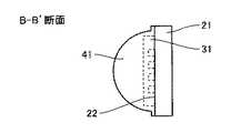
続いて、発光装置510の変形例について説明する。図25A、図25Bおよび図25Cは、図23A、図23Bおよび図23C中の発光装置の変形例を示す図である。図25Aは平面図であり、図25Bは、図25A中のB−B´線上に沿った断面図であり、図25Cは、図25A中のC−C´線上に沿った断面図である。 Subsequently, a modification of the
図25A、図25Bおよび図25Cを参照して、本変形例における発光装置520においては、主表面22の中央部に4つのLED素子26が配置されている。4つのLED素子26は、各LED素子の長手方向が互いに向い合うように一列に、略等間隔にダイボンディングされている。発光装置520は、上記以外の構成については、発光装置510と同等の構成を備える。このような構成によれば、LED素子26とワイヤー27の配列とが一方向であって、ダイボンディングやワイヤボンディングが容易である。 Referring to FIGS. 25A, 25B, and 25C, in light emitting
蛍光体層31は、その長手方向の端部において、半径Rの円と同心の半径R/nの半球(図中に、一点鎖線の仮想線で示す)よりはみ出す。しかしながら、LED素子26は、R>r・nの条件を満たす半径R/nの内部の位置にダイボンディングされるとともに、発光に寄与する蛍光体層31は、主にLED素子26の近傍に配置される部分である。このため、発光点の半球ドーム中心からの位置rは、実質的にR>r・nの条件を満たすものと見なすことができ、光の取り出し効率の向上効果が得られるものと考えられる。したがって、蛍光体層31の一部分の半球ドーム中心からの位置rが、R>r・nの条件を満たさない場合であっても、さらに半球ドームよりはみ出す場合であっても、LED素子26の少なくとも幾つかがR>r・nの条件を満たす位置rにダイボンディングされていれば、光の取り出し効率の向上作用が得られるものと考えられる。 The
なお、蛍光体層31の形成方法の変形例として、図24B中に示すように、蛍光粒子入りの樹脂33を、主表面22にダイボンディングされたLED素子26にポッティングして被覆し、チクソ性により蛍光体層31の形状を維持しつつ硬化させる方法がある。この方法によると、蛍光体層31が幾らか主表面22に拡がるものの、ダムシート401が不要であるため、製造工程が簡便である。 As a modification of the method of forming the
この方法によると、ポッティングは数回に分割して行なうことができる。すなわち、ポッティングと仮硬化とを繰返し、被覆を積層することにより蛍光体層31を形成する。この方法によると、蛍光体層31の寸法の増減が容易である。 According to this method, potting can be performed in several steps. That is, the
(実施の形態8)
本実施の形態における発光装置は、ダムシートが蛍光粒子入りの樹脂を堰き止める作用と、ダムシート自体の反射作用とを兼ね備えるものであって、反射率の高いダムシートを用いるとともに、ダムシートを基板に張り付けたままダムシートの上方にドームが形成されることを特徴とする。それ以外の点は、実施の形態7に説明した発光装置と同等であるので、異なる点について説明する。(Embodiment 8)
The light emitting device in the present embodiment combines the action of the dam sheet blocking the resin containing fluorescent particles and the reflection action of the dam sheet itself. A dome is formed above the dam sheet while being attached to the substrate. Since the other points are the same as those of the light-emitting device described in Embodiment 7, different points will be described.
図26は、この発明の実施の形態8における発光装置の製造方法の工程を示す断面図である。図26を参照して、以下、本実施の形態における発光装置530の製造方法について説明する。まず、前述と同様の方法により、基板21の主表面22に反射率の高いダムシート401を張り付け、次に、主表面22にダイボンディングされたLED素子26を蛍光体層31により被覆する。この際、蛍光粒子入りの樹脂33を貫通孔を満たすように注入する時に、樹脂33をダムシート401の表面に流出して拡がらないようにすることが肝要である。 FIG. 26 is a cross sectional view showing a step in the method for manufacturing the light emitting device in the eighth embodiment of the present invention. With reference to FIG. 26, a method for manufacturing light emitting
次に、ダムシート401を残したまま、蛍光体層31を透明樹脂層41により半球ドーム状に被覆する。半球ドームの形成方法として、インジェクションモールドを用いることができる。雌型78aには、半球ドーム状に形成されたキャビティ78cと、これに連通するゲート78dとが設けられている。基板21を雌型78aにセッティングし、ベース型78bにより型締めする。そのあと、透明樹脂40をゲート78dよりキャビティ78c内に射出することによって、蛍光体層31を半球ドーム状に被覆する。透明樹脂40の射出後、キャビティ78c内で120℃、3分の条件で透明樹脂40を硬化させ、基板21を雌型78aより取り出す。150℃、2時間の条件でアフターキュアを行ない、そのあと、前述と同様の方法により基板21を個別の発光装置に分離させる。 Next, with the
ダムシート401の材料として、たとえば、ゴアテックス(登録商標)など繊維質のシートの表面に樹脂をコーティングし、さらに一方の面に粘着材を塗布したものを用いることができる。 As a material of the
本実施の形態における発光装置530と、比較のための発光装置との全光束を比較した。発光装置530は、セラミック基板21にダムシート401が張り付けられた構成を備えるのに対して、比較のための発光装置では、ダムシート401が設けられていない。それ以外の構成については、両者とも同等の構成を備える。その結果、発光装置530の場合、比較のための発光装置に比べ、1.8から2.7%の全光束が増大することが確認された。 The total luminous fluxes of the
本実施の形態によると、反射性の高いダムシート401が主表面22に張り付けられた構成を備えることにより、樹脂基板や反射率の低い基板材料を用いることができ、基板材質選択の自由度が高い。また、ダムシート401を除去する工程が不要であり、製造工程が簡便である。 According to the present embodiment, by providing a configuration in which the highly
(実施の形態9)
本実施の形態における発光装置においては、ダムシート401に替え、ダムリングが用いられる。ダムリングは、ダムシートと同じく、蛍光粒子入りの樹脂が基板の主表面に流出して拡がらないように堰き止めるための部材である。本実施の形態における発光装置は、ダムリングを備える以外は、実施の形態7に説明した発光装置と同等であるため、異なる点について説明する。(Embodiment 9)
In the light emitting device in the present embodiment, a dam ring is used instead of the
図27Aおよび図27Bは、この発明の実施の形態9における発光装置を示す図である。図27Aは平面図であり、図27Bは、図27A中のB−B´線上に沿った断面図である。 27A and 27B are diagrams showing a light emitting device according to Embodiment 9 of the present invention. 27A is a plan view, and FIG. 27B is a cross-sectional view taken along the line BB ′ in FIG. 27A.
図27Aおよび図27Bを参照して、以下、本実施の形態における発光装置540の製造方法について説明する。発光装置540においては、前述のダムシート401に替えて、主表面22上にLED素子26の周囲を取り囲むようにダムリング402が張り付けられ、ダムリング402の内側に蛍光体層31が形成されている。なお、ダムリング402の材質を透明樹脂層41と同じとすることにより、屈折率差による照射形状の歪みが抑制されるとともに、ダムリング402と透明樹脂層41との間の膨張係数差を解消できる点で好ましい。 With reference to FIGS. 27A and 27B, a method for manufacturing light-emitting
図28は、図27Aおよび図27B中の発光装置の変形例を示す断面図である。図28を参照して、本変形例における発光装置550においては、ダムリング402の断面が、ダムリング402を主表面22に張り付けた状態でLED素子26の周囲を取り囲んでおり、LED素子26と対向する側の壁面が斜面をなしている。発光装置550は、この斜面402aが反射壁として作用することを特徴とする。これにより、発光装置550の出射光に前方への指向性を与えることができる。なお、ダムリング402の材質として、斜面402aの反射率が高いものを用いることが好ましく、金属あるいは反射膜の形成された樹脂などを用いることができる。 FIG. 28 is a cross-sectional view showing a modification of the light emitting device in FIGS. 27A and 27B. Referring to FIG. 28, in the
(実施の形態10)
本実施の形態では、図25A〜図25C中の発光装置520の構造を利用した発光装置と、この発光装置を用いた面照明装置および液晶表示装置とについて説明を行なう。以下、重複する構造については説明を繰り返さず、図25A〜図25C中の発光装置520と比較した場合に異なる構造を中心に説明を行なう。(Embodiment 10)
In this embodiment, a light-emitting device using the structure of the light-emitting
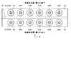
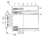
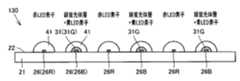
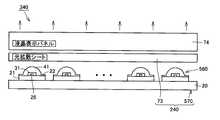
図29は、この発明の実施の形態10における発光装置を示す平面図である。図30は、図29中の発光装置を用いた面照明装置および液晶表示装置を示す断面図である。 FIG. 29 is a plan view showing a light emitting device according to the tenth embodiment of the present invention. 30 is a cross-sectional view showing a surface illumination device and a liquid crystal display device using the light emitting device in FIG.
本実施の形態では、図29および図30を参照して、図25A〜図25C中に示した発光装置520と同じ形態の発光装置560を、筐体基板20上に2次元マトリクス状に複数配列して搭載された面光源570である。発光装置560におけるLED素子26は、青色LED素子とし、蛍光体層31は、黄色蛍光体のみあるいは緑色蛍光体および赤色蛍光体を含む樹脂層として、白色光を放出する発光装置を構成している。 In this embodiment, referring to FIGS. 29 and 30, a plurality of light emitting
なお、LED素子26の搭載数は、4個に限定されず、3個など他の個数であってもよい。また、発光装置560の筐体基板への配列についても、本配列形態に限定されず、たとえば、六角状、三角状などの配列形態でもよい。 Note that the number of
本実施の形態における面照明装置240は、直下型方式のバックライトとして、液晶表示装置340に利用される。面照明装置240は、複数の発光装置560を含む面光源570と、光拡散シート73とを有する。光拡散シート73は、各発光装置560の基板21の主表面22に向い合うように、面光源570に対して位置決めされている。 The
液晶表示装置340は、面照明装置240に加えて、液晶表示パネル74を有して構成されている。液晶表示パネル74は、光拡散シート73に対して面光源570の反対側に配置されている。なお、面照明装置240の輝度、色度むらを改善するために、光拡散シート73に替えて、光学レンズ部材が設置されてもよい。また、光拡散シート73と液晶表示パネル74との間に、集光作用を有する光学シートが挿入されてもよい。 The liquid
このように構成された、この発明の実施の形態10における発光装置、面照明装置および液晶表示装置によれば、実施の形態3に記載の効果を同様に得ることができる。 According to the light emitting device, the surface illumination device, and the liquid crystal display device according to the tenth embodiment of the present invention configured as described above, the effects described in the third embodiment can be similarly obtained.
今回開示された実施の形態はすべての点で例示であって制限的なものではないと考えられるべきである。本発明の範囲は上記した説明ではなくて請求の範囲によって示され、請求の範囲と均等の意味および範囲内でのすべての変更が含まれることが意図される。 The embodiment disclosed this time should be considered as illustrative in all points and not restrictive. The scope of the present invention is defined by the terms of the claims, rather than the description above, and is intended to include any modifications within the scope and meaning equivalent to the terms of the claims.
この発明は、主に、液晶テレビ等の表示装置用バックライトに利用される。 The present invention is mainly used for a backlight for a display device such as a liquid crystal television.
10,10’,110,120,130,140,170,180,190,200,510,520,530,540,550,560 発光装置、21 基板、22 主表面、26 LED素子、31 蛍光体層、31m 内側蛍光体層、31n 外側蛍光体層、33 蛍光粒子入り樹脂、36 蛍光粒子、41 透明樹脂層、42 外周面、46 大気層、61,66 導光板、62 入射端面、63,67 出射面、68 入射面、74 液晶表示パネル、101 円周、210,220,230,240 面照明装置、310,320,330,340 液晶表示装置、401 ダムシート、402 ダムリング。 10, 10 ′, 110, 120, 130, 140, 170, 180, 190, 200, 510, 520, 530, 540, 550, 560 Light emitting device, 21 substrate, 22 main surface, 26 LED element, 31
Claims (14)
Translated fromJapanese前記主表面上に設けられ、1次光を発する半導体発光素子および1次光の一部を吸収して2次光を発する蛍光粒子を内包する内郭部と、
屈折率nを有し、前記内郭部を覆う外郭部とを備え、
前記外郭部は、大気との境界をなす外周面を有し、
前記外周面の少なくとも一部が半径Rの円弧状となって表れる切断面において、前記内郭部の全てを含み、前記外周面と同心となる最小の円周が半径rを有する場合に、R>r・nの関係が満たされ、
前記外郭部は、単一の透明樹脂層からなり、
前記内郭部は、前記蛍光粒子を内包する蛍光体層を有し、前記蛍光体層は、前記半導体発光素子を覆うように設けられる、発光装置。A substrate having a main surface;
A semiconductor light emitting element that is provided on the main surface and emits primary light; and an inner portion that includes fluorescent particles that absorb secondary light and emit secondary light;
An outer portion having a refractive index n and covering the inner portion,
The outer portion has an outer peripheral surface that forms a boundary with the atmosphere,
In the cut surface where at least a part of the outer peripheral surface appears as an arc having a radius R, the minimum circumference including the entire inner portion and concentric with the outer peripheral surface has a radius r. > R · n relationship is satisfied,
The outer portion is composed of a single transparent resin layer,
The inner shell includes a phosphor layer that includes the phosphor particles, and the phosphor layer is provided so as to cover the semiconductor light emitting element.
前記外郭部の外周面が、半円柱形状である、請求項1に記載の発光装置。The outer portion and the inner portion are formed in concentric semicircular shapes having a radius R and a radius r (r <R / n), respectively, in the cut surface;
The light-emitting device according to claim 1, wherein an outer peripheral surface of the outer shell has a semi-cylindrical shape.
平面状に延在する出射面と、前記出射面の周縁から板厚方向に延在し、前記線光源から発せられた光が入射される入射端面とを有する導光板とを備え、
前記入射端面への光の入射を受けて、前記出射面から光が出射される、面光源。A linear light source having a plurality of light-emitting devices according to claim 1 arranged in a straight line;
A light guide plate having a planar exit surface and an incident end surface extending in the thickness direction from the periphery of the exit surface and receiving light emitted from the line light source;
A surface light source that receives light incident on the incident end face and emits light from the exit surface.
前記面光源と対向して配置され、背面から前記面光源によって照射される液晶表示パネルとを備える、液晶表示装置。A surface light source according to claim11 ;
A liquid crystal display device, comprising: a liquid crystal display panel disposed opposite to the surface light source and irradiated from the back surface by the surface light source.
前記面光源と対向して配置され、背面から前記面光源によって照射される液晶表示パネルとを備える、液晶表示装置。A surface light source according to claim12 ;
A liquid crystal display device, comprising: a liquid crystal display panel disposed opposite to the surface light source and irradiated from the back surface by the surface light source.
Priority Applications (1)
| Application Number | Priority Date | Filing Date | Title |
|---|---|---|---|
| JP2010514550AJP5512515B2 (en) | 2008-05-30 | 2009-05-29 | Light emitting device, surface light source, and liquid crystal display device |
Applications Claiming Priority (6)
| Application Number | Priority Date | Filing Date | Title |
|---|---|---|---|
| JP2008142697 | 2008-05-30 | ||
| JP2008142697 | 2008-05-30 | ||
| JP2009011192 | 2009-01-21 | ||
| JP2009011192 | 2009-01-21 | ||
| PCT/JP2009/059863WO2009145298A1 (en) | 2008-05-30 | 2009-05-29 | Light emitting device, planar light source, liquid crystal display device and method for manufacturing light emitting device |
| JP2010514550AJP5512515B2 (en) | 2008-05-30 | 2009-05-29 | Light emitting device, surface light source, and liquid crystal display device |
Related Child Applications (1)
| Application Number | Title | Priority Date | Filing Date |
|---|---|---|---|
| JP2013232136ADivisionJP5844335B2 (en) | 2008-05-30 | 2013-11-08 | Light emitting device, surface light source, and liquid crystal display device |
Publications (2)
| Publication Number | Publication Date |
|---|---|
| JPWO2009145298A1 JPWO2009145298A1 (en) | 2011-10-13 |
| JP5512515B2true JP5512515B2 (en) | 2014-06-04 |
Family
ID=41377167
Family Applications (2)
| Application Number | Title | Priority Date | Filing Date |
|---|---|---|---|
| JP2010514550AActiveJP5512515B2 (en) | 2008-05-30 | 2009-05-29 | Light emitting device, surface light source, and liquid crystal display device |
| JP2013232136AActiveJP5844335B2 (en) | 2008-05-30 | 2013-11-08 | Light emitting device, surface light source, and liquid crystal display device |
Family Applications After (1)
| Application Number | Title | Priority Date | Filing Date |
|---|---|---|---|
| JP2013232136AActiveJP5844335B2 (en) | 2008-05-30 | 2013-11-08 | Light emitting device, surface light source, and liquid crystal display device |
Country Status (6)
| Country | Link |
|---|---|
| US (1) | US9634203B2 (en) |
| EP (1) | EP2293354B1 (en) |
| JP (2) | JP5512515B2 (en) |
| CN (2) | CN102047452B (en) |
| BR (1) | BRPI0913195A2 (en) |
| WO (1) | WO2009145298A1 (en) |
Families Citing this family (84)
| Publication number | Priority date | Publication date | Assignee | Title |
|---|---|---|---|---|
| US8791631B2 (en) | 2007-07-19 | 2014-07-29 | Quarkstar Llc | Light emitting device |
| US9041042B2 (en) | 2010-09-20 | 2015-05-26 | Cree, Inc. | High density multi-chip LED devices |
| JP2011134442A (en)* | 2009-12-22 | 2011-07-07 | Toshiba Lighting & Technology Corp | Lighting system |
| JP5407931B2 (en)* | 2010-02-26 | 2014-02-05 | コニカミノルタ株式会社 | Light emitting device and manufacturing method thereof |
| WO2011111334A1 (en) | 2010-03-11 | 2011-09-15 | 株式会社 東芝 | Light-emitting device |
| JP5522462B2 (en) | 2010-04-20 | 2014-06-18 | 東芝ライテック株式会社 | Light emitting device and lighting device |
| JP5283005B2 (en)* | 2010-06-15 | 2013-09-04 | シーシーエス株式会社 | Lighting device |
| US8450929B2 (en) | 2010-06-28 | 2013-05-28 | Panasonic Corporation | Light emitting device, backlight unit, liquid crystal display apparatus, and lighting apparatus |
| TW201201419A (en)* | 2010-06-29 | 2012-01-01 | Semileds Optoelectronics Co | Wafer-type light emitting device having precisely coated wavelength-converting layer |
| TW201201409A (en)* | 2010-06-29 | 2012-01-01 | Semileds Optoelectronics Co | Chip-type light emitting device having precisely coated wavelength-converting layer and packaged structure thereof |
| JP5431259B2 (en)* | 2010-06-30 | 2014-03-05 | シャープ株式会社 | LIGHT EMITTING ELEMENT PACKAGE AND ITS MANUFACTURING METHOD, LIGHT EMITTING ELEMENT ARRAY, AND DISPLAY DEVICE |
| KR20130046434A (en)* | 2010-07-26 | 2013-05-07 | 가부시키가이샤 한도오따이 에네루기 켄큐쇼 | Light emitting device and lighting device |
| US9373606B2 (en)* | 2010-08-30 | 2016-06-21 | Bridgelux, Inc. | Light-emitting device array with individual cells |
| JP4991958B2 (en) | 2010-09-06 | 2012-08-08 | 株式会社東芝 | Light emitting device |
| US8414145B2 (en)* | 2010-09-06 | 2013-04-09 | Kabushiki Kaisha Toshiba | Light emitting device |
| JP5127964B2 (en) | 2010-09-06 | 2013-01-23 | 株式会社東芝 | Light emitting device |
| US8436527B2 (en)* | 2010-09-07 | 2013-05-07 | Kabushiki Kaisha Toshiba | Light emitting device |
| JP4929413B2 (en) | 2010-09-07 | 2012-05-09 | 株式会社東芝 | Light emitting device |
| KR101775671B1 (en)* | 2010-09-29 | 2017-09-20 | 삼성디스플레이 주식회사 | Backlight assembly having light emitting diode package and display apparatus having the same |
| DE102010042619A1 (en)* | 2010-10-19 | 2012-04-19 | Osram Ag | Lighting device for surface light emission |
| JP2012119193A (en) | 2010-12-01 | 2012-06-21 | Sharp Corp | Light-emitting device, vehicular headlamp, lighting device, and vehicle |
| KR101915816B1 (en)* | 2011-01-04 | 2018-11-06 | 엘지전자 주식회사 | Display apparatus |
| JP5582048B2 (en) | 2011-01-28 | 2014-09-03 | 日亜化学工業株式会社 | Light emitting device |
| JP5788194B2 (en) | 2011-03-03 | 2015-09-30 | シャープ株式会社 | Light emitting device, lighting device, and vehicle headlamp |
| JP5817297B2 (en)* | 2011-06-03 | 2015-11-18 | 東芝ライテック株式会社 | Light emitting device and lighting device |
| CN102853378B (en) | 2011-06-29 | 2015-09-02 | 夏普株式会社 | Projection device, and vehicle headlamp equipped with the projection device |
| KR20130014256A (en) | 2011-07-29 | 2013-02-07 | 엘지이노텍 주식회사 | Light emitting device package and lighting system using the same |
| JP5749599B2 (en)* | 2011-08-08 | 2015-07-15 | シチズンホールディングス株式会社 | Light emitting device |
| JP5745970B2 (en)* | 2011-08-08 | 2015-07-08 | シチズンホールディングス株式会社 | Light emitting device |
| US20130200414A1 (en)* | 2011-10-26 | 2013-08-08 | Epistar Corporation | Light-emitting diode device |
| JP2013106550A (en)* | 2011-11-18 | 2013-06-06 | Sharp Corp | Lighting device for growing plant |
| CN104115290B (en)* | 2011-11-23 | 2017-04-05 | 夸克星有限责任公司 | Light emitting device providing asymmetric propagation of light |
| JP5699096B2 (en)* | 2012-01-26 | 2015-04-08 | 東京応化工業株式会社 | Photosensitive composition, pattern and display device having pattern |
| TWI446599B (en)* | 2012-02-15 | 2014-07-21 | Polar Lights Opto Co Ltd | Borderless LED chip packaging method and light emitting device made by the same |
| KR20130094482A (en)* | 2012-02-16 | 2013-08-26 | 서울반도체 주식회사 | Light emitting module having lens |
| EP2639491A1 (en)* | 2012-03-12 | 2013-09-18 | Panasonic Corporation | Light Emitting Device, And Illumination Apparatus And Luminaire Using Same |
| DE102012203791A1 (en)* | 2012-03-12 | 2013-09-12 | Zumtobel Lighting Gmbh | LED module |
| TWI441359B (en)* | 2012-03-14 | 2014-06-11 | Univ Nat Central | Low space color shift LED package structure |
| CN103367609B (en)* | 2012-03-28 | 2016-05-18 | 中央大学 | LED package structure with low spatial color shift |
| CN103375708B (en)* | 2012-04-26 | 2015-10-28 | 展晶科技(深圳)有限公司 | Light-emitting diode lamp source device |
| US9065024B2 (en) | 2012-05-01 | 2015-06-23 | Bridgelux, Inc. | LED lens design with more uniform color-over-angle emission |
| JP6032775B2 (en)* | 2012-07-11 | 2016-11-30 | フィリップス ライティング ホールディング ビー ヴィ | Lighting device capable of providing plant growing light and plant growing lighting method |
| WO2014043410A1 (en) | 2012-09-13 | 2014-03-20 | Quarkstar Llc | Light-emitting devices with reflective elements |
| WO2014138591A1 (en) | 2013-03-07 | 2014-09-12 | Quarkstar Llc | Illumination device with multi-color light-emitting elements |
| CN104853587A (en)* | 2013-02-15 | 2015-08-19 | 夏普株式会社 | LED light source for plant cultivation |
| JP2014165320A (en)* | 2013-02-25 | 2014-09-08 | Citizen Electronics Co Ltd | Process of manufacturing led apparatus |
| US9752757B2 (en) | 2013-03-07 | 2017-09-05 | Quarkstar Llc | Light-emitting device with light guide for two way illumination |
| US10811576B2 (en) | 2013-03-15 | 2020-10-20 | Quarkstar Llc | Color tuning of light-emitting devices |
| US10018776B2 (en) | 2013-04-15 | 2018-07-10 | Sharp Kabushiki Kaisha | Illumination device, illumination equipment, and display device |
| KR102108204B1 (en) | 2013-08-26 | 2020-05-08 | 서울반도체 주식회사 | Lens and light emitting module for surface illumination |
| JP2014060164A (en)* | 2013-10-28 | 2014-04-03 | Sharp Corp | Light emitting device and lighting device |
| CN103560202B (en)* | 2013-11-08 | 2017-07-04 | 厦门厦荣达电子有限公司 | A kind of white LED lamp and preparation method thereof |
| JP6237181B2 (en)* | 2013-12-06 | 2017-11-29 | 日亜化学工業株式会社 | Method for manufacturing light emitting device |
| CN111063787A (en) | 2014-01-23 | 2020-04-24 | 亮锐控股有限公司 | Light emitting device with self-aligned preformed lens |
| CN104110614A (en)* | 2014-07-08 | 2014-10-22 | 北京京东方视讯科技有限公司 | White light LED light source, backlight module and display device |
| EP3180559A4 (en)* | 2014-08-12 | 2018-04-11 | Glo Ab | Integrated back light unit including non-uniform light guide unit |
| WO2016052626A1 (en)* | 2014-09-30 | 2016-04-07 | 富士フイルム株式会社 | Backlight unit, liquid crystal display device and wavelength conversion member |
| KR20160054666A (en)* | 2014-11-06 | 2016-05-17 | 삼성전자주식회사 | Light source module and lighting device having the same |
| EP3224529B1 (en)* | 2014-11-25 | 2025-05-21 | Quarkstar LLC | Lighting device having a 3d scattering element and optical extractor with convex output surface |
| JP2016119454A (en)* | 2014-12-17 | 2016-06-30 | 日東電工株式会社 | Fluorescent material layer coated optical semiconductor element and manufacturing method of the same |
| KR102252994B1 (en) | 2014-12-18 | 2021-05-20 | 삼성전자주식회사 | Light emitting device package and fluorescent film for the same |
| US10032969B2 (en) | 2014-12-26 | 2018-07-24 | Nichia Corporation | Light emitting device |
| CN105810800A (en)* | 2014-12-29 | 2016-07-27 | 宁波海奈特照明科技有限公司 | LED (Light Emitting Diode) integrated light emitting device and manufacturing method thereof |
| DE102015206972A1 (en)* | 2015-04-17 | 2016-10-20 | Tridonic Jennersdorf Gmbh | LED module for emitting white light |
| JP2018194566A (en)* | 2015-09-30 | 2018-12-06 | IP Labo株式会社 | Diffusion lens and light-emitting device |
| CN108352676A (en)* | 2015-11-20 | 2018-07-31 | 夏普株式会社 | Eye-safe light source |
| US9985182B2 (en)* | 2015-12-25 | 2018-05-29 | Citizen Electronics Co., Ltd. | Light-emitting apparatus and color-matching apparatus |
| CN105552067A (en)* | 2016-02-02 | 2016-05-04 | 上海鼎晖科技股份有限公司 | COB LED light source |
| WO2017184941A1 (en) | 2016-04-22 | 2017-10-26 | Neil Deeman | Small pitch direct view display and method of making thereof |
| CN206558500U (en)* | 2016-09-30 | 2017-10-13 | 深圳市玲涛光电科技有限公司 | Light-emitting component, backlight source module and electronic equipment |
| CN107092130A (en)* | 2016-09-30 | 2017-08-25 | 深圳市玲涛光电科技有限公司 | Light source assembly and its display device |
| EP3572477A4 (en)* | 2017-01-17 | 2020-10-07 | Sekisui Chemical Co., Ltd. | MATERIAL FOR FILLING JOINT, PROTECTIVE FILM WITH MATERIAL FOR INFILLING JOINT, LAMINATED BODY, OPTICAL DEVICE AND PROTECTIVE PLATE FOR OPTICAL DEVICE |
| JP6333429B2 (en)* | 2017-03-06 | 2018-05-30 | シャープ株式会社 | Light emitting device |
| US10483441B2 (en)* | 2017-06-09 | 2019-11-19 | Sharp Kabushiki Kaisha | Phosphor containing particle, and light emitting device and phosphor containing sheet using the same |
| KR102469363B1 (en)* | 2017-09-25 | 2022-11-23 | 엘지이노텍 주식회사 | Lighting module and lighting apparatus having thereof |
| JP7136532B2 (en)* | 2018-03-30 | 2022-09-13 | ミネベアミツミ株式会社 | Module manufacturing method and optical module manufacturing method |
| CN108803142A (en)* | 2018-06-28 | 2018-11-13 | 武汉华星光电技术有限公司 | Light source and preparation method thereof, backlight module, display panel |
| CN109668062A (en)* | 2018-12-11 | 2019-04-23 | 业成科技(成都)有限公司 | Light-emitting diode area source structure |
| JP6648317B1 (en)* | 2019-01-18 | 2020-02-14 | タカラ株式会社 | light source |
| CN109950233A (en)* | 2019-03-19 | 2019-06-28 | 武汉华星光电技术有限公司 | A kind of LED encapsulation structure and packaging method |
| CN110488522A (en) | 2019-07-29 | 2019-11-22 | 武汉华星光电技术有限公司 | A kind of touch screen and preparation method thereof |
| CN110707078A (en) | 2019-09-12 | 2020-01-17 | 武汉华星光电技术有限公司 | A backlight module, a preparation method thereof, and a display device |
| CN116964520A (en)* | 2021-06-29 | 2023-10-27 | 三星电子株式会社 | display device |
| CN115954756A (en)* | 2023-02-09 | 2023-04-11 | 常州纵慧芯光半导体科技有限公司 | VCSEL chip packaging structure and manufacturing method thereof |
Citations (8)
| Publication number | Priority date | Publication date | Assignee | Title |
|---|---|---|---|---|
| JP2005039122A (en)* | 2003-07-17 | 2005-02-10 | Toyoda Gosei Co Ltd | Light emitting device |
| JP2007049019A (en)* | 2005-08-11 | 2007-02-22 | Koha Co Ltd | Light emitting device |
| JP2007158009A (en)* | 2005-12-05 | 2007-06-21 | Nichia Chem Ind Ltd | Light emitting device |
| JP2007194675A (en)* | 2007-04-26 | 2007-08-02 | Kyocera Corp | Light emitting device |
| JP2007243055A (en)* | 2006-03-10 | 2007-09-20 | Matsushita Electric Works Ltd | Light-emitting device |
| JP2007273562A (en)* | 2006-03-30 | 2007-10-18 | Toshiba Corp | Semiconductor light emitting device |
| WO2007126836A2 (en)* | 2006-04-04 | 2007-11-08 | Cree, Inc. | Uniform emission led package |
| WO2007136956A1 (en)* | 2006-05-17 | 2007-11-29 | 3M Innovative Properties Company | Method of making light emitting device with silicon-containing composition |
Family Cites Families (22)
| Publication number | Priority date | Publication date | Assignee | Title |
|---|---|---|---|---|
| JP3900144B2 (en) | 1998-02-17 | 2007-04-04 | 日亜化学工業株式会社 | Method for forming light emitting diode |
| US6734466B2 (en) | 2002-03-05 | 2004-05-11 | Agilent Technologies, Inc. | Coated phosphor filler and a method of forming the coated phosphor filler |
| KR20050113200A (en) | 2003-02-26 | 2005-12-01 | 크리, 인코포레이티드 | Composite white light source and method for fabricating |
| WO2005104247A1 (en)* | 2004-04-19 | 2005-11-03 | Matsushita Electric Industrial Co., Ltd. | Method for fabricating led illumination light source and led illumination light source |
| CN1705141A (en)* | 2004-05-25 | 2005-12-07 | 光宝科技股份有限公司 | White light emitting device and manufacturing method |
| JP4839687B2 (en) | 2005-06-15 | 2011-12-21 | パナソニック電工株式会社 | Light emitting device |
| DE102005033005A1 (en)* | 2005-07-14 | 2007-01-18 | Osram Opto Semiconductors Gmbh | Optoelectronic chip |
| US7365371B2 (en)* | 2005-08-04 | 2008-04-29 | Cree, Inc. | Packages for semiconductor light emitting devices utilizing dispensed encapsulants |
| JP2007042901A (en)* | 2005-08-04 | 2007-02-15 | Rohm Co Ltd | Light emitting module and light emitting unit |
| US7293908B2 (en)* | 2005-10-18 | 2007-11-13 | Goldeneye, Inc. | Side emitting illumination systems incorporating light emitting diodes |
| KR101163399B1 (en)* | 2005-12-26 | 2012-07-12 | 엘지디스플레이 주식회사 | Backlight unit and liquid crystal display device having the same |
| JP2007201301A (en)* | 2006-01-30 | 2007-08-09 | Sumitomo Metal Electronics Devices Inc | Light emitting device using white led |
| KR100665372B1 (en) | 2006-02-21 | 2007-01-09 | 삼성전기주식회사 | Light emitting diode package structure with high light extraction efficiency and its manufacturing method |
| KR100809263B1 (en)* | 2006-07-10 | 2008-02-29 | 삼성전기주식회사 | Direct type backlight device |
| JP5555971B2 (en) | 2006-07-18 | 2014-07-23 | 日亜化学工業株式会社 | Linear light-emitting device and planar light-emitting device using the same |
| US8735920B2 (en) | 2006-07-31 | 2014-05-27 | Cree, Inc. | Light emitting diode package with optical element |
| US7804147B2 (en) | 2006-07-31 | 2010-09-28 | Cree, Inc. | Light emitting diode package element with internal meniscus for bubble free lens placement |
| WO2008023605A1 (en) | 2006-08-23 | 2008-02-28 | Mitsui Chemicals, Inc. | Light-reflecting body and light source comprising the same |
| JP2008124267A (en) | 2006-11-13 | 2008-05-29 | Toyoda Gosei Co Ltd | Light-emitting device |
| JP4165610B2 (en) | 2007-08-21 | 2008-10-15 | 豊田合成株式会社 | Method for manufacturing light emitting device |
| DE102007049799A1 (en)* | 2007-09-28 | 2009-04-02 | Osram Opto Semiconductors Gmbh | Optoelectronic component |
| US20090321758A1 (en)* | 2008-06-25 | 2009-12-31 | Wen-Huang Liu | Led with improved external light extraction efficiency |
- 2009
- 2009-05-29JPJP2010514550Apatent/JP5512515B2/enactiveActive
- 2009-05-29CNCN2009801203335Apatent/CN102047452B/enactiveActive
- 2009-05-29WOPCT/JP2009/059863patent/WO2009145298A1/enactiveApplication Filing
- 2009-05-29EPEP09754806.9Apatent/EP2293354B1/enactiveActive
- 2009-05-29BRBRPI0913195Apatent/BRPI0913195A2/ennot_activeApplication Discontinuation
- 2009-05-29CNCN201310051180.1Apatent/CN103199185B/enactiveActive
- 2009-05-29USUS12/995,364patent/US9634203B2/enactiveActive
- 2013
- 2013-11-08JPJP2013232136Apatent/JP5844335B2/enactiveActive
Patent Citations (8)
| Publication number | Priority date | Publication date | Assignee | Title |
|---|---|---|---|---|
| JP2005039122A (en)* | 2003-07-17 | 2005-02-10 | Toyoda Gosei Co Ltd | Light emitting device |
| JP2007049019A (en)* | 2005-08-11 | 2007-02-22 | Koha Co Ltd | Light emitting device |
| JP2007158009A (en)* | 2005-12-05 | 2007-06-21 | Nichia Chem Ind Ltd | Light emitting device |
| JP2007243055A (en)* | 2006-03-10 | 2007-09-20 | Matsushita Electric Works Ltd | Light-emitting device |
| JP2007273562A (en)* | 2006-03-30 | 2007-10-18 | Toshiba Corp | Semiconductor light emitting device |
| WO2007126836A2 (en)* | 2006-04-04 | 2007-11-08 | Cree, Inc. | Uniform emission led package |
| WO2007136956A1 (en)* | 2006-05-17 | 2007-11-29 | 3M Innovative Properties Company | Method of making light emitting device with silicon-containing composition |
| JP2007194675A (en)* | 2007-04-26 | 2007-08-02 | Kyocera Corp | Light emitting device |
Also Published As
| Publication number | Publication date |
|---|---|
| BRPI0913195A2 (en) | 2016-01-12 |
| JP2014064021A (en) | 2014-04-10 |
| CN102047452A (en) | 2011-05-04 |
| CN103199185A (en) | 2013-07-10 |
| EP2293354A1 (en) | 2011-03-09 |
| EP2293354A4 (en) | 2015-01-14 |
| US9634203B2 (en) | 2017-04-25 |
| US20110085352A1 (en) | 2011-04-14 |
| JP5844335B2 (en) | 2016-01-13 |
| JPWO2009145298A1 (en) | 2011-10-13 |
| WO2009145298A1 (en) | 2009-12-03 |
| EP2293354B1 (en) | 2020-05-06 |
| CN102047452B (en) | 2013-03-20 |
| CN103199185B (en) | 2015-07-08 |
Similar Documents
| Publication | Publication Date | Title |
|---|---|---|
| JP5844335B2 (en) | Light emitting device, surface light source, and liquid crystal display device | |
| CN111668202A (en) | light source device | |
| US8757826B2 (en) | Light-emitting device, method for producing the same, and illuminating device | |
| JP7235944B2 (en) | Light-emitting device and method for manufacturing light-emitting device | |
| JP2012038862A (en) | Semiconductor light-emitting device | |
| JP5332960B2 (en) | Light emitting device | |
| JP2013110273A (en) | Semiconductor light-emitting device | |
| US11489097B2 (en) | Light emitting device including light transmissive cover member including an annular lens part, and LED package | |
| JP5543386B2 (en) | LIGHT EMITTING DEVICE, ITS MANUFACTURING METHOD, AND LIGHTING DEVICE | |
| JP5462078B2 (en) | Semiconductor light emitting device and manufacturing method thereof | |
| CN110970408A (en) | Light emitting device | |
| JP2020107837A (en) | Light-emitting device and manufacturing method thereof | |
| WO2013089108A1 (en) | Light emitting module | |
| JP6383539B2 (en) | Light emitting device | |
| JP7171972B2 (en) | light emitting device | |
| JP2017163002A (en) | Light emitting device and lighting device | |
| US12206052B2 (en) | Light-emitting device and planar light source that utilizes multiple wavelength conversion layers | |
| JP7285439B2 (en) | planar light source | |
| US20240405171A1 (en) | Light-emitting device, planar light source, and liquid crystal display device | |
| JP2024124622A (en) | Light emitting device | |
| JP7164315B2 (en) | light emitting device | |
| JP2023081081A (en) | Manufacturing method of planer light source and planer light source | |
| JP2019021744A (en) | Light emitting device and lighting device |
Legal Events
| Date | Code | Title | Description |
|---|---|---|---|
| A621 | Written request for application examination | Free format text:JAPANESE INTERMEDIATE CODE: A621 Effective date:20110824 | |
| A131 | Notification of reasons for refusal | Free format text:JAPANESE INTERMEDIATE CODE: A131 Effective date:20130205 | |
| A521 | Request for written amendment filed | Free format text:JAPANESE INTERMEDIATE CODE: A523 Effective date:20130401 | |
| A131 | Notification of reasons for refusal | Free format text:JAPANESE INTERMEDIATE CODE: A131 Effective date:20131001 | |
| TRDD | Decision of grant or rejection written | ||
| A01 | Written decision to grant a patent or to grant a registration (utility model) | Free format text:JAPANESE INTERMEDIATE CODE: A01 Effective date:20140304 | |
| A61 | First payment of annual fees (during grant procedure) | Free format text:JAPANESE INTERMEDIATE CODE: A61 Effective date:20140326 | |
| R150 | Certificate of patent or registration of utility model | Ref document number:5512515 Country of ref document:JP Free format text:JAPANESE INTERMEDIATE CODE: R150 | |
| S531 | Written request for registration of change of domicile | Free format text:JAPANESE INTERMEDIATE CODE: R313531 | |
| R350 | Written notification of registration of transfer | Free format text:JAPANESE INTERMEDIATE CODE: R350 | |
| S111 | Request for change of ownership or part of ownership | Free format text:JAPANESE INTERMEDIATE CODE: R313113 | |
| R360 | Written notification for declining of transfer of rights | Free format text:JAPANESE INTERMEDIATE CODE: R360 | |
| R370 | Written measure of declining of transfer procedure | Free format text:JAPANESE INTERMEDIATE CODE: R370 | |
| R250 | Receipt of annual fees | Free format text:JAPANESE INTERMEDIATE CODE: R250 | |
| S111 | Request for change of ownership or part of ownership | Free format text:JAPANESE INTERMEDIATE CODE: R313113 | |
| R350 | Written notification of registration of transfer | Free format text:JAPANESE INTERMEDIATE CODE: R350 | |
| R250 | Receipt of annual fees | Free format text:JAPANESE INTERMEDIATE CODE: R250 | |
| R250 | Receipt of annual fees | Free format text:JAPANESE INTERMEDIATE CODE: R250 | |
| R250 | Receipt of annual fees | Free format text:JAPANESE INTERMEDIATE CODE: R250 | |
| R250 | Receipt of annual fees | Free format text:JAPANESE INTERMEDIATE CODE: R250 |