JP5491077B2 - Semiconductor device and manufacturing method of semiconductor device - Google Patents
Semiconductor device and manufacturing method of semiconductor deviceDownload PDFInfo
- Publication number
- JP5491077B2 JP5491077B2JP2009137721AJP2009137721AJP5491077B2JP 5491077 B2JP5491077 B2JP 5491077B2JP 2009137721 AJP2009137721 AJP 2009137721AJP 2009137721 AJP2009137721 AJP 2009137721AJP 5491077 B2JP5491077 B2JP 5491077B2
- Authority
- JP
- Japan
- Prior art keywords
- insulating film
- conductive line
- insulator
- semiconductor device
- width
- Prior art date
- Legal status (The legal status is an assumption and is not a legal conclusion. Google has not performed a legal analysis and makes no representation as to the accuracy of the status listed.)
- Expired - Fee Related
Links
Images


Classifications
- H—ELECTRICITY
- H01—ELECTRIC ELEMENTS
- H01L—SEMICONDUCTOR DEVICES NOT COVERED BY CLASS H10
- H01L21/00—Processes or apparatus adapted for the manufacture or treatment of semiconductor or solid state devices or of parts thereof
- H01L21/70—Manufacture or treatment of devices consisting of a plurality of solid state components formed in or on a common substrate or of parts thereof; Manufacture of integrated circuit devices or of parts thereof
- H01L21/71—Manufacture of specific parts of devices defined in group H01L21/70
- H01L21/768—Applying interconnections to be used for carrying current between separate components within a device comprising conductors and dielectrics
- H01L21/76801—Applying interconnections to be used for carrying current between separate components within a device comprising conductors and dielectrics characterised by the formation and the after-treatment of the dielectrics, e.g. smoothing
- H01L21/7682—Applying interconnections to be used for carrying current between separate components within a device comprising conductors and dielectrics characterised by the formation and the after-treatment of the dielectrics, e.g. smoothing the dielectric comprising air gaps
- H—ELECTRICITY
- H10—SEMICONDUCTOR DEVICES; ELECTRIC SOLID-STATE DEVICES NOT OTHERWISE PROVIDED FOR
- H10F—INORGANIC SEMICONDUCTOR DEVICES SENSITIVE TO INFRARED RADIATION, LIGHT, ELECTROMAGNETIC RADIATION OF SHORTER WAVELENGTH OR CORPUSCULAR RADIATION
- H10F71/00—Manufacture or treatment of devices covered by this subclass
- H—ELECTRICITY
- H01—ELECTRIC ELEMENTS
- H01L—SEMICONDUCTOR DEVICES NOT COVERED BY CLASS H10
- H01L23/00—Details of semiconductor or other solid state devices
- H01L23/52—Arrangements for conducting electric current within the device in operation from one component to another, i.e. interconnections, e.g. wires, lead frames
- H01L23/522—Arrangements for conducting electric current within the device in operation from one component to another, i.e. interconnections, e.g. wires, lead frames including external interconnections consisting of a multilayer structure of conductive and insulating layers inseparably formed on the semiconductor body
- H01L23/5222—Capacitive arrangements or effects of, or between wiring layers
- H—ELECTRICITY
- H01—ELECTRIC ELEMENTS
- H01L—SEMICONDUCTOR DEVICES NOT COVERED BY CLASS H10
- H01L23/00—Details of semiconductor or other solid state devices
- H01L23/52—Arrangements for conducting electric current within the device in operation from one component to another, i.e. interconnections, e.g. wires, lead frames
- H01L23/522—Arrangements for conducting electric current within the device in operation from one component to another, i.e. interconnections, e.g. wires, lead frames including external interconnections consisting of a multilayer structure of conductive and insulating layers inseparably formed on the semiconductor body
- H01L23/532—Arrangements for conducting electric current within the device in operation from one component to another, i.e. interconnections, e.g. wires, lead frames including external interconnections consisting of a multilayer structure of conductive and insulating layers inseparably formed on the semiconductor body characterised by the materials
- H01L23/5329—Insulating materials
- H01L23/53295—Stacked insulating layers
- H—ELECTRICITY
- H10—SEMICONDUCTOR DEVICES; ELECTRIC SOLID-STATE DEVICES NOT OTHERWISE PROVIDED FOR
- H10F—INORGANIC SEMICONDUCTOR DEVICES SENSITIVE TO INFRARED RADIATION, LIGHT, ELECTROMAGNETIC RADIATION OF SHORTER WAVELENGTH OR CORPUSCULAR RADIATION
- H10F39/00—Integrated devices, or assemblies of multiple devices, comprising at least one element covered by group H10F30/00, e.g. radiation detectors comprising photodiode arrays
- H10F39/011—Manufacture or treatment of image sensors covered by group H10F39/12
- H10F39/026—Wafer-level processing
- H—ELECTRICITY
- H10—SEMICONDUCTOR DEVICES; ELECTRIC SOLID-STATE DEVICES NOT OTHERWISE PROVIDED FOR
- H10F—INORGANIC SEMICONDUCTOR DEVICES SENSITIVE TO INFRARED RADIATION, LIGHT, ELECTROMAGNETIC RADIATION OF SHORTER WAVELENGTH OR CORPUSCULAR RADIATION
- H10F39/00—Integrated devices, or assemblies of multiple devices, comprising at least one element covered by group H10F30/00, e.g. radiation detectors comprising photodiode arrays
- H10F39/80—Constructional details of image sensors
- H10F39/811—Interconnections
- H—ELECTRICITY
- H01—ELECTRIC ELEMENTS
- H01L—SEMICONDUCTOR DEVICES NOT COVERED BY CLASS H10
- H01L2924/00—Indexing scheme for arrangements or methods for connecting or disconnecting semiconductor or solid-state bodies as covered by H01L24/00
- H01L2924/0001—Technical content checked by a classifier
- H01L2924/0002—Not covered by any one of groups H01L24/00, H01L24/00 and H01L2224/00
- H—ELECTRICITY
- H01—ELECTRIC ELEMENTS
- H01L—SEMICONDUCTOR DEVICES NOT COVERED BY CLASS H10
- H01L2924/00—Indexing scheme for arrangements or methods for connecting or disconnecting semiconductor or solid-state bodies as covered by H01L24/00
- H01L2924/10—Details of semiconductor or other solid state devices to be connected
- H01L2924/11—Device type
- H01L2924/12—Passive devices, e.g. 2 terminal devices
- H01L2924/1204—Optical Diode
- H01L2924/12044—OLED
Landscapes
- Engineering & Computer Science (AREA)
- Physics & Mathematics (AREA)
- Condensed Matter Physics & Semiconductors (AREA)
- General Physics & Mathematics (AREA)
- Computer Hardware Design (AREA)
- Microelectronics & Electronic Packaging (AREA)
- Power Engineering (AREA)
- Manufacturing & Machinery (AREA)
- Internal Circuitry In Semiconductor Integrated Circuit Devices (AREA)
- Solid State Image Pick-Up Elements (AREA)
Description
Translated fromJapanese本発明は、半導体装置、及び半導体装置の製造方法に関する。 The present invention relates to a semiconductor device and a method for manufacturing the semiconductor device.
半導体装置における微細化の進展は著しい。微細化に伴い、配線層の多層化も進展している。多層配線構造では、層間絶縁膜を介した上下のライン間に寄生する静電容量(以下、ライン間容量とよぶ)が問題となっている。また、撮像センサ、とくにCMOS型撮像センサでは、画素ピッチが縮小された際に光学的な特性を劣化させないために、各画素における光電変換素子の受光面から光電変換素子の上方におけるマイクロレンズまでの距離を縮小する必要がある。これに伴い、光電変換素子とマイクロレンズとの間に配される層間絶縁膜も薄膜化するので、ライン間容量が増加する。 Progress in miniaturization in semiconductor devices is remarkable. Along with miniaturization, multilayer wiring layers are also being developed. In the multilayer wiring structure, there is a problem of electrostatic capacitance (hereinafter referred to as inter-line capacitance) parasitic between the upper and lower lines through the interlayer insulating film. Further, in an image sensor, particularly a CMOS type image sensor, in order not to deteriorate the optical characteristics when the pixel pitch is reduced, from the light receiving surface of the photoelectric conversion element in each pixel to the micro lens above the photoelectric conversion element. It is necessary to reduce the distance. Along with this, the interlayer insulating film disposed between the photoelectric conversion element and the microlens is also thinned, so that the capacity between lines is increased.
それに対して、特許文献1には、第1層配線4の周囲に空間6を形成することが記載されている(特許文献1の図1参照)。具体的には、第1層配線4を形成した後、第1層配線4を覆うようにSiN膜1を形成し、さらにSiN膜1を覆うようにSiO2膜2を形成する。そして、SiO2膜2における第1層配線4の上方の部分に小孔7を形成した後、小孔7を通してCF4/O2混合ガスを用いたドライエッチングにより第1層配線4の周囲に空間6を形成する。そして、SiO2膜2を覆うようにスピンオングラス膜9を塗布し焼結する。このとき、スピンオングラス膜3は、表面張力が高いため、小孔7から空間6中へ浸入しない。これにより、第1層配線4の周囲に空間6を保持した状態で小孔7を塞ぐことが可能になる。特許文献1によれば、このように第1層配線4の周囲に空間6を形成することにより、配線間容量の大幅な低減化を実現できるとされている。On the other hand,
特許文献1の図1には、第1層配線3と第1層配線8とを接続する第2層配線5の周囲にも空間6を形成することが示されている。ここで、第2層配線5の長さが長くなると、空間6の長さも長くなるので、特許文献1の図1に示された配線構造の機械的強度が低下する。これにより、以降の工程でCMP(Chemical Mechanica1 Polishing:化学的機械的研磨法)を施すと配線構造が変形もしくは破断する可能性がある。 FIG. 1 of
本発明の目的は、半導体装置において、多層配線構造におけるライン間容量を低減しながら、多層配線構造の機械的強度の低下を抑制することにある。 An object of the present invention is to suppress a decrease in mechanical strength of a multilayer wiring structure while reducing a capacitance between lines in the multilayer wiring structure in a semiconductor device.
本発明の1つの側面に係る半導体装置は、光電変換部を含む半導体基板と、前記半導体基板の上に配された多層配線構造とを備え、前記多層配線構造は、複数の第1の導電ラインと、前記複数の第1の導電ラインを覆う絶縁膜と、前記複数の第1の導電ラインと交差するように前記絶縁膜の上に配された第2の導電ラインと、を含み、前記絶縁膜は、前記複数の第1の導電ラインと前記第2の導電ラインとが交差する複数の領域における少なくとも一部の領域にギャップを有し、前記光電変換部の上にギャップを有さず、前記第2の導電ラインに沿った方向における前記ギャップの幅は、前記第1の導電ラインの幅以下であることを特徴とする。A semiconductor device according to one aspect of the present inventionincludes a semiconductor substrateincluding a photoelectric conversion unit, and a multilayer wiring structure disposed on the semiconductor substrate, and the multilayer wiring structure includes a plurality of first conductive lines. An insulating film that covers the plurality of first conductive lines; and a second conductive line that is disposed on the insulating film so as to intersect the plurality of first conductive lines. The film has a gap in at least a part of a plurality of regions where the plurality of first conductive lines and the second conductive lines intersect, and does not have a gap on the photoelectric conversion unit, The width of the gap in the direction along the second conductive line is less than or equal to the width of the first conductive line.
本発明によれば、半導体装置において、多層配線構造におけるライン間容量を低減しながら、多層配線構造の機械的強度の低下を抑制することができる。 ADVANTAGE OF THE INVENTION According to this invention, the fall of the mechanical strength of a multilayer wiring structure can be suppressed, reducing the capacity | capacitance between lines in a multilayer wiring structure in a semiconductor device.
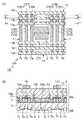
以下、本発明の第1実施形態に係る半導体装置SDの構成について、図1及び図2を用いて説明する。半導体装置SDは、光電変換装置100を含む。半導体装置SDの光電変換装置100における配線構造を上面から見た模式図を図1(A)に示す。図1(B)は、図1(A)の(A−A’,E−E’,A’’−A’’’)断面を示す図である。図1(B)では、便宜的に、A−A’断面とE−E’断面とA’’−A’’’断面とを繋げて示している。図2(A)は、図1(A)の(B−B’,E−E’,B’’−B’’’)断面を示す図である。図2(A)では、便宜的に、B−B’断面とE−E’断面とB’’−B’’’断面とを繋げて示している。図2(C)は、図1(A)の(C−C’,E−E’,C’’−C’’’)断面を示す図である。図2(C)では、便宜的に、C−C’断面とE−E’断面とC’’−C’’’断面とを繋げて示している。 Hereinafter, the configuration of the semiconductor device SD according to the first embodiment of the present invention will be described with reference to FIGS. 1 and 2. The semiconductor device SD includes a
半導体装置SDの光電変換装置100は、半導体基板SB及び多層配線構造MLを備える。半導体基板SBのウエル領域1には、複数の光電変換部2が2次元状に配されている。各光電変換部2は、光に応じた電荷を発生させる。光電変換部2は、例えば、フォトダイオードである。半導体基板SBのウエル領域1には、MOSトランジスタにおけるソース電極又はドレイン電極となる拡散層5が配されている。また、半導体基板SBには、素子分離部4が配されている。素子分離部4は、半導体基板SBにおけるアクティブ領域を規定するとともに、複数の光電変換部2を電気的に分離したり、複数のMOSトランジスタを電気的に分離したりする。 The
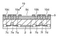
多層配線構造MLは、半導体基板SBの上に配されており、次の構成要素を含む。MOSトランジスタにおけるゲート電極3は、半導体基板SBの表面における2つの拡散層(ソース電極及びドレイン電極)5の上に配されている。ゲート電極3は、例えば、ポリシリコンで形成されており、ライン(ポリシリコンライン)とすることもできる。絶縁膜6は、半導体基板SB及びゲート電極3を覆っており、その上面が平坦化されている。第1の配線層7は、絶縁膜6の上に配されている。第1の配線層7は、例えば、アルミニウムを主成分とする金属又は金属間化合物で形成されている。第1の配線層7は、複数の第1の導電ライン7a〜7fを含む。複数の第1の導電ライン7a〜7fのうち第1の導電ライン7aと第1の導電ライン7bとは、それぞれ、光電変換部2の上方における開口領域ORを規定する。絶縁膜8は、第1の配線層7における複数の第1の導電ライン7a〜7fを覆っている。絶縁膜9は、絶縁膜8を覆っている。絶縁膜9は、絶縁膜8の研磨に対して耐性を有しており、第1の導電ライン上の層間絶縁膜を研磨・平坦化する際に研磨停止層としての役割を果たす。絶縁膜9は、複数の第1の導電ライン7a〜7fのそれぞれの上方に位置する開口と光電変換部2の上方に位置する開口とを有する。絶縁膜9は、絶縁膜8、絶縁膜11と比較して屈折率が高く、それらとの界面における光の反射を低減する役目を果たす。絶縁膜11は、絶縁膜9を覆っている。第2の配線層13は、絶縁膜8、絶縁膜9、及び絶縁膜11の上に配されている。第2の配線層13は、例えば、アルミニウムを主成分とする金属又は金属間化合物で形成されている。第2の配線層13は、複数の第2の導電ライン13a〜13fを含む。複数の第2の導電ライン13a〜13fのうち第2の導電ライン13aと第2の導電ライン13bとは、それぞれ、光電変換部2の上方における開口領域ORを規定する。複数の第2の導電ライン13a〜13fのそれぞれは、半導体基板SBの表面SBaに垂直な方向から透視した場合に複数の第1の導電ライン7a〜7fのそれぞれと交差するように延びている。絶縁膜14は、絶縁膜8、絶縁膜9、絶縁膜11、及び第2の配線層13を覆っており、その上面が平坦化されている。第3の配線層15は、絶縁膜14の上に配されている。 The multilayer wiring structure ML is arranged on the semiconductor substrate SB and includes the following components. The
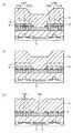
ここで、図1(A)、(B)及び図2(A)に示すように、複数の交差する領域CR1〜CR12のうち交差する領域CR1,CR2には、プラグ12a及び12bが配されている。プラグ12aは、第1の導電ライン7eと第2の導電ライン13aとを電気的に接続する役割を果たす。プラグ12bは、第1の導電ライン7fと第2の導電ライン13aとを電気的に接続する役割を果たす。プラグ12a、12bは、例えば、タングステンを主成分とする金属又は金属間化合物で形成されている。複数の交差する領域CR1〜CR12のうち残りの交差する領域CR3〜CR12には、エアギャップ10が設けられている。すなわち、絶縁膜8及び絶縁膜9は、複数の交差する領域CR3〜CR12のそれぞれにエアギャップ10を有する。エアギャップ10は、第1の導電ラインと第2の導電ラインとが交差していない領域に設けられていない。エアギャップ10は、真空空間をなしている、あるいは、空気が満たされている。これにより、エアギャップ10の誘電率は、約1であり、絶縁膜(例えば、SiO2)又はSiN)の誘電率より大幅に低減されている。すなわち、第1の導電ラインと第2の導電ラインとの間における寄生容量であるライン間容量が大きな箇所にエアギャップ10を設け、ライン間容量が小さな箇所にエアギャップ10を設けないようにするので、ライン間容量を効果的にかつ効率的に低減することができる。ここで、エアギャップ10に関する構成を、図2(B)を用いて詳細に説明する。図2(B)は、図2(A)の断面における領域Dを拡大した図である。第1の導電ライン7aと第2の導電ライン13cとの交差する領域CR9に設けられたエアギャップ10における第2の導電ライン13cに沿った方向の幅W10は、第1の導電ライン7aの幅W7a以下である。また、図示しないが、エアギャップ10における第1の導電ライン7aに沿った方向の幅は、第2の導電ライン13cの幅以下である。これに応じて、エアギャップ10の4つの側方では、支柱27が絶縁膜6と絶縁膜11との間を支えている。支柱27には、絶縁膜8及び絶縁膜9が含まれている。これにより、エアギャップ10の周囲における機械的強度、すなわち、多層配線構造MLの機械的強度の低下が抑制されている。このように、本実施形態では、半導体装置SDにおいて、多層配線構造MLにおけるライン間容量を低減しながら、多層配線構造MLの機械的強度の低下を抑制することができる。なお、上記では、光電変換装置100を中心に説明しているため、絶縁膜9が光電変換部2の上方に開口を有するものとしているが、光電変換装置以外の半導体装置の場合にはこの構成は不要である。Here, as shown in FIGS. 1A, 1B, and 2A, plugs 12a and 12b are arranged in crossing regions CR1 and CR2 among a plurality of crossing regions CR1 to CR12. Yes. The
次に、本発明の第1実施形態に係る半導体装置SDの製造方法について、図3〜図11を用いて説明する。図3、4、6に示す断面は、図1(B)の断面に対応した断面である。図5は、図4の工程における平面図である。図7(A)〜(C)に示す断面は、それぞれ、図1(B)、図2(A)、(C)の断面に対応した断面である。図8は、図7の工程における平面図である。図9(A)〜(C)に示す断面は、それぞれ、図1(B)、図2(A)、(C)の断面に対応した断面である。図10は、図9の工程における平面図である。図11(A)〜(C)に示す断面は、それぞれ、図1(B)、図2(A)、(C)の断面に対応した断面である。 Next, a method for manufacturing the semiconductor device SD according to the first embodiment of the present invention will be described with reference to FIGS. The cross sections shown in FIGS. 3, 4, and 6 correspond to the cross section of FIG. FIG. 5 is a plan view in the process of FIG. The cross sections shown in FIGS. 7A to 7C are cross sections corresponding to the cross sections of FIGS. 1B, 2A, and 2C, respectively. FIG. 8 is a plan view in the step of FIG. The cross sections shown in FIGS. 9A to 9C are cross sections corresponding to the cross sections of FIGS. 1B, 2A, and 2C, respectively. FIG. 10 is a plan view in the step of FIG. 11A to 11C are cross sections corresponding to the cross sections of FIGS. 1B, 2A, and 2C, respectively.
図3(A)の工程では、半導体基板SBに素子分離部4を形成した後に、半導体基板SBの表面SBaにおける素子分離部4により規定されたアクティブ領域の上に、ゲート電極3を形成する。そして、ゲート電極3をマスクとして半導体基板SBにイオン注入を行うことにより、半導体基板SBのウエル領域1(アクティブ領域)に光電変換部2及び拡散層5を形成する。ゲート電極3と拡散層5とはMOSトランジスタを構成する。その後、半導体基板SB及びゲート電極3を覆うように絶縁膜6を形成する。CMP法を用いて絶縁膜6を研磨することにより、絶縁膜6の上面を平坦化する。次いで、例えば拡散層5の表面を露出するように、絶縁膜6にスルーホール(図示せず)を形成し、そのスルーホールに金属(例えばタングステン)を埋め込むことにより、プラグ(図示せず)を形成する。そして、絶縁膜6の上に金属積層膜(例えば、TiN膜/AlCu合金膜/TiN膜の積層膜)における各膜をスパッタリング法により順次成膜した後、フォトリソグラフィー工程とドライエッチング工程とを経て第1の配線層7のパターンを形成する。すなわち、半導体基板SBの上方に複数の第1の導電ライン7a〜7fを形成する(第1の工程)。次に、高密度プラズマCVD法を用いて第1の配線層7(複数の第1の導電ライン7a〜7f)を覆うように絶縁膜8を形成する(第2の工程)。絶縁膜8は、例えばSiO2で形成する。その後、プラズマCVD法を用いて、絶縁膜8を覆うように絶縁膜9を形成する。絶縁膜9は、例えばSiNで形成する。続いて、プラズマCVD法を用いて、絶縁膜9を覆うように絶縁膜17を形成する。絶縁膜17は、研磨の犠牲膜となるべき膜である。絶縁膜17は、例えばSiO2で形成する。In the step of FIG. 3A, after the
図3(B)の工程では、CMP法を用いて、絶縁膜9の上面9aが露出するまで、絶縁膜17、絶縁膜9、及び絶縁膜8を研磨する。これにより、絶縁膜8における第1の導電ラインの上に位置する部分8aを第1の導電ラインの幅以下の幅で露出させる。言い換えると、絶縁膜9における第1の導電ラインの上に位置する(スリット状の)開口9bを第1の導電ラインの幅以下の幅で形成する。それとともに、絶縁膜8における部分8aの表面8a1と絶縁膜9の上面9aとを含む平坦な上面を得る。絶縁膜9(例えばSiN膜)の研磨速度は、絶縁膜17(例えばSiO2膜)の研磨速度の1/3以下である。すなわち、絶縁膜9は、絶縁膜17の研磨に対して耐性を有する。このため、絶縁膜9は研磨停止層として機能するので、絶縁膜8を過度に研磨することなくかつ第1の導電ラインを研磨することなく絶縁膜17を選択的に研磨して平坦化処理を終了することができる。絶縁膜9の膜厚は、研磨停止層として機能するのに十分な膜厚の下限値以上でありかつその上面9aと同じ高さに上記の部分8aが位置するような膜厚の上限値以下である。なお、図3(A)に示すように研磨前は第1の導電ラインの上部に絶縁膜8及び絶縁膜9が凸形状に形成されているが、その凸形状の部分は研磨の過程で除去され平坦化後に残らない。In the step of FIG. 3B, the insulating
図3(C)の工程では、フォトリソグラフィー工程を経て、絶縁膜9の上にエッチングマスク28を形成する。エッチングマスク28は、光電変換部2の上方の領域に開口28gを有し、溝19(図5参照)を形成すべき領域に開口28a〜28dを有する。一方、エッチングマスク28は、溝19を形成すべきでない領域(図5における部分8a参照)を覆っている。エッチングマスク28は、例えば、フォトレジスト樹脂で形成する。 In the process of FIG. 3C, an
図4の工程では、エッチングマスク28と上記の研磨された絶縁膜9とをマスクとして絶縁膜8における第1の配線の上の部分8aをエッチングする。各溝の幅が各第1の配線の幅以下になるように、絶縁膜8に複数の第1の配線7a〜7fを露出する複数の溝19a〜19f’(図5参照)を形成する(第3の工程)。各溝19a〜19f’は、その一部分がエアギャップ10になるべき溝である。図4及び図5に示されるように、複数の溝19a〜19f’は、複数の第1の配線7a〜7fのうち後述のプラグ12a,12b(図6(C)参照)が配されるべき領域CR1,CR2を除いた領域における複数の第1の配線7a〜7fの上に形成される。上記のように、各溝19a〜19f’の幅は各第1の配線7a〜7fの幅以下である。ここで、例えば、絶縁膜8がSiO2で形成されている場合、SiO2が選択的にエッチングされるエッチングガス(例えば、C4F8+CO+Ar+O2)を用いてドライエッチングを実施する。この場合、絶縁膜9に対する絶縁膜8のエッチング選択比(エッチング速度比)が大きくなる。すなわち、絶縁膜9は、絶縁膜8のエッチングに対して耐性を有する。これにより、絶縁膜8における第1の配線の上に位置する部分8aの膜厚が絶縁膜9の膜厚に比べて厚くても、絶縁膜8を選択的にエッチングすることができる。その後、エッチングマスク28を介して絶縁膜9が選択的にエッチングされる条件でドライエッチングを実施する。例えば、絶縁膜9がSiNで形成されている場合、SiNが選択的にエッチングされるエッチングガス(例えば、CH2F2+CO+O2)を用いてドライエッチングを実施する。これにより、絶縁膜9における光電変換部2の上方に位置した部分9g(図3(C)参照)を除去する。In the process of FIG. 4, the
なお、図4の工程では、エッチングマスク28(図3(C)参照)を介してドライエッチングを実施することにより、絶縁膜9における部分9gと絶縁膜8における部分8aとを同時に除去しても良い。例えば、SiO2が選択的にエッチングされるエッチングガス(例えば、C4F8+CO+Ar+O2)とSiNが選択的にエッチングされるエッチングガス(例えば、CH2F2+CO+O2)との混合ガスを用いてドライエッチングを実施する。これにより、絶縁膜8がSiO2で形成され、絶縁膜9がSiNで形成されている場合、絶縁膜9に対する絶縁膜8のエッチング選択比(エッチング速度比)が1に近くなる。この場合でも、エッチングの異方性が高ければ、絶縁膜8における部分8aの除去とエアギャップ10になるべき溝19の形成とを同時に達成することができる。これにより、光電変換部2上に残存する研磨停止層(絶縁膜9)を除去する工程と溝19を形成する工程とを共通化できる。In the process of FIG. 4, even if the
図6(A)の工程では、プラズマCVD法を用いて、複数の溝19a〜19f’のそれぞれに有機系絶縁体(第1の絶縁体)18aを埋め込むとともに絶縁膜9の開口9cに有機系絶縁体18bを埋め込む。また、絶縁膜9を覆うように、有機系絶縁膜18を形成する(第4の工程)。有機系絶縁体18a及び有機系絶縁体18bと有機系絶縁膜18とは、連続的に形成される。有機系絶縁体18a及び有機系絶縁体18bと有機系絶縁膜18とは、例えば、SiOCで形成される。 In the process of FIG. 6A, an organic insulator (first insulator) 18a is embedded in each of the plurality of
図6(B)の工程では、CMP法を用いて、絶縁膜9の上面9aが露出するまで、有機系絶縁膜18、絶縁膜9、及び絶縁膜8を研磨する。これにより、有機系絶縁膜18が除去されて、有機系絶縁体18aが複数の溝19a〜19f’の中に残り、有機系絶縁体18bが開口9cの中に残った状態になる。このとき、絶縁膜8の研磨速度と絶縁膜9の研磨速度とが、それぞれ、有機系絶縁膜18の研磨速度の1/5以下である。すなわち、絶縁膜9は、有機系絶縁膜18の研磨に対して耐性を有する。このため、絶縁膜9は研磨停止層として機能するので、有機系絶縁体18a及び有機系絶縁体18bを残しながら有機系絶縁膜18を選択的に研磨して平坦化処理を終了することができる。続いて、プラズマCVD法を用いて、絶縁膜8、絶縁膜9、及び有機系絶縁体18aを覆うように、絶縁膜11を形成する。絶縁膜11は、例えば、SiO2で形成する。In the process of FIG. 6B, the organic insulating
図6(C)の工程では、例えば領域CR1,CR2における第1の導電ライン7e,7fの表面を露出するように、絶縁膜8及び絶縁膜11にスルーホール(図示せず)を形成する。そのスルーホールに埋め込まれるとともに絶縁膜11を覆うように金属層を形成する。金属層は、例えばタングステンで形成する。そして、絶縁膜11の表面が露出されるまで金属層を研磨することにより、プラグ12a,12bを形成する。このとき、絶縁膜11における表面近傍の部分も研磨される。その後、絶縁膜11の上に金属積層膜(例えば、TiN膜/AlCu合金膜/TiN膜の積層膜)における各膜をスパッタリング法により順次成膜する。 In the process of FIG. 6C, through holes (not shown) are formed in the insulating
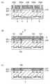
図7(A)〜(C)は、同じ工程における断面を示す。図7の工程では、フォトリソグラフィー工程とドライエッチング工程とを経て絶縁膜11と金属積層膜とをパターニングすることにより、第2の配線層13のパターンを形成する。すなわち、絶縁膜8、有機系絶縁体18a、及び絶縁膜11の上に、複数の第1の導電ライン7a〜7fと交差するように複数の第2の導電ライン13a〜13fを形成する(第5の工程)。有機系絶縁体18aの上面の一部を覆うように複数の第2の導電ライン13a〜13fを形成する。このとき、図7(C)及び図8に示すように、ドライエッチング工程におけるオーバーエッチング処理にて、第2の導電ラインを配しない領域の絶縁膜11も除去し、有機系絶縁体18aを露出させる。第2の導電ラインを配しない領域は、図1に示す開口領域ORを含む。一方、図7(A)、(B)及び図8に示すように、ドライエッチング工程において第2の導電ラインがマスクとして機能するため、第2の導電ラインを配する領域の絶縁膜11は除去されずに残っており有機系絶縁体18aを覆っている。 7A to 7C show cross sections in the same process. In the process of FIG. 7, the pattern of the
図9(A)〜(C)は、同じ工程における断面を示す。図9の工程では、有機系絶縁体18aの絶縁膜8、絶縁膜9、及び第2の導電ラインのそれぞれに対するエッチング選択比が高くなる条件で等方性エッチングを行うことにより、有機系絶縁体18aを複数の溝19a〜19f’から除去する(第6の工程)。有機系絶縁体18aの上面のうち半導体基板SBの表面SBaに垂直な方向から見た場合に第2の導電ラインが重ならない部分が露出した状態で等方性エッチングを行うことにより、有機系絶縁体18aを複数の溝19a〜19f’のそれぞれから除去する。有機系絶縁体18aの絶縁膜8、絶縁膜9、及び第2の導電ラインのそれぞれに対するエッチング選択比は、例えばCF4+O2をエッチングガスとして用いた場合、1/20である。このため、有機系絶縁体18aを選択的にエッチングすることができる。また、ドライエッチングが等方性であるため、図9(A)、(B)に示すように、第2の導電ライン13a,13cの下にある有機系絶縁体18aも、回り込むエッチングガス(例えばCF4+O2)によって効果的に除去される。9A to 9C show cross sections in the same process. In the step of FIG. 9, isotropic etching is performed under the condition that the etching selection ratio of the
なお、有機系絶縁体18aを等方性ドライエッチングにより除去するために、有機系絶縁体18aを露出させる工程を第2の配線層13のパターニングのためのドライエッチング時のオーバーエッチングを利用して実施することができる。この場合、有機系絶縁体18aを露出させる工程と第2の配線層13をパターニングする工程とを共通化することができる。 In order to remove the
図11(A)〜(C)は、同じ工程における断面を示す。図11の工程では、高密度プラズマCVD法を用いて、複数の溝19a〜19f’における半導体基板の表面に垂直な方向から見た場合に第2の導電ライン13a〜13fに重ならない部分に絶縁体(第2の絶縁体)14aを埋め込む(図11(C)参照)。また、複数の第2の導電ライン13a〜13fを覆うように絶縁膜14を形成する。絶縁体14aと絶縁膜14とは、連続的に形成される。絶縁膜14は、例えば、SiO2で形成される。すなわち、複数の溝19a〜19f’内(溝内)の複数の第1の導電ラインと第2の導電ラインとの交差する複数の領域における一部の領域をエアギャップ10として残すように、複数の溝19a〜19f’に絶縁体(第2の絶縁体)14aを埋め込む。このとき、複数の溝19a〜19f’のそれぞれにおける半導体基板SBの表面SBaに垂直な方向から見た場合に第2の導電ラインが重ならない部分に第2の絶縁体を埋め込む(第7の工程)。例えば、図11(A)、(B)に示すように、複数の交差する領域CR1〜CR12(図1参照)のうち、交差する領域CR1,CR2にプラグ12a、12bが配され、残りの複数の交差する領域CR3〜CR12のそれぞれにエアギャップ10が形成されている。このとき、各第2の導電ラインの下にある空間にはCVDガスが回り込み難いために、真空空間をなしている、あるいは、空気が満たされている状態を保持したままのエアギャップ10が第2の導電ラインの幅以下の幅で形成される。すなわち、エアギャップ10における第1の導電ラインに沿った方向の幅が第2の導電ラインの幅以下になるように、エアギャップ10は形成される。一方、エアギャップ10における第2の導電ラインに沿った方向の幅は、図4の工程で各溝の幅が各第1の導電ラインの幅以下になるように形成されていることに応じて、第1の導電ラインの幅以下になっている。次に、CMP法を用いて、絶縁膜14を研磨することにより絶縁膜14の上面を平坦化する。次いで、例えば第2の導電ラインの表面を露出するように、絶縁膜14にスルーホール(図示せず)を形成し、そのスルーホールに金属(例えばタングステン)を埋め込むことにより、プラグ(図示せず)を形成する。その後、絶縁膜14の上に金属積層膜(例えば、TiN膜/AlCu合金膜/TiN膜の積層膜)における各膜をスパッタリング法により順次成膜し、その後にフォトリソグラフィー工程とドライエッチング工程とを経て第3の配線層(図示せず)のパターンを形成する。11A to 11C show cross sections in the same process. In the process of FIG. 11, the high density plasma CVD method is used to insulate portions that do not overlap the second
ここで、図2(B)に示すように、第2の配線層13と絶縁膜6との間は、絶縁膜11を介して、絶縁膜8と絶縁膜9とに含まれる支柱27によって支えられる構造になっている。このため、第2の配線層13が図2(B)における横方向に長くなった場合でも、多層配線構造MLの全体としての機械的強度は保持され、後の工程におけるCMP等による応力がかかった場合にも多層配線構造MLが破壊されにくい。また、第1の導電ラインと第2の導電ラインとの交差する領域(例えば、交差する領域CR3〜CR12)にエアギャップ10が設けられているので、第1の導電ラインと第2の導電ラインとのライン間容量が低減されている。このように、本実施形態に係る製造方法によれば、多層配線構造MLにおけるライン間容量を低減しながら、多層配線構造MLの機械的強度の低下を抑制することができる半導体装置SDを得ることができる。 Here, as shown in FIG. 2B, the space between the
次に、本発明の光電変換装置を適用した撮像システムの一例を図12に示す。撮像システム90は、図12に示すように、主として、光学系、撮像装置86及び信号処理部を備える。光学系は、主として、シャッター91、レンズ92及び絞り93を備える。撮像装置86は、光電変換装置100を含む。信号処理部は、主として、撮像信号処理回路95、A/D変換器96、画像信号処理部97、メモリ部87、外部I/F部89、タイミング発生部98、全体制御・演算部99、記録媒体88及び記録媒体制御I/F部94を備える。なお、信号処理部は、記録媒体88を備えなくても良い。シャッター91は、光路上においてレンズ92の手前に設けられ、露出を制御する。レンズ92は、入射した光を屈折させて、撮像装置86の光電変換装置100の撮像面に被写体の像を形成する。絞り93は、光路上においてレンズ92と光電変換装置100との間に設けられ、レンズ92を通過後に光電変換装置100へ導かれる光の量を調節する。撮像装置86の光電変換装置100は、光電変換装置100の撮像面に形成された被写体の像を画像信号に変換する。撮像装置86は、その画像信号を光電変換装置100から読み出して出力する。撮像信号処理回路95は、撮像装置86に接続されており、撮像装置86から出力された画像信号を処理する。A/D変換器96は、撮像信号処理回路95に接続されており、撮像信号処理回路95から出力された処理後の画像信号(アナログ信号)を画像信号(デジタル信号)へ変換する。画像信号処理部97は、A/D変換器96に接続されており、A/D変換器96から出力された画像信号(デジタル信号)に各種の補正等の演算処理を行い、画像データを生成する。この画像データは、メモリ部87、外部I/F部89、全体制御・演算部99及び記録媒体制御I/F部94などへ供給される。メモリ部87は、画像信号処理部97に接続されており、画像信号処理部97から出力された画像データを記憶する。外部I/F部89は、画像信号処理部97に接続されている。これにより、画像信号処理部97から出力された画像データを、外部I/F部89を介して外部の機器(パソコン等)へ転送する。タイミング発生部98は、撮像装置86、撮像信号処理回路95、A/D変換器96及び画像信号処理部97に接続されている。これにより、撮像装置86、撮像信号処理回路95、A/D変換器96及び画像信号処理部97へタイミング信号を供給する。そして、撮像装置86、撮像信号処理回路95、A/D変換器96及び画像信号処理部97がタイミング信号に同期して動作する。全体制御・演算部99は、タイミング発生部98、画像信号処理部97及び記録媒体制御I/F部94に接続されており、タイミング発生部98、画像信号処理部97及び記録媒体制御I/F部94を全体的に制御する。記録媒体88は、記録媒体制御I/F部94に取り外し可能に接続されている。これにより、画像信号処理部97から出力された画像データを、記録媒体制御I/F部94を介して記録媒体88へ記録する。以上の構成により、光電変換装置100において良好な画像信号が得られれば、良好な画像(画像データ)を得ることができる。 Next, an example of an imaging system to which the photoelectric conversion device of the present invention is applied is shown in FIG. As shown in FIG. 12, the
次に、本発明の第2実施形態に係る半導体装置SD200を、図13〜図21を用いて説明する。以下では、第1実施形態と異なる部分を中心に説明する。 Next, a semiconductor device SD200 according to the second embodiment of the present invention will be described with reference to FIGS. Below, it demonstrates centering on a different part from 1st Embodiment.
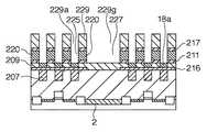
図13に示すように、半導体装置SD200は、光電変換装置200を含む。図13は、半導体装置SD200における図1(B)の断面に対応する断面を示す図である。半導体装置SD200の光電変換装置200は、多層配線構造ML200を備える。多層配線構造ML200は、デュアルダマシン構造を有している。多層配線構造ML200は、次の構成要素を含む点で第1実施形態と異なる。第1の配線層207は、絶縁膜206の中に配されている。第1の配線層207は、例えば、銅を主成分とする金属又は金属間化合物で形成されている。第1の配線層207における複数の第1の導電ライン207a〜207fは、それぞれ、シングルダマシン法にて、絶縁膜206に形成された溝に埋め込まれている。拡散抑制膜(拡散バリア膜)216は、第1の配線層207を覆っている。拡散抑制膜216は、第1の配線層207の材料(例えば銅)が絶縁膜209中へ拡散することを抑制する。第2の配線層213は、絶縁膜220の中に配されている。第2の配線層213は、例えば、銅を主成分とする金属又は金属間化合物で形成されている。第2の配線層213における複数の第2の導電ライン213a〜213fは、デュアルダマシン法にて、絶縁膜220に形成された溝に上記の材料が埋め込まれることにより形成されている。絶縁膜211は、デュアルダマシン法における第2の導電ラインを埋め込むための溝を形成するエッチングを行う際のエッチング停止層としての役割を果たす。拡散抑制膜(拡散バリア膜)217は、第2の配線層213を覆っている。拡散抑制膜217は、第2の配線層213の材料(例えば銅)が絶縁膜223中へ拡散することを抑制する。拡散抑制膜216、絶縁膜211、及び拡散抑制膜217は、それぞれ、光電変換部2の上方に位置する部分に開口を有する。 As illustrated in FIG. 13, the semiconductor device SD200 includes a
ここで、複数の交差する領域CR1〜CR12(図1(A)、(B)及び図2(A)参照)のうち交差する領域CR1,CR2には、プラグ212a及び212bが配されている。プラグ212a及び212bは、それぞれ、例えば、銅を主成分とする金属又は金属間化合物で形成されている。プラグ212a及び212bは、デュアルダマシン法にて、絶縁膜211、絶縁膜209、及び拡散抑制膜216に形成された穴に上記の材料が埋め込まれることにより形成されている。一方、複数の交差する領域CR1〜CR12のうち残りの交差する領域CR3〜CR12にエアギャップ10が設けられている点は、第1実施形態と同様である。エアギャップ10の4つの側方では、支柱227が絶縁膜206と絶縁膜211との間を支えている。支柱227は、拡散抑制膜216及び絶縁膜209に含まれている。 Here, plugs 212a and 212b are arranged in the intersecting regions CR1 and CR2 among the plurality of intersecting regions CR1 to CR12 (see FIGS. 1A, 1B, and 2A). The
また、半導体装置SD200の製造方法が、図14〜図21に示すように、次の点で第1実施形態と異なる。図14、16に示す断面は、図1(B)の断面に対応した断面である。図15は、図14(C)の工程における平面図である。図18、19に示す断面は、それぞれ、図2(C)、図1(B)の断面に対応した断面である。図17は、図18、19の工程における平面図である。図20(B)、(C)に示す断面は、それぞれ、図2(C)、図1(B)の断面に対応した断面である。図20(A)は、図20(B)、(C)の工程における平面図である。図21(B)、(C)に示す断面は、それぞれ、図2(C)、図1(B)の断面に対応した断面である。図21(A)は、図21(B)、(C)の工程における平面図である。 Further, as shown in FIGS. 14 to 21, the manufacturing method of the semiconductor device SD200 differs from the first embodiment in the following points. The cross section shown in FIGS. 14 and 16 is a cross section corresponding to the cross section of FIG. FIG. 15 is a plan view in the step of FIG. The cross sections shown in FIGS. 18 and 19 are cross sections corresponding to the cross sections of FIGS. 2C and 1B, respectively. FIG. 17 is a plan view in the process of FIGS. The cross sections shown in FIGS. 20B and 20C are cross sections corresponding to the cross sections of FIGS. 2C and 1B, respectively. FIG. 20A is a plan view in the steps of FIGS. 20B and 20C. The cross sections shown in FIGS. 21B and 21C correspond to the cross sections of FIGS. 2C and 1B, respectively. FIG. 21A is a plan view in the steps of FIGS. 21B and 21C.
図14(A)の工程では、絶縁膜206の上面を平坦化した後、ダマシン法により第1の配線層207を形成する。すなわち、第1の配線層207の材料(例えば、銅を主成分とする金属又は金属間化合物)を埋め込むための溝を絶縁膜206に形成し、その材料をその溝に埋め込むことにより、第1の配線層207を形成する。その後、プラズマCVD法を用いて、第1の配線層207を覆うように、拡散抑制膜216を形成する。拡散抑制膜216は、例えば、SiNで形成する。その後に、フォトリソグラフィー工程を経て、拡散抑制膜216における光電変換部2の上方に位置した部分をドライエッチング法により除去する。次に、プラズマCVD法を用いて、絶縁膜206及び拡散抑制膜216を覆うように絶縁膜209を形成する。絶縁膜209は、例えば、SiO2で形成する。そして、絶縁膜209の上面に生じた段差をCMP法にて研磨して平坦化する。そして、フォトリソグラフィー工程を経て、絶縁膜209の上にエッチングマスク228を形成する。エッチングマスク228は、溝19(図5参照)を形成すべき領域に開口228a〜228dを有する。14A, after planarizing the upper surface of the insulating
図14(B)の工程では、エッチングマスク228(図14(A)参照)を介して絶縁膜209における第1の導電ラインの上の部分をエッチングする。これにより、各溝の幅が各第1の導電ラインの幅以下になるように、絶縁膜209に複数の溝19a〜19f’(図5参照)を形成する点は、第1実施形態と同様である。その後、図6(A)の工程と同様の処理を行う。 In the step of FIG. 14B, the portion of the insulating
図14(C)の工程では、図6(B)の工程と同様の平坦化処理を行う。これにより、図15に示すように、有機系絶縁体18aを露出させる。続いて、プラズマCVD法を用いて、絶縁膜209及び有機系絶縁体18aを覆うように、絶縁膜211を形成する。絶縁膜211は、例えば、SiNで形成する。絶縁膜211は、デュアルダマシン法における第2の導電ラインを埋め込むための穴を形成するエッチングを行う際のエッチング停止層としての役割を果たす。 In the step of FIG. 14C, the same planarization process as in the step of FIG. 6B is performed. This exposes the
図16の工程では、プラズマCVD法を用いて、絶縁膜(第2の絶縁膜)220を絶縁膜211の上に形成する。フォトリソグラフィー工程を経て、デュアルダマシン法におけるプラグ212a,212bを埋め込むための第1の穴224を絶縁膜220、絶縁膜211、絶縁膜209、及び絶縁膜216に形成する。また、フォトリソグラフィー工程を経て、デュアルダマシン法における第2の導電ラインを埋め込むための第2の溝226を絶縁膜220に形成する。その後、Ta膜と導電体シード膜とをスパッタリング法により形成し、メッキ法による導電体の埋め込みを第1の穴224及び第2の溝226に対して行う。導電体は、例えば、銅を主成分とする金属又は金属間化合物で形成する。そして、CMP法による研磨・平坦化を行うことにより、プラグ212と第2の溝226に対応した第2の配線層213とを形成する。次に、プラズマCVD法を用いて、第2の配線層213及び絶縁膜220を覆うように拡散抑制膜217を形成する。拡散抑制膜217は、例えば、SiNで形成する。 In the process of FIG. 16, an insulating film (second insulating film) 220 is formed on the insulating
図18及び図19は、同じ工程における断面を示す。図18及び図19の工程では、フォトリソグラフィー工程を経て、拡散抑制膜217の上にエッチングマスク229を形成する。エッチングマスク229は、光電変換部2の上方の領域に開口229gを有し、有機系絶縁体18aを露出するための後述の第2の穴225を形成すべき領域に開口229aを有する。エッチングマスク229と第2の導電ラインとをマスクとして散抑制膜217、絶縁膜220、及び絶縁膜211をエッチングする。これにより、有機系絶縁体18aの上面のうち半導体基板の表面SBaに垂直な方向から見た場合に第2の導電ラインが重ならない部分を露出するように複数の第2の穴225を、拡散抑制膜217、絶縁膜220、及び絶縁膜211に形成する(図17参照)。このとき、拡散抑制膜217、絶縁膜220、及び絶縁膜211のそれぞれにおける光電変換部2の上方に位置した部分も除去されて、第3の溝227が形成される。 18 and 19 show cross sections in the same process. 18 and 19, an
図20(A)〜(C)は、同じ工程における平面図及び断面図を示す。図20の工程では、有機系絶縁体18aの拡散抑制膜217、絶縁膜220、絶縁膜211、及び絶縁膜209のそれぞれに対するエッチング選択比が高くなる条件で第2の穴225を介して等方性エッチングを行う。これにより、有機系絶縁体18aを複数の溝19a〜19f’(図5参照)から除去する。このとき、拡散抑制膜216と絶縁膜209とは、それぞれ、有機系絶縁体18aの等方性ドライエッチングに対し高い耐性を有しているため。有機系絶縁体18aを選択的にエッチングすることが容易である(図20(B)参照)。また、ドライエッチングが等方性であるため、第2の配線層213の下にある有機系絶縁体18aは、回り込むエッチングガスによって除去される(図20(C)参照)。 20A to 20C are a plan view and a cross-sectional view in the same process. In the process of FIG. 20, the
図21の工程では、高密度プラズマCVD法を用いて、絶縁体(第2の絶縁体)223aを複数の第2の穴225に埋め込むとともに絶縁体223bを第3の溝227に埋め込む。また、拡散抑制膜217を覆うように絶縁膜223を形成する。すなわち、複数の溝19a〜19f’における第1の導電ラインと第2の導電ラインとの交差する複数の領域における一部の領域をエアギャップ10として残すように、複数の第2の穴225を介して複数の溝19a〜19f’に絶縁体223aを埋め込む。このとき、各第2の導電ラインの下にある空間にはCVDガスが回り込み難いために、真空空間をなしている、あるいは、空気が満たされている状態を保持したままのエアギャップ10が第2の導電ラインの幅以下の幅で形成される。すなわち、エアギャップ10における第1の導電ラインに沿った方向の幅が第2の導電ラインの幅以下になるように、エアギャップ10は形成される。一方、エアギャップ10における第2の導電ラインに沿った方向の幅は、図14(B)の工程で各溝の幅が各第1の導電ラインの幅以下になるように形成されていることに応じて、第1の導電ラインの幅以下になっている。 In the step of FIG. 21, the insulator (second insulator) 223a is embedded in the plurality of
なお、半導体装置の製造方法において、エッチング停止層および拡散抑制膜のそれぞれにおける光電変換部の上方に位置する部分を除去する処理を、エアギャップを形成する工程を利用して実施することができる。このため、エッチング停止層および拡散抑制膜の部分を除去する処理とエアギャップを形成する処理とを別の工程で行う場合に比べて、工程数を削減できる。 In the method for manufacturing a semiconductor device, the process of removing the portions of the etching stopper layer and the diffusion suppression film that are located above the photoelectric conversion portion can be performed using a step of forming an air gap. For this reason, the number of processes can be reduced as compared with the case where the process of removing the portions of the etching stopper layer and the diffusion suppressing film and the process of forming the air gap are performed in separate processes.
Claims (6)
Translated fromJapanese前記半導体基板の上に配された多層配線構造と、
を備え、
前記多層配線構造は、
複数の第1の導電ラインと、
前記複数の第1の導電ラインを覆う絶縁膜と、
前記複数の第1の導電ラインと交差するように前記絶縁膜の上に配された第2の導電ラインと、
を含み、
前記絶縁膜は、前記複数の第1の導電ラインと前記第2の導電ラインとが交差する複数の領域における少なくとも一部の領域にギャップを有し、前記光電変換部の上にギャップを有さず、
前記第2の導電ラインに沿った方向における前記ギャップの幅は、前記第1の導電ラインの幅以下である
ことを特徴とする半導体装置。A semiconductor substrateincluding a photoelectric conversion unit ;
A multilayer wiring structure disposed on the semiconductor substrate;
With
The multilayer wiring structure is
A plurality of first conductive lines;
An insulating film covering the plurality of first conductive lines;
A second conductive line disposed on the insulating film so as to intersect the plurality of first conductive lines;
Including
The insulating film has a gap in at least a part of a plurality of regions where the plurality of first conductive lines and the second conductive line intersect, and has agap on the photoelectric conversion unit. Without
The semiconductor device according to claim 1, wherein a width of the gap in a direction along the second conductive line is equal to or smaller than a width of the first conductive line.
ことを特徴とする請求項1に記載の半導体装置。2. The semiconductor device according to claim 1, wherein a width of the gap in a direction along the first conductive line is equal to or less than a width of the second conductive line.
前記半導体基板の上方に複数の第1の導電ラインを形成する第1の工程と、
前記複数の第1の導電ラインを覆うように絶縁膜を形成する第2の工程と、
前記絶縁膜に前記複数の第1の導電ラインの上面の一部を露出する複数の溝をそれぞれ前記第1の導電ラインの幅以下の幅で形成する第3の工程と、
前記複数の溝のそれぞれに第1の絶縁体を埋め込む第4の工程と、
前記絶縁膜及び前記第1の絶縁体の上に、前記複数の第1の導電ラインと交差するように第2の導電ラインを形成する第5の工程と、
前記第5の工程の後に、前記第1の絶縁体を前記複数の溝のそれぞれから除去する第6の工程と、
前記第6の工程の後に、前記複数の溝内の前記第1の導電ラインと前記第2の導電ラインとが交差する複数の領域における少なくとも一部の領域をギャップとして残すように、前記複数の溝のそれぞれにおける前記半導体基板の表面に垂直な方向から見た場合に前記第2の導電ラインが重ならない部分に第2の絶縁体を埋め込む第7の工程と、
を含み、
前記第2の導電ラインに沿った方向における前記ギャップの幅は、前記第1の導電ラインの幅以下である
ことを特徴とする半導体装置の製造方法。A method of manufacturing a semiconductor device having a semiconductor substrate,
A first step of forming a plurality of first conductive lines above the semiconductor substrate;
A second step of forming an insulating film so as to cover the plurality of first conductive lines;
A third step of forming, in the insulating film, a plurality of grooves exposing a part of the upper surfaces of the plurality of first conductive lines, each having a width equal to or smaller than a width of the first conductive line;
A fourth step of embedding a first insulator in each of the plurality of grooves;
A fifth step of forming a second conductive line on the insulating film and the first insulator so as to intersect the plurality of first conductive lines;
A sixth step of removing the first insulator from each of the plurality of grooves after the fifth step;
After the sixth step, the plurality of the plurality of regions are left as gaps in at least a part of the plurality of regions where the first conductive lines and the second conductive lines intersect in the plurality of grooves. A seventh step of embedding a second insulator in a portion where each of the grooves does not overlap the second conductive line when viewed from a direction perpendicular to the surface of the semiconductor substrate;
Including
The method of manufacturing a semiconductor device, wherein a width of the gap in a direction along the second conductive line is equal to or smaller than a width of the first conductive line.
ことを特徴とする請求項3に記載の半導体装置の製造方法。In the sixth step, the first insulator is exposed in a state where a portion of the upper surface of the first insulator that does not overlap the second conductive line when exposed from a direction perpendicular to the surface of the semiconductor substrate is exposed. Removing the first insulator from each of the plurality of grooves by performing isotropic etching under a condition that an etching selectivity ratio of the insulator to the insulating film and the second conductive line is increased. The method for manufacturing a semiconductor device according to claim3 , wherein:
前記絶縁膜及び前記第1の絶縁体の上に第2の絶縁膜を形成する工程と、
前記第2の絶縁膜に、前記複数の第1の導電ラインと交差するように第2の溝を形成する工程と、
前記第2の溝に導電体を埋め込むことにより、前記第2の溝に対応した前記第2の導電ラインを形成する工程と、
を含み、
前記第6の工程は、
前記第1の絶縁体の上面のうち前記半導体基板の表面に垂直な方向から見た場合に前記第2の導電ラインが重ならない部分を露出するように複数の穴を前記第2の絶縁膜に形成する工程と、
前記絶縁膜及び前記第2の導電ラインに対する前記第1の絶縁体のエッチング選択比が高くなる条件で前記複数の穴を介して等方性エッチングを行うことにより、前記第1の絶縁体を前記複数の溝のそれぞれから除去する工程と、
を含み、
前記第7の工程では、
前記複数の穴を介して前記複数の溝のそれぞれに前記第2の絶縁体を埋め込む
ことを特徴とする請求項3に記載の半導体装置の製造方法。The fifth step includes
Forming a second insulating film on the insulating film and the first insulator;
Forming a second groove in the second insulating film so as to intersect the plurality of first conductive lines;
Forming the second conductive line corresponding to the second groove by embedding a conductor in the second groove;
Including
The sixth step includes
A plurality of holes are formed in the second insulating film so as to expose a portion of the upper surface of the first insulator that does not overlap the second conductive line when viewed from a direction perpendicular to the surface of the semiconductor substrate. Forming, and
By performing isotropic etching through the plurality of holes under a condition in which the etching selectivity of the first insulator to the insulating film and the second conductive line is high, the first insulator is Removing from each of the plurality of grooves;
Including
In the seventh step,
The method of manufacturing a semiconductor device according to claim3 , wherein the second insulator is embedded in each of the plurality of grooves through the plurality of holes.
前記半導体基板は、光電変換部を含む
ことを特徴とする請求項3から5のいずれか1項に記載の半導体装置の製造方法。The semiconductor device includes a photoelectric conversion device,
6. The method of manufacturing a semiconductor device according to claim3 , wherein the semiconductor substrate includes a photoelectric conversion unit.
Priority Applications (5)
| Application Number | Priority Date | Filing Date | Title |
|---|---|---|---|
| JP2009137721AJP5491077B2 (en) | 2009-06-08 | 2009-06-08 | Semiconductor device and manufacturing method of semiconductor device |
| EP10161984.9AEP2261968B1 (en) | 2009-06-08 | 2010-05-05 | Method of manufacturing a semiconductor device |
| US12/782,889US8350300B2 (en) | 2009-06-08 | 2010-05-19 | Semiconductor device having air gaps in multilayer wiring structure |
| CN201010196500.9ACN101908525B (en) | 2009-06-08 | 2010-06-03 | Semiconductor device and method of manufacturing the same |
| US13/707,887US8748210B2 (en) | 2009-06-08 | 2012-12-07 | Method of manufacturing semiconductor device having air gaps in multilayer wiring structure |
Applications Claiming Priority (1)
| Application Number | Priority Date | Filing Date | Title |
|---|---|---|---|
| JP2009137721AJP5491077B2 (en) | 2009-06-08 | 2009-06-08 | Semiconductor device and manufacturing method of semiconductor device |
Publications (3)
| Publication Number | Publication Date |
|---|---|
| JP2010283307A JP2010283307A (en) | 2010-12-16 |
| JP2010283307A5 JP2010283307A5 (en) | 2012-07-26 |
| JP5491077B2true JP5491077B2 (en) | 2014-05-14 |
Family
ID=42712730
Family Applications (1)
| Application Number | Title | Priority Date | Filing Date |
|---|---|---|---|
| JP2009137721AExpired - Fee RelatedJP5491077B2 (en) | 2009-06-08 | 2009-06-08 | Semiconductor device and manufacturing method of semiconductor device |
Country Status (4)
| Country | Link |
|---|---|
| US (2) | US8350300B2 (en) |
| EP (1) | EP2261968B1 (en) |
| JP (1) | JP5491077B2 (en) |
| CN (1) | CN101908525B (en) |
Families Citing this family (11)
| Publication number | Priority date | Publication date | Assignee | Title |
|---|---|---|---|---|
| JP5422455B2 (en)* | 2010-03-23 | 2014-02-19 | パナソニック株式会社 | Solid-state imaging device |
| JP6184061B2 (en) | 2012-05-29 | 2017-08-23 | キヤノン株式会社 | Multilayer semiconductor device and electronic device |
| US8921901B1 (en)* | 2013-06-10 | 2014-12-30 | United Microelectronics Corp. | Stacked CMOS image sensor and signal processor wafer structure |
| CN114759051B (en)* | 2015-03-31 | 2025-09-12 | 索尼半导体解决方案公司 | Light detection device |
| JP6856974B2 (en)* | 2015-03-31 | 2021-04-14 | ソニーセミコンダクタソリューションズ株式会社 | Solid-state image sensor and electronic equipment |
| US10211146B2 (en) | 2016-05-12 | 2019-02-19 | Globalfoundries Inc. | Air gap over transistor gate and related method |
| US10157777B2 (en)* | 2016-05-12 | 2018-12-18 | Globalfoundries Inc. | Air gap over transistor gate and related method |
| KR102539779B1 (en)* | 2016-08-25 | 2023-06-07 | 소니 세미컨덕터 솔루션즈 가부시키가이샤 | Semiconductor device, image pickup device, and method for manufacturing semiconductor device |
| CN115812248A (en)* | 2020-07-13 | 2023-03-17 | 索尼半导体解决方案公司 | Wiring structure, method of manufacturing the same, and image forming apparatus |
| CN113644087A (en)* | 2021-08-10 | 2021-11-12 | 长江先进存储产业创新中心有限责任公司 | Phase change memory and manufacturing method thereof |
| US12341058B2 (en) | 2022-02-04 | 2025-06-24 | Globalfoundries Singapore Pte. Ltd. | Air gap through at least two metal layers |
Family Cites Families (22)
| Publication number | Priority date | Publication date | Assignee | Title |
|---|---|---|---|---|
| NL181611C (en)* | 1978-11-14 | 1987-09-16 | Philips Nv | METHOD FOR MANUFACTURING A WIRING SYSTEM, AND A SEMICONDUCTOR DEVICE EQUIPPED WITH SUCH WIRING SYSTEM. |
| JPH0536841A (en) | 1991-08-01 | 1993-02-12 | Matsushita Electric Ind Co Ltd | Semiconductor device and manufacturing method thereof |
| JP2836542B2 (en)* | 1995-10-17 | 1998-12-14 | 日本電気株式会社 | Method for manufacturing semiconductor device |
| JP3129284B2 (en)* | 1998-05-08 | 2001-01-29 | 日本電気株式会社 | Method for manufacturing semiconductor integrated circuit device |
| US6211561B1 (en)* | 1998-11-16 | 2001-04-03 | Conexant Systems, Inc. | Interconnect structure and method employing air gaps between metal lines and between metal layers |
| JP2001015592A (en)* | 1999-06-28 | 2001-01-19 | Sony Corp | Semiconductor device |
| US6423629B1 (en)* | 2000-05-31 | 2002-07-23 | Kie Y. Ahn | Multilevel copper interconnects with low-k dielectrics and air gaps |
| US6984577B1 (en)* | 2000-09-20 | 2006-01-10 | Newport Fab, Llc | Damascene interconnect structure and fabrication method having air gaps between metal lines and metal layers |
| JP3481222B2 (en)* | 2001-09-07 | 2003-12-22 | 松下電器産業株式会社 | Wiring structure and its design method |
| US6713835B1 (en)* | 2003-05-22 | 2004-03-30 | International Business Machines Corporation | Method for manufacturing a multi-level interconnect structure |
| CN1795553A (en)* | 2003-05-26 | 2006-06-28 | 皇家飞利浦电子股份有限公司 | Method of manufacturing a substrate, having a porous dielectric layer and air gaps, and a substrate |
| US7071532B2 (en)* | 2003-09-30 | 2006-07-04 | International Business Machines Corporation | Adjustable self-aligned air gap dielectric for low capacitance wiring |
| US7094689B2 (en)* | 2004-07-20 | 2006-08-22 | Taiwan Semiconductor Manufacturing Co., Ltd. | Air gap interconnect structure and method thereof |
| JP4717598B2 (en)* | 2004-12-16 | 2011-07-06 | キヤノン株式会社 | Laser circuit board |
| US7214920B2 (en)* | 2005-05-06 | 2007-05-08 | Micron Technology, Inc. | Pixel with spatially varying metal route positions |
| CN101238570B (en)* | 2005-08-17 | 2013-01-02 | 富士通株式会社 | Semiconductor device and manufacturing method thereof |
| JP2007184788A (en)* | 2006-01-06 | 2007-07-19 | Nikon Corp | Solid-state imaging device |
| US7557424B2 (en)* | 2007-01-03 | 2009-07-07 | International Business Machines Corporation | Reversible electric fuse and antifuse structures for semiconductor devices |
| KR100843233B1 (en)* | 2007-01-25 | 2008-07-03 | 삼성전자주식회사 | A semiconductor device having an air gap adjacent to both side walls of the wiring layer and a method of manufacturing the same |
| KR100850273B1 (en)* | 2007-03-08 | 2008-08-04 | 삼성전자주식회사 | Multi-bit electromechanical memory device and manufacturing method thereof |
| US7659595B2 (en)* | 2007-07-16 | 2010-02-09 | Taiwan Semiconductor Manufacturing Company, Ltd. | Embedded bonding pad for backside illuminated image sensor |
| JP5036841B2 (en) | 2010-03-31 | 2012-09-26 | 株式会社日立製作所 | Communications system |
- 2009
- 2009-06-08JPJP2009137721Apatent/JP5491077B2/ennot_activeExpired - Fee Related
- 2010
- 2010-05-05EPEP10161984.9Apatent/EP2261968B1/ennot_activeNot-in-force
- 2010-05-19USUS12/782,889patent/US8350300B2/ennot_activeExpired - Fee Related
- 2010-06-03CNCN201010196500.9Apatent/CN101908525B/ennot_activeExpired - Fee Related
- 2012
- 2012-12-07USUS13/707,887patent/US8748210B2/ennot_activeExpired - Fee Related
Also Published As
| Publication number | Publication date |
|---|---|
| EP2261968B1 (en) | 2017-01-04 |
| EP2261968A2 (en) | 2010-12-15 |
| US20100308430A1 (en) | 2010-12-09 |
| US8748210B2 (en) | 2014-06-10 |
| US8350300B2 (en) | 2013-01-08 |
| US20130122644A1 (en) | 2013-05-16 |
| EP2261968A3 (en) | 2012-09-12 |
| CN101908525A (en) | 2010-12-08 |
| CN101908525B (en) | 2014-12-24 |
| JP2010283307A (en) | 2010-12-16 |
Similar Documents
| Publication | Publication Date | Title |
|---|---|---|
| JP5491077B2 (en) | Semiconductor device and manufacturing method of semiconductor device | |
| JP4117672B2 (en) | Solid-state imaging device, solid-state imaging device, and manufacturing method thereof | |
| TWI509765B (en) | Interconnect structure and method | |
| JP5357441B2 (en) | Method for manufacturing solid-state imaging device | |
| US8283746B2 (en) | Solid-state imaging device and method of manufacturing solid-state imaging device | |
| US10026769B2 (en) | Semiconductor device and solid-state imaging device | |
| JP4384454B2 (en) | Image element | |
| KR101107627B1 (en) | Pad Formation Method of Wafer with Three-Dimensional Structure | |
| JP4427949B2 (en) | Solid-state imaging device and manufacturing method thereof | |
| KR100666371B1 (en) | Manufacturing Method of Image Device | |
| JP2011216865A (en) | Solid-state imaging device | |
| JP2005209677A (en) | Semiconductor device | |
| CN104425453A (en) | 3DIC interconnect apparatus and method | |
| JP4866972B1 (en) | Solid-state imaging device and manufacturing method thereof | |
| JP2013214616A (en) | Solid-state imaging device, method of manufacturing solid-state imaging device, and electronic device | |
| JP2009016406A (en) | Semiconductor having through conductor, and manufacturing method thereof | |
| KR100524200B1 (en) | Image device and method of manufacturing the same | |
| KR100963141B1 (en) | Photoelectric conversion device and manufacturing method thereof | |
| JP6539123B2 (en) | Solid-state imaging device, method of manufacturing the same, and camera | |
| JP6192598B2 (en) | Imaging device and manufacturing method thereof | |
| KR100861873B1 (en) | Semiconductor device and manufacturing method | |
| CN101136424B (en) | Image sensor and its manufacturing method | |
| CN115117019A (en) | Integrated circuit chip and forming method thereof | |
| JP5950531B2 (en) | Semiconductor device manufacturing method and semiconductor wafer | |
| JP2008199059A (en) | Solid-state image pickup device and manufacturing method therefor |
Legal Events
| Date | Code | Title | Description |
|---|---|---|---|
| A521 | Request for written amendment filed | Free format text:JAPANESE INTERMEDIATE CODE: A523 Effective date:20120607 | |
| A621 | Written request for application examination | Free format text:JAPANESE INTERMEDIATE CODE: A621 Effective date:20120607 | |
| A977 | Report on retrieval | Free format text:JAPANESE INTERMEDIATE CODE: A971007 Effective date:20130912 | |
| A131 | Notification of reasons for refusal | Free format text:JAPANESE INTERMEDIATE CODE: A131 Effective date:20130920 | |
| A521 | Request for written amendment filed | Free format text:JAPANESE INTERMEDIATE CODE: A523 Effective date:20131028 | |
| TRDD | Decision of grant or rejection written | ||
| A01 | Written decision to grant a patent or to grant a registration (utility model) | Free format text:JAPANESE INTERMEDIATE CODE: A01 Effective date:20140131 | |
| A61 | First payment of annual fees (during grant procedure) | Free format text:JAPANESE INTERMEDIATE CODE: A61 Effective date:20140227 | |
| LAPS | Cancellation because of no payment of annual fees |