JP5489705B2 - Solid-state imaging device and imaging system - Google Patents
Solid-state imaging device and imaging systemDownload PDFInfo
- Publication number
- JP5489705B2 JP5489705B2JP2009296522AJP2009296522AJP5489705B2JP 5489705 B2JP5489705 B2JP 5489705B2JP 2009296522 AJP2009296522 AJP 2009296522AJP 2009296522 AJP2009296522 AJP 2009296522AJP 5489705 B2JP5489705 B2JP 5489705B2
- Authority
- JP
- Japan
- Prior art keywords
- substrate
- solid
- imaging device
- state imaging
- copper
- Prior art date
- Legal status (The legal status is an assumption and is not a legal conclusion. Google has not performed a legal analysis and makes no representation as to the accuracy of the status listed.)
- Active
Links
Images


Classifications
- H—ELECTRICITY
- H10—SEMICONDUCTOR DEVICES; ELECTRIC SOLID-STATE DEVICES NOT OTHERWISE PROVIDED FOR
- H10F—INORGANIC SEMICONDUCTOR DEVICES SENSITIVE TO INFRARED RADIATION, LIGHT, ELECTROMAGNETIC RADIATION OF SHORTER WAVELENGTH OR CORPUSCULAR RADIATION
- H10F39/00—Integrated devices, or assemblies of multiple devices, comprising at least one element covered by group H10F30/00, e.g. radiation detectors comprising photodiode arrays
- H10F39/80—Constructional details of image sensors
- H10F39/811—Interconnections
- H—ELECTRICITY
- H10—SEMICONDUCTOR DEVICES; ELECTRIC SOLID-STATE DEVICES NOT OTHERWISE PROVIDED FOR
- H10F—INORGANIC SEMICONDUCTOR DEVICES SENSITIVE TO INFRARED RADIATION, LIGHT, ELECTROMAGNETIC RADIATION OF SHORTER WAVELENGTH OR CORPUSCULAR RADIATION
- H10F39/00—Integrated devices, or assemblies of multiple devices, comprising at least one element covered by group H10F30/00, e.g. radiation detectors comprising photodiode arrays
- H10F39/011—Manufacture or treatment of image sensors covered by group H10F39/12
- H10F39/026—Wafer-level processing
- H—ELECTRICITY
- H10—SEMICONDUCTOR DEVICES; ELECTRIC SOLID-STATE DEVICES NOT OTHERWISE PROVIDED FOR
- H10F—INORGANIC SEMICONDUCTOR DEVICES SENSITIVE TO INFRARED RADIATION, LIGHT, ELECTROMAGNETIC RADIATION OF SHORTER WAVELENGTH OR CORPUSCULAR RADIATION
- H10F39/00—Integrated devices, or assemblies of multiple devices, comprising at least one element covered by group H10F30/00, e.g. radiation detectors comprising photodiode arrays
- H10F39/10—Integrated devices
- H10F39/12—Image sensors
- H10F39/18—Complementary metal-oxide-semiconductor [CMOS] image sensors; Photodiode array image sensors
- H10F39/184—Infrared image sensors
- H10F39/1843—Infrared image sensors of the hybrid type
Landscapes
- Solid State Image Pick-Up Elements (AREA)
Description
Translated fromJapanese本発明は、裏面照射型の固体撮像装置に関する。 The present invention relates to a back-illuminated solid-state imaging device.
近年の固体撮像装置の微細化に伴い、配線を微細化することが可能な銅配線が固体撮像装置に適用され始めている。 With the recent miniaturization of solid-state imaging devices, copper wiring capable of miniaturizing wiring has begun to be applied to solid-state imaging devices.
特許文献1には、銅配線を有する固体撮像装置において、光電変換素子上に銅配線の拡散防止膜を設けない固体撮像装置に適用した構成が提案されている。 Patent Document 1 proposes a configuration in which a solid-state imaging device having a copper wiring is applied to a solid-state imaging device in which a copper wiring diffusion prevention film is not provided on a photoelectric conversion element.
また、特許文献2には、光電変換素子や信号読み出し用の回路を設けた画素部を含む基板と、画素部の回路を駆動し、読み出した信号を処理するための周辺回路を含む基板とを貼り合わせた裏面照射型の固体撮像装置が記載されている。 Patent Document 2 discloses a substrate including a pixel portion provided with a photoelectric conversion element and a signal readout circuit, and a substrate including a peripheral circuit for driving the pixel portion circuit and processing the read signal. A bonded back-illuminated solid-state imaging device is described.
特許文献1の構成において、銅の拡散係数が非常に大きいため、光電変換素子へ銅が拡散してしまう場合がある。銅の表面を拡散防止膜で保護していたとしても、例えば、同一基板上において、銅を含む層を形成した後には、基板の端面や裏面から銅が拡散する場合がある。銅などの不純物が光電変換素子を構成する半導体領域へ混入してしまうと、暗電流やリーク電流の原因となり、得られる画像データに白傷などを生じさせてしまう。 In the configuration of Patent Document 1, since the diffusion coefficient of copper is very large, copper may diffuse into the photoelectric conversion element. Even if the surface of copper is protected by a diffusion prevention film, for example, after forming a layer containing copper on the same substrate, copper may diffuse from the end surface or the back surface of the substrate. If impurities such as copper are mixed into a semiconductor region constituting the photoelectric conversion element, dark current or leakage current is caused, and white scratches or the like are caused in the obtained image data.
そこで、本発明においては、銅配線を適用しつつ、光電変換素子の暗電流やリーク電流の発生を抑制可能な固体撮像装置を提供することを目的とする。 Therefore, an object of the present invention is to provide a solid-state imaging device that can suppress the generation of dark current and leakage current of a photoelectric conversion element while applying copper wiring.
本発明の固体撮像装置は、光電変換素子および前記光電変換素子からの電荷を転送するための転送ゲート電極とを有する第1の基板と、前記光電変換素子にて生じた電荷に基づく信号を読み出すための回路を含む周辺回路部を有する第2の基板とを積層した固体撮像装置において、前記第1の基板の上部に配された、アルミニウム配線からなる多層配線構造と、前記第2の基板の上部に配された、銅配線からなる多層配線構造と、を有する。 The solid-state imaging device of the present invention reads a signal based on a first substrate having a photoelectric conversion element and a transfer gate electrode for transferring charges from the photoelectric conversion element, and charges generated in the photoelectric conversion element. In a solid-state imaging device in which a second substrate having a peripheral circuit portion including a circuit for laminating is laminated, a multilayer wiring structure made of aluminum wiring, which is disposed on the first substrate, and the second substrate And a multilayer wiring structure made of copper wiring, which is disposed on the top.
本発明の固体撮像装置によって、銅配線を適用しつつ、光電変換素子の暗電流やリーク電流の発生を抑制可能な固体撮像装置を提供することが可能となる。 With the solid-state imaging device of the present invention, it is possible to provide a solid-state imaging device that can suppress the occurrence of dark current and leakage current of a photoelectric conversion element while applying copper wiring.
本発明の固体撮像装置は、光電変換素子および転送ゲート電極とを有する第1の基板と、制御回路を有する第2の基板とを積層して構成され、第1の基板の配線はアルミニウム配線によって構成され、第2の基板の制御回路の配線は銅配線によって構成される。このような構成によって、光電変換素子の暗電流やリーク電流の発生を抑制することが可能となる。 The solid-state imaging device of the present invention is configured by laminating a first substrate having a photoelectric conversion element and a transfer gate electrode and a second substrate having a control circuit, and the wiring of the first substrate is made of aluminum wiring. The wiring of the control circuit of the second substrate is configured by copper wiring. With such a configuration, generation of dark current and leakage current of the photoelectric conversion element can be suppressed.
以下、本発明について図面を用いて詳細に説明を行う。 Hereinafter, the present invention will be described in detail with reference to the drawings.
本発明の実施例1について、図1および図11を用いて説明する。 A first embodiment of the present invention will be described with reference to FIGS.
まず、図11を用いて実施例1の固体撮像装置の回路の一例を説明する。図11の固体撮像装置300は、複数の光電変換素子が配列した画素部301と、画素部301からの信号を読み出す駆動のための制御回路や読み出した信号を処理する信号処理回路を有する周辺回路部302とを有する。 First, an example of a circuit of the solid-state imaging device according to the first embodiment will be described with reference to FIG. A solid-
画素部301は、光電変換素子303と、転送トランジスタ304と、増幅トランジスタ306と、リセットトランジスタ307が複数配置されている。少なくとも1つの光電変換素子303を含む構成を画素とする。本実施例の1つの画素は、光電変換素子303と、転送トランジスタ304と、増幅トランジスタ306と、リセットトランジスタ307を含む。転送トランジスタ304のソースは光電変換素子303と接続しており、転送トランジスタ304のドレイン領域は増幅トランジスタ306のゲート電極と接続している。この増幅トランジスタ306のゲート電極と同一のノードをノード305とする。リセットトランジスタはノード305に接続し、ノード305の電位を任意の電位(例えば、リセット電位)に設定する。ここで、増幅トランジスタ306はソースフォロア回路の一部であり、ノード305の電位に応じた信号を信号線RLに出力する。 In the pixel portion 301, a plurality of photoelectric conversion elements 303,
周辺回路部302は、画素部301のトランジスタのゲート電極へ制御信号を供給するための垂直走査回路VSRを有する。また、周辺回路部302は、画素部301から出力された信号を保持し、増幅や加算やAD変換などの信号処理を行う読み出し回路RCを有する。そして、周辺回路部302は、読み出し回路RCから信号を順次出力するタイミングを制御する制御回路である水平走査回路HSRを有する。 The
ここで、実施例1の固体撮像装置300は2つのチップが積層されることによって構成されている。2つのチップとは、画素部301の光電変換素子303と、転送トランジスタ304とが配された第1のチップ308と、画素部301の増幅トランジスタ306と、リセットトランジスタ307と、周辺回路部302とが配された第2のチップ309である。このような構成において、第2のチップ309の周辺回路部302から第1のチップ308の転送トランジスタ304のゲート電極へと制御信号が接続部310を介して供給される。また、第1のチップ308の光電変換素子303にて生じた信号は転送トランジスタ304のドレイン領域に接続する接続部311を介して、ノード305に読み出される。このようにリセットトランジスタ307や増幅トランジスタ306を別のチップに設けることで、光電変換素子303の面積を大きくすることが可能となり感度の向上させることが可能となる。また、面積を同一とするならば、光電変換素子303を多く設けることが可能となり、多画素化が可能となる。 Here, the solid-
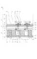
次に、図1を用いて本実施例の固体撮像装置を説明する。図1は、図11の固体撮像装置300に対応した固体撮像装置100の断面図である。図1は、図11の光電変換素子303、転送トランジスタ304、増幅トランジスタ306に対応する、2画素分の断面図であり、その他の部分については記載を省略する。 Next, the solid-state imaging device of the present embodiment will be described with reference to FIG. FIG. 1 is a cross-sectional view of a solid-
図1において、第1のチップ101と、第2のチップ102と、第1のチップと第2のチップとの接合面103とが示されている。第1のチップ101は図11の第1のチップ308と、第2のチップ102は図11の第2のチップ309と対応している。 In FIG. 1, a
第1のチップ101は第1の基板104を有する。第1の基板104において、トランジスタが形成される面を主面105とし、その反対の面を裏面106とする。第1の基板104には、図11における光電変換素子303、転送トランジスタ304を構成する各部位が配されている。そして、第1のチップ101の第1の基板104の主面105側の上部には、アルミニウムを主成分とした配線(アルミニウム配線)からなる第1の配線層122と第2の配線層123とを含む多層配線構造107を有する。ここで、第1の配線層122の配線と第2の配線層123の配線との接続や、ゲート電極と第1の配線層の配線との接続などは、例えばタングステンからなるプラグによって接続されている。 The
第2のチップ102は第2の基板108を有する。第2の基板108において、トランジスタが形成される面を主面109とし、その反対の面を裏面110とする。第2の基板108の主面109の上部には、銅を主成分とした配線(銅配線)の第1の配線層128と、アルミニウム配線の第2の配線層129とを含む多層配線構造111が形成されている。第1の配線層128はシングルダマシン構造であり、その上部に銅のための拡散防止膜131を有している。拡散防止膜131は、第1の配線層128の上部と第1の配線層128の上面と同一面を形成する絶縁膜を覆っている。この拡散防止膜は、例えば、シリコンナイトライドやシリコンカーバイドである。
ゲート電極などと第1の配線層128の配線と、第1の配線層128と第2の配線層129との接続は、例えばタングステンからなるプラグによってなされている。そして、第2の基板108には、図11の増幅トランジスタ306を構成する各部位が配されている。なお、説明において、各チップにおいて、基板の主面から裏面に向かう方向を下方向もしくは深い方向とし、裏面から主面に向かう方向を上方向もしくは浅い方向とする。The
The gate electrode and the wiring of the
ここで、本実施例の固体撮像装置においては、第1のチップ101と第2のチップ102のそれぞれの基板の主面105および主面109とが対向して積層されている。図1では、第1のチップ101と第2のチップ102の接続部の構成は、第1のチップ101のフローティングディフュージョン領域(以下、FD領域)113と第2のチップ102の増幅トランジスタのゲート電極126との接続のみ示している。具体的には、第1のチップ101のFD領域113は多層配線構造107、接続部311、多層配線構造111を介して、増幅トランジスタのゲート電極126と接続している。なお、転送トランジスタのゲート電極114への制御信号を供給する図11に示す接続部310は図1においては不図示である。そして、本実施例の固体撮像装置においては、第1の基板104の裏面106側から光が入射する裏面入射型の固体撮像装置である。 Here, in the solid-state imaging device according to the present embodiment, the
各チップについて詳細に説明する。まず、第1のチップ101の第1の基板104には、ウエル115と、光電変換素子を形成するN型の電荷蓄積領域112と、転送トランジスタのゲート電極114とが配されている。更に、第1の基板104には、転送トランジスタのドレイン領域113と、素子分離領域117と、P型の半導体領域116とが配されている。ウエル115は、トランジスタや光電変換素子が配される半導体領域であり、ここではN型でもP型でもどちらでもよい。P型の半導体領域116は、第1の基板104の裏面106のシリコンとシリコン酸化膜界面にて生じる暗電流の抑制が可能であり、また光電変換素子の一部としても機能可能である。電荷蓄積領域112は、光電変換素子にて生じた電荷(電子)を蓄積し、図1では転送ゲート側にP型の保護層を有している。素子分離領域117は、P型の半導体領域からなり、図示していないがLOCOS分離やSTI分離といった絶縁膜を含む素子分離構造を有していてもよい。転送トランジスタのドレイン領域113は図11におけるノード305を構成し、FD領域と称される。そして、第1のチップ101は、第1の基板104の裏面106側に、反射防止膜118、遮光膜119、平坦化層などを含むカラーフィルタ層120、マイクロレンズ121を有する。 Each chip will be described in detail. First, on the
次に、第2のチップ102の第2の基板108には、ウエル124と、図11における増幅トランジスタ306を構成するソース領域およびドレイン領域125と、同増幅トランジスタのゲート電極126と、素子分離領域127と、が配されている。トランジスタのゲート電極126とソース領域およびドレイン領域125とに高融点金属化合物層136が配されている。ウエル124はP型の半導体領域である。高融点金属化合物層は、コバルトやチタンといった高融点金属とシリコン半導体基板との化合物である。ここで、本実施例の固体撮像装置の第2のチップ102のみが多層配線構造に銅配線を含む。また、図11に示す周辺回路部302を構成する領域の上部にも銅配線を含む多層配線構造が配される(不図示)。 Next, on the
このような第2の基板に配された制御回路のトランジスタのための多層配線構造が銅配線を含むことによって、配線間隔の微細化が可能となる。また、このような銅配線を有する多層配線構造を第2のチップ102にのみ有することで、光電変換素子への銅の混入を低減することが可能となり、銅の混入によって生じるノイズを低減することが可能となる。 Since the multilayer wiring structure for the transistor of the control circuit arranged on the second substrate includes the copper wiring, the wiring interval can be miniaturized. In addition, since the multilayer wiring structure having such a copper wiring is included only in the
また、拡散防止膜131を有することで、第2のチップに配された銅配線の銅が第1のチップの光電変換素子やFD領域を構成する半導体領域に混入することをより抑制することが可能となる。 In addition, by including the
なお、本実施例において、第2チップの第2の配線層129をアルミニウム配線としたのは、接続部を構成するために、第2の配線層129の配線を形成する導電体が露出している必要があるためである。ここで、第2の配線層129は露出した導電体から銅が拡散する可能性があるため、アルミニウム配線にすると良い。 In the present embodiment, the
また、銅のための拡散防止膜131が高融点金属の拡散防止膜としても機能可能である。よって、高融点金属が光電変換素子を構成する半導体領域へ混入することを低減することが可能となり、高融点金属の混入によって生じるノイズを低減することが可能となる。 Further, the
また、本実施例の変形例として、増幅トランジスタが第1の基板に配されていてもよく、少なくとも、本実施例のように光電変換素子に加えてFD領域を第1の基板104に配することが好ましい。それは、光電変換素子で生じた信号電荷が保持される光電変換素子やFD領域を構成する半導体領域への銅の拡散を低減させることが可能であるためである。 As a modification of the present embodiment, the amplification transistor may be disposed on the first substrate, and at least the FD region is disposed on the
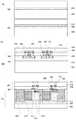
本実施例の固体撮像装置を図2を用いて説明する。本実施例の固体撮像装置は、実施例1の固体撮像装置とは、図11に示すような回路は等しく、チップの積層構造が異なる。以下、回路については説明を省略し、図2に示す構成について説明を行う。 The solid-state imaging device of the present embodiment will be described with reference to FIG. The solid-state imaging device according to the present embodiment is the same as the solid-state imaging device according to the first embodiment in the circuit as shown in FIG. Hereinafter, description of the circuit will be omitted, and the configuration shown in FIG. 2 will be described.
図2は、図11の回路に対応した固体撮像装置200の断面図である。図2は、図11の光電変換素子303、転送トランジスタ304、増幅トランジスタ306に対応する、2画素分の断面図であり、その他の部分については記載を省略する。 FIG. 2 is a cross-sectional view of the solid-
図2には、第1のチップ201と、第2のチップ202と、第1のチップと第2のチップとの接合面203とが示されている。第1のチップ201は図11の第1のチップ308と、第2のチップ202は図11の第2のチップ309と対応している。 FIG. 2 shows a
第1のチップ201は第1の基板204を有する。第1の基板204において、トランジスタが配される面を主面205とし、その反対の面を裏面206とする。第1の基板204には、図11における光電変換素子303、転送トランジスタ304が配されている。そして、第1の基板204の主面205の上部には、アルミニウム配線からなる第1の配線層222と第2の配線層223とを含む多層配線構造207が配されている。また、多層配線構造207は、実施例1と同様に、タングステンのプラグを有する。 The
第2のチップ202は第2の基板208を有する。第2の基板208において、トランジスタが形成される面を主面209とし、その反対の面を裏面210とする。第2の基板208の主面209の上部には、銅配線からなる第1の配線層228と第2の配線層229とを含む多層配線構造211が配されている。本実施例では実施例1と異なり第2の配線層も銅配線である。第1の配線層228はシングルダマシン構造であり、第2の配線層229はデュアルダマシン構造であり、それぞれ銅に対する拡散防止膜231、232が上部に配される。拡散防止膜231、232は、例えば、シリコンナイトライドやシリコンカーバイドからなる膜である。また、ゲート電極などと第1の配線層228との接続は、例えばタングステンのプラグによってなされている。そして、第2の基板208には、図11における増幅トランジスタ306を構成する各部位が配されている。 The
ここで、本実施例の固体撮像装置においては、第1の基板204の主面205と第2の基板208の裏面210とが対向して積層されている。図2では、第1のチップ201と第2のチップ202の接続部の構成は、第1のチップ201のFD領域213と第2のチップ202の増幅トランジスタのゲート電極226との接続のみ示している。具体的には、第1のチップ201のFD領域213は多層配線構造207、接続部311、多層配線構造211を介して、増幅トランジスタのゲート電極226と接続している。ここで、接続部311の一部を構成する、第2の基板208を関する貫通電極235が配されている。この貫通電極によって、FD領域213と増幅トランジスタのゲート電極226とが接続される。なお、転送トランジスタのゲート電極214への制御信号を供給する図11における接続部310は不図示である。そして、本実施例の固体撮像装置においては、第1の基板204の裏面206側から光が入射する裏面入射型の固体撮像装置である。 Here, in the solid-state imaging device of the present embodiment, the
次に、各チップについて詳細に説明する。第1のチップ201の第1の基板204には、ウエル215と、光電変換素子を形成するN型の電荷蓄積領域212と、転送トランジスタのゲート電極214とが配されている。更に、第1の基板204には転送トランジスタのドレイン領域213と、素子分離領域217と、P型の半導体領域216とが配されている。そして、第1のチップ201は、第1の基板204の裏面206側に、反射防止膜218、遮光膜219、平坦化層などを含むカラーフィルタ層220、マイクロレンズ221を有する。 Next, each chip will be described in detail. On the
次に、第2のチップ202の第2の基板208には、ウエル224と、素子分離領域227と、が配されている。更に、第2の基板208には図11における増幅トランジスタ306の各部位であるソース領域およびドレイン領域225とゲート電極226とが配されている。トランジスタのゲート電極226とソース領域およびドレイン領域225には高融点金属化合物層236が配されている。更に、第2の基板208の上部に第1の配線層228、第2の配線層229を有し、第2の基板208の最深部に絶縁層234を有する。更に、第2のチップ202の上部に接着層233と支持基板234とを有している。実施例2における絶縁層、接着層233、支持基板234については後述する。 Next, a well 224 and an
ここで、本実施例の固体撮像装置の第2のチップ202に配された多層配線構造は、銅配線を含む。第2の基板に配された多層配線構造が銅配線によって構成されることで、配線の微細化が可能となる。また、このような銅配線を第2のチップ202にのみ有することで、光電変換素子への銅の混入を低減することが可能となり、銅の混入によって生じるノイズを低減することが可能となる。 Here, the multilayer wiring structure disposed on the
また、銅のための拡散防止膜231、232を有することで、第2のチップに配された銅配線の銅が第1のチップの光電変換素子やFD領域を構成する半導体領域に混入することを抑制することが可能となる。なお、第2の拡散防止膜232は平坦な上面を保っている事が好ましい。それは、第2の拡散防止膜232の上面が接着層233との接着面となっているためである。 Further, by having the
本実施例の固体撮像装置を図3を用いて説明する。本実施例の固体撮像装置は、実施例1の固体撮像装置100に対応し、実施例1の固体撮像装置100に対して拡散防止膜の形態が異なる。以下、図3に示す構成について説明を行う。なお、実施例1と等しい構成については説明を省略する。 The solid-state imaging device of the present embodiment will be described with reference to FIG. The solid-state imaging device of the present embodiment corresponds to the solid-
図3の固体撮像装置400においても、銅のための拡散防止膜131が第1の配線層の銅配線を覆っている。ここで、拡散防止膜131が各配線のパターンに対応して、パターニングされている。拡散防止膜131の材料は図1と同様である。図1の構成に比べて、図3のようなパターニングされた拡散防止膜131を有することで、さらに配線間および配線層間のカップリング容量を低減することが可能となる。カップリング容量を低減することで、配線間における信号の混入や配線における信号遅延を抑制することが可能となる。 Also in the solid-
次に、図3に示した固体撮像装置400の製造方法を図5および図6を用いて説明する。まず、図5(a)では第1の基板104となるフォトダイオード形成部材(以下PD形成部材)501と第2の基板108となる回路形成部材502とを準備する。PD形成部材501は、P型半導体領域116と絶縁層503とを含む。このPD形成部材501は、SOI基板を使用しており、P型半導体領域116はイオン注入でもエピタキシャル成長によって形成されていてもよい。 Next, a method for manufacturing the solid-
次に、図5(b)に示すように、PD形成部材501に、電荷蓄積部112や転送ゲート電極114等の素子を形成する。このPD形成部材501の転送ゲート電極が配された面が、後の第1の基板104の主面105となる。次に、PD形成部材501の上部に多層配線構造107を形成する。まず、電荷蓄積部112や転送ゲート電極114を覆うシリコン酸化膜からなる第1の層間絶縁膜512を形成する。その後、第1の層間絶縁膜512の任意の箇所にタングステンからなるプラグ511を形成する。プラグ511は、次のように形成する。まず、第1の層間絶縁膜512にコンタクトホールを形成したのち、コンタクトホールを埋めるようにバリアメタル膜とタングステン膜を形成する。そして、不要な部分のバリアメタル膜とタングステン膜をエッチングやCMPなどの技術を用いて除去し、プラグ511が形成される。プラグ511が形成された後、第1の層間絶縁膜512とプラグ511上に、第1の配線層122となるアルミニウム配線を形成する。第1の配線層122は、バリアメタル膜とアルミニウム膜とを積層して形成したのち、それらを所望のパターンにエッチングなどでパターニングすることによって形成される。第1の配線層122が形成された後、第1の層間絶縁膜512と第1の配線層122とを覆うシリコン酸化膜からなる第2の層間絶縁膜513を形成する。次に、第2の層間絶縁膜513中にタングステンからなるプラグ514を形成する。プラグ514の形成方法は、プラグ511と同様である。そして、任意の箇所に、第2の配線層123となるアルミニウム配線を、第1の配線層122と同様の方法で形成する。そして、第2の配線層123を覆うシリコン酸化膜からなる第3の層間絶縁膜515を形成し、第3の層間絶縁膜515をエッチングやCMPによって平坦化する。この平坦化工程によって、第2の配線層123の上部を覆う第3の層間絶縁膜515を除去し、第2の配線層123の上面を露出させる。ここで、第2の配線層123の上面と第3の層間絶縁膜515の上面とが同一面を有する。このようにして、多層配線構造107が構成される。 Next, as shown in FIG. 5B, elements such as the
また、図5(b)において、回路形成部材502には、ウエル124を形成し、増幅トランジスタを含むトランジスタ等の回路を形成する。そして、回路形成部材502の上部に多層配線構造111を形成する。まず、トランジスタのソース領域およびドレイン領域125やゲート電極126などを覆う、シリコン酸化膜からなる第1の層間絶縁膜506を形成する。その後、第1の層間絶縁膜506の任意の箇所にタングステンからなるプラグ505を形成する。プラグ505の形成方法は、プラグ509と同様である。次に、第1の層間絶縁膜506とプラグ505とを覆う、シリコン酸化膜からなる第2の層間絶縁膜507を形成する。ここで、第2の層間絶縁膜507はシリコンナイトライドや有機系絶縁膜でもよく、これらの膜とシリコン酸化膜との積層膜であってもよい。この第2の層間絶縁膜507の任意の箇所に第1の配線層128となる溝(トレンチ)を形成する。次に、溝を埋めるようにバリアメタル膜と銅の膜を積層して形成した後、不要な部分のバリアメタル膜と銅の膜をCMPによって除去し、平坦化する。その後、第2の層間絶縁膜507と溝に配されたバリアメタルと銅を覆う、銅のための拡散防止膜となる例えばシリコンナイトライドの膜を形成する。シリコンナイトライドの膜の底面が溝の表面、つまり、銅配線のパターンの表面全体を覆うように、シリコンナイトライドの膜をパターニングし、銅のための拡散防止膜131が形成される。次に、第2の層間絶縁膜507と拡散防止膜131とを覆う、例えばシリコン酸化膜からなる第3の層間絶縁膜508を形成する。そして、この第3の層間絶縁膜508の任意の箇所に第1の配線層と第2の配線層とを接続するためのタングステンからなるプラグ510を形成する。そして、アルミニウム配線からなる第2の配線層129を形成し、第2の配線層129を覆う、シリコン酸化膜からなる第4の層間絶縁膜509を形成する。そして、接続部のために第4の層間絶縁膜509を第2の配線層129の上面が露出するようにエッチングやCMPによって除去する。第2の配線層129の上面と第4の層間絶縁膜509の上面とが同一の面を構成する。このようにして、多層配線構造111が構成される。 In FIG. 5B, a well 124 is formed in the
次に、図6(c)において、回路形成部材502の上下を反転させ、後の第2の基板の主面109と後の第1の基板の主面105とを対向させて配置し、例えば、マイクロバンプを設けて接合する。 Next, in FIG. 6C, the
最後に、図6(d)に示すように、PD形成部材501の不要部分504および絶縁層503をCMPやエッチングなどによって除去し、PD形成部材501の薄膜化をはかり、第1基板104を形成する。その後、第1の基板104の裏面106の上部にシリコンナイトライドなどからなる反射防止膜118を形成する。反射防止膜118の形成後に、反射防止膜118の上部に、タングステン膜を形成しパターニングをすることで、遮光膜119を形成する。その後、平坦化層やカラーフィルタ層120を形成し、マイクロレンズ121を形成する。このような製造方法によって、図3に示した固体撮像装置400を製造することが可能である。 Finally, as shown in FIG. 6D,
本実施例の固体撮像装置によれば、実施例1に比べて信号の読み出し動作の高速化および配線のカップリング低減が可能となる。 According to the solid-state imaging device of the present embodiment, it is possible to increase the speed of the signal readout operation and reduce the coupling of the wiring as compared with the first embodiment.
本実施例の固体撮像装置を図4を用いて説明する。本実施例の固体撮像装置は、実施例2の固体撮像装置200に対応する構成であり、実施例2の固体撮像装置に比べて拡散防止膜を有する点が異なる。以下、図4に示す構成について説明を行う。なお、実施例2など他の実施例と等しい構成については説明を省略する。 The solid-state imaging device of the present embodiment will be described with reference to FIG. The solid-state imaging device according to the present embodiment has a configuration corresponding to the solid-
図4の固体撮像装置500においても、実施例3と同様に、銅のための第1の拡散防止膜231と第2の拡散防止膜232が、各配線層の配線のパターンに対応してパターニングされている。拡散防止膜231、232の材料は図3と同様である。このようにパターニングされた拡散防止膜231、232を有することで、更に、配線間および配線層間のカップリング容量を低減することが可能となる。カップリング容量を低減することで、配線間における信号の混入や配線における信号遅延を抑制することが可能となる。 Also in the solid-
次に、図4に示した固体撮像装置500の製造方法を図7から図9を用いて説明する。まず、図7(a)において、第1の基板204となるフォトダイオード形成基板(以下、PD形成部材)701と、第2の基板208となる回路形成部材702とを準備する。PD形成部材701は、P型半導体領域216と絶縁層703とが配されている。PD形成部材701は、SOI基板を使用しており、P型半導体領域216はイオン注入でもエピタキシャル成長によって形成されていてもよい。回路形成部材702は、絶縁層234が配されている。回路形成部材702は、SOI基板を使用している。 Next, a method for manufacturing the solid-
次に、図7(b)のPD形成部材701において、ウエル215や電荷蓄積部212や転送ゲート電極214等の素子を形成する。このPD形成部材701の転送ゲート電極が配された面が、後の第1の基板204の主面205となる。そして、PD形成部材701の上部に多層配線構造207を形成する。多層配線構造207は、アルミニウム配線の第1および第2の配線層の他に、第1の層間絶縁膜709と、プラグ710と、第2の層間絶縁膜511と、プラグ712と、第3の層間絶縁膜713を含む。多層配線構造の形成方法については、実施例3と同様である。 Next, in the
また、図7(b)において、回路形成部材702には、ウエル224を形成し、増幅トランジスタを含むトランジスタ等の回路を形成する。そして、回路形成部材702の上部には多層配線構造211を形成する。図7(b)において多層配線構造211は、第1の層間絶縁膜706、プラグ707、第2の層間絶縁膜708、銅配線からなる第1の配線層228、第1の拡散防止膜231、第3の層間絶縁膜709を有する。これらの形成方法については、実施例3の各配線層やプラグと同様に形成可能であり、説明を省略する。 In FIG. 7B, a well 224 is formed in the
次に、図8(c)において、回路形成部材702の第3の層間絶縁膜709の上部に、接着層714と支持基板715とを形成する。そして、回路形成部材702の不要部分704をエッチングやCMPなどで除去し、後の第2の基板208の裏面210を露出させる。その後、第2の基板208の裏面210と第1の基板204の表面205とが対向するように、回路形成部材702とPD形成部材701とを貼り合わせる。そして、接着層714と支持基板715を除去する。 Next, in FIG. 8C, an
次に、図8(d)において、第1の基板204との導通を取るための貫通電極235を形成する。この貫通電極235の製造方法については、一般の半導体プロセスが利用できる。そして、第3の層間絶縁膜709の任意の箇所に第1の配線層と第2の配線層とを接続するためのプラグと、第2の配線層229のための溝を形成する。溝を形成した後は、第1の配線層228の形成方法と同様である。このプラグおよび第2の配線層229の形成方法はいわゆるデュアルダマシンプロセスである。デュアルダマシン構造の銅配線からなる第2の配線層229を形成したのち、第2の拡散防止膜232を形成する。第2の拡散防止膜232も第1の拡散防止膜231と同様に、シリコンナイトライド等の膜を第2の配線層229上に形成した後、第2の配線層229の配線のそれぞれを覆うようにパターニングされ、第2の拡散防止膜232が形成される。第2の拡散防止膜232を覆う、例えばシリコン酸化膜からなる第4の層間絶縁膜716を形成し、平坦化処理を行う。第4の層間絶縁膜716は保護膜を兼ねるシリコンナイトライドの膜などであってもよい。 Next, in FIG. 8D, a through
次に、図9(e)において、第4の層間絶縁膜716の上部に接着層233と支持基板234を設ける。そして、PD形成部材701の不要部分705をエッチングやCMPなどによって除去し、第1の基板204が形成される。その後、第1の基板204の裏面206の上部に例えばシリコンナイトライドからなる反射防止膜218を形成する。その後、反射防止膜218の上部に例えばタングステンからなる遮光膜219を形成する。更に、遮光膜219の上部に平坦化層やカラーフィルタ層120を形成し、マイクロレンズ121を形成する。以上の製造方法によって、図4に示す固体撮像装置500が形成できる。 Next, in FIG. 9E, an
本実施例の固体撮像装置によれば、実施例2に比べて信号の読み出し動作の高速化および配線のカップリング低減が可能となる。 According to the solid-state imaging device of the present embodiment, it is possible to speed up the signal reading operation and reduce the coupling of the wiring as compared with the second embodiment.
本実施例の固体撮像装置を図10を用いて説明する。図10に示す本実施例の固体撮像装置600は実施例3の固体撮像装置400に対応する構成であり、固体撮像装置700は実施例4の固体撮像装置500に対応する構成である。本実施例では、銅のための拡散防止膜を更に第1のチップが有する構成が特徴である。以下、実施例3あるいは実施例4と等しい構成については説明を省略する。 A solid-state imaging device according to this embodiment will be described with reference to FIG. A solid-
図10(a)に示す固体撮像装置600においては、固体撮像装置400に加えて第3の拡散防止膜801が第1のチップ101の多層配線構造107に設けられている。具体的には、第2の配線層123の上面と第3の拡散防止膜801の上面とで同一面を形成し、第1の基板104の全面を覆うように配されている。この拡散防止膜801を有することで、第2のチップ102からの銅の拡散をより低減することが可能となる。更に、図10(a)では、第1の配線層128に加えて第2の配線層129も銅配線からなる。具体的には、第2の配線層129は、第1の配線層128と第2の配線層129とを接続するためのプラグと第2の配線層129とが一体となったデュアルダマシン構造である。このような場合においても、接続部311において露出した第2の配線層129の銅の拡散を抑制することが可能となる。 In the solid-
なお、この第3の拡散防止膜801は多層配線構造107に含まれていれば、どの位置に配されていても同一の効果を有する。また、第3の拡散防止膜801は、第1の基板104の全面を覆っていなくても銅の拡散の効果は有するが、第1の基板の全面を覆っていることが好ましい。そして、第3の拡散防止膜801は、第2の基板108上に高融点金属化合物層136が配されている場合に、高融点金属のための拡散防止膜としても機能することが可能である。 Note that the third
次に、図10(b)に示す固体撮像装置700においては、固体撮像装置500に加えて、第3の拡散防止膜901が、第1のチップ201の多層配線構造207に設けられている。具体的には、第2の配線層223を覆って第3の拡散防止膜901が設けられている。このような構成にすることで、銅が第2の基板208の内部を拡散してきた場合においても、第1の基板204の光電変換素子等への銅の拡散を抑制することが可能となる。 Next, in the solid-
なお、第3の拡散防止膜901は、多層配線構造207のどこに配置されていてもよいが、第2の配線層223の上部に配されている構成は配線層間のカップリング容量を低減することが出来るため好ましい。また、第2の基板208上に高融点金属化合物層136が配されている場合には、高融点金属が第2の基板208の内部を拡散してきた場合においても、第3の拡散防止膜901によって第1の基板204の光電変換素子等への高融点金属の拡散を抑制することが可能となる。 The third
本実施例では、本発明の光電変換装置を撮像装置として撮像システムに適用した場合について詳述する。撮像システムとして、デジタルスチルカメラやデジタルカムコーダーなどがあげられる。図12に、撮像システムの例としてデジタルスチルカメラに光電変換装置を適用した場合のブロック図を示す。 In this embodiment, a case where the photoelectric conversion device of the present invention is applied to an imaging system as an imaging device will be described in detail. Examples of the imaging system include a digital still camera and a digital camcorder. FIG. 12 shows a block diagram when a photoelectric conversion device is applied to a digital still camera as an example of an imaging system.
図12において、1はレンズの保護のためのバリア、2は被写体の光学像を撮像装置4に結像させるレンズ、3はレンズ2を通った光量を可変するための絞りである。4は上述の各実施例で説明した固体撮像装置である撮像装置である。撮像装置4は、レンズ2により結像された光学像を画像データとして変換する。ここで、撮像装置4にはAD変換器が配され、具体的には第2のチップにAD変換器が形成されている。7は撮像装置4より出力された撮像データに各種の補正やデータを圧縮する信号処理部である。そして、図12において、8は撮像装置4および信号処理部7に、各種タイミング信号を出力するタイミング発生部、9は各種演算とデジタルスチルカメラ全体を制御する全体制御・演算部である。10は画像データを一時的に記憶する為のメモリ部、11は記録媒体に記録または読み出しを行うためのインターフェース部、12は撮像データの記録または読み出しを行う為の半導体メモリ等の着脱可能な記録媒体である。そして、13は外部コンピュータ等と通信する為のインターフェース部である。ここで、タイミング信号などは撮像システムの外部から入力されてもよく、撮像システムは少なくとも撮像装置4と、撮像装置から出力された撮像信号を処理する信号処理部7とを有すればよい。本実施例では、撮像装置4にAD変換器が設けられている場合を説明したが、撮像装置とAD変換器とが別のチップであってもよい。また、撮像装置4に信号処理部7などが設けられていてよい。 In FIG. 12, 1 is a barrier for protecting the lens, 2 is a lens for forming an optical image of a subject on the
以上のように、本発明の光電変換装置を撮像システムに適用することが可能である。本発明の光電変換装置を撮像システムに適用することにより、高品質な画像の取得が可能となる。 As described above, the photoelectric conversion device of the present invention can be applied to an imaging system. By applying the photoelectric conversion device of the present invention to an imaging system, it is possible to acquire a high-quality image.
以上述べてきたように、本発明の固体撮像装置によって、微細化が可能で、光電変換素子での暗電流を低減することが可能となる。各実施例は説明した構成に限定されず、また各実施例は適宜組み合わせ可能である。 As described above, the solid-state imaging device of the present invention can be miniaturized and can reduce the dark current in the photoelectric conversion element. Each embodiment is not limited to the configuration described, and each embodiment can be appropriately combined.
本発明は、デジタルスチルカメラやデジタルカムコーダーなどの撮像システムに用いられる固体撮像装置に適用可能である。 The present invention can be applied to a solid-state imaging device used in an imaging system such as a digital still camera or a digital camcorder.
101 第1のチップ
102 第2のチップ
103 接合面
104 第1の基板
107 多層配線構造
108 第2の基板
111 多層配線構造
112 光電変換素子
124 ウエル
125 増幅トランジスタのソース・ドレイン領域
126 増幅トランジスタのゲート電極
131 拡散防止膜
Claims (11)
Translated fromJapanese前記光電変換素子にて生じた電荷に基づく信号を読み出すための回路を含む周辺回路部を主面側に有する第2の基板とを積層した固体撮像装置において、
前記第1の基板の主面側に配された、アルミニウム配線からなる多層配線構造と、
前記第2の基板の主面側に配された、銅配線からなる多層配線構造と、を有する固体撮像装置。A first substrate having a photoelectric conversion element and a transfer gate electrode for transferring charges from the photoelectric conversion elementon a main surface side ;
In a solid-state imaging device in which a second substrate having a peripheral circuit portion including a circuit for reading out a signal based on a charge generated in the photoelectric conversion element is disposed on themain surface side ,
A multilayer wiring structure made of aluminum wiring, disposedon themain surface side of the first substrate;
A solid-state imaging device having a multilayer wiring structure made of copper wiringand disposed on amain surface side of the second substrate.
前記銅のための拡散防止膜は、前記高融点金属の拡散防止膜としても機能することを特徴とする請求項4に記載の固体撮像装置。In the peripheral circuit portion disposed on the second substrate, a refractory metal compound layer is disposed,
The solid-state imaging device according to claim 4, wherein the diffusion preventing film for copper also functions as a diffusion preventing film for the refractory metal.
前記第2の基板に、前記フローティングディフュージョン領域の電位に基づく信号が入力されるゲート電極を有する増幅トランジスタと、前記増幅トランジスタのゲート電極をリセット電位に設定するためのリセットトランジスタとが配され、前記第2の基板の上部には前記増幅トランジスタのゲート電極に基づく信号が出力される信号線が配されることを特徴とする請求項1乃至8のいずれか1項に記載の固体撮像装置。On the first substrate, the floating diffusion region in which the charge from the photoelectric conversion element by the transfer gate electrode is transferredis disposed,
An amplification transistor having a gate electrode to which a signal based on the potential of the floating diffusion region is input and a reset transistor for setting the gate electrode of the amplification transistor to a reset potential are disposed on the second substrate, 9. The solid-state imaging device according to claim 1, wherein a signal linefor outputting a signal based on a gate electrode of the amplification transistor is disposed on the second substrate. 10.
前記第2の基板の主面側の銅配線からなる多層配線構造に、前記増幅トランジスタのゲート電極に基づく信号が出力される信号線が配されることを特徴とする請求項1乃至8のいずれか1項に記載の固体撮像装置。An amplification transistor having a floating diffusion region to which the charge from the photoelectric conversion element is transferred by the transfer gate electrode to the first substrate, and a gate electrode to which a signal based on a potential of the floating diffusion region is input; A reset transistor for setting the gate electrode of the amplification transistor to a reset potential,
9. The signal line for outputting a signal based on the gate electrode of the amplification transistor is arranged in amultilayer wiring structure madeof copper wiring on themain surface side of the second substrate. The solid-state imaging device according to claim 1.
前記固体撮像装置から出力される信号を処理する信号処理部とを有する撮像システム。A solid-state imaging device according to any one of claims 1 to 10,
An imaging system comprising: a signal processing unit that processes a signal output from the solid-state imaging device.
Priority Applications (6)
| Application Number | Priority Date | Filing Date | Title |
|---|---|---|---|
| JP2009296522AJP5489705B2 (en) | 2009-12-26 | 2009-12-26 | Solid-state imaging device and imaging system |
| US13/517,357US8912578B2 (en) | 2009-12-26 | 2010-12-22 | Solid-state image pickup device and image pickup system |
| CN201080058034.6ACN102714212B (en) | 2009-12-26 | 2010-12-22 | Solid-state image pickup device and image pickup system |
| PCT/JP2010/007414WO2011077709A1 (en) | 2009-12-26 | 2010-12-22 | Solid-state image pickup device and image pickup system |
| EP10807492.3AEP2517248B1 (en) | 2009-12-26 | 2010-12-22 | Solid-state image pickup device and image pickup system |
| US14/543,237US9385152B2 (en) | 2009-12-26 | 2014-11-17 | Solid-state image pickup device and image pickup system |
Applications Claiming Priority (1)
| Application Number | Priority Date | Filing Date | Title |
|---|---|---|---|
| JP2009296522AJP5489705B2 (en) | 2009-12-26 | 2009-12-26 | Solid-state imaging device and imaging system |
Publications (3)
| Publication Number | Publication Date |
|---|---|
| JP2011138841A JP2011138841A (en) | 2011-07-14 |
| JP2011138841A5 JP2011138841A5 (en) | 2013-02-21 |
| JP5489705B2true JP5489705B2 (en) | 2014-05-14 |
Family
ID=43650059
Family Applications (1)
| Application Number | Title | Priority Date | Filing Date |
|---|---|---|---|
| JP2009296522AActiveJP5489705B2 (en) | 2009-12-26 | 2009-12-26 | Solid-state imaging device and imaging system |
Country Status (5)
| Country | Link |
|---|---|
| US (2) | US8912578B2 (en) |
| EP (1) | EP2517248B1 (en) |
| JP (1) | JP5489705B2 (en) |
| CN (1) | CN102714212B (en) |
| WO (1) | WO2011077709A1 (en) |
Cited By (1)
| Publication number | Priority date | Publication date | Assignee | Title |
|---|---|---|---|---|
| US10608034B2 (en) | 2009-12-26 | 2020-03-31 | Canon Kabushiki Kaisha | Solid-state image pickup apparatus and image pickup system |
Families Citing this family (40)
| Publication number | Priority date | Publication date | Assignee | Title |
|---|---|---|---|---|
| JP2011009645A (en)* | 2009-06-29 | 2011-01-13 | Toshiba Corp | Semiconductor device and method of manufacturing the same |
| JP2012015274A (en)* | 2010-06-30 | 2012-01-19 | Canon Inc | Solid-state imaging apparatus, and method of manufacturing the same |
| JP2012124318A (en)* | 2010-12-08 | 2012-06-28 | Sony Corp | Method of manufacturing solid state imaging device, solid state image sensor, and electronic apparatus |
| CN103022062B (en)* | 2011-07-19 | 2016-12-21 | 索尼公司 | Solid-state imaging device, manufacturing method thereof, and electronic device |
| JP2013077711A (en) | 2011-09-30 | 2013-04-25 | Sony Corp | Semiconductor device and manufacturing method of semiconductor device |
| JP5981711B2 (en)* | 2011-12-16 | 2016-08-31 | ルネサスエレクトロニクス株式会社 | Semiconductor device and manufacturing method of semiconductor device |
| JP5970826B2 (en)* | 2012-01-18 | 2016-08-17 | ソニー株式会社 | SEMICONDUCTOR DEVICE, SEMICONDUCTOR DEVICE MANUFACTURING METHOD, SOLID-STATE IMAGING DEVICE, AND ELECTRONIC DEVICE |
| JP6128787B2 (en) | 2012-09-28 | 2017-05-17 | キヤノン株式会社 | Semiconductor device |
| JP2014099582A (en) | 2012-10-18 | 2014-05-29 | Sony Corp | Solid-state imaging device |
| KR102517997B1 (en)* | 2013-01-16 | 2023-04-06 | 소니 세미컨덕터 솔루션즈 가부시키가이샤 | Solid-state imaging element and electronic device |
| JP2014199898A (en) | 2013-03-11 | 2014-10-23 | ソニー株式会社 | Solid-state imaging element and method of manufacturing the same, and electronic equipment |
| JP2015041677A (en)* | 2013-08-21 | 2015-03-02 | ルネサスエレクトロニクス株式会社 | Semiconductor device and manufacturing method of the same |
| JP6217458B2 (en)* | 2014-03-03 | 2017-10-25 | ソニー株式会社 | SEMICONDUCTOR DEVICE, ITS MANUFACTURING METHOD, AND ELECTRONIC DEVICE |
| JP6215246B2 (en)* | 2014-05-16 | 2017-10-18 | ソニーセミコンダクタソリューションズ株式会社 | Solid-state imaging device, manufacturing method of solid-state imaging device, and electronic apparatus |
| JP2016151523A (en)* | 2015-02-18 | 2016-08-22 | 浜松ホトニクス株式会社 | Infrared detection device |
| US12087629B2 (en)* | 2015-05-18 | 2024-09-10 | Adeia Semiconductor Technologies Llc | Through-dielectric-vias (TDVs) for 3D integrated circuits in silicon |
| US9978791B2 (en)* | 2015-07-31 | 2018-05-22 | Taiwan Semiconductor Manufacturing Co., Ltd | Image sensor and method for manufacturing the same |
| JP2017204510A (en)* | 2016-05-09 | 2017-11-16 | キヤノン株式会社 | Method for manufacturing photoelectric conversion device |
| EP3493275B1 (en)* | 2016-07-27 | 2022-03-23 | Hamamatsu Photonics K.K. | Light detection device |
| FR3059143B1 (en) | 2016-11-24 | 2019-05-31 | Stmicroelectronics (Crolles 2) Sas | IMAGE SENSOR CHIP |
| US10431614B2 (en) | 2017-02-01 | 2019-10-01 | Semiconductor Components Industries, Llc | Edge seals for semiconductor packages |
| US9929203B1 (en)* | 2017-04-27 | 2018-03-27 | Taiwan Semiconductor Manufacturing Co., Ltd. | Semiconductor device and method for fabricating thereof |
| JP7038494B2 (en)* | 2017-06-15 | 2022-03-18 | ルネサスエレクトロニクス株式会社 | Solid-state image sensor |
| US10825854B2 (en)* | 2017-08-16 | 2020-11-03 | Facebook Technologies, Llc | Stacked photo sensor assembly with pixel level interconnect |
| US10522580B2 (en) | 2017-08-23 | 2019-12-31 | Taiwan Semiconductor Manufacturing Co., Ltd. | Structure and formation method of light-sensing device |
| JP2017216480A (en)* | 2017-09-01 | 2017-12-07 | ルネサスエレクトロニクス株式会社 | Semiconductor device and manufacturing method of the same |
| JP7175905B2 (en)* | 2017-10-03 | 2022-11-21 | ソニーセミコンダクタソリューションズ株式会社 | Imaging device |
| JP6954337B2 (en)* | 2017-11-10 | 2021-10-27 | 株式会社ニコン | Imaging device and camera |
| TWI848008B (en)* | 2018-10-17 | 2024-07-11 | 日商索尼半導體解決方案公司 | Photographic components and electronic equipment |
| US11079282B2 (en)* | 2018-11-28 | 2021-08-03 | Semiconductor Components Industries, Llc | Flexible interconnect sensing devices and related methods |
| TWI888385B (en) | 2019-06-26 | 2025-07-01 | 日商索尼半導體解決方案公司 | Camera |
| TWI867000B (en)* | 2019-06-26 | 2024-12-21 | 日商索尼半導體解決方案公司 | Camera |
| TW202118028A (en)* | 2019-06-26 | 2021-05-01 | 日商索尼半導體解決方案公司 | Imaging device |
| TWI861140B (en)* | 2019-06-26 | 2024-11-11 | 日商索尼半導體解決方案公司 | Camera |
| EP3799117A4 (en)* | 2019-08-15 | 2021-08-18 | Shenzhen Goodix Technology Co., Ltd. | Chip interconnection structure, chips and chip interconnection method |
| JP2021068758A (en)* | 2019-10-18 | 2021-04-30 | ブリルニクス インク | Solid-state image pickup device, method for manufacturing solid-state image pickup device and electronic apparatus |
| JP7283511B2 (en)* | 2019-10-31 | 2023-05-30 | 株式会社ニコン | Imaging device and camera |
| JP7603382B2 (en)* | 2019-11-18 | 2024-12-20 | ソニーセミコンダクタソリューションズ株式会社 | Image pickup device and method for manufacturing image pickup device |
| CN110824328B (en)* | 2019-11-21 | 2022-02-01 | 京东方科技集团股份有限公司 | Photoelectric conversion circuit, driving method thereof and detection substrate |
| JPWO2022163346A1 (en)* | 2021-01-26 | 2022-08-04 |
Family Cites Families (32)
| Publication number | Priority date | Publication date | Assignee | Title |
|---|---|---|---|---|
| US4197469A (en)* | 1978-05-25 | 1980-04-08 | Rockwell International Corporation | Capacitively coupled array of photodetectors |
| US4467340A (en)* | 1981-11-16 | 1984-08-21 | Rockwell International Corporation | Pre-multiplexed Schottky barrier focal plane |
| JPH069240B2 (en)* | 1987-07-17 | 1994-02-02 | 三菱電機株式会社 | Semiconductor light receiving device |
| JPH07176688A (en)* | 1993-12-20 | 1995-07-14 | Mitsubishi Electric Corp | Semiconductor integrated circuit |
| US6537905B1 (en)* | 1996-12-30 | 2003-03-25 | Applied Materials, Inc. | Fully planarized dual damascene metallization using copper line interconnect and selective CVD aluminum plug |
| US6459450B2 (en) | 1998-06-24 | 2002-10-01 | Intel Corporation | Infrared filterless pixel structure |
| US6380572B1 (en)* | 1998-10-07 | 2002-04-30 | California Institute Of Technology | Silicon-on-insulator (SOI) active pixel sensors with the photosite implemented in the substrate |
| US6309964B1 (en)* | 1999-07-08 | 2001-10-30 | Taiwan Semiconductor Manufacturing Company | Method for forming a copper damascene structure over tungsten plugs with improved adhesion, oxidation resistance, and diffusion barrier properties using nitridation of the tungsten plug |
| US7525168B2 (en)* | 2002-08-27 | 2009-04-28 | E-Phocus, Inc. | CMOS sensor with electrodes across photodetectors at approximately equal potential |
| US6927432B2 (en)* | 2003-08-13 | 2005-08-09 | Motorola, Inc. | Vertically integrated photosensor for CMOS imagers |
| US7180077B1 (en)* | 2004-02-20 | 2007-02-20 | Techoscience Corporation | Far infrared photoconductor array |
| JP2005311015A (en) | 2004-04-21 | 2005-11-04 | Sony Corp | Solid-state imaging device and method of manufacturing the same |
| JP4349232B2 (en)* | 2004-07-30 | 2009-10-21 | ソニー株式会社 | Semiconductor module and MOS solid-state imaging device |
| KR100610481B1 (en)* | 2004-12-30 | 2006-08-08 | 매그나칩 반도체 유한회사 | Image sensor with wider light receiving area and manufacturing method |
| JP4686201B2 (en)* | 2005-01-27 | 2011-05-25 | パナソニック株式会社 | Solid-state imaging device and manufacturing method thereof |
| KR100782463B1 (en)* | 2005-04-13 | 2007-12-05 | (주)실리콘화일 | Separated unit pixel and its manufacturing method of an image sensor having a three-dimensional structure |
| US8072006B1 (en)* | 2005-12-21 | 2011-12-06 | American Semiconductor, Inc. | Double-gated sensor cell |
| US7682930B2 (en)* | 2006-06-09 | 2010-03-23 | Aptina Imaging Corporation | Method of forming elevated photosensor and resulting structure |
| KR100801447B1 (en) | 2006-06-19 | 2008-02-11 | (주)실리콘화일 | Image sensor using back light photodiode and manufacturing method thereof |
| US7663165B2 (en)* | 2006-08-31 | 2010-02-16 | Aptina Imaging Corporation | Transparent-channel thin-film transistor-based pixels for high-performance image sensors |
| US8049256B2 (en)* | 2006-10-05 | 2011-11-01 | Omnivision Technologies, Inc. | Active pixel sensor having a sensor wafer connected to a support circuit wafer |
| US20080185645A1 (en)* | 2007-02-01 | 2008-08-07 | International Business Machines Corporation | Semiconductor structure including stepped source/drain region |
| JP2008227253A (en) | 2007-03-14 | 2008-09-25 | Fujifilm Corp | Back-illuminated solid-state image sensor |
| JP2008277511A (en)* | 2007-04-27 | 2008-11-13 | Fujifilm Corp | Imaging device and imaging apparatus |
| JP2009065161A (en)* | 2007-09-07 | 2009-03-26 | Dongbu Hitek Co Ltd | Image sensor and manufacturing method thereof |
| JP4799522B2 (en)* | 2007-10-12 | 2011-10-26 | 株式会社東芝 | Imaging device |
| JP5223343B2 (en) | 2008-01-10 | 2013-06-26 | 株式会社ニコン | Solid-state image sensor |
| JP4609497B2 (en)* | 2008-01-21 | 2011-01-12 | ソニー株式会社 | Solid-state imaging device, manufacturing method thereof, and camera |
| JP2009296522A (en) | 2008-06-09 | 2009-12-17 | Nec Corp | Wireless communication system, base station, scheduling method, and program |
| US7965329B2 (en)* | 2008-09-09 | 2011-06-21 | Omnivision Technologies, Inc. | High gain read circuit for 3D integrated pixel |
| KR20100079399A (en)* | 2008-12-31 | 2010-07-08 | 주식회사 동부하이텍 | Image sensor and method for manufacturing thereof |
| US8384227B2 (en)* | 2010-11-16 | 2013-02-26 | Stats Chippac, Ltd. | Semiconductor device and method of forming interposer frame electrically connected to embedded semiconductor die |
- 2009
- 2009-12-26JPJP2009296522Apatent/JP5489705B2/enactiveActive
- 2010
- 2010-12-22USUS13/517,357patent/US8912578B2/enactiveActive
- 2010-12-22WOPCT/JP2010/007414patent/WO2011077709A1/enactiveApplication Filing
- 2010-12-22EPEP10807492.3Apatent/EP2517248B1/enactiveActive
- 2010-12-22CNCN201080058034.6Apatent/CN102714212B/enactiveActive
- 2014
- 2014-11-17USUS14/543,237patent/US9385152B2/enactiveActive
Cited By (1)
| Publication number | Priority date | Publication date | Assignee | Title |
|---|---|---|---|---|
| US10608034B2 (en) | 2009-12-26 | 2020-03-31 | Canon Kabushiki Kaisha | Solid-state image pickup apparatus and image pickup system |
Also Published As
| Publication number | Publication date |
|---|---|
| US20120267690A1 (en) | 2012-10-25 |
| WO2011077709A1 (en) | 2011-06-30 |
| CN102714212B (en) | 2015-06-24 |
| CN102714212A (en) | 2012-10-03 |
| US9385152B2 (en) | 2016-07-05 |
| JP2011138841A (en) | 2011-07-14 |
| US8912578B2 (en) | 2014-12-16 |
| EP2517248A1 (en) | 2012-10-31 |
| US20150138388A1 (en) | 2015-05-21 |
| EP2517248B1 (en) | 2015-02-25 |
Similar Documents
| Publication | Publication Date | Title |
|---|---|---|
| JP5489705B2 (en) | Solid-state imaging device and imaging system | |
| US11942501B2 (en) | Solid-state image pickup apparatus and image pickup system | |
| US20220415956A1 (en) | Solid-state image sensor, method for producing solid-state image sensor, and electronic device | |
| JP5553693B2 (en) | Solid-state imaging device and imaging system | |
| JP5451547B2 (en) | Solid-state imaging device | |
| JP5784167B2 (en) | Method for manufacturing solid-state imaging device | |
| JP6774393B2 (en) | Solid-state image sensor and electronic equipment | |
| JP2012019148A (en) | Solid-state imaging device component and solid-state imaging device manufacturing method | |
| CN102082156A (en) | Solid-state imaging device, method of manufacturing the same, and electronic apparatus | |
| CN105185801B (en) | Solid-state image pickup device and image pickup system | |
| JP2025127461A (en) | Image sensor and manufacturing method thereof | |
| CN118053885A (en) | Image sensor and method of manufacturing the same |
Legal Events
| Date | Code | Title | Description |
|---|---|---|---|
| A521 | Request for written amendment filed | Free format text:JAPANESE INTERMEDIATE CODE: A523 Effective date:20121226 | |
| A621 | Written request for application examination | Free format text:JAPANESE INTERMEDIATE CODE: A621 Effective date:20121226 | |
| TRDD | Decision of grant or rejection written | ||
| A01 | Written decision to grant a patent or to grant a registration (utility model) | Free format text:JAPANESE INTERMEDIATE CODE: A01 Effective date:20140128 | |
| A61 | First payment of annual fees (during grant procedure) | Free format text:JAPANESE INTERMEDIATE CODE: A61 Effective date:20140225 | |
| R151 | Written notification of patent or utility model registration | Ref document number:5489705 Country of ref document:JP Free format text:JAPANESE INTERMEDIATE CODE: R151 |