JP5489542B2 - Radiation detection apparatus and radiation imaging system - Google Patents
Radiation detection apparatus and radiation imaging systemDownload PDFInfo
- Publication number
- JP5489542B2 JP5489542B2JP2009136710AJP2009136710AJP5489542B2JP 5489542 B2JP5489542 B2JP 5489542B2JP 2009136710 AJP2009136710 AJP 2009136710AJP 2009136710 AJP2009136710 AJP 2009136710AJP 5489542 B2JP5489542 B2JP 5489542B2
- Authority
- JP
- Japan
- Prior art keywords
- line
- insulating layer
- conversion element
- interlayer insulating
- gate
- Prior art date
- Legal status (The legal status is an assumption and is not a legal conclusion. Google has not performed a legal analysis and makes no representation as to the accuracy of the status listed.)
- Active
Links
Images


Classifications
- G—PHYSICS
- G01—MEASURING; TESTING
- G01T—MEASUREMENT OF NUCLEAR OR X-RADIATION
- G01T1/00—Measuring X-radiation, gamma radiation, corpuscular radiation, or cosmic radiation
- G01T1/16—Measuring radiation intensity
- G01T1/20—Measuring radiation intensity with scintillation detectors
- G01T1/2006—Measuring radiation intensity with scintillation detectors using a combination of a scintillator and photodetector which measures the means radiation intensity
Landscapes
- Physics & Mathematics (AREA)
- Health & Medical Sciences (AREA)
- Life Sciences & Earth Sciences (AREA)
- General Physics & Mathematics (AREA)
- High Energy & Nuclear Physics (AREA)
- Molecular Biology (AREA)
- Spectroscopy & Molecular Physics (AREA)
- Solid State Image Pick-Up Elements (AREA)
- Light Receiving Elements (AREA)
- Measurement Of Radiation (AREA)
Description
Translated fromJapanese本発明は、例えば、医療用画像診断装置、非破壊検査装置、放射線を用いた分析装置等に使用されうる放射線検出装置及び放射線撮像システムに関するものである。 The present invention relates to a radiation detection apparatus and a radiation imaging system that can be used in, for example, a medical image diagnostic apparatus, a nondestructive inspection apparatus, an analysis apparatus using radiation, and the like.
近年、薄膜トランジスタ(TFT)を用いた液晶ディスプレイパネルの製造技術が進展し、パネルの大型化と共に表示部の大画面化が進んでいる。この製造技術は、光電変換素子やX線のような放射線を直接電荷に変換する直接変換型変換素子とTFT等のスイッチ素子を有する大面積エリアセンサに応用されている。光電変換素子の場合、X線等の放射線を可視光等の光に変換するシンチレータと組み合わせて、医療用X線検出装置のような放射線検出装置の分野で利用されている。 In recent years, the manufacturing technology of a liquid crystal display panel using a thin film transistor (TFT) has progressed, and the screen of a display unit has been enlarged along with the enlargement of the panel. This manufacturing technique is applied to a large-area area sensor having a photoelectric conversion element, a direct conversion type conversion element that directly converts radiation such as X-rays into electric charges, and a switch element such as a TFT. In the case of a photoelectric conversion element, it is used in the field of a radiation detection apparatus such as a medical X-ray detection apparatus in combination with a scintillator that converts radiation such as X-rays into light such as visible light.
一般に放射線検出装置の画素構造は、変換素子とスイッチ素子とを同一平面上に配置する平面型と、スイッチ素子の上部に変換素子を配置する積層型の2つに分類される。前者は、変換素子とスイッチ素子を同じ半導体製造プロセスで形成可能なため、製造プロセスを簡略化できる。 In general, the pixel structure of the radiation detection apparatus is classified into two types: a planar type in which the conversion element and the switch element are arranged on the same plane, and a stacked type in which the conversion element is arranged above the switch element. In the former, since the conversion element and the switch element can be formed by the same semiconductor manufacturing process, the manufacturing process can be simplified.
一方、後者は変換素子をスイッチ素子の上方に配置するため、平面型と比べて1画素における変換素子の面積を大きく形成できる。よって、大きな信号を得ることが可能であり、高S/N、即ち、高感度となる。このような積層型の放射線検出装置は、特許文献1や特許文献2に記載されている。 On the other hand, in the latter, since the conversion element is arranged above the switch element, the area of the conversion element in one pixel can be formed larger than that of the planar type. Therefore, a large signal can be obtained and high S / N, that is, high sensitivity is obtained. Such a laminated radiation detection apparatus is described in
放射線検出装置は、信号線の寄生容量が大きくなると、ノイズ量が増加するため、積層型の放射線検出装置においても、感度向上のためには開口率の向上だけでなく、ノイズの低減、即ち、信号線に付加される容量の低減が重要である。このため、層間絶縁層の膜厚が厚いことが望ましい。特許文献1及び特許文献2には、層間絶縁層の膜厚を厚くすることが記載されている。 Since the amount of noise increases when the parasitic capacitance of the signal line increases, the radiation detection apparatus not only improves the aperture ratio in order to improve sensitivity in the stacked radiation detection apparatus, but also reduces noise, that is, It is important to reduce the capacitance added to the signal line. For this reason, it is desirable that the interlayer insulating layer is thick.
一方、センサ膜のカバレッジの観点から変換素子とスイッチ素子を接続するための接続ホールの高さ、すなわち層間絶縁層の膜厚は薄い方が良い。そして、各素子及び配線のレイアウトに十分なマージンを設けるためには、層間絶縁層の膜厚を薄くし、ホール径を小さくすることが望ましい。しかしながら、このような構成において、例えば、層間絶縁層の膜厚を500nm等の薄い膜厚とした場合には、厚い膜厚の場合に比べて画像品位を損なう画像ムラを生じることがあった。 On the other hand, from the viewpoint of the coverage of the sensor film, the height of the connection hole for connecting the conversion element and the switch element, that is, the thickness of the interlayer insulating layer is preferably thin. In order to provide a sufficient margin for the layout of each element and wiring, it is desirable to reduce the thickness of the interlayer insulating layer and reduce the hole diameter. However, in such a configuration, for example, when the film thickness of the interlayer insulating layer is set to a thin film thickness of 500 nm or the like, image unevenness that impairs image quality may occur as compared with the case of a thick film thickness.
本発明の目的は、層間絶縁層の膜厚の面内分布による画像ムラを低減できると共に、層間絶縁層上のセンサ素子の特性の安定化により良好な画像を得ることが可能な放射線検出装置を提供することにある。 An object of the present invention is to provide a radiation detection apparatus capable of reducing image unevenness due to an in-plane distribution of the film thickness of an interlayer insulating layer and obtaining a good image by stabilizing the characteristics of sensor elements on the interlayer insulating layer. It is to provide.
本発明の1つの側面に係る放射線検出装置は、入射した放射線を電荷に変換する変換素子と、前記変換素子の電荷を転送するスイッチ素子と、を備えた複数の画素と、前記スイッチ素子のゲートに接続されたゲート線と、前記ゲート線と交差して配置され、前記スイッチ素子のソース又はドレインに電気的に接続された信号線と、前記変換素子と前記スイッチ素子との間、及び、前記変換素子と前記信号線との間に配置された層間絶縁層と、を有する放射線検出装置であって、1画素における前記信号線と前記ゲート線との重なり容量をCc、1画素における前記スイッチ素子のゲートと前記スイッチ素子のソース又はドレインとの間の容量をCt、1画素における前記信号線と前記変換素子との重なり面積をS、前記層間絶縁層の膜厚をd、前記層間絶縁層の比誘電率をε、前記層間絶縁層の真空誘電率をε0とした場合に、Cc+Ct≧ε0×ε×S/dを満たすように、Cc、Ct、ε、S、dが決定されている。A radiation detection apparatus according to one aspect of the present invention includes a plurality of pixels each including a conversion element that converts incident radiation into electric charge, a switch element that transfers electric charge of the conversion element, and a gate of the switch element. A gate line connected to the gate line, a signal line disposed across the gate line and electrically connected to a source or drain of the switch element, between the conversion element and the switch element, and A radiation detection apparatus having an interlayer insulating layer disposed between a conversion element and the signal line, wherein an overlap capacitance between the signal line and the gate line in one pixel is Cc, and the switch element in one pixel Ct is the capacitance between the gate of the switch element and the source or drain of the switch element, S is the overlapping area of the signal line and the conversion element in one pixel, and d is the thickness of the interlayer insulating layer. When the dielectric constant of the interlayer insulating layer is ε and the vacuum dielectric constant of the interlayer insulating layer is ε0, Cc, Ct, ε, S, and d satisfy Cc + Ct ≧ ε0 × ε × S / d. It has been decided.
本発明の第2の側面に係る放射線検出装置は、入射した放射線を電荷に変換する変換素子と、前記変換素子の電荷を転送する転送用スイッチ素子と、前記変換素子をリセットするためのバイアス電圧を印加するリセット用スイッチ素子と、を備えた複数の画素と、前記転送用スイッチ素子のゲートに電気的に接続された第1のゲート線と、前記リセット用スイッチ素子のゲートに電気的に接続された第2のゲート線と、前記第1及び第2のゲート線と交差して配置され、前記転送用スイッチ素子のソース又はドレインに電気的に接続された信号線と、前記転送用スイッチ素子と前記変換素子との間、前記リセット用スイッチ素子と前記変換素子との間、及び、前記信号線と前記変換素子との間に配置された層間絶縁層と、を有する放射線検出装置であって、1画素における前記信号線と前記第1のゲート線および第2のゲート線との重なり容量のそれぞれをCc、1画素における前記転送用スイッチ素子のゲートと前記転送用スイッチ素子のソース又はドレインとの間の容量をCt、1画素における前記信号線と前記変換素子との重なり面積をS、前記層間絶縁層の膜厚をd、前記層間絶縁層の比誘電率をε、前記層間絶縁層の真空誘電率をε0とした場合に、2×Cc+Ct≧ε0×ε×S/dを満たすように、Cc、Ct、ε、S、dが決定されている。A radiation detection apparatus according to a second aspect of the present invention includes a conversion element that converts incident radiation into electric charge, a transfer switch element that transfers electric charge of the conversion element, and a bias voltage for resetting the conversion element. A plurality of pixels, a first gate line electrically connected to a gate of the transfer switch element, and a gate electrically connected to the gate of the reset switch element A second gate line, a signal line arranged to intersect the first and second gate lines and electrically connected to the source or drain of the transfer switch element, and the transfer switch element Radiation detection comprising: an interlayer insulating layer disposed between the reset switch element and the conversion element; and between the signal line and the conversion element. Each of the overlapping capacitances of the signal line, the first gate line, and the second gate line in one pixel is represented by Cc, and the gate of the transfer switch element and the transfer switch element in one pixel. The capacitance between the source and the drain is Ct, the overlapping area of the signal line and the conversion element in one pixel is S, the thickness of the interlayer insulating layer is d, the relative dielectric constant of the interlayer insulating layer is ε, Cc, Ct, ε, S, and d are determined so as to satisfy 2 × Cc + Ct ≧ ε0 × ε × S / d when the vacuum dielectric constant of the interlayer insulating layer is ε0.
本発明によれば、層間絶縁層の膜厚の面内分布による画像の面内のムラを低減できると共に、層間絶縁層上のセンサ素子の特性の安定化を実現できる。よって、良好な画像を得ることが可能な放射線検出装置を提供できる。 According to the present invention, it is possible to reduce the in-plane unevenness of the image due to the in-plane distribution of the film thickness of the interlayer insulating layer and to stabilize the characteristics of the sensor element on the interlayer insulating layer. Therefore, it is possible to provide a radiation detection apparatus capable of obtaining a good image.
本願発明者らは、層間絶縁層が500nm等の薄い膜厚の場合に見られる画像品位を損なう画像ムラは、層間絶縁層の膜厚の面内分布によって信号線に付加される容量の面内分布が大きく変化することに起因すると考えた。また、層間絶縁層が厚い場合のセンサ素子の特性の不安定さは、センサ膜のカバレッジに起因すると考えた。 The inventors of the present application have found that the image unevenness that impairs the image quality seen when the interlayer insulating layer has a thin film thickness of 500 nm or the like is the in-plane capacity of the capacitor added to the signal line due to the in-plane distribution of the film thickness of the interlayer insulating layer. The distribution was considered to change greatly. In addition, the instability of the sensor element characteristics when the interlayer insulating layer is thick was considered to be due to the coverage of the sensor film.
次に、発明を実施するための最良の形態について図面を参照しつつ詳細に説明する。なお、本願明細書において、放射線とは可視光、赤外線、X線、γ線、或いはα線、β線等の粒子線を含むものをいう。また、変換素子とは少なくとも光信号又は放射線のうちX線、γ線、或いはα線、β線を電気信号に変換する半導体素子をいう。 Next, the best mode for carrying out the invention will be described in detail with reference to the drawings. In the specification of the present application, the term “radiation” refers to radiation that contains visible rays, infrared rays, X-rays, γ rays, or particle rays such as α rays and β rays. The conversion element refers to a semiconductor element that converts at least X-rays, γ-rays, α-rays, and β-rays of an optical signal or radiation into electrical signals.
(第1の実施形態)
図1は本発明の第1の実施形態に係る放射線検出装置を示す構成図、図2は1画素の平面図、図3は図2のA−A’線における断面図である。また、図4は層間絶縁層の膜厚と信号線に付加される容量の関係、図5は変換素子とスイッチ素子を接続するための接続ホールの断面図を示す。(First embodiment)
FIG. 1 is a configuration diagram showing a radiation detection apparatus according to the first embodiment of the present invention, FIG. 2 is a plan view of one pixel, and FIG. 3 is a cross-sectional view taken along line AA ′ of FIG. 4 shows the relationship between the film thickness of the interlayer insulating layer and the capacitance added to the signal line, and FIG. 5 shows a cross-sectional view of a connection hole for connecting the conversion element and the switch element.
図1に示すように、放射線検出装置としての放射線検出パネル1内には、それぞれ変換素子2およびスイッチ素子3を含む複数の画素がマトリクス状に配置されている。変換素子2としては、例えば、MIS型光電変換素子が用いられる。スイッチ素子3は変換素子2の信号を転送する信号転送用スイッチ素子である。スイッチ素子3のゲートはゲート線(Vg線)に接続され、ゲート駆動装置4からの信号によって駆動される。スイッチ素子3としては、ドレイン、ソースおよびゲートを有するTFTが用いられる。 As shown in FIG. 1, a plurality of pixels each including a
信号転送用スイッチ素子3の一方の端子(ドレイン又はソース)は信号線(Sig線)に接続され、変換素子2からの信号はスイッチ素子3によって信号線(Sig線)に転送され、読み出し装置5によって読み出される。読出し装置5は、バイアス線(Vs)を通して変換素子2にバイアス電圧を印加する。 One terminal (drain or source) of the signal
次に、図1を用いて本実施形態の動作原理について説明する。まず、変換素子2であるMIS型の光電変換素子の光電変換層が空乏化するように読み出し装置5からバイアス線(Vs線)にバイアスが印加される。例えば、信号線(Sig線)に基準電位(GND)を、Vs線に10Vが印加される。 Next, the operation principle of this embodiment will be described with reference to FIG. First, a bias is applied to the bias line (Vs line) from the
この状態で、被検体(図示せず)に向けて曝射されたX線は被検体により減衰を受けて透過し、図示しないシンチレータ層で可視光に変換され、この可視光が放射線検出パネル1の変換素子2に入射し、電荷に変換される。すなわち、変換素子2は、入射した放射線を電荷に変換する。この電荷はゲート駆動装置4からゲート線(Vg線)に印加されるゲート駆動パルスによりスイッチ素子3を介して信号線(Sig線)に転送され、読み出し装置5により外部に読み出される。なお、放射線としてX線を用いるものとする。以下の実施形態でも同様である。 In this state, the X-rays exposed toward the subject (not shown) are attenuated and transmitted by the subject, and are converted into visible light by a scintillator layer (not shown). This visible light is converted into the
その後、Vs線の電位変化により、変換素子2で発生したがスイッチ素子3によって転送されなかった残留電荷が除去される。この時、Vs線は、例えば、10Vから−5Vに変化する。残留電荷の除去は、TFTを用いて行ってもよい。 After that, due to a change in the potential of the Vs line, residual charges that are generated in the
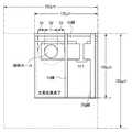
次に、図2を用いて1画素の構成を説明する。放射線検出パネル1の1画素内には、変換素子2である光電変換素子と、スイッチ素子3であるTFTが配置されている。また、画素内には、Sig線と、Vg線と、Vs線とが配置されている。図2では画素ピッチが150μmの例が示されている。Cc、Ctについては後述する。 Next, the configuration of one pixel will be described with reference to FIG. In one pixel of the
次に、図3を用いて放射線検出パネル1の層構成を説明する。図3は図2のA−A’線における断面図である。図3において10は絶縁基板である。信号転送用スイッチ素子3であるTFTは、絶縁基板10上に形成された第1の導電層11、第1の絶縁層12、第1の半導体層13、第1の不純物半導体層14、第2の導電層15から構成されている。第1の不純物半導体層14は、n型の半導体層である。 Next, the layer configuration of the
第1の導電層11はスイッチ素子3のゲート電極及びゲート線(Vg線)として、第1の絶縁層12はスイッチ素子3のゲート絶縁膜として用いられている。第1の半導体層13はスイッチ素子3のチャネルとして、第1の不純物半導体層14はオーミックコンタクト層として用いられる。第2の導電層15はスイッチ素子3のソース若しくはドレイン電極、信号線(Sig線)として用いられている。信号線(Sig線)は、ゲート線(Vg線)と交差している。換言すると、信号線(Sig線)は、ゲート線(Vg線)と部分的に重なり合っている。 The first
第2の導電層15の上層には層間絶縁層16が配置され、層間絶縁層16上に変換素子2を構成するMIS型の光電変換素子が積層されている。すなわち、スイッチ素子3と変換素子2との間に層間絶縁層16が配置されている。変換素子2は、第3の導電層17、第2の絶縁層18、第2の半導体層(光電変換層)19から構成されている。更に、第2の不純物半導体層20、第4の導電層21、第5の導電層22から構成されている。第2の不純物半導体層20は、n型の半導体層である。 An interlayer insulating
第3の導電層17は変換素子2の下電極として用いられ、第2の絶縁層18は変換素子2の絶縁層として用いられている。第2の半導体層19は変換素子2の光電変換層として、第2の不純物半導体層20は変換素子2のホールブロッキング層として用いられている。第4の導電層21は変換素子2の上電極またはバイアス線(Vs線)として用いられ、第5の導電層22はバイアス線(Vs線)から供給されるバイアス電圧を変換素子2の全体に印加するための電極として用いられている。 The third
第5の導電層22の上層には、第3の絶縁層23、保護層24、接着層25、X線を可視光に波長変換するためのシンチレータ層(蛍光体層)26が順次形成されている。接続ホール27は変換素子2とスイッチ素子3を接続する。接続ホール27については後述する。 On the fifth
ここで、従来の放射線検出装置において画像ムラが生じる原因について説明する。図2に示すように1画素におけるSig線(第2の導電層15)とそれに交差する第1の導電層11との重なり容量の総和をCaとする。 Here, the cause of image unevenness in the conventional radiation detection apparatus will be described. As shown in FIG. 2, let Ca be the sum of the overlapping capacitances of the Sig line (second conductive layer 15) and the first
容量Caは図2及び図3に示すように第1の絶縁層12を間に有するSig線(第2の導電層15)とVg線(第1の導電層11)から形成される重なり容量Ccを含んでいる。また、容量Caは第1の絶縁層12と第1の半導体層13から形成されるスイッチ素子(TFT)3のソース若しくはドレイン電極(第2の導電層15)とゲート電極(第1の導電層11)の重なり容量Ctを含んでいる。即ち、容量Ca=Cc+Ctである。図2にCc、Ctの領域が斜線で示されている。 As shown in FIGS. 2 and 3, the capacitor Ca is an overlapping capacitor Cc formed from a Sig line (second conductive layer 15) and a Vg line (first conductive layer 11) having the first insulating
例えば、Ccの面積を100μm2、Ctの面積を25μm2、第1の絶縁層12の比誘電率を6、第1の絶縁層12の膜厚を300nm、第1の半導体層13の比誘電率を12、第1の半導体層13の膜厚を200nmとする。For example, the area of Cc is 100 μm2 , the area of Ct is 25 μm2 , the relative dielectric constant of the first insulating
一方、1画素におけるSig線と変換素子2との重なり面積をS、層間絶縁層16の膜厚をd、層間絶縁層16の比誘電率をε、真空誘電率をε0とする。この場合、Sig線と変換素子2の下電極層(第3の導電層)との重なり容量Csは、
Cs=ε0×ε×S/dとなる。On the other hand, the overlapping area of the Sig line and the
Cs = ε0 × ε × S / d.
例えば、S=950μm2、ε=3とすると、膜厚dと容量Ca及び膜厚dと容量Csの関係は図4に示す通りとなる。For example, when S = 950 μm2 and ε = 3, the relationship between the film thickness d and the capacitance Ca and the relationship between the film thickness d and the capacitance Cs is as shown in FIG.
図4に示すように、従来の放射線撮像装置と同様に、例えば、層間絶縁層16の膜厚dを500nmとした場合、Caに比べCsが非常に大きい。また、層間絶縁層16の膜厚によりCsが大きく変化することが分かる。よって、基板の面内において層間絶縁層16の膜厚がばらつくことにより、Sig線に寄生する容量の総和Ca+Csがばらつく。その結果、基板内でノイズ量がばらつき、画像ムラが生じる。 As shown in FIG. 4, when the film thickness d of the interlayer insulating
このことから、層間絶縁層16の膜厚はCsがCaと同等若しくはそれ以下となるように設定することが好ましい。よって、本実施形態では、層間絶縁層16の膜厚が、
Ca≧ε0×ε×S/d
の関係を満たす膜厚に、一例では1.5μm以上に設定されており、この点が従来例と大きく異なる。即ち、基板内において層間絶縁層16の膜厚がばらついた場合でも各Sig線の寄生容量はほぼ同等となり、画像ムラを低減することが可能となる。Therefore, it is preferable to set the film thickness of the interlayer insulating
Ca ≧ ε0 × ε × S / d
In an example, the film thickness satisfying the above relationship is set to 1.5 μm or more, which is greatly different from the conventional example. That is, even when the film thickness of the interlayer insulating
実際には、Caを構成する各層の膜厚も基板内で10%程度はばらつきうる。即ち、Caも基板内で10%程度ばらつきうる。このため、絶縁基板10の上においてCsがCaの最小値以下になるように層間絶縁層16の膜厚の最小値を設定することが望ましい。 Actually, the film thickness of each layer constituting Ca can vary by about 10% within the substrate. That is, Ca can also vary by about 10% within the substrate. For this reason, it is desirable to set the minimum value of the film thickness of the interlayer insulating
一方、加工性についても考慮が必要である。図5は接続ホール27およびその付近の断面図である。図5では図3と同一部分には同一符号を付している。図5を用いて変換素子2とスイッチ素子3とを接続するための接続ホール27の加工性について説明する。 On the other hand, it is necessary to consider workability. FIG. 5 is a cross-sectional view of the
図5に示すように接続ホール27内には、変換素子2を構成する各層が配置されている。接続ホール27のテーパー角度が急峻な場合、第2の絶縁層18による変換素子2の下電極(第3の導電層17)のカバレッジが不安定となり、変換素子2の下電極(第3の導電層17)と光電変換層(第2の半導体層19)とが導通する可能性がある。 As shown in FIG. 5, the layers constituting the
このため、接続ホール27の形状は、例えば、層間絶縁層16のテーパー角度が45°以下の緩やかな形状にするとよい。特に、感光性を有する材料で層間絶縁層16を形成する場合、接続ホールのボトムからフラットな面までの横方向(基板の面に沿った方向)の距離(図5中のLf)は、膜厚の約2倍程度、即ち、2d程度以上であることが好ましい。 For this reason, the shape of the
また、接続ホール27の寸法精度を向上させるためには、十分な露光量と十分な現像時間を確保し、基板の面内または基板間における層間絶縁層16の膜厚や材料の感度といった種々のばらつきの影響を小さくしなければならない。このため、寸法精度の観点から接続ホール27のボトム径(図5中のLb)は層間絶縁層16の膜厚の約3倍以上、即ち、3d以上であることが好ましい。 In addition, in order to improve the dimensional accuracy of the
よって、接続ホール27の直径は7d程度であることが好ましい。更に、センサ特有の構造として、Vs線を最上部に配置する必要があり、また、画素領域外での配線の取り出し等を考慮すると、望ましくはVs線を画素中央部に配置する構成がよい。 Therefore, the diameter of the
図6に示すように、例えば、画素ピッチが100μmの場合、スイッチ素子(TFT)や配線が1画素に占める割合が大きくなる。その結果、接続ホールは少なくとも画素ピッチの1/2に配置できるサイズにすることが好ましい。これは、画素ピッチが小さくなればなるほど重要なポイントとなる。 As shown in FIG. 6, for example, when the pixel pitch is 100 μm, the ratio of the switch element (TFT) and the wiring to one pixel increases. As a result, it is preferable that the connection hole has a size that can be arranged at least 1/2 of the pixel pitch. This becomes an important point as the pixel pitch becomes smaller.
図6において、例えば、層間絶縁層の膜厚を6.0μmとした場合、接続ホールのトップの直径(図6中の破線)は、7×6.0μm=42.0μmとなる。即ち、実質、接続ホールを配置可能な領域は画素ピッチの半分程度となる。よって、画素ピッチをPとした場合、層間絶縁層の膜厚が、
2Lf+Lb=7d≦P/2
を満たすことにより、層間絶縁層の加工安定性の確保が可能となる。In FIG. 6, for example, when the thickness of the interlayer insulating layer is 6.0 μm, the top diameter of the connection hole (broken line in FIG. 6) is 7 × 6.0 μm = 42.0 μm. That is, the area where the connection holes can be arranged is substantially half the pixel pitch. Therefore, when the pixel pitch is P, the film thickness of the interlayer insulating layer is
2Lf + Lb = 7d ≦ P / 2
By satisfying the above, it is possible to ensure the processing stability of the interlayer insulating layer.
実際には、接続ホール内にVs線を配置した場合、Vs線を形成する際に接続ホール内とそうでない部分(層間絶縁層がフラットな部分)とではレジスト膜厚(Vs線をパタニングするためのエッチングマスクを形成するために塗布されるレジスト膜の厚さのこと。)が異なり、結果、Vs線の線幅が異なることになる。このため、Vs線は接続ホールの外側のフラットな面に配置するべきであり、更にパターンズレ等を考慮すると、Vs線と接続ホールの間には一定の間隔を設ける必要がある。よって、上述のように層間絶縁層の膜厚が6.0μm程度であれば、Vs線と接続ホールの間に間隔を設けることも可能である。図6では、バイアス線(Vs線)は、放射線入射側からみてスイッチ素子(TFT)と接続ホールとの間に配置されている。 Actually, when the Vs line is disposed in the connection hole, the resist film thickness (for patterning the Vs line) is different between the connection hole and the portion where the Vs line is formed (the portion where the interlayer insulating layer is flat). The thickness of the resist film applied to form the etching mask is different, and as a result, the line width of the Vs line is different. For this reason, the Vs line should be arranged on a flat surface outside the connection hole. Further, in consideration of pattern shift or the like, it is necessary to provide a certain distance between the Vs line and the connection hole. Therefore, as described above, if the thickness of the interlayer insulating layer is about 6.0 μm, it is possible to provide a gap between the Vs line and the connection hole. In FIG. 6, the bias line (Vs line) is disposed between the switch element (TFT) and the connection hole as viewed from the radiation incident side.
以上のことから、本実施形態においては、層間絶縁層の膜厚を1.5μmから6.0μm程度に設定することにより、積層型の放射線検出装置において、層間絶縁層の加工安定性を確保することが可能となる。更に、層間絶縁層の膜厚ばらつきによる画像ムラを低減することが可能となる。 From the above, in this embodiment, by setting the film thickness of the interlayer insulating layer from about 1.5 μm to about 6.0 μm, the processing stability of the interlayer insulating layer is ensured in the stacked radiation detection apparatus. It becomes possible. Further, it is possible to reduce image unevenness due to variations in the film thickness of the interlayer insulating layer.
なお、図1には3×3画素がマトリクス状に配置されているが、実際には、例えば、2000×2000の画素がマトリクス状に配置されている。また、光電変換素子とシンチレータ層を組み合わせた間接型の放射線検出装置を示したが、本発明はこれに限ることはない。即ち、光電変換素子に代えて、X線、γ線、或いはα線、β線等の粒子線を直接電荷に変換するアモルファスセレン等の半導体層を電極間に挟んだ変換素子を用いた直接型の放射線検出装置においても同様の効果が得られる。 In FIG. 1, 3 × 3 pixels are arranged in a matrix, but actually, for example, 2000 × 2000 pixels are arranged in a matrix. Moreover, although the indirect type radiation detection apparatus which combined the photoelectric conversion element and the scintillator layer was shown, this invention is not limited to this. That is, instead of a photoelectric conversion element, a direct type using a conversion element in which a semiconductor layer of amorphous selenium or the like that directly converts X-rays, γ-rays, or α-rays, β-rays, etc. into a charge is sandwiched between electrodes. The same effect can be obtained with this radiation detection apparatus.
また、間接型の放射線検出パネルの変換素子は、MIS型光電変換素子とは別の光電変換素子、例えば、PIN型の光電変換素子を用いても構わない。更に、保護層上に接着層を介してシンチレータ層を積層させた例を示したが、保護層上に直接CsI等のシンチレータ層を設けた放射線検出装置でもよい。 Further, as the conversion element of the indirect radiation detection panel, a photoelectric conversion element different from the MIS type photoelectric conversion element, for example, a PIN type photoelectric conversion element may be used. Furthermore, although the example which laminated | stacked the scintillator layer on the protective layer through the contact bonding layer was shown, the radiation detection apparatus which provided the scintillator layer, such as CsI, directly on the protective layer may be sufficient.
上記のように、本実施形態では、入射放射線がX線、γ線、或いはα線、β線等の粒子線の場合を説明したが、入射放射線が可視光、赤外線の場合はシンチレータ層を含まずに光電変換素子で変換する検出装置となる。 As described above, in the present embodiment, the case where the incident radiation is X-ray, γ-ray, or particle beam such as α-ray, β-ray, etc. has been described, but when the incident radiation is visible light or infrared, a scintillator layer is included. It becomes a detection apparatus which converts with a photoelectric conversion element.
(第2の実施形態)
次に、本発明の第2の実施形態について説明する。図7は本実施形態の構成図、図8は1画素の平面図、図9は図8のB−B’線における断面図である。図10は層間絶縁層の膜厚と信号線に付加される容量の関係を示す。図7〜図9では図1〜図3と同一部分には同一符号を付している。(Second Embodiment)
Next, a second embodiment of the present invention will be described. 7 is a configuration diagram of the present embodiment, FIG. 8 is a plan view of one pixel, and FIG. 9 is a cross-sectional view taken along line BB ′ of FIG. FIG. 10 shows the relationship between the film thickness of the interlayer insulating layer and the capacitance added to the signal line. 7 to 9, the same parts as those in FIGS. 1 to 3 are denoted by the same reference numerals.
本実施形態では、1画素は変換素子(光電変換素子)2、信号転送用スイッチ素子である信号転送用TFT3、リセット用スイッチ素子であるリセット用TFT6を含む。また、1画素はバイアス線(Vs線)、ゲート線(Vg線)、信号線(Sig線)の他に、ゲート線(Vr線)、リセット線(Vt線)を含む。 In the present embodiment, one pixel includes a conversion element (photoelectric conversion element) 2, a
放射線検出パネル1内には、上記のような複数の画素がマトリクス状に配置されている。変換素子2には、例えば、MIS型の光電変換素子が用いられる。信号転送用TFT3のゲートはゲート駆動装置4によって駆動される第1のゲート線(Vg線)に接続され、ゲート駆動装置4からの信号によって駆動される。リセット用スイッチ素子であるリセット用TFT6のゲートはゲート駆動装置4によって駆動される第2のゲート線(Vr線)に接続され、ゲート駆動装置4からの信号によって駆動される。リセット用TFT6は光電変換素子2の残留電荷を除去するのに用いられる。 In the
信号転送用TFT3の一方の端子(ドレイン又はソース)は信号線(Sig線)に接続され、変換素子2からの信号は信号転送用TFT3によって信号線(Sig線)に転送され、信号線(Sig線)を通して読み出し装置5によって読み出される。また、リセット用TFT6の一方の端子(ドレイン又はソース)はリセット線(Vt線)に接続されていて、リセット線(Vt線)からリセット用TFT6を介してバイアス電圧を光電変換素子2に印加することで残留電荷が除去される。 One terminal (drain or source) of the
次に、図7を用いて動作原理について説明する。まず、変換素子2であるMIS型の光電変換素子の第2の半導体層が空乏化するようにバイアス線(Vs線)から光電変換素子2にバイアスが印加される。この状態で、被検体(図示せず)に向けて曝射されたX線は被検体により減衰を受けて透過し、図示しないシンチレータ層で可視光に変換され、この可視光が変換素子2に入射し、電荷に変換される。 Next, the principle of operation will be described with reference to FIG. First, a bias is applied from the bias line (Vs line) to the
この電荷は、ゲート駆動装置4からゲート線(Vg線)に印加されるゲート駆動パルスにより信号転送用スイッチ素子である信号転送用TFTを導通状態にすることにより信号線(Sig線)に転送され、読み出し装置5により外部に読み出される。その後、ゲート駆動装置4からゲート線(Vr線)にゲート駆動パルスが印加され、リセット用スイッチ素子であるリセット用TFT6を導通状態にする。 This electric charge is transferred to the signal line (Sig line) by turning on the signal transfer TFT, which is a signal transfer switch element, by the gate drive pulse applied from the
この間にリセット線(Vt線)に光電変換素子2をリセットするためのバイアスが印加され、光電変換素子2で発生し転送しきれなかった残留電荷が除去される。以上の動作を繰り返すことにより、1画像の画像信号が得られ、更に繰り返し1画像の画像信号を取得することにより動画像が得られる。 During this time, a bias for resetting the
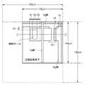
次に、図8を用いて本実施形態の1画素の構成を説明する。図8に示すように1画素内には、変換素子2である光電変換素子と、信号転送用スイッチ素子である信号転送用TFT3と、リセット用スイッチ素子であるリセット用TFT6が配置されている。また、信号線(Sig線)、ゲート線(Vg線)、ゲート線(Vr線)、リセット線(Vt線)、及びバイアス線(Vs線)が配置されている。図8は図2と同様に画素ピッチが150μmの例を示す。 Next, the configuration of one pixel of this embodiment will be described with reference to FIG. As shown in FIG. 8, in one pixel, a photoelectric conversion element that is the
次に、図9を用いて放射線検出パネルの層構成を説明する。図9は図8のB−B’線における断面図である。図9において10は絶縁基板である。信号転送用TFT3とリセット用TFT6は、絶縁基板10上に形成された第1の導電層11、第1の絶縁層12、第1の半導体層13、第1の不純物半導体層(オーミックコンタクト層)14、第2の導電層15から構成されている。 Next, the layer configuration of the radiation detection panel will be described with reference to FIG. FIG. 9 is a cross-sectional view taken along line B-B ′ of FIG. 8. In FIG. 9,
第1の導電層11は信号転送用TFT3のゲート電極、ゲート線(Vg線)、リセット用TFT6のゲート電極、ゲート線(Vr線)として用いられ、第1の絶縁層12はゲート絶縁膜として用いられている。第1の半導体層13は信号転送用TFT3及びリセット用TFT6のチャネルとして用いられている。第1の不純物半導体層14はオーミックコンタクト層として用いられている。 The first
第2の導電層15は信号転送用TFT3及びリセット用TFT6のソース若しくはドレイン電極、信号線(Sig線)、リセット線(Vt線)として用いられている。第2の導電層15の上層には層間絶縁層16が形成され、その層間絶縁層16上に変換素子2を構成するMIS型光電変換素子が積層されている。 The second
変換素子2は、第3の導電層17、第2の絶縁層18、第2の半導体層(光電変換層)19、第2の不純物半導体層(ホールブロッキング層)20、第4の導電層21、第5の導電層22から構成されている。 The
第3の導電層17は光電変換素子2の下電極として用いられ、第2の絶縁層18は光電変換素子の絶縁層として用いられている。第2の半導体層19は光電変換素子の光電変換層として用いられ、第2の不純物半導体層20は光電変換素子のホールブロッキング層として用いられている。 The third
第4の導電層21は光電変換素子の上電極またはVs線として用いられ、第5の導電層22はVs線から供給されるバイアス電圧を変換素子全体に印加するための電極として用いられている。更に、その上層に第3の絶縁層23、保護層24、接着層25、X線を可視光に波長変換するシンチレータ層(蛍光体層)26が順次形成されている。 The fourth
次に、信号線(Sig線)の寄生容量について説明する。1画素におけるSig線と第1の導電層11との重なり容量の総和をCaとする。この場合、容量Caは図8及び図9に示すように第1の絶縁層12を間に有するSig線(第2の導電層)とVg線(第1の導電層)から形成される重なり容量Ccを含んでいる。 Next, the parasitic capacitance of the signal line (Sig line) will be described. Let Ca be the sum of the overlapping capacities of the Sig line and the first
また、容量Caは第1の絶縁層12を間に有するSig線(第2の導電層)とVr線(第1の導電層)から形成される重なり容量Ccを含んでいる。更に、容量Caは第1の絶縁層12と第1の半導体層13から形成されるTFT(信号転送用TFT)のソース若しくはドレイン電極(第2の導電層)と、ゲート電極(第1の導電層)との重なり容量Ctを含んでいる。即ち、Ca=2×Cc+Ctである。図8中にCc、Ctの領域が斜線で示されている。 The capacitor Ca includes an overlapping capacitor Cc formed by a Sig line (second conductive layer) and a Vr line (first conductive layer) having the first insulating
一方、Sig線と光電変換素子の下電極層(第3の導電層)との重なり容量Csは、第1の実施形態と同様に、Cs=ε0×ε×S/dとなる。
εは層間絶縁層16の比誘電率、ε0は真空誘電率である。On the other hand, the overlapping capacitance Cs between the Sig line and the lower electrode layer (third conductive layer) of the photoelectric conversion element is Cs = ε0 × ε × S / d, as in the first embodiment.
epsilon is the dielectric constant of the interlayer insulating
ここで、層間絶縁層16に第1の絶縁層12と同様の膜を使用した場合、ε=6となる。その他、各部の面積及び各層の膜厚及び各層の比誘電率は第1の実施形態と同じとすると、膜厚dと容量Ca及び膜厚dと容量Csの関係は図10に示す通りとなる。 Here, when a film similar to the first insulating
図10に示すように、従来の放射線撮像装置と同様に、例えば、層間絶縁層16の膜厚dを500nmとした場合、Caに比べCsが非常に大きく、層間絶縁層の膜厚によりCsが大きく変化することが分かる。よって、基板の面内において層間絶縁層の膜厚がばらつくことにより、Sigに寄生する容量の総和Ca+Csがばらつく。その結果、従来の放射線撮像装置においては基板内でノイズ量がばらつき、画像ムラが生じる。 As shown in FIG. 10, when the film thickness d of the interlayer insulating
このことから、第1の実施形態と同様に層間絶縁層16の膜厚は、CsがCaと同等若しくはそれ以下となるように設定することが好ましい。よって、本実施形態においては、層間絶縁層の膜厚が、
Ca≧ε0×ε×S/d
の関係を満たす膜厚に、一例では2.5μm以上に設定されており、この点が従来例と大きく異なる。即ち、基板内において層間絶縁層の膜厚がばらついた場合でも、各Sig線の寄生容量はほぼ同等となり、画像ムラを低減することが可能となる。Therefore, as in the first embodiment, the film thickness of the interlayer insulating
Ca ≧ ε0 × ε × S / d
In an example, the film thickness satisfying the above relationship is set to 2.5 μm or more, which is greatly different from the conventional example. That is, even when the film thickness of the interlayer insulating layer varies in the substrate, the parasitic capacitances of the Sig lines are almost equal, and image unevenness can be reduced.
一方、第1の実施形態と同様に層間絶縁層16の膜厚が、
2Lf+Lb=7d≦P/2
を満たすことにより、層間絶縁層の加工安定性の確保が可能となる。On the other hand, as in the first embodiment, the thickness of the interlayer insulating
2Lf + Lb = 7d ≦ P / 2
By satisfying the above, it is possible to ensure the processing stability of the interlayer insulating layer.
以上のことから、画素ピッチを100μm程度まで考慮した場合、層間絶縁層の膜厚を2.5μmから6.0μm程度に設定することにより、積層型の放射線検出装置において層間絶縁層の加工安定性を確保することが可能となる。また、層間絶縁層の膜厚ばらつきによる画像ムラを低減させることが可能となる。当然、画素ピッチが100μmより小さくなる場合には、層間絶縁層の膜厚は6.0μmより薄くする必要がある。 From the above, when the pixel pitch is taken into consideration up to about 100 μm, the processing stability of the interlayer insulating layer in the stacked type radiation detector is set by setting the film thickness of the interlayer insulating layer from about 2.5 μm to about 6.0 μm. Can be secured. In addition, it is possible to reduce image unevenness due to variations in the thickness of the interlayer insulating layer. Of course, when the pixel pitch is smaller than 100 μm, the film thickness of the interlayer insulating layer needs to be smaller than 6.0 μm.
なお、図7には3×3画素を示しているが、実際には、例えば、2000×2000画素が配置されている。また、本実施形態では光電変換素子とシンチレータを組み合わせた間接型の放射線検出装置を示したが、本発明はこれに限ることはない。即ち、光電変換素子に代えて、X線、γ線、或いはα線、β線等の粒子線を直接電荷に変換するアモルファスセレン等の半導体層を電極間に挟んだ変換素子を用いた直接型の放射線検出装置においても同様の効果が得られる。 Although FIG. 7
また、間接型の放射線検出パネルの変換素子は、MIS型光電変換素子とは別の光電変換素子、例えば、PIN型の光電変換素子を用いても構わない。更に、本実施形態では保護層上に接着層を介してシンチレータ層を積層させた例を示したが、保護層上に直接CsI等のシンチレータ層を設けた放射線検出装置でもよい。上記の各実施形態では、入射放射線がX線、γ線、或いはα線、β線等の粒子線の場合を説明したが、入射放射線が可視光、赤外線の場合はシンチレータ層は含まずに光電変換素子で変換する放射線検出装置となる。 Further, as the conversion element of the indirect radiation detection panel, a photoelectric conversion element different from the MIS type photoelectric conversion element, for example, a PIN type photoelectric conversion element may be used. Furthermore, in the present embodiment, an example in which a scintillator layer is laminated on the protective layer via an adhesive layer is shown, but a radiation detection apparatus in which a scintillator layer such as CsI is directly provided on the protective layer may be used. In each of the above embodiments, the case where the incident radiation is X-ray, γ-ray, or particle beam such as α-ray, β-ray, etc. has been described. However, when the incident radiation is visible light or infrared light, the scintillator layer is not included. It becomes a radiation detection apparatus which converts with a conversion element.
(第3の実施形態)
次に、本発明の第3の実施形態について説明する。図11は1画素の平面図、図12は図11のC−C’線における断面図である。図11、図12では図1〜図3と同一部分には同一符号を付している。
まず、図11を用いて1画素の構成を説明する。放射線検出パネルの1画素内には、実施形態1と同様に変換素子2である光電変換素子と、スイッチ素子3であるTFTが配置されている。また、1画素内には、Sig線と、Vg線と、Vs線とが配置されている。本実施形態においては、光電変換素子とTFTを接続する接続ホールが長方形、若しくは楕円形である点が、実施形態1と異なる点である。(Third embodiment)
Next, a third embodiment of the present invention will be described. 11 is a plan view of one pixel, and FIG. 12 is a cross-sectional view taken along the line CC ′ of FIG. 11 and 12, the same parts as those in FIGS. 1 to 3 are denoted by the same reference numerals.
First, the configuration of one pixel will be described with reference to FIG. In one pixel of the radiation detection panel, a photoelectric conversion element that is the
次に、図12を用いて本実施形態の1画素の構成を説明する。図12は図11のC−C’線における断面図である。図12において10は絶縁基板である。信号転送用スイッチ素子3であるTFTは、絶縁基板10の上に形成されており、TFTのソース若しくはドレイン電極、Sig線を形成する第2の導電層15の上層には第1の層間絶縁層16と第2の層間絶縁層28が配置されている。この2種類の層間絶縁層が配置されている点が、実施形態1と異なる点である。具体的には、第1の層間絶縁層16に第1の絶縁層12と同様のε=6の膜を、また第2の層間絶縁層28にε=3の膜を使用している。更に、第2の層間絶縁層28上には、変換素子2を構成するMISの型光電変換素子が積層されている。 Next, the configuration of one pixel of this embodiment will be described with reference to FIG. 12 is a cross-sectional view taken along line C-C ′ of FIG. 11. In FIG. 12, 10 is an insulating substrate. The TFT that is the signal
ここで、信号線(Sig線)の寄生容量について説明する。図11に示すように1画素におけるSig線(第2の導電層)と第1の導電層11との重なり容量の総和をCaとする。この場合、容量Caは図11及び図12に示すように第1の絶縁層12を間に有するSig線(第2の導電層)とVg線(第1の導電層)から形成される重なり容量Ccを含んでいる。また、容量Caは第1の絶縁層12と第1の半導体層13から形成されるTFTのソース若しくはドレイン電極(第2の導電層)とゲート電極(第1の導電層)の重なり容量Ctとの総和となる。即ち、容量Ca=Cc+Ctである。図11にCc、Ctの領域が斜線で示されている。 Here, the parasitic capacitance of the signal line (Sig line) will be described. As shown in FIG. 11, the total sum of the overlapping capacities of the Sig line (second conductive layer) and the first
一方、1画素におけるSig線と変換素子2の重なった部分において、第1の層間絶縁層16の容量をC16、第2の層間絶縁層28の容量をC28とする。この場合、Sig線と変換素子2の下電極層(第3の導電層)との重なり容量Csは、
Cs=(C16×C28)/(C16+C28)となる。
上述したように、基板の面内において第1の層間絶縁層16、または第2の層間絶縁層28の膜厚がばらつくことにより、Sig容量の総和Ca+Csがばらつく。その結果、基板内でノイズ量がばらつき、画像ムラが生じる場合がある。On the other hand, in the portion where the Sig line and the
Cs = (C16 × C28 ) / (C16 + C28 ).
As described above, when the film thickness of the first
このことから、第1の層間絶縁層16、及び第2の層間絶縁層28の膜厚は、実施形態1、及び実施形態2と同様に、CsがCaと同等若しくはそれ以下となるように設定することが好ましい。よって、本実施形態では、第1の層間絶縁層16、及び第2の層間絶縁層28の膜厚が、
Ca≧(C16×C28)/(C16+C28)
の関係を満たす膜厚に設定される。即ち、基板の面内において第1の層間絶縁層16、または第2の層間絶縁層28の膜厚がばらついた場合でも各Sig線の寄生容量はほぼ同等となり、画像ムラを低減することが可能となる。Therefore, the film thicknesses of the first
Ca ≧ (C16 × C28 ) / (C16 + C28 )
Is set to a film thickness satisfying the above relationship. That is, even when the film thickness of the first
なお、層間絶縁層が3層以上配置される場合には、上記考え方と同様に、Ca≧Csの関係を満たすよう各層間絶縁層の膜厚を設定することが望ましい。 When three or more interlayer insulating layers are arranged, it is desirable to set the film thickness of each interlayer insulating layer so as to satisfy the relationship of Ca ≧ Cs, similarly to the above-described concept.
また、接続ホールの加工形状については、実施形態1において説明したように、テーパー角度が45°以下の緩やかな形状にするとよい。本実施形態においては、第2の層間絶縁層28が感光性を有するため、接続ホールのボトムからフラットな面までの距離(図5中のLf)は、層間絶縁層の膜厚をd28とした場合、2d28程度となる。Further, as described in the first embodiment, the processing shape of the connection hole may be a gentle shape having a taper angle of 45 ° or less. In the present embodiment, since the second
一方、Sig線、及びVg線は第1の層間絶縁層16、及び第2の層間絶縁層28を介して変換素子2と容量を形成する。このため、層間絶縁層の下層に配置される各配線の容量を一定に保つために、各配線上の層間絶縁層の膜厚は一定であることが望ましい。即ち、Sig線と接続ホールの間隔、及びVg線と接続ホールの間隔は2d28以上であることが望ましい。On the other hand, the Sig line and the Vg line form a capacitance with the
また、実施形態1で説明したように、接続ホールより上層に配置される配線、特にVs線は加工精度の安定性の観点から、接続ホールの外側のフラットな面に配置する必要がある。即ち、Vs線と接続ホールとの間隔は2d28以上であることが望ましい。画素ピッチが小さい場合には、図11のように接続ホールとSig線の間にVs線を配置することにより、Sig線とVs線の間隔を十分確保することが可能となる。Further, as described in the first embodiment, the wiring arranged above the connection hole, particularly the Vs line, needs to be arranged on a flat surface outside the connection hole from the viewpoint of stability of processing accuracy. That is, the distance between the Vs line and the connection hole is desirably 2d28 or more. When the pixel pitch is small, it is possible to secure a sufficient interval between the Sig line and the Vs line by arranging the Vs line between the connection hole and the Sig line as shown in FIG.
また、本実施形態のように接続ホールの形状が長方形、又は楕円形の場合には、寸法精度向上の観点から接続ホールのボトム径(図5中のLb)は、図11のように接続ホールの短辺にて3d28以上を確保すればよい。即ち、実施形態1、及び実施形態2と同様に第2の層間絶縁層28の膜厚が、2Lf+Lb=d28≦P/2を満たすことにより、第2の層間絶縁層の加工精度の安定性の確保が可能となる。Further, when the shape of the connection hole is rectangular or elliptical as in the present embodiment, the bottom diameter of the connection hole (Lb in FIG. 5) is set as shown in FIG. It is sufficient to secure 3d28 or more on the short side. That is, the stability of the processing accuracy of the second interlayer insulating layer is achieved when the film thickness of the second
(第4の実施形態)
図13は本発明の放射線検出装置を用いた放射線撮像システムの一実施形態を示す構成図である。本実施形態において放射線とはX線、α線、β線、γ線をいうが、特にX線の場合を説明する。図13に示すように放射線源であるX線チューブ6050で発生したX線6060は患者あるいは被験者6061の胸部6062を透過し、シンチレータを有する放射線検出装置6040に入射する。(Fourth embodiment)
FIG. 13 is a block diagram showing an embodiment of a radiation imaging system using the radiation detection apparatus of the present invention. In the present embodiment, radiation means X-rays, α-rays, β-rays, and γ-rays. The case of X-rays in particular will be described. As shown in FIG. 13,
この入射したX線には患者6061の体内部の情報が含まれている。X線の入射に対応してシンチレータは発光し、これを光電変換して電気的情報を得る。この情報はディジタルに変換され、放射線検出装置6040からの信号を処理する信号処理手段となるイメージプロセッサ6070により画像処理され、制御室の表示手段となるディスプレイ6080で観察できる。 This incident X-ray includes information inside the body of the
この情報は電話回線6090等の伝送処理手段により遠隔地へ転送でき、別の場所のドクタールーム等に設置された表示手段となるディスプレイ6081に表示又は光ディスク等の記録手段に保存することができ、遠隔地の医師が診断することも可能である。また、記録手段となるフィルムプロセッサ6100により記録媒体となるフィルム6110に記録することもできる。 This information can be transferred to a remote location by transmission processing means such as a
なお、本発明に係る放射線撮像システムは、放射線検出装置6040と、以下の手段のうち1つ又2以上の手段を具備することで構成しても良い。即ち、信号処理手段(イメージプロセッサ6070)、記録手段(フィルムプロセッサ6100等)、表示手段(ディスプレイ6080)、伝送処理手段(電話回線6090等)、放射線源(X線チューブ6050)のうち1つ又は2以上を具備しても良い。 The radiation imaging system according to the present invention may be configured by including the
Claims (6)
Translated fromJapanese前記スイッチ素子のゲートに接続されたゲート線と、
前記ゲート線と交差して配置され、前記スイッチ素子のソース又はドレインに電気的に接続された信号線と、前記変換素子と前記スイッチ素子との間、及び、前記変換素子と前記信号線との間に配置された層間絶縁層と、
を有する放射線検出装置であって、
1画素における前記信号線と前記ゲート線との重なり容量をCc、1画素における前記スイッチ素子のゲートと前記スイッチ素子のソース又はドレインとの間の容量をCt、1画素における前記信号線と前記変換素子との重なり面積をS、前記層間絶縁層の膜厚をd、前記層間絶縁層の比誘電率をε、前記層間絶縁層の真空誘電率をε0とした場合に、
Cc+Ct≧ε0×ε×S/d
を満たすように、Cc、Ct、ε、S、dが決定されていることを特徴とする放射線検出装置。A conversion element for converting incident radiation into charge, a plurality of pixels anda switch element for transferring charges of the conversion elements,
A gate lineconnected to the gate of the switch element;
A signal linedisposed across the gate line andelectrically connected to the source or drain of theswitch element, between the conversion element and the switch element, and between the conversion element and the signal line An interlayer insulating layer disposed between,
A radiation detection apparatus comprising:
Theoverlap capacitance between the gate line and the signal line inone pixelCc, 1 is the source of the gate and the switching element of the switching element also in the pixel and the signal line inCt, one pixelcapacitance between the drain conversion the overlapping area of the element S, the thickness of the interlayer insulating layer d, the dielectric constant of the interlayer insulating layer epsilon, the vacuum dielectric constant of the interlayer insulating layerwhen the .epsilon.0,
Cc + Ct ≧ ε0 × ε × S / d
A radiation detection apparatus, wherein Cc, Ct, ε, S, and d are determined so asto satisfy
前記変換素子と前記スイッチ素子とを電気的に接続するための前記層間絶縁層の接続ホールのテーパー角度は45°以下であることを特徴とする請求項1に記載の放射線検出装置。When the pixel pitch of the plurality of pixels is P, 7d ≦ P / 2 is satisfied,
The radiation detection apparatus according to claim 1, wherein a taper angle of a connection hole of the interlayer insulating layer for electrically connecting the conversion element and the switch element is 45 ° or less.
前記バイアス線は、放射線入射側から見て、前記変換素子と前記スイッチ素子とを電気的に接続するための前記層間絶縁層の接続ホールと前記スイッチ素子との間に配置されたことを特徴とする請求項1に記載の放射線検出装置。A bias line for applying a bias voltage to the conversion element;
The bias line is disposed between a connection hole of the interlayer insulating layer and the switch element for electrically connecting the conversion element and the switch element when viewed from the radiation incident side. The radiation detection apparatus according to claim 1.
前記転送用スイッチ素子のゲートに電気的に接続された第1のゲート線と、
前記リセット用スイッチ素子のゲートに電気的に接続された第2のゲート線と、
前記第1及び第2のゲート線と交差して配置され、前記転送用スイッチ素子のソース又はドレインに電気的に接続された信号線と、
前記転送用スイッチ素子と前記変換素子との間、前記リセット用スイッチ素子と前記変換素子との間、及び、前記信号線と前記変換素子との間に配置された層間絶縁層と、
を有する放射線検出装置であって、
1画素における前記信号線と前記第1のゲート線および第2のゲート線との重なり容量のそれぞれをCc、1画素における前記転送用スイッチ素子のゲートと前記転送用スイッチ素子のソース又はドレインとの間の容量をCt、1画素における前記信号線と前記変換素子との重なり面積をS、前記層間絶縁層の膜厚をd、前記層間絶縁層の比誘電率をε、前記層間絶縁層の真空誘電率をε0とした場合に、
2×Cc+Ct≧ε0×ε×S/d
を満たすように、Cc、Ct、ε、S、dが決定されていることを特徴とする放射線検出装置。A conversion element for converting incident radiation into charge, and the transfer switch for transferring charges of the conversion elements, a plurality of which anda reset switch for applying a bias voltage for resetting the conversion element Pixels,
A first gate lineelectrically connected to the gate of the transfer switch element;
A second gate lineelectrically connected to the gate of the reset switch element;
A signal line disposed across the first and second gate lines andelectrically connected to the source or drain of the transfer switch element;
An interlayer insulating layer disposed between the transfer switch element and the conversion element, between the reset switch element and the conversion element, and between the signal line and the conversion element;
A radiation detection apparatus comprising:
1respectively overlap capacitance between the signal line and the first gate line and the second gate lines in the pixelCc,first gate and the transfer switch of the transfer switch in a pixel source or the drain Ct is the capacitance between the signal line and the conversion element in one pixel, S is the thickness of the interlayer insulating layer, d is the relative dielectric constant of the interlayer insulating layer, and the interlayer insulating layer is vacuum. When the dielectric constant is ε0,
2 × Cc + Ct ≧ ε0 × ε × S / d
A radiation detection apparatus, wherein Cc, Ct, ε, S, and d are determined so asto satisfy
前記放射線検出装置からの信号を処理する信号処理手段と、
を具備することを特徴とする放射線撮像システム。The radiation detection apparatus according to claim 1 or 5,
Signal processing means for processing signals from the radiation detection device;
A radiation imaging system comprising:
Priority Applications (2)
| Application Number | Priority Date | Filing Date | Title |
|---|---|---|---|
| JP2009136710AJP5489542B2 (en) | 2008-07-01 | 2009-06-05 | Radiation detection apparatus and radiation imaging system |
| US12/493,776US8368027B2 (en) | 2008-07-01 | 2009-06-29 | Radiation detection apparatus and radiographic imaging system |
Applications Claiming Priority (3)
| Application Number | Priority Date | Filing Date | Title |
|---|---|---|---|
| JP2008172622 | 2008-07-01 | ||
| JP2008172622 | 2008-07-01 | ||
| JP2009136710AJP5489542B2 (en) | 2008-07-01 | 2009-06-05 | Radiation detection apparatus and radiation imaging system |
Publications (2)
| Publication Number | Publication Date |
|---|---|
| JP2010034520A JP2010034520A (en) | 2010-02-12 |
| JP5489542B2true JP5489542B2 (en) | 2014-05-14 |
Family
ID=41463634
Family Applications (1)
| Application Number | Title | Priority Date | Filing Date |
|---|---|---|---|
| JP2009136710AActiveJP5489542B2 (en) | 2008-07-01 | 2009-06-05 | Radiation detection apparatus and radiation imaging system |
Country Status (2)
| Country | Link |
|---|---|
| US (1) | US8368027B2 (en) |
| JP (1) | JP5489542B2 (en) |
Families Citing this family (41)
| Publication number | Priority date | Publication date | Assignee | Title |
|---|---|---|---|---|
| JP5406473B2 (en)* | 2007-07-19 | 2014-02-05 | キヤノン株式会社 | Radiation detector |
| EP3522081A1 (en) | 2009-12-04 | 2019-08-07 | Uber Technologies, Inc. | System and method for arranging transport amongst parties through use of mobile devices |
| JP2011238897A (en)* | 2010-04-13 | 2011-11-24 | Canon Inc | Detection device, manufacturing method thereof, and detection system |
| KR101736321B1 (en)* | 2010-12-22 | 2017-05-17 | 삼성디스플레이 주식회사 | Thin film transistor array substrate for X-ray detector and X-ray detector |
| JP5848047B2 (en)* | 2011-07-07 | 2016-01-27 | 富士フイルム株式会社 | Radiation detection element, radiation image capturing apparatus, and radiation image capturing system |
| FR2977977B1 (en)* | 2011-07-13 | 2013-08-30 | Trixell | METHOD FOR CONTROLLING A PHOTOSENSITIVE DETECTOR BY AUTOMATIC DETECTION OF INCIDENT RADIATION |
| JP2015005533A (en)* | 2011-10-21 | 2015-01-08 | 富士フイルム株式会社 | Radiation imaging equipment |
| JP6057511B2 (en) | 2011-12-21 | 2017-01-11 | キヤノン株式会社 | Imaging apparatus and radiation imaging system |
| JP5954983B2 (en) | 2011-12-21 | 2016-07-20 | キヤノン株式会社 | Imaging apparatus, radiation imaging system, and manufacturing method of imaging apparatus |
| TWI475676B (en)* | 2012-02-13 | 2015-03-01 | Innocom Tech Shenzhen Co Ltd | Active matrix image sensing panel and device |
| JP2013243319A (en)* | 2012-05-23 | 2013-12-05 | Konica Minolta Inc | Radiological imaging device |
| JP2014003183A (en)* | 2012-06-19 | 2014-01-09 | Canon Inc | Detection device and radiation detection system |
| JP5997512B2 (en) | 2012-06-20 | 2016-09-28 | キヤノン株式会社 | Radiation detection apparatus and imaging system |
| US8872120B2 (en)* | 2012-08-23 | 2014-10-28 | Semiconductor Energy Laboratory Co., Ltd. | Imaging device and method for driving the same |
| KR102081186B1 (en)* | 2012-11-05 | 2020-02-26 | 삼성디스플레이 주식회사 | X-ray detection device and method of driving an x-ray detection panel |
| JP6463136B2 (en) | 2014-02-14 | 2019-01-30 | キヤノン株式会社 | Radiation detection apparatus and radiation detection system |
| JP6585910B2 (en) | 2014-05-01 | 2019-10-02 | キヤノン株式会社 | Radiation imaging apparatus and radiation imaging system |
| JP6480670B2 (en) | 2014-05-01 | 2019-03-13 | キヤノン株式会社 | Radiation imaging apparatus and radiation imaging system |
| US9526468B2 (en) | 2014-09-09 | 2016-12-27 | General Electric Company | Multiple frame acquisition for exposure control in X-ray medical imagers |
| JP6555909B2 (en) | 2015-03-20 | 2019-08-07 | キヤノン株式会社 | Radiation imaging apparatus and radiation imaging system |
| JP6570315B2 (en) | 2015-05-22 | 2019-09-04 | キヤノン株式会社 | Radiation imaging apparatus and radiation imaging system |
| US9818296B2 (en) | 2015-10-16 | 2017-11-14 | Uber Technologies, Inc. | System for providing a city planning tool |
| WO2017170936A1 (en)* | 2016-04-01 | 2017-10-05 | シャープ株式会社 | Photoelectric converter and x-ray detector |
| JP6929104B2 (en) | 2017-04-05 | 2021-09-01 | キヤノン株式会社 | Radiation imaging device, radiation imaging system, control method and program of radiation imaging device |
| JP6990986B2 (en) | 2017-04-27 | 2022-01-12 | キヤノン株式会社 | Radiation imaging device, radiation imaging system, control method and program of radiation imaging device |
| JP6853729B2 (en) | 2017-05-08 | 2021-03-31 | キヤノン株式会社 | Radiation imaging device, radiation imaging system, control method and program of radiation imaging device |
| JP6877289B2 (en) | 2017-07-31 | 2021-05-26 | キヤノン株式会社 | Manufacturing method of radiation detection device, radiation detection system, and radiation emission device |
| JP7045834B2 (en) | 2017-11-10 | 2022-04-01 | キヤノン株式会社 | Radiation imaging system |
| KR102583562B1 (en)* | 2017-12-27 | 2023-09-26 | 엘지디스플레이 주식회사 | Array substrate for digital x-ray detector, x-ray detector including the same |
| JP7079113B2 (en) | 2018-02-21 | 2022-06-01 | キヤノン株式会社 | Radiation imaging device and radiation imaging system |
| JP7198003B2 (en) | 2018-06-22 | 2022-12-28 | キヤノン株式会社 | Radiation Imaging Apparatus, Radiation Imaging System, Radiation Imaging Apparatus Control Method and Program |
| CN110660816B (en)* | 2018-06-29 | 2022-06-10 | 京东方科技集团股份有限公司 | Flat panel detector |
| JP6659182B2 (en) | 2018-07-23 | 2020-03-04 | キヤノン株式会社 | Radiation imaging apparatus, manufacturing method thereof, and radiation imaging system |
| JP7240151B2 (en)* | 2018-11-22 | 2023-03-15 | 株式会社ジャパンディスプレイ | Detection device and display device |
| EP3661190B1 (en) | 2018-11-27 | 2024-05-22 | Canon Kabushiki Kaisha | Radiation imaging apparatus and radiation imaging system |
| CN109742126B (en)* | 2019-01-11 | 2022-02-11 | 京东方科技集团股份有限公司 | Display substrate and preparation method thereof, display panel, and display device |
| JP7344769B2 (en) | 2019-11-22 | 2023-09-14 | キヤノン株式会社 | Radiation detection device and output method |
| JP7397635B2 (en) | 2019-11-22 | 2023-12-13 | キヤノン株式会社 | Radiation detection device, radiation detection system, control method and program |
| KR102774286B1 (en)* | 2019-12-05 | 2025-02-26 | 엘지디스플레이 주식회사 | Thin film transistor array substrate for digital x-ray detector, the digital x-ray detector and manufacturing method thereof |
| US11888233B2 (en)* | 2020-04-07 | 2024-01-30 | Ramot At Tel-Aviv University Ltd | Tailored terahertz radiation |
| JP2023117956A (en) | 2022-02-14 | 2023-08-24 | キヤノン株式会社 | Sensor substrate, radiation imaging apparatus, radiation imaging system, and method for manufacturing sensor substrate |
Family Cites Families (20)
| Publication number | Priority date | Publication date | Assignee | Title |
|---|---|---|---|---|
| AU6574694A (en)* | 1993-04-28 | 1994-11-21 | University Of Surrey | Radiation detectors |
| US6124606A (en)* | 1995-06-06 | 2000-09-26 | Ois Optical Imaging Systems, Inc. | Method of making a large area imager with improved signal-to-noise ratio |
| US6372534B1 (en)* | 1995-06-06 | 2002-04-16 | Lg. Philips Lcd Co., Ltd | Method of making a TFT array with photo-imageable insulating layer over address lines |
| GB9520791D0 (en) | 1995-10-13 | 1995-12-13 | Philips Electronics Nv | Image sensor |
| US5770871A (en) | 1996-06-20 | 1998-06-23 | Xerox Corporation | Sensor array with anticoupling layer between data lines and charge collection electrodes |
| US6011274A (en)* | 1997-10-20 | 2000-01-04 | Ois Optical Imaging Systems, Inc. | X-ray imager or LCD with bus lines overlapped by pixel electrodes and dual insulating layers therebetween |
| JP2001230398A (en)* | 2000-02-14 | 2001-08-24 | Sharp Corp | Two-dimensional image detector and manufacturing method thereof |
| JP2001296363A (en)* | 2000-04-14 | 2001-10-26 | Fuji Photo Film Co Ltd | Radiation detecting device |
| JP2002148342A (en)* | 2000-11-07 | 2002-05-22 | Canon Inc | Radiation imaging device |
| CN1316634C (en)* | 2001-10-03 | 2007-05-16 | 株式会社东芝 | X-ray plane detector |
| JP4323827B2 (en) | 2003-02-14 | 2009-09-02 | キヤノン株式会社 | Solid-state imaging device and radiation imaging device |
| KR100741962B1 (en)* | 2003-11-26 | 2007-07-23 | 삼성에스디아이 주식회사 | Flat Panel Display |
| JP2005234091A (en)* | 2004-02-18 | 2005-09-02 | Hitachi Displays Ltd | Display device |
| JP4845352B2 (en) | 2004-06-15 | 2011-12-28 | キヤノン株式会社 | Radiation imaging apparatus, manufacturing method thereof, and radiation imaging system |
| JP5207583B2 (en)* | 2005-07-25 | 2013-06-12 | キヤノン株式会社 | Radiation detection apparatus and radiation detection system |
| JP5159065B2 (en) | 2005-08-31 | 2013-03-06 | キヤノン株式会社 | Radiation detection apparatus, radiation imaging apparatus, and radiation imaging system |
| JP2007201246A (en)* | 2006-01-27 | 2007-08-09 | Canon Inc | Photoelectric conversion device and radiation imaging device |
| JP5173234B2 (en) | 2006-05-24 | 2013-04-03 | キヤノン株式会社 | Radiation imaging apparatus and radiation imaging system |
| JP2008244411A (en)* | 2007-03-29 | 2008-10-09 | Fujifilm Corp | Image detecting apparatus and manufacturing method thereof |
| JP5235350B2 (en) | 2007-08-07 | 2013-07-10 | キヤノン株式会社 | Imaging apparatus and radiation imaging system |
- 2009
- 2009-06-05JPJP2009136710Apatent/JP5489542B2/enactiveActive
- 2009-06-29USUS12/493,776patent/US8368027B2/ennot_activeExpired - Fee Related
Also Published As
| Publication number | Publication date |
|---|---|
| US8368027B2 (en) | 2013-02-05 |
| US20100001194A1 (en) | 2010-01-07 |
| JP2010034520A (en) | 2010-02-12 |
Similar Documents
| Publication | Publication Date | Title |
|---|---|---|
| JP5489542B2 (en) | Radiation detection apparatus and radiation imaging system | |
| JP5043380B2 (en) | Radiation detection apparatus and radiation detection system | |
| JP5043373B2 (en) | Conversion device, radiation detection device, and radiation detection system | |
| JP5043374B2 (en) | Conversion device, radiation detection device, and radiation detection system | |
| CN101375397B (en) | Imaging apparatus and radiation imaging apparatus | |
| CN101682687B (en) | Radiation detection equipment and radiation imaging system | |
| JP5328169B2 (en) | Imaging apparatus and radiation imaging system | |
| EP2081230B1 (en) | Photodetecting device, radiation detecting device, and radiation imaging system | |
| US20060255239A1 (en) | Image pick-up apparatus and manufacturing method thereof, radiation image pick-up apparatus, and radiation image pick-up system | |
| JP5700973B2 (en) | Detection apparatus and radiation detection system | |
| CN105324683A (en) | X-ray imager with CMOS sensor embedded in TFT flat panel | |
| JP2011149910A (en) | Radiation detector | |
| JP2012079860A (en) | Detector and radiation detection system | |
| JP3588053B2 (en) | Electromagnetic wave detector | |
| JP2012079820A (en) | Detector and radiation detection system | |
| JP2004296654A (en) | Radiation imaging device | |
| JP2001257333A (en) | 2D image detector | |
| US6600157B2 (en) | Semiconductor device, and radiation detection device and radiation detection system having same | |
| TW200413744A (en) | Active-matrix substrate and electromagnetic wave detector | |
| JP6470508B2 (en) | Radiation imaging apparatus and radiation imaging system | |
| JP2014122903A (en) | Radiation detector and radiation imaging device | |
| CN101218680A (en) | Conversion apparatus, radiation detection apparatus, and radiation detection system | |
| JP6282363B2 (en) | Detection device and detection system | |
| JP2006186031A (en) | Photoelectric conversion device and radiation imaging device | |
| JP2004165561A (en) | Photoelectric conversion device |
Legal Events
| Date | Code | Title | Description |
|---|---|---|---|
| A621 | Written request for application examination | Free format text:JAPANESE INTERMEDIATE CODE: A621 Effective date:20120605 | |
| A977 | Report on retrieval | Free format text:JAPANESE INTERMEDIATE CODE: A971007 Effective date:20130912 | |
| A131 | Notification of reasons for refusal | Free format text:JAPANESE INTERMEDIATE CODE: A131 Effective date:20130920 | |
| A521 | Request for written amendment filed | Free format text:JAPANESE INTERMEDIATE CODE: A523 Effective date:20131115 | |
| TRDD | Decision of grant or rejection written | ||
| A01 | Written decision to grant a patent or to grant a registration (utility model) | Free format text:JAPANESE INTERMEDIATE CODE: A01 Effective date:20140127 | |
| A61 | First payment of annual fees (during grant procedure) | Free format text:JAPANESE INTERMEDIATE CODE: A61 Effective date:20140225 | |
| R151 | Written notification of patent or utility model registration | Ref document number:5489542 Country of ref document:JP Free format text:JAPANESE INTERMEDIATE CODE: R151 |