JP5486271B2 - Acceleration sensor and method of manufacturing acceleration sensor - Google Patents
Acceleration sensor and method of manufacturing acceleration sensorDownload PDFInfo
- Publication number
- JP5486271B2 JP5486271B2JP2009262104AJP2009262104AJP5486271B2JP 5486271 B2JP5486271 B2JP 5486271B2JP 2009262104 AJP2009262104 AJP 2009262104AJP 2009262104 AJP2009262104 AJP 2009262104AJP 5486271 B2JP5486271 B2JP 5486271B2
- Authority
- JP
- Japan
- Prior art keywords
- acceleration sensor
- frame
- lid
- wiring
- connection pad
- Prior art date
- Legal status (The legal status is an assumption and is not a legal conclusion. Google has not performed a legal analysis and makes no representation as to the accuracy of the status listed.)
- Expired - Fee Related
Links
Images


Classifications
- G—PHYSICS
- G01—MEASURING; TESTING
- G01P—MEASURING LINEAR OR ANGULAR SPEED, ACCELERATION, DECELERATION, OR SHOCK; INDICATING PRESENCE, ABSENCE, OR DIRECTION, OF MOVEMENT
- G01P15/00—Measuring acceleration; Measuring deceleration; Measuring shock, i.e. sudden change of acceleration
- G01P15/02—Measuring acceleration; Measuring deceleration; Measuring shock, i.e. sudden change of acceleration by making use of inertia forces using solid seismic masses
- G01P15/08—Measuring acceleration; Measuring deceleration; Measuring shock, i.e. sudden change of acceleration by making use of inertia forces using solid seismic masses with conversion into electric or magnetic values
- G01P15/12—Measuring acceleration; Measuring deceleration; Measuring shock, i.e. sudden change of acceleration by making use of inertia forces using solid seismic masses with conversion into electric or magnetic values by alteration of electrical resistance
- G01P15/123—Measuring acceleration; Measuring deceleration; Measuring shock, i.e. sudden change of acceleration by making use of inertia forces using solid seismic masses with conversion into electric or magnetic values by alteration of electrical resistance by piezo-resistive elements, e.g. semiconductor strain gauges
- G—PHYSICS
- G01—MEASURING; TESTING
- G01P—MEASURING LINEAR OR ANGULAR SPEED, ACCELERATION, DECELERATION, OR SHOCK; INDICATING PRESENCE, ABSENCE, OR DIRECTION, OF MOVEMENT
- G01P15/00—Measuring acceleration; Measuring deceleration; Measuring shock, i.e. sudden change of acceleration
- G01P15/02—Measuring acceleration; Measuring deceleration; Measuring shock, i.e. sudden change of acceleration by making use of inertia forces using solid seismic masses
- G01P15/08—Measuring acceleration; Measuring deceleration; Measuring shock, i.e. sudden change of acceleration by making use of inertia forces using solid seismic masses with conversion into electric or magnetic values
- G01P15/0802—Details
- G—PHYSICS
- G01—MEASURING; TESTING
- G01P—MEASURING LINEAR OR ANGULAR SPEED, ACCELERATION, DECELERATION, OR SHOCK; INDICATING PRESENCE, ABSENCE, OR DIRECTION, OF MOVEMENT
- G01P15/00—Measuring acceleration; Measuring deceleration; Measuring shock, i.e. sudden change of acceleration
- G01P15/18—Measuring acceleration; Measuring deceleration; Measuring shock, i.e. sudden change of acceleration in two or more dimensions
- G—PHYSICS
- G01—MEASURING; TESTING
- G01P—MEASURING LINEAR OR ANGULAR SPEED, ACCELERATION, DECELERATION, OR SHOCK; INDICATING PRESENCE, ABSENCE, OR DIRECTION, OF MOVEMENT
- G01P15/00—Measuring acceleration; Measuring deceleration; Measuring shock, i.e. sudden change of acceleration
- G01P15/02—Measuring acceleration; Measuring deceleration; Measuring shock, i.e. sudden change of acceleration by making use of inertia forces using solid seismic masses
- G01P15/08—Measuring acceleration; Measuring deceleration; Measuring shock, i.e. sudden change of acceleration by making use of inertia forces using solid seismic masses with conversion into electric or magnetic values
- G01P2015/0805—Measuring acceleration; Measuring deceleration; Measuring shock, i.e. sudden change of acceleration by making use of inertia forces using solid seismic masses with conversion into electric or magnetic values being provided with a particular type of spring-mass-system for defining the displacement of a seismic mass due to an external acceleration
- G01P2015/0822—Measuring acceleration; Measuring deceleration; Measuring shock, i.e. sudden change of acceleration by making use of inertia forces using solid seismic masses with conversion into electric or magnetic values being provided with a particular type of spring-mass-system for defining the displacement of a seismic mass due to an external acceleration for defining out-of-plane movement of the mass
- G01P2015/084—Measuring acceleration; Measuring deceleration; Measuring shock, i.e. sudden change of acceleration by making use of inertia forces using solid seismic masses with conversion into electric or magnetic values being provided with a particular type of spring-mass-system for defining the displacement of a seismic mass due to an external acceleration for defining out-of-plane movement of the mass the mass being suspended at more than one of its sides, e.g. membrane-type suspension, so as to permit multi-axis movement of the mass
- G01P2015/0842—Measuring acceleration; Measuring deceleration; Measuring shock, i.e. sudden change of acceleration by making use of inertia forces using solid seismic masses with conversion into electric or magnetic values being provided with a particular type of spring-mass-system for defining the displacement of a seismic mass due to an external acceleration for defining out-of-plane movement of the mass the mass being suspended at more than one of its sides, e.g. membrane-type suspension, so as to permit multi-axis movement of the mass the mass being of clover leaf shape
- Y—GENERAL TAGGING OF NEW TECHNOLOGICAL DEVELOPMENTS; GENERAL TAGGING OF CROSS-SECTIONAL TECHNOLOGIES SPANNING OVER SEVERAL SECTIONS OF THE IPC; TECHNICAL SUBJECTS COVERED BY FORMER USPC CROSS-REFERENCE ART COLLECTIONS [XRACs] AND DIGESTS
- Y10—TECHNICAL SUBJECTS COVERED BY FORMER USPC
- Y10T—TECHNICAL SUBJECTS COVERED BY FORMER US CLASSIFICATION
- Y10T29/00—Metal working
- Y10T29/49—Method of mechanical manufacture
- Y10T29/49002—Electrical device making
- Y—GENERAL TAGGING OF NEW TECHNOLOGICAL DEVELOPMENTS; GENERAL TAGGING OF CROSS-SECTIONAL TECHNOLOGIES SPANNING OVER SEVERAL SECTIONS OF THE IPC; TECHNICAL SUBJECTS COVERED BY FORMER USPC CROSS-REFERENCE ART COLLECTIONS [XRACs] AND DIGESTS
- Y10—TECHNICAL SUBJECTS COVERED BY FORMER USPC
- Y10T—TECHNICAL SUBJECTS COVERED BY FORMER US CLASSIFICATION
- Y10T83/00—Cutting
- Y10T83/04—Processes
Landscapes
- Physics & Mathematics (AREA)
- General Physics & Mathematics (AREA)
- Pressure Sensors (AREA)
Description
Translated fromJapanese本発明は加速度センサ、及び加速度センサの製造方法に関する。 The present invention relates to an acceleration sensor and a method for manufacturing the acceleration sensor.
ICを含む電子部品の小型化、低コスト化を実現する手段としてWCSP(Wafer Level Chip Size Package)やプラスチックパッケージが有効である。 A WCSP (Wafer Level Chip Size Package) or a plastic package is effective as a means for reducing the size and cost of electronic components including ICs.
例えば加速度センサをシリコンで作られた板で封止し、ゲルでその上を覆う構成が非特許文献1に開示されている。これは外部から加速度センサへの応力をゲルおよびシリコン板で緩和し、加速度センサのセンサ特性に対する影響を抑制している。 For example, Non-Patent Document 1 discloses a configuration in which an acceleration sensor is sealed with a plate made of silicon and covered with a gel. This relieves the stress from the outside to the acceleration sensor with the gel and the silicon plate, and suppresses the influence on the sensor characteristics of the acceleration sensor.
また加速度センサと制御ICとを積層して樹脂封止した構造が存在する(例えば、特許文献1参照)。 Further, there is a structure in which an acceleration sensor and a control IC are laminated and sealed with resin (for example, see Patent Document 1).
さらに、センサ素子の外周とその内側との二箇所に肉厚部が設けられ、外からの応力を脚部が受け止めている圧力センサ構造が開示されている(例えば、特許文献2参照)。 Furthermore, a pressure sensor structure is disclosed in which thick portions are provided at two locations, the outer periphery and the inner side of the sensor element, and the legs receive stress from the outside (see, for example, Patent Document 2).
また、SOI基板を用いた外力検知センサに関して、SOI基板の可撓部形成領域を基板表面に沿った方向で全周に亘って囲む溝部を備えた構造が開示されている(例えば、特許文献3参照)。 In addition, regarding an external force detection sensor using an SOI substrate, a structure is disclosed that includes a groove portion that surrounds the flexible portion forming region of the SOI substrate over the entire circumference in the direction along the substrate surface (for example, Patent Document 3). reference).
さらに、基板の裏面側に素子の外周を囲む切込み溝を備え、支持部の裏表に切込み溝を設けて応力緩和部とした構造が開示されている(例えば、特許文献4参照)。 Further, a structure is disclosed in which a notch groove surrounding the outer periphery of the element is provided on the back side of the substrate, and a notch groove is provided on the back and front of the support part to form a stress relaxation part (see, for example, Patent Document 4).
しかしながら、上記非特許文献1において開示された構造は外部から加速度センサへの応力をシリコン板で緩和し、センサ特性への影響を抑制しているが、基板実装後に基板表面に沿った方向からの外部応力を加速度センサの検出部分に対して完全に遮断できず、応力が特性変動要因となる虞がある。 However, the structure disclosed in Non-Patent Document 1 relaxes the stress on the acceleration sensor from the outside with a silicon plate and suppresses the influence on the sensor characteristics. External stress cannot be completely blocked from the detection part of the acceleration sensor, and there is a possibility that the stress becomes a characteristic variation factor.
また、上記特許文献1において図5に開示された第5実施形態の構成は、金属板(底板)と封止樹脂から構成されるSOICパッケージであり、支持体の外側が封止樹脂に覆われているため、封止樹脂からの応力が支持体および梁部に伝わる虞があり、これも応力がセンサの特性変動要因となり得る。 The configuration of the fifth embodiment disclosed in FIG. 5 in Patent Document 1 is an SOIC package composed of a metal plate (bottom plate) and a sealing resin, and the outside of the support is covered with the sealing resin. Therefore, there is a possibility that the stress from the sealing resin is transmitted to the support and the beam portion, and this can also be a factor for changing the characteristics of the sensor.
さらに上記特許文献2において開示された構造は、最外周の脚部とダイヤフラムとが薄肉部を介して物理的に繋がっており、完全には隔離された構造とされていないため、外からの応力を脚部が受け止める際、薄肉部を介して応力が厚肉部およびダイヤフラムに伝達され、特性変動要因となり得る虞がある。 Further, in the structure disclosed in
また、上記特許文献3において開示された構造は、溝部で固定部を完全に囲み外部から遮断する構造とされておらず、側面図では固定部はそのまま外部と繋がっており、外部からの応力を溝部では完全に遮断できず、固定部へ伝達する虞のある構造とされている。 Further, the structure disclosed in Patent Document 3 is not a structure that completely surrounds the fixing portion with the groove portion and blocks from the outside, and in the side view, the fixing portion is directly connected to the outside, so that stress from the outside is applied. The groove portion cannot be completely blocked, and has a structure that may be transmitted to the fixed portion.
さらに上記特許文献4において開示された構造は、支持部の裏表に切込み溝を設けて応力緩和部としているが、切込み溝によってセンサチップへの外部応力から撓み部を完全に遮断できない構造とされており、外部からの応力が特性変動要因となり得る虞がある。 Furthermore, although the structure disclosed in the above-mentioned
本発明は上記事実を考慮し、センサの検出部分が外枠から分離した加速度センサ、及び加速度センサの製造方法を提供することを目的とする。 In view of the above facts, the present invention has an object to provide an acceleration sensor in which a detection portion of the sensor is separated from an outer frame, and a method for manufacturing the acceleration sensor.
請求項1に記載の加速度センサは、錘部と、前記錘部の周囲で底板上に形成された複数の固定部と、前記固定部と前記錘部に連結され、前記錘部を前記底板から離間した位置に保持する梁部と、前記梁部に設けられ、前記梁部の変形を検出する検出部と、前記底板から立設されると共に前記固定部から離間した位置でこれを囲む枠部と、前記枠部の開口を封止する板状の蓋部と、前記固定部の端部に設けられ、前記検出部より電気信号を伝達される固定部接続パッドと、前記蓋部の内側面に設けられ、前記固定部接続パッドと接触する第1の蓋部接続パッドと、前記蓋部の内側面に設けられ、前記第1の蓋部接続パッドと配線で接続される第2の蓋部接続パッドと、前記枠部に設けられ、前記第2の蓋部接続パッドと接触する枠部接続パッドと、前記蓋部と接触しないように前記枠部に設けられ、前記枠部接続パッドと配線で接続され電気信号を外部へ伝達するボンディングパッドと、を備え、前記蓋部に対向する前記梁部の面と、前記蓋部に対向する前記固定部の面が面一であることを特徴とする。The acceleration sensor according to claim 1 is connected to the weight part, a plurality of fixing parts formed on the bottom plate around the weight part, the fixing part and the weight part, and the weight part is connected to the bottom plate. A beam portion that is held at a spaced position, a detection portion that is provided on the beam portion and detects deformation of the beam portion, and a frame portion that is erected from the bottom plate and surrounds it at a position spaced from the fixed portion A plate-like lid portion that seals the opening of the frame portion,a fixed portion connection pad that is provided at an end portion of the fixed portion and that transmits an electrical signal from the detection portion, andan inner surface of the lid portion provided, the first lid connection pad in contact with the fixed portion connecting pads,the provided on the inner surface of the lid portion, the second lid portion connected by wire to the first lid connection pad connection padsprovided on the frame portion, the frame portion connecting pad in contact with the second lid connection padThe provided in the frame portion so as not to contact the lid, anda bonding pad for transmitting an electric signal is connected with the frame portion connecting pads and wiring to the outside,of the beam portion facing the lid The surface and the surface of the fixing portion facing the lid portion are flush with each other.
上記構成の発明では、加速度センサの外周を囲む枠部と、錘部を懸架する梁部および梁部が設けられた固定部が、枠部から離間しているため、枠部に外部からの応力が印加されても、応力が固定部および梁部に直接影響することなく、測定精度を維持することができる。また、固定部と枠部とが離間しているため、梁部に設けられた検出部と外部とを、固定部と枠部の両方に接する蓋部に配線と接続パッドとを設けて電気的に接続可能とすることができる。In the invention with the above configuration, since the frame portion surrounding the outer periphery of the acceleration sensor, the beam portion for suspending the weight portion, and the fixing portion provided with the beam portion are separated from the frame portion, external stress is applied to the frame portion. Even if is applied, the measurement accuracy can be maintained without the stress directly affecting the fixed portion and the beam portion.In addition, since the fixed part and the frame part are separated from each other, the detection part provided on the beam part and the outside are provided, and the lid part that is in contact with both the fixed part and the frame part is provided with wiring and connection pads. Can be connectable to.
請求項2に記載の加速度センサは、請求項1に記載の構成において、前記ボンディングパッドは、前記枠部の一辺に集結し設けられていることを特徴とする。The acceleration sensor according to a second aspect is characterized in that, in the configuration according to the first aspect, thebonding pads are concentrated on one side of the frame portion .
上記構成の発明では、ボンディングパッドを加速度センサの片側の一辺に集結させて配置したことにより、片側の一辺からワイヤ接続を行うことができ、基板等に実装する際にワイヤを四方に引き回す必要がなくなるため、実装時の自由度を大きくすることができる。In the invention of the above configuration, thebonding pads are concentrated and arranged on one side of the acceleration sensor, so that the wire connection can be performed from one side of the acceleration sensor, and the wire needs to be routed in all directions when mounted on a substrate or the like. Therefore, thedegree of freedom during mounting can beincreased .
請求項3に記載の加速度センサは、請求項1または請求項2に記載の構成において、前記蓋部に設けられた前記配線は拡散層配線であることを特徴とする。 According to a third aspect of the present invention, in the configuration according to the first or second aspect, the wiring provided in the lid portion is a diffusion layer wiring.
上記構成の発明では、拡散層配線とすることで薄膜化および信頼性を向上させることができる。 In the invention with the above configuration, the diffusion layer wiring can reduce the thickness and improve the reliability.
請求項4に記載の加速度センサは、請求項1〜請求項3の何れか1項に記載の構成において、前記底板と前記蓋部がガラス基板であることを特徴とする。 According to a fourth aspect of the present invention, in the configuration according to any one of the first to third aspects, the bottom plate and the lid are glass substrates.
上記構成の発明では、ガラス基板を用いることで、より軽量で強度・耐衝撃性に優れた構成とすることができる。 In the invention with the above configuration, by using the glass substrate, it is possible to obtain a configuration that is lighter and has excellent strength and impact resistance.
請求項5に記載の加速度センサは、請求項1〜請求項4の何れか1項に記載の構成において、前記枠部の外側から封止樹脂にて封止され、前記枠部と前記蓋部のそれぞれに、前記枠部の内部への前記封止樹脂の侵入を防止する封止枠が設けられたことを特徴とする。 An acceleration sensor according to a fifth aspect is the configuration according to any one of the first to fourth aspects, wherein the acceleration sensor is sealed with a sealing resin from the outside of the frame portion, and the frame portion and the lid portion Each is provided with a sealing frame for preventing the sealing resin from entering the inside of the frame portion.
上記構成の発明では、枠部と蓋部に封止枠を設け、さらに枠部の外側から封止樹脂で封止することで、枠部の内側への封止樹脂侵入を防止し、測定精度に影響を与えない構成とすることができる。 In the invention of the above configuration, the sealing portion is provided on the frame portion and the lid portion, and further sealed with the sealing resin from the outside of the frame portion, thereby preventing the sealing resin from entering the inside of the frame portion, and measuring accuracy. It can be set as the structure which does not affect to.
本発明は上記構成としたので、センサの検出部分が外枠から分離した加速度センサ、及び加速度センサの製造方法とすることができる。 Since the present invention is configured as described above, an acceleration sensor in which the detection portion of the sensor is separated from the outer frame and a method for manufacturing the acceleration sensor can be provided.
<実施例>
以下、本発明を実施例をもって更に詳細に説明する。<Example>
Hereinafter, the present invention will be described in more detail with reference to examples.
図1〜図4には、本発明の第1実施形態に係る加速度センサの構造が示されている。この加速度センサ1は、圧電(ピエゾ)抵抗を用いた3軸加速度センサである。 1 to 4 show the structure of the acceleration sensor according to the first embodiment of the present invention. The acceleration sensor 1 is a three-axis acceleration sensor using a piezoelectric (piezo) resistance.
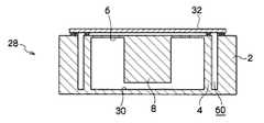
図1は本願発明の第1実施形態に係る加速度センサ1の斜視図であり、図2は実装状態における加速度センサ1のセンサ部28を図3に示す底面シリコン基板30に対して見下ろした平面図であり、図3は断面図である。 FIG. 1 is a perspective view of the acceleration sensor 1 according to the first embodiment of the present invention. FIG. 2 is a plan view of the
図1〜図3に示すように、加速度センサ1は、例えば平面視で一辺が数mm程度のほぼ正方形の略箱状とされ、底面シリコン基板30は後述するコントロールIC54に支持されている。加速度センサ1は、底面シリコン基板30上にセンサ部28を設けたたものであり、センサ部28は例えばSOI(silicon-on-insulator)ウエハに、エッチング等の処理を施して形成したものである。 As shown in FIGS. 1 to 3, the acceleration sensor 1 has, for example, a substantially square box shape with a side of about several mm in a plan view, and the
底面シリコン基板30上には平面視で略同形状をなす壁状の外枠2が設けられている。外枠2は例えばシリコンで形成され周囲を切れ目なく囲む壁であり、加速度センサ1の検出部分を周囲より遮蔽しセンサ部28を形成している。つまり外枠2は平面視で底面シリコン基板30と同様の形状(この場合は略正方形)をなす壁状の枠であり、内部に空間60を形成している。 On the
例えば図3に示す底面シリコン基板30の上に実装された加速度センサ1に対して、底面シリコン基板30に沿った方向(図中左右方向)からセンサ部28に対して印加される外力(物理的な押圧力など)を外枠2が受け止める構成とされており、センサ部28の内部構造を物理的に保護している。 For example, with respect to the acceleration sensor 1 mounted on the
図3に示すように、シリコン柱4は底面シリコン基板30から立設され、例えば図1、図2(A)に示すように外枠2からは所定の距離をあけて離間し、且つそれぞれが互いに離間して底面シリコン基板30の上に複数設けられている。 As shown in FIG. 3, the
シリコン柱4の先端からは、それぞれ底面シリコン基板30に沿う方向にビーム6が設けられ、複数のビーム6の先端は空間60の略中央付近で錘部8に一体的に形成されている。錘部8はビーム6によって底面シリコン基板30の上に間隙をあけて懸架されており、例えば加速度による慣性力を受けると図1に示すXYZいずれか、またはその組み合わせた方向にビーム6を歪ませる。
ビーム6にはピエゾ抵抗48が設けられており、上記のようにビーム6に歪みが加えられることにより、ピエゾ抵抗48の抵抗率が変化するピエゾ抵抗効果により、錘部8によって歪んだビーム6の歪みを電気抵抗の変化として検出する。 The
図2(A)に示すようにシリコン柱4の先端には例えばポリシリコンで形成された柱上接続パッド10が設けられ、配線50でピエゾ抵抗48に接続されている。柱上接続パッド10は例えばシリコン柱4の先端に形成された酸化膜上に設けられたポリシリコンパッドなどでよい。 As shown in FIG. 2A, a
同様に、外枠2の端面、すなわち底面シリコン基板30から遠い側の面には、例えばポリシリコンで形成された外枠上接続パッド12が設けられ、同じく外枠2の端面に形成されたボンディングパッド24に配線26で接続されている。ボンディングパッド24は加速度センサ1を外部で制御するコントロールICなどに接続される端子であり、配線26およびボンディングパッド24は例えば素子を形成する際にアルミ等で形成されていてもよい。 Similarly, on the end surface of the
図1、図2(A)に示すように、センサ部28の中においてはシリコン柱4は外枠2とは所定の距離をおいて離間しており、物理的に接触していないため、柱上接続パッド10から外枠2へピエゾ抵抗48で検出された電気抵抗値を伝達するための接続手段が設けられている。 As shown in FIGS. 1 and 2A, in the
すなわち、配線基板32には外枠上接続パッド12と接触する外側配線パッド14、および柱上接続パッド10と接触する内側配線パッド16とが設けられ、外側配線パッド14と内側配線パッド16とは配線38で接続されている。これにより、配線基板32をセンサ部28に接合することで柱上接続パッド10と外枠上接続パッド12とは電気的に接続される。 That is, the
図2(B)には底面シリコン基板30方向から見た配線基板32が示されている。配線基板32は底面シリコン基板30と対向するようにセンサ部28の外枠2に接合され、外枠2により形成された箱状構造の開口を封止する。 FIG. 2B shows the
配線基板32の内側配線パッド16は柱上接続パッド10(シリコン柱4)と、外側配線パッド14は外枠2の先端に設けられた外枠上接続パッド12(外枠2)とそれぞれ接触し、電気的に接続される。 The
また外枠2と配線基板32には、図2(A)(B)に示すように、それぞれ対向する面にセンサ側封止枠20と配線基板側封止枠22とが設けられている。外枠2のセンサ側封止枠20は例えばポリシリコン、配線基板側封止枠22は金薄膜などでもよい。 Further, as shown in FIGS. 2A and 2B, the
外枠2と配線基板32とが接合された際にはセンサ側封止枠20と配線基板側封止枠22とが互いに密着し、センサ部28の内側である空間60を外部から物理的に密閉、遮断する。 When the
図3にはセンサ部28の断面図が示されている。センサ部28は例えば酸化Siなどの絶縁膜上に単結晶シリコン層を形成した SOI(silicon-on-insulator)基板であってもよく、図3に示すようにセンサ部28の上に配線基板32が接合され、一体化した構造とされている。センサ部28と配線基板32の接合方法としては例えばAu−Si共晶接合等を用いることができる。同様に底面シリコン基板30とセンサ部28もまたAu−Si共晶接合等を用いて一体化した構造とすることができる。 FIG. 3 is a cross-sectional view of the
図4には加速度センサ1を制御するコントロールIC54上に加速度センサ1をマウントし、外部との電気的接続に用いられるリードフレーム52とボンディングワイヤ36で結線した構造が示されている。 FIG. 4 shows a structure in which the acceleration sensor 1 is mounted on a
すなわち、配線基板32と接合されたセンサ部28にはピエゾ抵抗48と接続されたボンディングパッド24が設けられており、コントロールIC54とボンディングワイヤ36で接続されている。コントロールIC54はリードフレーム52にマウントされ、ボンディングワイヤ36でリードフレーム52と結線される。これによりコントロールIC54はリードフレーム52を介して外部と電気的に接続される。 That is, a
また図4に示すようにコントロールIC54、リードフレーム52はボンディングワイヤ36等をも含めて封止樹脂34で封止され、最終的には全体として1個の樹脂部品としての形態を備える構造とされていてもよい。 Further, as shown in FIG. 4, the
<製造方法>
次に図8〜図10に沿って、加速度センサ1の製造方法について説明する。但し以下に説明する製造方法、素材、物性や寸法などはあくまでも一例であって、この方法に何等限定されるものではない。<Manufacturing method>
Next, a method for manufacturing the acceleration sensor 1 will be described with reference to FIGS. However, the manufacturing method, materials, physical properties, dimensions, and the like described below are merely examples, and the present invention is not limited to these methods.
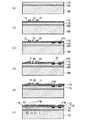
図2に示される加速度センサ1の、A−B断面を図8、図9に示す。図8はボンディングパッド24を含まない箇所の断面図、図9はボンディングパッド24を含む箇所の断面図である。先ず、図8(A)および図9(A)に示されるように、例えば工程1で厚さ525μmで体積抵抗率16Ω/cm程度のシリコン基板130に厚さ2μm程度の酸化シリコンによる埋め込み絶縁層120を介して厚さ5μmで体積抵抗率6〜8Ω/cm程度のN型のシリコン基板(活性層)110とで3層構造とされたSOIウエハを準備する。 FIGS. 8 and 9 show cross sections of the acceleration sensor 1 shown in FIG. FIG. 8 is a cross-sectional view of a portion not including the
次に、図8(B)および図9(B)に示されるように、工程2で、シリコン基板110の表面に、例えば1000℃程度の加湿雰囲気を用いた熱酸化条件で、厚さ0.4μm程度の酸化シリコンによる酸化膜(保護膜)172を形成する。 Next, as shown in FIGS. 8B and 9B, in
この酸化膜172上に、CVD(Chemical Vapor Deposition)法を用いてポリシリコンを成膜し、フォトリソグラフィーとエッチングにより柱上接続パッド10、外枠上接続パッド12、センサ側封止枠20をポリシリコンで形成する。 A polysilicon film is formed on the
次に、図8(C)および図9(C)に示されるように、工程3で、フォトリソエッチング技術を用いてレジストに開口部を設け酸化膜172を露出する。この酸化膜172を通してボロン拡散法により硼素をインプランテーションし、シリコン基板110(活性層)の表面にピエゾ抵抗48(図2参照)となるP型の拡散層174を形成する。レジスト剥離後にアニーリング(加熱応力除去)を行い、所望の拡散プロファイルを得る。 Next, as shown in FIGS. 8C and 9C, in step 3, an opening is formed in the resist using the photolithography etching technique to expose the
次いでピエゾ抵抗48とのコンタクト部分の酸化膜172をフォトリソグラフィーとエッチングにより開口する。 Next, the
次に、図8(D)および図9(D)に示されるように、工程4で、メタルスパッタリング技術を用いて酸化膜172上にアルミニウムを堆積し、アルミニウム層173を形成する。更に、フォトリソエッチング技術を用いてアルミニウム層173をエッチングし、ピエゾ抵抗48とのコンタクト部47、配線26およびボンディングパッド24となる部分を形成する。 Next, as shown in FIGS. 8D and 9D, in
次に、図8(E)および図9(D)に示されるように、工程5で、PRD(Plasma Reactive Deposition)法などを用いて、酸化膜172及びその上に形成された配線176の表面に、保護用のパッシベーション膜178を形成する。 Next, as shown in FIGS. 8E and 9D, in step 5, the surface of the
次に、図8(F)および図9(F)に示されるように、工程6で、パッシベーション膜178上にフォトレジストを形成し、フォトリソグラフィーとエッチングにより柱上接続パッド10、外枠上接続パッド12、センサ側封止枠20、およびボンディングパッド24となる部分を開口する。 Next, as shown in FIG. 8 (F) and FIG. 9 (F), in
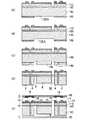
以下、図10ではSOIウエハの裏面からの加工について説明する。尚、図10の左半分はビーム6の存在する箇所(図2(A)のA−B断面)、右半分はシリコン柱4と錘部8とが繋がっていない箇所の断面を示す。 Hereinafter, processing from the back surface of the SOI wafer will be described with reference to FIG. Note that the left half of FIG. 10 shows a section where the
図10(A)に示されるように、工程7で、SOIウエハの裏面、即ちシリコン基板130の表面に、CVD技術を用いて酸化膜182を形成する。ここに錘部8となる部分を開口する。すなわち周囲の酸化膜182を残し、後に錘部8となる部分に相当する、中央部の酸化膜182をフォトリソエッチング技術を用いて除去して、開口部182Aを形成する。 As shown in FIG. 10A, in step 7, an
次に、図10(B)に示されるように、工程8で、周辺部に残された酸化膜182をエッチングマスクとし、D−RIE(いわゆるBosch法によるシリコン深堀技術法)を用いてシリコン基板130の表面を例えば20μm程度エッチングし、凹部130Aを形成する。これにより錘部8と底面シリコン基板30とが接触しない程度に錘部8が削られ、間隙が設けられる。 Next, as shown in FIG. 10B, in
次に、図10(C)に示されるように、工程9で、レジストを塗布しフォトリソ技術により、シリコン基板130のシリコン柱4と錘部8の間の隙間を形成するためのエッチングマスク186を形成する。 Next, as shown in FIG. 10C, in step 9, a resist is applied and an
次に、図10(D)に示されるように、工程10で、D−RIEを用いて、空間60を形成する Next, as shown in FIG. 10D, in
次に、図10(E)に示されるように、工程11で、工程10までの処理が完了したSOIウエハをD−RIEでエッチングし、シリコン基板110、130の間に形成されている絶縁層120をドライまたはウエットエッチングする。 Next, as shown in FIG. 10E, in step 11, the SOI wafer that has been processed up to step 10 is etched by D-RIE to form an insulating layer formed between the
次に、ここまでの工程で形成されたセンサ部28と、底面シリコン基板30とをAu−Si共晶結合によって接合する。
次に、再度SOIウエハの表面に戻り、レジストを塗布してフォトリソグラフィーで錘部8、外枠2、シリコン柱4、ビーム6以外の箇所を開口する。この開口部は、シリコン柱4と錘部8の間の隙間と一致する。この開口部にあるパッシベーション膜178と酸化膜172をドライまたはウエットでエッチングする。続いて、D-RIEにてシリコンを活性層の厚さ分エッチングする。ここで、先の工程10でエッチングした部分と貫通し、外枠2とシリコン柱4、錘部8等が分離される。最後にレジストを剥離してセンサ部28が完成する。
次に、底面シリコン基板30と接合したセンサ部28を配線基板32とAu−Si共晶結合によって接合する。これにより外枠2に配線基板32で蓋をした構造となる。Next, the
Next, returning to the surface of the SOI wafer again, a resist is applied, and portions other than the
Next, the
底面シリコン基板30の製造方法は例えば以下の通りである。まず、シリコン基板の表面にCrとAuをスパッタリングで成膜する。レジストを塗布し、外枠2およびシリコン柱4と接合される箇所を除いてレジストを開口する。開口部分のCrとAuをウエットエッチングで除去したのちレジストを剥離する。これにより外枠2およびシリコン柱4と接合される箇所のみCr膜とAu膜が残る。 The manufacturing method of the
上記のように底面シリコン基板30の接合面にはスパッタリング(又は蒸着)によって厚さ数μmのAu層が形成されている。これをAu−Si共晶温度363℃より高い温度(約400℃)の雰囲気中でAu層と他方のSi接合面とを重ねて数kg/平方cmから数十kg/平方cmの加重を印加することにより、Au−Si共晶結合を形成する。 As described above, an Au layer having a thickness of several μm is formed on the bonding surface of the
また配線基板32の製造方法は、例えば以下の通りである。まずシリコン基板上に酸化膜を形成し、配線18を拡散層配線として形成するために、フォトレジストをマスクとしてボロン拡散法により硼素をインプランテーションする。レジスト剥離後にアニーリング(加熱応力除去)を行い、所望の拡散プロファイルを得る。 Moreover, the manufacturing method of the
拡散層とのコンタクト部分にあたる箇所の酸化膜を、フォトリソグラフィーとエッチングにより開口する。スパッタリングにより基板の表面にCrとAuを成膜し、フォトリソグラフィーとエッチングにより外側配線パッド14、内側配線パッド16、配線基板側封止枠22部分を形成する。 An oxide film at a portion corresponding to a contact portion with the diffusion layer is opened by photolithography and etching. Cr and Au are formed on the surface of the substrate by sputtering, and the
次に、配線基板32の裏面にレジストを塗布し、ボンディングパッド部を露出する位置のレジストを開口する。このレジストをマスクにして、D-RIEを用いシリコンをエッチングすると、図2(B)のXのように開口部ができる。レジストを剥離して配線基板32が完成する。 Next, a resist is applied to the back surface of the
その後、通常の半導体製造方法と同様に、SOIウエハからチップを切り出し、例えばコントロールIC54上にマウントし、リードフレーム52上でボンディングワイヤ36で所定の配線を行ったのち、封止樹脂34で封止し、図4に示すように半導体チップとして形成される。 Thereafter, in the same manner as in a normal semiconductor manufacturing method, a chip is cut out from the SOI wafer, mounted on the
このとき外枠2と配線基板32とは、センサ側封止枠20、配線基板側封止枠22によって外部より遮断されているので、外枠2の内部に封止樹脂34が入り込むことはない。 At this time, since the
<作用効果>
本実施形態は上記構成としたので、以下のような優れた効果を有する。<Effect>
Since the present embodiment has the above configuration, it has the following excellent effects.
すなわち図2(B)に示されるように、加速度センサ1に加速度が加えられると、慣性力により錘部8に応力が作用し、錘部8が図1に示すX、Y、Zの何れか、あるいは組み合わせ方向に変位する。また、錘部8が変位すると、錘部8と接合されるビーム6が撓み、これより、ビーム6に取り付けられたピエゾ抵抗48の抵抗値が変化する。このピエゾ抵抗48の抵抗値変化を検出し、それに基づいて錘部8(加速度センサ1全体)に印加された加速度が検知される。 That is, as shown in FIG. 2 (B), when acceleration is applied to the acceleration sensor 1, stress is applied to the
このとき本実施形態において、図4に示すように加速度センサ1自体が封止樹脂34で封止されている構造では、封止樹脂34に印加される外部応力は外枠2が受け止める構成とされている。 At this time, in this embodiment, in the structure in which the acceleration sensor 1 itself is sealed with the sealing
すなわち封止樹脂34に印加される外部応力は外枠2が受け止め、外枠2とは間隙を設けて分離されたシリコン柱4、およびシリコン柱4から延設され錘部8を保持しているビーム6に対しては外部応力が直接伝わることはない。 That is, the
このため、ビーム6の変位を計測することで測定される加速度データに対して、外部応力が影響する虞はなく、また外をゲル剤等でカバーする工程も不要となるので、工数およびコスト、時間を削減することができる。 For this reason, there is no possibility that external stress may affect the acceleration data measured by measuring the displacement of the
<第2実施形態>
図5、図6には本願発明の第2実施形態に係る加速度センサの構造が示されている。本願発明の第2実施形態に係る加速度センサ101は、いわゆるWCSPと呼ばれるパッケージの形態であり、ウエハーの状態で再配線や保護膜、端子の形成を行い、その後に個片化したパッケージを示す。Second Embodiment
5 and 6 show the structure of the acceleration sensor according to the second embodiment of the present invention. The
WCSPはパッケージの実装面積が半導体チップと同じ大きさになり、リードフレームに搭載する必要がなく、ウエハーを個片化してから樹脂などでモールドして端子などを形成する第1実施形態に比べて小型になる特長を備えている。さらに、ボンディングパッドを経由せず直接、配線基板に設けられたCuポスト(半田ボール)にて基板との接続が行われるため、より実装面積を小さくできる。 WCSP has the same package mounting area as a semiconductor chip, and does not need to be mounted on a lead frame. Compared to the first embodiment in which a wafer is separated into individual pieces and then molded with resin or the like to form terminals. It has the feature of being small. Furthermore, since the connection to the substrate is made directly by Cu posts (solder balls) provided on the wiring substrate without going through the bonding pads, the mounting area can be further reduced.
また第1実施形態と比較すると、ウエハ上に形成されたセンサをダイシングで切断、個別に分離することでプロセスは終了するため、パッケージングプロセスの全てがウェハー状態で完結する事を特徴としている。 Compared with the first embodiment, the process is completed by cutting and individually separating the sensors formed on the wafer by dicing, so that the entire packaging process is completed in the wafer state.
図5、図6に示すように、本願発明の第2実施形態に係る加速度センサ101は第1実施形態と同様、外枠2とシリコン柱4とが間隙を設けて分離された構造とされているが、第1実施形態とは異なり、ボンディングパッド24にてセンサ外部へ信号を伝達することなく、配線基板32の外側面に設けられたCuポストを接続端子とすることにより、リードフレーム52を介することなく、直接基板などに実装される構造とされている。さらに封止樹脂34を用いず、外枠2で囲われた箱構造がセンサ自体の外形を成している。この実施形態の配線基板32には、ボンディングパッド部のシリコンエッチングは施さないものとする。 As shown in FIGS. 5 and 6, the
これにより外枠2に設けられるセンサ側封止枠20と配線基板32に設けられる配線基板側封止枠22とは、それぞれ図5で示す平面図では最外周に設けられている。 Thereby, the sensor
この結果、図6(B)に示すように外枠2と配線基板32とが接合されると、それぞれの最外周に設けられたセンサ側封止枠20と配線基板側封止枠22とが接合され、外枠2の内部すなわち加速度センサ101の検知部分を封止する。 As a result, when the
また、外枠2の上面に設けられた外枠上接続パッド12は外部への電気的接続は行わないが、外枠2と配線基板32との間隔を維持し、配線基板32側の外側配線パッド14と接触する高さをシリコン柱4上の柱上接続パッド10と等しい高さに保つスペーサとして機能する。 In addition, the outer
いわゆるWCSP(Wafer-Level Chip Size Package)構造とされた本実施形態においては、封止樹脂を用いるパッケージに比較して加速度センサ自体の小型化、低背化が可能であり、実装における自由度が向上し、高集積化も可能となる。また部品点数および組立工数の削減によりコスト・時間の削減が可能となる。 In the present embodiment having a so-called WCSP (Wafer-Level Chip Size Package) structure, the acceleration sensor itself can be reduced in size and height compared to a package using a sealing resin, and the degree of freedom in mounting is increased. This improves the integration density. In addition, cost and time can be reduced by reducing the number of parts and the number of assembly steps.
<製造方法>
次に加速度センサ101の製造方法について説明する。但し以下に説明する製造方法、素材、物性や寸法などはあくまでも一例であって、この方法に何等限定されるものではない。また第1実施形態と共通する工程に関しては、これを省略する。<Manufacturing method>
Next, a method for manufacturing the
第1実施形態と同様、図11(A)に示すようなシリコンウエハ140上に、第1実施形態と同様、図11(B)に示すように外枠2、シリコン柱4、ビーム6などを形成する。 Similar to the first embodiment, on the
図11(C)に示すようにセンサ部28側のプロセスを終えた時点で第1実施形態と同様に外枠2で覆われたセンサ部28がシリコンウエハ上に形成されており、これに配線基板32を貼り合わせることで外枠2の開口を封止する点までは第1実施形態と同様である。 As shown in FIG. 11C, when the process on the
ここで用いられる配線基板32の製造方法は第1実施形態と異なり、まずシリコン基板上に熱酸化処理にて酸化シリコンによる酸化膜を形成する。この上にCrとAuとをスパッタリング処理にて成膜する。 The manufacturing method of the
次に、これをフォトリソグラフィーとエッチングにより図6(B)に示すように外枠上接続パッド12と接触する外側配線パッド14、および柱上接続パッド10と接触する内側配線パッド16、外側配線パッド14と内側配線パッド16を接続する配線38を形成する。 Next, by photolithography and etching, as shown in FIG. 6B, the
次に、図11(C)に示すように、底面シリコン基板をAu−Si共晶接合により貼り合わせたセンサ部28に対して、上記の配線基板32をAu−Si共晶接合にて貼り合わせる。 Next, as shown in FIG. 11C, the
次に、図11(D)に示すように配線基板32の外側面にレジストを塗布したのち貫通電極(Cuポスト40)を設ける箇所をD-RIEを用いてシリコンをエッチングし、その下の酸化膜もエッチングし貫通させる。この貫通穴側壁を酸化膜で絶縁し、配線基板32を貫通するようにCuポスト40を形成する。 Next, as shown in FIG. 11D, after applying a resist to the outer surface of the
さらに外側面にエポキシ樹脂などを積層して保護層44とし、フォトリソグラフィーでCuポスト40上の部分を開口し、再配線後にCuポスト42を形成する。さらにCuポスト42上に半田ボール46を形成し、ボンディングパッドのかわりとする。 Further, an epoxy resin or the like is laminated on the outer surface to form a
次に、図11(E)に示すように個々のセンサ部28をダイシングにより切り分け、分離する。これによりセンサ部28はそれぞれが個々に加速度センサ101として形成される。 Next, as shown in FIG. 11E, the
完成した加速度センサ101は、例えば図11(F)に示すように半田ボール46を外部との接続端子とする加速度センサユニットであり、外枠2にて周囲を囲われると共に、図6(B)に示すようにセンサ側封止枠20と配線基板側封止枠22とが接合され、外枠2の内部すなわち加速度センサ101の検知部分を封止する。 The completed
前述のように加速度センサ101は封止樹脂による外部からの封止を行う必要はなく、また外枠2とシリコン柱4とは分離しているので、加速度センサ101に印加された外部応力がビーム6に伝達され測定精度に影響を与える虞はない。 As described above, the
<第3実施形態>
図7には本願発明の第3実施形態に係る加速度センサの構造が示されている。図7に示すように、本願発明の第3実施形態に係る加速度センサ102は例えば第1実施形態と同様、ビーム6に設けられたピエゾ抵抗48と電気的に接続される外枠上接続パッド12から、外枠2上に設けられたボンディングパッド24へ配線26で接続されている。<Third Embodiment>
FIG. 7 shows the structure of an acceleration sensor according to the third embodiment of the present invention. As shown in FIG. 7, the
このときボンディングパッド24、およびボンディングパッド24に至る配線26は外枠2上では自由に配置できるため、図7(A)のように一方向にボンディングパッド24を集結させた構成とされていてもよい。 At this time, since the
この構成では、ボンディングパッド24を加速度センサ102の片側の一辺に集結させて配置したことにより、片側の一辺からワイヤ接続を行うことができ、基板等に実装する際にワイヤを四方に引き回す必要がなくなるため、第1実施形態の配置と合わせて実装時の自由度を大きくすることができる。このとき図7(B)に示すように、配線基板32の形状、部品配置は第1実施形態と同様なので、共通部品として用いることができる。 In this configuration, since the
<まとめ>
以上、本発明の実施例について記述したが、本発明は上記の実施例に何ら限定されるものではなく、本発明の要旨を逸脱しない範囲において種々なる態様で実施し得ることは言うまでもない。<Summary>
As mentioned above, although the Example of this invention was described, it cannot be overemphasized that this invention is not limited to said Example at all, and can implement in a various aspect in the range which does not deviate from the summary of this invention.
例えば本発明は加速度センサに関するものであるが、これ以外にも外部応力を遮断する目的で外枠を設ける素子構造に応用することもできる。すなわち、例えば検出・駆動電極を最上層と最下層基板とに分散して配置した3層構造の静電容量型角速度センサ等の用途にも本発明を応用することができる。この場合、中間層として錘を支持する梁部材に外部応力が伝達されることを防止し、測定精度への影響を防ぐことができる。 For example, the present invention relates to an acceleration sensor, but can also be applied to an element structure in which an outer frame is provided for the purpose of blocking external stress. That is, for example, the present invention can also be applied to uses such as a three-layered capacitive angular velocity sensor in which detection / drive electrodes are dispersed and arranged on the uppermost layer and the lowermost substrate. In this case, it is possible to prevent external stress from being transmitted to the beam member that supports the weight as the intermediate layer, and to prevent influence on the measurement accuracy.
1 加速度センサ
2 外枠
4 シリコン柱
6 ビーム
8 錘部
10 柱上接続パッド
12 外枠上接続パッド
14 外側配線パッド
16 内側配線パッド
18 配線
20 センサ側封止枠
22 配線基板側封止枠
24 ボンディングパッド
26 配線
28 センサ部
30 底面シリコン基板
32 配線基板
34 封止樹脂
36 ボンディングワイヤ
38 配線
40 ポスト
42 ポスト
44 保護層
46 半田ボール
48 ピエゾ抵抗
50 リードフレーム
54 コントロールIC
60 空間
101 加速度センサ
102 加速度センサDESCRIPTION OF SYMBOLS 1
60
Claims (5)
Translated fromJapanese前記錘部の周囲で底板上に形成された複数の固定部と、
前記固定部と前記錘部に連結され、前記錘部を前記底板から離間した位置に保持する梁部と、
前記梁部に設けられ、前記梁部の変形を検出する検出部と、
前記底板から立設されると共に前記固定部から離間した位置でこれを囲む枠部と、
前記枠部の開口を封止する板状の蓋部と、
前記固定部の端部に設けられ、前記検出部より電気信号を伝達される固定部接続パッドと、
前記蓋部の内側面に設けられ、前記固定部接続パッドと接触する第1の蓋部接続パッドと、
前記蓋部の内側面に設けられ、前記第1の蓋部接続パッドと配線で接続される第2の蓋部接続パッドと、
前記枠部に設けられ、前記第2の蓋部接続パッドと接触する枠部接続パッドと、
前記蓋部と接触しないように前記枠部に設けられ、前記枠部接続パッドと配線で接続され電気信号を外部へ伝達するボンディングパッドと、
を備え、
前記蓋部に対向する前記梁部の面と、前記蓋部に対向する前記固定部の面が面一であることを特徴とする加速度センサ。A weight part;
A plurality of fixing parts formed on the bottom plate around the weight part;
A beam portion connected to the fixed portion and the weight portion, and holding the weight portion at a position separated from the bottom plate;
A detection unit provided in the beam unit for detecting deformation of the beam unit;
A frame that stands upright from the bottom plate and surrounds it at a position spaced from the fixed portion;
A plate-like lid portion for sealing the opening of the frame portion;
A fixed portion connection pad provided at an end portion of the fixed portion, to which an electric signal is transmitted from the detection portion ;
A first lid connection pad provided on an inner surface of the lid and in contact with the fixed part connection pad ;
A second lid connecting pad provided on an inner surface of the lid and connected to the first lid connecting pad by wiring ;
A frame connection pad provided on the frame and in contact with the second lid connection pad ;
A bonding pad provided on the frame portion so as not to contact the lid portion, connected to the frame portion connection pad by wiring and transmitting an electrical signal to the outside ;
With
An acceleration sensor characterized in that asurface of the beam portion facing the lid portion and a surface of the fixing portion facing the lid portion are flush with each other.
Priority Applications (2)
| Application Number | Priority Date | Filing Date | Title |
|---|---|---|---|
| JP2009262104AJP5486271B2 (en) | 2009-11-17 | 2009-11-17 | Acceleration sensor and method of manufacturing acceleration sensor |
| US12/942,130US8522613B2 (en) | 2009-11-17 | 2010-11-09 | Acceleration sensor |
Applications Claiming Priority (1)
| Application Number | Priority Date | Filing Date | Title |
|---|---|---|---|
| JP2009262104AJP5486271B2 (en) | 2009-11-17 | 2009-11-17 | Acceleration sensor and method of manufacturing acceleration sensor |
Publications (2)
| Publication Number | Publication Date |
|---|---|
| JP2011106955A JP2011106955A (en) | 2011-06-02 |
| JP5486271B2true JP5486271B2 (en) | 2014-05-07 |
Family
ID=44010301
Family Applications (1)
| Application Number | Title | Priority Date | Filing Date |
|---|---|---|---|
| JP2009262104AExpired - Fee RelatedJP5486271B2 (en) | 2009-11-17 | 2009-11-17 | Acceleration sensor and method of manufacturing acceleration sensor |
Country Status (2)
| Country | Link |
|---|---|
| US (1) | US8522613B2 (en) |
| JP (1) | JP5486271B2 (en) |
Families Citing this family (21)
| Publication number | Priority date | Publication date | Assignee | Title |
|---|---|---|---|---|
| TWI461692B (en)* | 2011-12-01 | 2014-11-21 | Nat Univ Tsing Hua | A inertial sensor with stress isolation structure |
| JP2013171009A (en)* | 2012-02-23 | 2013-09-02 | Hitachi Automotive Systems Ltd | Inertial force sensor |
| DE102012206719A1 (en)* | 2012-04-24 | 2013-10-24 | Robert Bosch Gmbh | Micromechanical sensor element and sensor device with such a sensor element |
| CN104797943A (en)* | 2012-11-19 | 2015-07-22 | 株式会社村田制作所 | Angular acceleration sensor |
| CN105308463A (en)* | 2013-06-04 | 2016-02-03 | 株式会社村田制作所 | Acceleration sensor |
| EP3094950B1 (en)* | 2014-01-13 | 2022-12-21 | Nextinput, Inc. | Miniaturized and ruggedized wafer level mems force sensors |
| KR20150085705A (en)* | 2014-01-16 | 2015-07-24 | 삼성전기주식회사 | Acceleration Sensor |
| CN107848788B (en) | 2015-06-10 | 2023-11-24 | 触控解决方案股份有限公司 | Ruggedized wafer-level MEMS force sensor with tolerance trench |
| US11243125B2 (en) | 2017-02-09 | 2022-02-08 | Nextinput, Inc. | Integrated piezoresistive and piezoelectric fusion force sensor |
| EP3580539A4 (en) | 2017-02-09 | 2020-11-25 | Nextinput, Inc. | INTEGRATED DIGITAL FORCE SENSORS AND RELATED METHOD OF MANUFACTURING |
| US11221263B2 (en) | 2017-07-19 | 2022-01-11 | Nextinput, Inc. | Microelectromechanical force sensor having a strain transfer layer arranged on the sensor die |
| WO2019023309A1 (en) | 2017-07-25 | 2019-01-31 | Nextinput, Inc. | Integrated fingerprint and force sensor |
| WO2019023552A1 (en) | 2017-07-27 | 2019-01-31 | Nextinput, Inc. | A wafer bonded piezoresistive and piezoelectric force sensor and related methods of manufacture |
| WO2019079420A1 (en) | 2017-10-17 | 2019-04-25 | Nextinput, Inc. | Temperature coefficient of offset compensation for force sensor and strain gauge |
| WO2019090057A1 (en) | 2017-11-02 | 2019-05-09 | Nextinput, Inc. | Sealed force sensor with etch stop layer |
| WO2019099821A1 (en) | 2017-11-16 | 2019-05-23 | Nextinput, Inc. | Force attenuator for force sensor |
| CN109406826A (en)* | 2018-08-30 | 2019-03-01 | 南京理工大学 | Accelerometer installation method based on rotary motion body |
| US10962427B2 (en) | 2019-01-10 | 2021-03-30 | Nextinput, Inc. | Slotted MEMS force sensor |
| JP7452383B2 (en)* | 2020-11-06 | 2024-03-19 | 株式会社デンソー | Manufacturing method of multi-axis inertial force sensor |
| CN113390552B (en)* | 2021-06-11 | 2025-07-11 | 深圳市美思先端电子有限公司 | A pressure sensor and a method for manufacturing the same |
| KR102505956B1 (en)* | 2021-10-14 | 2023-03-03 | 국방과학연구소 | Accelerometer |
Family Cites Families (14)
| Publication number | Priority date | Publication date | Assignee | Title |
|---|---|---|---|---|
| JPH07280679A (en) | 1994-04-06 | 1995-10-27 | Hokuriku Electric Ind Co Ltd | Pressure sensor |
| JP2000187040A (en) | 1998-12-22 | 2000-07-04 | Matsushita Electric Works Ltd | Acceleration sensor and its manufacture |
| JP2003270263A (en)* | 2002-03-19 | 2003-09-25 | Matsushita Electric Works Ltd | Semiconductor acceleration sensor |
| US6892578B2 (en)* | 2002-11-29 | 2005-05-17 | Hitachi Metals Ltd. | Acceleration sensor |
| JP2006214963A (en)* | 2005-02-07 | 2006-08-17 | Seiko Instruments Inc | Acceleration sensor, electronic equipment, and manufacturing method for acceleration sensor |
| JP2006250550A (en)* | 2005-03-08 | 2006-09-21 | Omron Corp | Sensor |
| JP5095930B2 (en)* | 2005-08-12 | 2012-12-12 | パナソニック株式会社 | MEMS device and manufacturing method thereof |
| JP3938198B1 (en)* | 2005-12-22 | 2007-06-27 | 松下電工株式会社 | Wafer level package structure and sensor element |
| JP2008026183A (en) | 2006-07-21 | 2008-02-07 | Mitsumi Electric Co Ltd | Ic-integrated acceleration sensor |
| US7640805B2 (en)* | 2006-12-18 | 2010-01-05 | Akustica, Inc. | Proof-mass with supporting structure on integrated circuit-MEMS platform |
| JP2008170271A (en) | 2007-01-11 | 2008-07-24 | Murata Mfg Co Ltd | External force detection sensor |
| JP5475946B2 (en)* | 2007-11-21 | 2014-04-16 | パナソニック株式会社 | Sensor module |
| JP2009241164A (en)* | 2008-03-28 | 2009-10-22 | Torex Semiconductor Ltd | Semiconductor sensor apparatus and manufacturing method therefor |
| JP2010107394A (en)* | 2008-10-30 | 2010-05-13 | Kyocera Corp | Acceleration sensor element and device |
- 2009
- 2009-11-17JPJP2009262104Apatent/JP5486271B2/ennot_activeExpired - Fee Related
- 2010
- 2010-11-09USUS12/942,130patent/US8522613B2/ennot_activeExpired - Fee Related
Also Published As
| Publication number | Publication date |
|---|---|
| US8522613B2 (en) | 2013-09-03 |
| US20110113881A1 (en) | 2011-05-19 |
| JP2011106955A (en) | 2011-06-02 |
Similar Documents
| Publication | Publication Date | Title |
|---|---|---|
| JP5486271B2 (en) | Acceleration sensor and method of manufacturing acceleration sensor | |
| US10816422B2 (en) | Pressure sensor | |
| CN101900746B (en) | Acceleration sensor element and acceleration sensor having same | |
| US7674638B2 (en) | Sensor device and production method therefor | |
| US8067769B2 (en) | Wafer level package structure, and sensor device obtained from the same package structure | |
| EP3076146B1 (en) | Pressure sensor | |
| JP2008020433A (en) | Mechanical mass sensor | |
| JP2005249454A (en) | Capacitive acceleration sensor | |
| JP2007240250A (en) | Pressure sensor, pressure sensor package, pressure sensor module, and electronic component | |
| JP4968371B2 (en) | Manufacturing method of sensor device and sensor device | |
| JP4925275B2 (en) | Semiconductor device | |
| JP2007263766A (en) | Sensor device | |
| JP3938199B1 (en) | Wafer level package structure and sensor device | |
| JP4706634B2 (en) | Semiconductor sensor and manufacturing method thereof | |
| JP2010008172A (en) | Semiconductor device | |
| JP5118923B2 (en) | Semiconductor device | |
| JP4949673B2 (en) | Semiconductor acceleration sensor and manufacturing method thereof | |
| JP4925273B2 (en) | Semiconductor device | |
| JP5328492B2 (en) | Pressure sensor module, pressure sensor package, and manufacturing method thereof | |
| JP2009047650A (en) | Sensor device and manufacturing method thereof | |
| JP2007263767A (en) | Sensor device | |
| JP3938200B1 (en) | Sensor device and manufacturing method thereof | |
| JP2006214963A (en) | Acceleration sensor, electronic equipment, and manufacturing method for acceleration sensor | |
| JP5328479B2 (en) | Pressure sensor module, pressure sensor package, and manufacturing method thereof | |
| WO2009119840A1 (en) | Acceleration sensor element, acceleration sensor device and method for manufacturing acceleration sensor element |
Legal Events
| Date | Code | Title | Description |
|---|---|---|---|
| A621 | Written request for application examination | Free format text:JAPANESE INTERMEDIATE CODE: A621 Effective date:20121101 | |
| A977 | Report on retrieval | Free format text:JAPANESE INTERMEDIATE CODE: A971007 Effective date:20130614 | |
| A131 | Notification of reasons for refusal | Free format text:JAPANESE INTERMEDIATE CODE: A131 Effective date:20130618 | |
| A521 | Request for written amendment filed | Free format text:JAPANESE INTERMEDIATE CODE: A523 Effective date:20130813 | |
| A977 | Report on retrieval | Free format text:JAPANESE INTERMEDIATE CODE: A971007 Effective date:20130829 | |
| TRDD | Decision of grant or rejection written | ||
| A01 | Written decision to grant a patent or to grant a registration (utility model) | Free format text:JAPANESE INTERMEDIATE CODE: A01 Effective date:20140204 | |
| A61 | First payment of annual fees (during grant procedure) | Free format text:JAPANESE INTERMEDIATE CODE: A61 Effective date:20140221 | |
| R150 | Certificate of patent or registration of utility model | Ref document number:5486271 Country of ref document:JP Free format text:JAPANESE INTERMEDIATE CODE: R150 | |
| LAPS | Cancellation because of no payment of annual fees |