JP5484741B2 - Semiconductor device - Google Patents
Semiconductor deviceDownload PDFInfo
- Publication number
- JP5484741B2 JP5484741B2JP2009012610AJP2009012610AJP5484741B2JP 5484741 B2JP5484741 B2JP 5484741B2JP 2009012610 AJP2009012610 AJP 2009012610AJP 2009012610 AJP2009012610 AJP 2009012610AJP 5484741 B2JP5484741 B2JP 5484741B2
- Authority
- JP
- Japan
- Prior art keywords
- semiconductor
- semiconductor region
- region
- depth
- semiconductor substrate
- Prior art date
- Legal status (The legal status is an assumption and is not a legal conclusion. Google has not performed a legal analysis and makes no representation as to the accuracy of the status listed.)
- Active
Links
Images


Classifications
- H—ELECTRICITY
- H10—SEMICONDUCTOR DEVICES; ELECTRIC SOLID-STATE DEVICES NOT OTHERWISE PROVIDED FOR
- H10D—INORGANIC ELECTRIC SEMICONDUCTOR DEVICES
- H10D30/00—Field-effect transistors [FET]
- H10D30/60—Insulated-gate field-effect transistors [IGFET]
- H10D30/64—Double-diffused metal-oxide semiconductor [DMOS] FETs
- H10D30/66—Vertical DMOS [VDMOS] FETs
- H—ELECTRICITY
- H10—SEMICONDUCTOR DEVICES; ELECTRIC SOLID-STATE DEVICES NOT OTHERWISE PROVIDED FOR
- H10D—INORGANIC ELECTRIC SEMICONDUCTOR DEVICES
- H10D12/00—Bipolar devices controlled by the field effect, e.g. insulated-gate bipolar transistors [IGBT]
- H10D12/411—Insulated-gate bipolar transistors [IGBT]
- H10D12/441—Vertical IGBTs
- H10D12/461—Vertical IGBTs having non-planar surfaces, e.g. having trenches, recesses or pillars in the surfaces of the emitter, base or collector regions
- H10D12/481—Vertical IGBTs having non-planar surfaces, e.g. having trenches, recesses or pillars in the surfaces of the emitter, base or collector regions having gate structures on slanted surfaces, on vertical surfaces, or in grooves, e.g. trench gate IGBTs
- H—ELECTRICITY
- H10—SEMICONDUCTOR DEVICES; ELECTRIC SOLID-STATE DEVICES NOT OTHERWISE PROVIDED FOR
- H10D—INORGANIC ELECTRIC SEMICONDUCTOR DEVICES
- H10D30/00—Field-effect transistors [FET]
- H10D30/01—Manufacture or treatment
- H10D30/021—Manufacture or treatment of FETs having insulated gates [IGFET]
- H10D30/028—Manufacture or treatment of FETs having insulated gates [IGFET] of double-diffused metal oxide semiconductor [DMOS] FETs
- H10D30/0291—Manufacture or treatment of FETs having insulated gates [IGFET] of double-diffused metal oxide semiconductor [DMOS] FETs of vertical DMOS [VDMOS] FETs
- H—ELECTRICITY
- H10—SEMICONDUCTOR DEVICES; ELECTRIC SOLID-STATE DEVICES NOT OTHERWISE PROVIDED FOR
- H10D—INORGANIC ELECTRIC SEMICONDUCTOR DEVICES
- H10D62/00—Semiconductor bodies, or regions thereof, of devices having potential barriers
- H10D62/10—Shapes, relative sizes or dispositions of the regions of the semiconductor bodies; Shapes of the semiconductor bodies
- H10D62/102—Constructional design considerations for preventing surface leakage or controlling electric field concentration
- H10D62/103—Constructional design considerations for preventing surface leakage or controlling electric field concentration for increasing or controlling the breakdown voltage of reverse-biased devices
- H10D62/105—Constructional design considerations for preventing surface leakage or controlling electric field concentration for increasing or controlling the breakdown voltage of reverse-biased devices by having particular doping profiles, shapes or arrangements of PN junctions; by having supplementary regions, e.g. junction termination extension [JTE]
- H10D62/109—Reduced surface field [RESURF] PN junction structures
- H10D62/111—Multiple RESURF structures, e.g. double RESURF or 3D-RESURF structures
- H—ELECTRICITY
- H10—SEMICONDUCTOR DEVICES; ELECTRIC SOLID-STATE DEVICES NOT OTHERWISE PROVIDED FOR
- H10D—INORGANIC ELECTRIC SEMICONDUCTOR DEVICES
- H10D62/00—Semiconductor bodies, or regions thereof, of devices having potential barriers
- H10D62/10—Shapes, relative sizes or dispositions of the regions of the semiconductor bodies; Shapes of the semiconductor bodies
- H10D62/17—Semiconductor regions connected to electrodes not carrying current to be rectified, amplified or switched, e.g. channel regions
- H10D62/393—Body regions of DMOS transistors or IGBTs
Landscapes
- Insulated Gate Type Field-Effect Transistor (AREA)
Description
Translated fromJapanese本発明は、半導体装置に関し、特に、各種のスイッチング電源に代表されるパワーエレクトロニクス分野に応用されるパワー半導体装置に関する。 The present invention relates to a semiconductor device, and more particularly to a power semiconductor device applied to the field of power electronics represented by various switching power supplies.
MOS型電界効果トランジスタ(以下、「MOSFET」という)や絶縁ゲート型バイポーラ・トランジスタ(以下、「IGBT」という)などの半導体装置は、高速スイッチング特性及び数10〜数100Vの逆方向阻止電圧(以下、「耐圧」という)を有している。したがって、これらの半導体装置は、家庭用電気機器、通信機器、及び車載用モータ等の電力変換のような制御分野に広く用いられている。これらの半導体装置を用いた電源システムの小型化、高効率化、及び低消費電力化を達成するためには、システムを構成する半導体装置のオン状態での抵抗(以下、「オン抵抗」という)を低減する必要がある。すなわち、MOSFETやIGBTは、高耐圧及び低オン抵抗が強く要求されている。 Semiconductor devices such as MOS field effect transistors (hereinafter referred to as “MOSFETs”) and insulated gate bipolar transistors (hereinafter referred to as “IGBTs”) have high-speed switching characteristics and a reverse blocking voltage (hereinafter referred to as several tens to several hundreds volts). , "Withstand voltage"). Therefore, these semiconductor devices are widely used in the field of control such as power conversion for household electric devices, communication devices, and in-vehicle motors. In order to achieve miniaturization, high efficiency, and low power consumption of a power supply system using these semiconductor devices, the resistance of the semiconductor devices constituting the system in the on state (hereinafter referred to as “on resistance”). Need to be reduced. That is, MOSFETs and IGBTs are strongly required to have high breakdown voltage and low on-resistance.
一般的には、半導体装置は、オフ状態で高電圧が印加されると、ドリフト領域が空乏化して電圧を保持する。MOSFETやIGBTなどの半導体装置は、高耐圧を得るために不純物濃度が比較的低いドリフト領域を有するので、抵抗が大きくなり、素子のオン抵抗に占めるドリフト抵抗の割合が増大し、結果として、オン抵抗も大きくなる。したがって、これらの半導体装置では、耐圧とオン抵抗とがトレードオフの関係を有し、その材料で決定される限界が存在する。 Generally, in a semiconductor device, when a high voltage is applied in an off state, the drift region is depleted and the voltage is held. Semiconductor devices such as MOSFETs and IGBTs have a drift region with a relatively low impurity concentration in order to obtain a high breakdown voltage, so that the resistance increases and the ratio of the drift resistance to the on-resistance of the element increases. Resistance also increases. Therefore, in these semiconductor devices, the breakdown voltage and the on-resistance have a trade-off relationship, and there is a limit determined by the material.
これに対して、このドリフト抵抗を低減するための構造として、スーパージャンクション構造が知られている(非特許文献1を参照)。このスーパージャンクション構造とは、ドリフト領域において電流経路に対して垂直方向にp型半導体層とn型半導体層とが交互に配置された構造である。 On the other hand, a super junction structure is known as a structure for reducing the drift resistance (see Non-Patent Document 1). The super junction structure is a structure in which p-type semiconductor layers and n-type semiconductor layers are alternately arranged in a direction perpendicular to the current path in the drift region.
一般的な半導体装置では、ドレイン電極に高電圧が印加されると、ソース電極に接続されているp型ベース領域とn型ドリフト領域とのpn接合面より空乏層が広がるので、このpn接合面の電界の強度が臨界電界に達したときにアバランシェ降伏が起こる。したがって、一般的な半導体装置の耐圧は、n型ドリフト領域の不純物濃度及び空乏層距離によって決定される。 In a general semiconductor device, when a high voltage is applied to the drain electrode, a depletion layer spreads from the pn junction surface between the p-type base region and the n-type drift region connected to the source electrode. The avalanche breakdown occurs when the intensity of the electric field reaches a critical electric field. Therefore, the breakdown voltage of a general semiconductor device is determined by the impurity concentration and the depletion layer distance in the n-type drift region.
これに対して、スーパージャンクション構造では、n型ドリフト領域とのpn接合面に加えて、ドリフト領域におけるp型半導体層とn型半導体層とのpn接合からも空乏層が広がる。したがって、p型ベース領域とn型ドリフト領域とのpn接合面のみへの電界集中が緩和され、ドリフト領域全体の電界が上昇し、結果として、n型半導体層の不純物濃度を通常の半導体装置のドリフト領域よりも高濃度化した場合であっても高耐圧が得られる。さらに、半導体装置のオン状態では、電流が高濃度のn型半導体層を流れるので、同程度の耐圧を有する一般的な半導体装置と比較して、オン抵抗を1/5程度にすることができる。 On the other hand, in the super junction structure, the depletion layer extends from the pn junction between the p-type semiconductor layer and the n-type semiconductor layer in the drift region in addition to the pn junction surface with the n-type drift region. Therefore, the electric field concentration only on the pn junction surface between the p-type base region and the n-type drift region is relaxed, and the electric field of the entire drift region is increased. As a result, the impurity concentration of the n-type semiconductor layer is reduced to that of a normal semiconductor device. Even when the concentration is higher than that of the drift region, a high breakdown voltage can be obtained. Further, since the current flows through the n-type semiconductor layer with a high concentration in the on state of the semiconductor device, the on-resistance can be reduced to about 1/5 as compared with a general semiconductor device having the same breakdown voltage. .
しかしながら、スーパージャンクション構造に対しても、さらなるオン抵抗の低減が求められている。スーパージャンクション構造のオン抵抗をより低減するためには、n型半導体層の不純物濃度を上げる必要がある。この場合には、耐圧を保持するためにn型半導体層を空乏化しなくてはならないので、n型半導体層とp型半導体層の幅を狭くする必要がある。すなわち、それぞれの半導体層のアスペクト比を増加させる必要がある。 However, a further reduction in on-resistance is also required for the super junction structure. In order to further reduce the on-resistance of the super junction structure, it is necessary to increase the impurity concentration of the n-type semiconductor layer. In this case, since the n-type semiconductor layer must be depleted in order to maintain the breakdown voltage, it is necessary to narrow the widths of the n-type semiconductor layer and the p-type semiconductor layer. That is, it is necessary to increase the aspect ratio of each semiconductor layer.
ここで、スーパージャンクション構造を形成するためのプロセスとして、n型エピタキシャル層表面よりリアクティブ・イオン・エッチング(以下、「RIE」という)でトレンチを形成して、p型層をエピタキシャル成長させる方法(特許文献1を参照)や、高抵抗のエピタキシャル層にn型及びp型の埋め込み層をイオン注入及び拡散によって選択的に形成し、高抵抗のエピタキシャル層を積み増しし、下層と同様にn型及びp型の埋め込み層をイオン注入及び拡散によって形成させる工程を複数回繰り返す製造方法(特許文献2を参照)が知られている。 Here, as a process for forming a super junction structure, a p-type layer is epitaxially grown by forming a trench by reactive ion etching (hereinafter referred to as “RIE”) from the surface of an n-type epitaxial layer (patent) Reference 1), n-type and p-type buried layers are selectively formed in the high-resistance epitaxial layer by ion implantation and diffusion, and the high-resistance epitaxial layers are stacked. There is known a manufacturing method (see Patent Document 2) in which a step of forming a buried layer of a mold by ion implantation and diffusion is repeated a plurality of times.
特許文献1に開示されている方法は、高アスペクト比でトレンチ内部に良質なシリコンをエピタキシャル成長させ、不純物濃度等を高い制御性で埋め込むことは極めて難易度が高い方法である。 The method disclosed in
これに対して、特許文献2に開示されている方法は、イオン注入やエピタキシャル成長などの工程回数は増えるが、高い制御性を有するので、スーパージャンクション構造を形成するプロセスとして一般的であり、製品化もされている方法である。 In contrast, the method disclosed in
しかしながら、特許文献2に開示されている方法では、各高抵抗のエピタキシャル層の厚さを上下のn型及びp型の拡散層を高濃度で接続できる程度に選択しなくてはならない。したがって、高アスペクト比を得るためには、隣り合うp型及びn型の拡散層の間隔を狭める必要があるが、互いに重なりあい且つ打ち消しあう不純物濃度が増加してしまうために、プロセスマージンが狭まってしまう。 However, in the method disclosed in
これに対して、打ち消しあう不純物濃度を減らすために、拡散長を短くする方法が考えられるが、そのためには、上下の拡散層が高濃度で接続されないようにするためにエピタキシャル層の厚さを薄くしなくてはならない。 On the other hand, a method of shortening the diffusion length is conceivable in order to reduce the concentration of impurities that cancel each other, but in order to prevent this, the thickness of the epitaxial layer is reduced so that the upper and lower diffusion layers are not connected at a high concentration. It must be thinned.
しかしながら、ドリフト領域のトータルの厚さは概ね等しいため、拡散長を短くしてエピタキシャル層を薄くする方法では、イオン注入及びエピタキシャル成長の工程回数が増え、製造コストが上がってしまう。 However, since the total thickness of the drift region is substantially equal, the method of shortening the diffusion length and thinning the epitaxial layer increases the number of ion implantation and epitaxial growth steps and increases the manufacturing cost.
ところで、スーパージャンクション構造は、一般的な二重拡散型MOS(以下、「DMOS」という)構造とは異なるドリフト領域を有しているので、耐圧とオン抵抗とのトレードオフの関係が改善される。一方、スーパージャンクションのプロファイルは、特異なドリフト領域のプロファイルであるために、p型及びn型のピラープロファイルに依存して、DMOSと比べて電界分布が大きく異なる。このため、DMOSには無かったスーパージャンクション構造部を最適に設計し、DMOS等のスイッチング素子で一般的な静特性を満足させると同時に、アバランシェ破壊耐量や信頼性といった性能も向上させる必要がある。 By the way, the super junction structure has a drift region different from a general double diffusion type MOS (hereinafter referred to as “DMOS”) structure, so that the trade-off relationship between breakdown voltage and on-resistance is improved. . On the other hand, since the profile of the super junction is a profile of a unique drift region, the electric field distribution is greatly different from that of the DMOS depending on the p-type and n-type pillar profiles. For this reason, it is necessary to optimally design a super junction structure that was not found in DMOS, to satisfy general static characteristics with switching elements such as DMOS, and to improve performance such as avalanche breakdown resistance and reliability.
これに対して、並列するpn構造のn型半導体層及びp型半導体層の領域の幅又は不純物濃度を制御して、表面側のp型領域の不純物濃度を隣接するn型領域よりも多くし、裏面側のp型領域の不純物濃度をn型領域よりも少なくすることによって、pn構造部での電界分布を改善し、アバランシェ破壊耐量を向上させる方法が知られている(特許文献3を参照)。特許文献3に開示されている方法では、アバランシェ破壊耐量の他に、スイッチング特性及び素子の信頼性を確保するために、ドリフト領域のpn構造のプロファイル設計が必要である。たとえば、特許文献3に開示されている方法では、ドリフト領域の中位に電界のピーク点を形成し、アバランシェポイントをゲート電極から遠ざけて形成することによって素子の信頼性を確保するためのプロファイル設計を行っている。 In contrast, by controlling the width or impurity concentration of the n-type semiconductor layer and the p-type semiconductor layer having a parallel pn structure, the impurity concentration of the p-type region on the surface side is made larger than that of the adjacent n-type region. A method is known in which the electric field distribution in the pn structure portion is improved and the avalanche breakdown resistance is improved by making the impurity concentration of the p-type region on the back side smaller than that in the n-type region (see Patent Document 3). ). In the method disclosed in Patent Document 3, in addition to the avalanche breakdown resistance, the profile design of the pn structure of the drift region is necessary in order to ensure the switching characteristics and the reliability of the element. For example, in the method disclosed in Patent Document 3, the peak design of the electric field is formed in the middle of the drift region, and the avalanche point is formed away from the gate electrode, thereby ensuring the reliability of the device. It is carried out.
しかしながら、特許文献3に開示されている方法を用いてドリフト領域の中位に電界のピーク点を形成することは、ゲート電極近傍でのアバランシェ降伏によって、ゲート酸化膜を介してゲート電位が変化し、ゲート電極へのフィードバック電流が発生し、アバランシェ破壊耐量に影響を及ぼしてしまう可能性もある(非特許文献2を参照)。 However, forming the peak point of the electric field in the middle of the drift region using the method disclosed in Patent Document 3 changes the gate potential through the gate oxide film due to avalanche breakdown in the vicinity of the gate electrode. In addition, a feedback current to the gate electrode is generated, which may affect the avalanche breakdown resistance (see Non-Patent Document 2).
また、非特許文献2では、アバランシェ破壊耐量に対する影響について言及されているが、特許文献3に開示されている方法では、スイッチング特性においても、ゲート電極近傍に高電界箇所が存在するので、ゲート電極へのフィードバック電流が発生し、スイッチングノイズの原因となってしまう。 In
また、特許文献3に開示されている方法では、ゲート電極へのフィードバック電流が多くなると、ゲート絶縁膜の信頼性が低下してしまう。たとえば、アバランシェ降伏によって発生したキャリアがゲート絶縁膜にトラップすると、素子の閾値電圧が変動してしまい、特性(閾値電圧及びドレイン・ソース間のリーク)が変化することになる。 Further, in the method disclosed in Patent Document 3, when the feedback current to the gate electrode increases, the reliability of the gate insulating film decreases. For example, when carriers generated by an avalanche breakdown are trapped in the gate insulating film, the threshold voltage of the element changes, and the characteristics (threshold voltage and drain-source leakage) change.
また、特許文献3に開示されている方法では、pn構造のプロファイルによって、ドレイン・ソース間電圧に依存した空乏層の伸び方が変化するために、スイッチング時の容量変化が異なってしまう。 Further, in the method disclosed in Patent Document 3, the depletion layer extension depending on the drain-source voltage changes depending on the pn structure profile, so that the capacitance change at the time of switching differs.
すなわち、従来のスーパージャンクション構造では、アバランシェ破壊耐量と素子の信頼性とを同時に向上させることは難しい。
本発明の目的は、アバランシェ破壊耐量と素子の信頼性とを同時に向上させるスーパージャンクション構造を有する半導体装置を提供することである。 An object of the present invention is to provide a semiconductor device having a super junction structure that simultaneously improves avalanche breakdown resistance and device reliability.
実施形態の半導体装置は、第1導電型の半導体基板と、前記半導体基板上に形成された
第1導電型の第1半導体領域と、前記第1半導体領域内に、前記半導体基板に対して水平
方向にそれぞれ離間して形成され、前記水平方向において前記第1半導体領域の一部と交
互に並び、前記半導体基板に対して垂直方向において前記半導体基板側に延び、前記半導
体基板側において前記第1半導体領域との界面をなす複数の第2導電型の第2半導体領域
と、前記第2半導体領域に接続され、前記第1半導体領域の表面側に設けられた複数の第
2導電型の第3半導体領域と、前記第1半導体領域の表面に絶縁膜を介して設けられたゲ
ート電極を備え、前記第1半導体領域と前記複数の第2半導体領域は、スーパージャンク
ション構造を形成し、前記界面は、前記ゲート電極から離れるように、前記垂直方向にお
ける前記第1半導体領域の中心よりも前記半導体基板側に位置し、前記第2半導体領域の
チャージ量と前記第1半導体領域のチャージ量との差は、前記界面において0以上であり
、且つ前記垂直方向において、前記第3半導体領域に向って増加することを特徴とする。The semiconductor device according to the embodiment includes a first conductivity type semiconductor substrate, a first conductivity type first semiconductor region formed on the semiconductor substrate, and a horizontal plane with respect to the semiconductor substrate within the first semiconductor region. are spaced apart respectively in the direction, the parallelbeauty alternately with a portion of said first semiconductor region in the horizontaldirection, extend to the semiconductor substrate side in a direction perpendicular to the semiconductor substrate, the semiconductor
A plurality of second conductivity type second semiconductor regionsforming an interface with the first semiconductor region on the body substrate side, and a plurality of second semiconductor regions connected to the second semiconductor regionand provided on the surface side of the first semiconductor region A third semiconductor region of a second conductivity type anda gate provided on the surface of the first semiconductor region with an insulating film interposed therebetween;
Andthe first semiconductor region and the plurality of second semiconductor regions are super junk.
The interface is formed in the vertical direction so as to be away from the gate electrode.
The difference between the charge amount of the second semiconductor region and the charge amount of the first semiconductor region is 0 or more at the interface, and islocated closer to the semiconductor substrate than the center of the first semiconductor region.It increases in the vertical directiontoward the third semiconductor region .
本発明によれば、アバランシェ破壊耐量と素子の信頼性とを同時に向上させることができる。 According to the present invention, avalanche breakdown resistance and device reliability can be improved at the same time.
以下、本発明の実施例について図面を参照して説明する。なお、以下の実施例は、本発明の実施の一形態であって、本発明の範囲を限定するものではない。 Embodiments of the present invention will be described below with reference to the drawings. The following examples are one embodiment of the present invention and do not limit the scope of the present invention.
はじめに、本発明の実施例では、半導体領域の活性化された不純物濃度についての半導体基板に対して水平方向における積分値によって定められる量を「チャージ量」と定義する。 First, in the embodiment of the present invention, an amount determined by an integral value in a horizontal direction with respect to a semiconductor substrate with respect to an activated impurity concentration of a semiconductor region is defined as a “charge amount”.
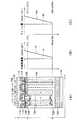
次に、本発明の実施例に係る半導体装置の構造について、図1を参照して説明する。図1は、本発明の実施例に係る半導体装置の構造を示す断面図、並びに正味の不純物濃度I(atom/cm3)及び正味のチャージ量Q(atom/cm2)と深さの関係を示すグラフである。Next, the structure of the semiconductor device according to the embodiment of the present invention will be described with reference to FIG. FIG. 1 is a cross-sectional view showing a structure of a semiconductor device according to an embodiment of the present invention, and shows a relationship between a net impurity concentration I (atom / cm3 ) and a net charge amount Q (atom / cm2 ) and a depth. It is a graph to show.
図1(A)に示すように、本発明の実施例に係る半導体装置は、n型(以下、「第1導電型」という)の不純物が埋め込まれたシリコンを用いて形成された半導体基板100と、半導体基板100上に形成された第1導電型の第1半導体領域102と、第1半導体領域102内に、半導体基板100に対して水平方向(X方向)にそれぞれ離間して形成された複数のp型(以下、「第2導電型」という)の第2半導体領域104と、第2半導体領域104に接続された第2導電型の第3半導体領域106と、第3半導体領域106上に形成された第1導電型の第4半導体領域108及び第2導電型の第5半導体領域110と、第1半導体領域102及び第3半導体領域106、並びに第4半導体領域108の一部の上に絶縁膜112を介して形成されたゲート電極114と、を備えている。また、本発明の実施例に係る半導体装置は、半導体基板100の第1半導体領域102と接していない面上に形成されたドレイン電極となる第1主電極116と、第4半導体領域108の一部及び第5半導体領域110と接続し、絶縁膜112上に形成されたソース電極となる第2主電極118と、を備えている。 As shown in FIG. 1A, a semiconductor device according to an embodiment of the present invention includes a
図1(A)に示すように、第1半導体領域102のX方向の幅Wnは、第1半導体領域102と第2半導体領域104との半導体基板100側(ドレイン電極側)の接合面(以下、「第1接合面B」という)の深さにおいてWBnであり、第1接合面Bと反対側(ソース電極側)の接合面(以下、「第2接合面T」という)の深さにおいてWTnであり、半導体基板100に対して垂直方向(Y方向)について、第1接合面Bの深さから第2接合面Tの深さに向かって一定である(WBn=WTn)。 As shown in FIG. 1A, the width Wn in the X direction of the
図1(A)に示すように、第2半導体領域104のX方向の幅Wpは、第1接合面Bの深さにおいてWBpであり、第2接合面Tの深さにおいてWTpであり、半導体基板100に対して垂直方向(Y方向)について、第1接合面Bの深さから第2接合面Tの深さに向かって一定である(WBp=WTp)。 As shown in FIG. 1A, the width Wp in the X direction of the
図1(B)に示すように、第2半導体領域104の活性化された不純物濃度と第1半導体領域102の不純物濃度との差は、第1接合面Bの深さにおいて0以上であり、半導体基板100に対して垂直方向(Y方向)について、第1接合面Bの深さから第2接合面Tの深さに向かって増加する。 As shown in FIG. 1B, the difference between the activated impurity concentration of the
その結果、図1(C)に示すように、第2半導体領域104のチャージ量Qpと第1半導体領域102のチャージ量Qnとの差ΔQが、第1接合面Bの深さにおいて0以上であり(ΔQB≧0)、半導体基板100に対して垂直方向(Y方向)について、第1接合面Bの深さから第2接合面Tの深さに向かって増加する(QBn≦QBp,QTn<QTp,ΔQB<ΔQT)。 As a result, as shown in FIG. 1C, the difference ΔQ between the charge amount Qp of the
次に、本発明の半導体装置の特性について、図2及び図3を参照して説明する。図2は、従来の半導体装置及び本発明の実施例に係る半導体装置の電界分布を示すグラフである。図3は、従来の半導体装置及び本発明の実施例に係る半導体装置の出力容量とドレイン・ソース間電圧の関係を示すグラフである。 Next, characteristics of the semiconductor device of the present invention will be described with reference to FIGS. FIG. 2 is a graph showing electric field distributions of a conventional semiconductor device and a semiconductor device according to an embodiment of the present invention. FIG. 3 is a graph showing the relationship between the output capacitance and the drain-source voltage of a conventional semiconductor device and a semiconductor device according to an embodiment of the present invention.
図2(A)は、p型及びn型の半導体領域が、それぞれ、幅及び不純物濃度が一定になるように形成されている半導体装置の電界分布を示している。図2(A)に示すように、幅及び不純物濃度が一定であるために、それらの電界分布は矩形を示す。その結果、pn構造のゲート電極に極めて近い位置にアバランシェ降伏時の電界ピーク点が現れる。 FIG. 2A shows an electric field distribution of a semiconductor device in which p-type and n-type semiconductor regions are formed so that the width and the impurity concentration are constant, respectively. As shown in FIG. 2A, since the width and the impurity concentration are constant, their electric field distributions are rectangular. As a result, an electric field peak point at the time of avalanche breakdown appears at a position very close to the gate electrode of the pn structure.
図2(B)は、特許文献3に対応する半導体装置の電界分布を示している。図2(B)に示すように、特許文献3に対応する半導体装置では、pn構造の深さ方向の中点付近にアバランシェ降伏時の電界ピーク点が現れる。 FIG. 2B shows the electric field distribution of the semiconductor device corresponding to Patent Document 3. As shown in FIG. 2B, in the semiconductor device corresponding to Patent Document 3, an electric field peak point at the time of avalanche breakdown appears near the midpoint in the depth direction of the pn structure.
図2(C)は、本発明の実施例に係る半導体装置の電界分布を示している。図2(C)に示すように、第2半導体領域104と第1半導体領域102との不純物濃度の差が、第1接合面Bの深さでは0以上であり、第1接合面Bの深さから第2接合面Tの深さに向かって増加するので、第1接合面Bの深さでは高電界となり、第2接合面Tの深さでは低電界となる。 FIG. 2C shows an electric field distribution of the semiconductor device according to the example of the present invention. As shown in FIG. 2C, the difference in impurity concentration between the
すなわち、図2(A)乃至(C)に示すように、本発明の実施例に係る半導体装置では、従来の半導体装置と比べて、第1接合面Bの深さに電界ピーク点が現れ、アバランシェポイントがゲート電極114から遠くなるので、アバランシェ耐量が改善される。また、スイッチング時のゲート電極114へのフィードバック電流が抑制されるので、スイッチング時におけるノイズが低減する。 That is, as shown in FIGS. 2A to 2C, in the semiconductor device according to the example of the present invention, an electric field peak point appears at the depth of the first bonding surface B as compared with the conventional semiconductor device, Since the avalanche point is far from the
また、図3(A)はDMOS構造の半導体装置のグラフであり、図3(B)は特許文献3に対応する半導体装置のグラフであり、図3(C)は本発明の実施例に係る半導体装置のグラフである。図3(A)乃至(C)に示すように、本発明の実施例に係る半導体装置では、従来の半導体装置と比べて、ドレイン・ソース間電圧に依存した出力容量の変化が急峻になる。その結果、スイッチング時のドリフト領域のアクセプタ及びドナーの充放電時間が短縮されるので、スイッチング時間が短縮される。特に、スイッチング時間の短縮は、半導体装置を含む回路が高周波数で動作する上で重要な特性である。この出力容量の変化が急峻になることによって内蔵されるpnダイオードの回復速度が向上する(すなわち、逆回復時間trrが短縮する)ので、内蔵されるpnダイオードの逆回復特性も改善する。 3A is a graph of a semiconductor device having a DMOS structure, FIG. 3B is a graph of a semiconductor device corresponding to Patent Document 3, and FIG. 3C is an embodiment of the present invention. It is a graph of a semiconductor device. As shown in FIGS. 3A to 3C, in the semiconductor device according to the embodiment of the present invention, the change in the output capacitance depending on the drain-source voltage becomes sharper than that in the conventional semiconductor device. As a result, the charge / discharge time of the acceptor and donor in the drift region at the time of switching is shortened, so that the switching time is shortened. In particular, shortening of the switching time is an important characteristic when a circuit including a semiconductor device operates at a high frequency. As the change in the output capacitance becomes steep, the recovery speed of the built-in pn diode is improved (that is, the reverse recovery time trr is shortened), so that the reverse recovery characteristic of the built-in pn diode is also improved.
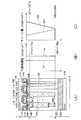
次に、本発明の実施例の変形例1について、図4を参照して説明する。図4は、本発明の実施例の変形例1に係る半導体装置の構造を示す断面図、並びに正味の活性化された不純物濃度I(atom/cm3)及び正味のチャージ量Q(atom/cm2)と深さの関係を示すグラフである。Next, a first modification of the embodiment of the present invention will be described with reference to FIG. FIG. 4 is a cross-sectional view showing the structure of the semiconductor device according to the first modification of the embodiment of the present invention, as well as the net activated impurity concentration I (atom / cm3 ) and the net charge amount Q (atom / cm). It is a graph which shows the relationship between2 ) and depth.
図4(A)に示すように、第1半導体領域102のX方向の幅Wnは、第1半導体領域102と第2半導体領域104との半導体基板100側(ドレイン電極側)の第1接合面Bの深さにおいてWBnであり、第1接合面Bと反対側(ソース電極側)の第2接合面Tの深さにおいてWTnであり、半導体基板100に対して垂直方向(Y方向)について、第1接合面Bの深さから第2接合面Tの深さに向かって減少する(WBn>WTn)。 As shown in FIG. 4A, the width Wn in the X direction of the
図4(A)に示すように、第2半導体領域104のX方向の幅Wpは、第1接合面Bの深さにおいてWBpであり、第2接合面Tの深さにおいてWTpであり、半導体基板100に対して垂直方向(Y方向)について、第1接合面Bの深さから第2接合面Tの深さに向かって増加する(WBp<WTp)。 As shown in FIG. 4A, the width Wp in the X direction of the
図4(B)に示すように、第2半導体領域104の不純物濃度Ipと第1半導体領域の不純物濃度Inとの差ΔIは、半導体基板100に対して垂直方向(Y方向)について、第1接合面Bの深さから第2接合面Tの深さに向かって常に0より大きく且つ一定である(0<ΔIB=ΔIT)。 As shown in FIG. 4B, the difference ΔI between the impurity concentration Ip of the
その結果、図4(C)に示すように、第2半導体領域104のチャージ量Qpと第1半導体領域102のチャージ量Qnとの差ΔQが、第1接合面Bの深さにおいて0以上であり(ΔQB≧0)、半導体基板100に対して垂直方向(Y方向)について、第1接合面Bの深さから第2接合面Tの深さに向かって増加する(QBn≦QBp,QTn<QTp,ΔQB<ΔQT)。 As a result, as shown in FIG. 4C, the difference ΔQ between the charge amount Qp of the
例えば、本発明の実施例の変形例1に係る半導体装置の製造方法は、以下の通りである。フォトリソグラフィー技術を用いて、反応性イオンエッチング(以下、「RIE」という)を選択的に行うことによって第1半導体領域102にトレンチを形成する。このとき、トレンチに、半導体基板100に対して垂直方向(Y方向)について、第2接合面Tの深さから第1接合面Bの深さに向かって第2半導体領域104の幅が狭くなるような角度をつける。その後、第1半導体領域104をエピタキシャル成長させる。その後、上部のMOSFET領域を形成する。 For example, the manufacturing method of the semiconductor device according to the first modification of the embodiment of the present invention is as follows. A trench is formed in the
次に、本発明の実施例の変形例2について、図5を参照して説明する。図5は、本発明の実施例の変形例2に係る半導体装置の構造を示す断面図、並びに正味の不純物濃度I(atom/cm3)及び正味のチャージ量Q(atom/cm2)と深さの関係を示すグラフである。Next, a second modification of the embodiment of the present invention will be described with reference to FIG. FIG. 5 is a cross-sectional view showing the structure of a semiconductor device according to the second modification of the embodiment of the present invention, and the net impurity concentration I (atom / cm3 ), the net charge amount Q (atom / cm2 ), and the depth. It is a graph which shows the relationship.
図5(A)に示すように、第1及び第2半導体領域102,104は、それぞれ、同様の形状を有する複数の単位層(レイヤL1乃至L6)から構成される積層構造を有している。半導体基板100に対して水平方向における第2半導体領域104の中心部(図5(A)中の実線(1))の活性化された不純物濃度は、半導体基板100に対して垂直方向について濃淡を有する波型の分布を示す。各単位層(レイヤL1乃至L6)は、活性化された不純物濃度が高い高濃度部分と、この高濃度部分を挟む活性化された不純物濃度が低い低濃度部分と、を含む層である。すなわち、第2半導体領域102の各単位層(レイヤL1乃至L6)では、1つの高濃度部分が2つの低濃度部分に挟まれている。この積層構造は、各単位層(レイヤL1乃至L6)が半導体基板100に対して垂直方向(Y方向)について繰り返し形成された構造である。 As shown in FIG. 5A, each of the first and
図5(A)に示すように、各単位層(レイヤL1乃至L6)では、第1半導体領域102のX方向の幅Wnは、境界biと境界bi+1との中間の深さにおいて最小であり、半導体基板100側(ドレイン電極側)の第1接合面Bを含む単位層(以下、「第1単位層」という)(レイヤL1)を除いて境界bi及び境界bi+1の深さにおいて最大である。例えば、単位層(レイヤL2)の第1半導体領域102のX方向の幅Wnは、境界b1と境界b2との中間の深さにおいて最小となり、境界b1及び境界b2の深さにおいて最大となる。As shown in FIG. 5A, in each unit layer (layers L1 to L6), the width Wn in the X direction of the
図5(A)に示すように、各単位層(レイヤL1乃至L6)では、第2半導体領域104のX方向の幅Wpは、境界biと境界bi+1との中間の深さにおいて最大であり、第1単位層(レイヤL1)を除いて境界bi及び境界bi+1の深さにおいて最小である。例えば、単位層(レイヤL2)の第2半導体領域104のX方向の幅Wpは、境界b1と境界b2との中間の深さにおいて最大となり、境界b1及び境界b2の深さにおいて最小となる。As shown in FIG. 5A, in each unit layer (layers L1 to L6), the width Wp in the X direction of the
また、境界biにおける第2半導体領域104の活性化された不純物濃度は、境界biと境界bi+1の中間部よりも低濃度である。このように、第1及び第2半導体領域102,104は、半導体基板100に対して垂直方向について、第2半導体領域104の高濃度部分を挟む低濃度部分の境界間の厚さで複数の単位層(レイヤL1乃至L6)に分割される。Further, the activated impurity concentration of the
また、図5(B)に示すように、各単位層(レイヤL1乃至L6)では、第2半導体領域104の不純物濃度と第1半導体領域102の不純物濃度との差は、半導体基板100側(ドレイン電極側)の境界biの深さにおいて0以上であり、境界biと境界bi+1との中間の深さにおいて最大である。Further, as shown in FIG. 5B, in each unit layer (layers L1 to L6), the difference between the impurity concentration of the
その結果、図5(C)に示すように、各単位層(レイヤL1乃至L6)のチャージ量に関して、第2半導体領域104のチャージ量Qpと第1半導体領域102のチャージ量Qnとの差ΔQが、第1単位層(レイヤL1)において0以上であり(ΔQB≧0)、半導体基板100に対して垂直方向(Y方向)の各単位層(レイヤL1乃至L6)について、第1単位層から第1接合面Bと反対側(ソース電極側)の第2接合面Tを含む単位層(以下、「第2単位層」という)(レイヤL6)に向かって増加する(ΔQB<ΔQT)。 As a result, as shown in FIG. 5C, the difference ΔQ between the charge amount Qp of the
例えば、本発明の実施例の変形例2に係る半導体装置の製造方法は、以下の通りである。半導体基板100上にn型の半導体層を形成する。その後、選択的に、n型の不純物及びp型の不純物を注入する工程と、その上にn−型領域をエピタキシャル成長させる工程と、を複数回繰り返す。このとき、各単位層(レイヤL1乃至L6)のn型拡散層及びp型拡散層を形成するときに、任意の不純物濃度を選択する。なお、n型の不純物を注入する工程を省略して、n型のエピタキシャル層にp型の不純物を注入する工程と、その上にn型領域をエピタキシャル成長させる工程と、を複数回繰り返しても良い。 For example, a method of manufacturing a semiconductor device according to the second modification of the embodiment of the present invention is as follows. An n-type semiconductor layer is formed on the
なお、本発明の実施例では、半導体基板100に対して垂直方向(Y方向)について、第1接合面Bの深さから第2接合面Tの深さに向かって第1及び第2半導体領域102,104のチャージ量Qn,Qpが線形特性を有する例について説明したが、図6に示すように、第1及び第2半導体領域102,104のチャージ量Qn,Qpの少なくとも一方が非線形特性を有していても良い。 In the embodiment of the present invention, the first and second semiconductor regions in the direction perpendicular to the semiconductor substrate 100 (Y direction) from the depth of the first bonding surface B to the depth of the second bonding surface T. Although the example in which the charge amounts Qn and Qp of 102 and 104 have linear characteristics has been described, as shown in FIG. 6, at least one of the charge amounts Qn and Qp of the first and
また、本発明の実施例では、第1半導体領域102と第2半導体領域104の繰り返しピッチ(各第2半導体領域104の離間距離)を一定としているため、全ての場合において、WBp+WBn=WTp+WTnである。 In the embodiment of the present invention, since the repetition pitch of the
また、本発明の実施例では、半導体装置の断面について説明したが、奥行き方向については、pn構造のプロファイルが延在(ストライプ)しても良いし、n型層に対して、p型領域がドット状に点在しても良い。 In the embodiment of the present invention, the cross section of the semiconductor device has been described. However, in the depth direction, the profile of the pn structure may extend (strip), and the p-type region may be formed with respect to the n-type layer. It may be dotted with dots.
また、本発明の実施例では、半導体基板100がシリコンを用いて形成されている例について説明したが、これに限られるものではなく、SiC,GaNなどを用いて形成されても良い。 In the embodiments of the present invention, the example in which the
また、本発明の実施例では、ソース・ドレイン構造を有する縦型の半導体装置について説明したが、これに限られるものではなく、例えば、10V〜1000V以上といった様々な耐圧系の半導体装置に応用することができる。 In the embodiments of the present invention, the vertical semiconductor device having the source / drain structure has been described. However, the present invention is not limited to this, and the present invention is applied to various withstand voltage semiconductor devices such as 10 V to 1000 V or more. be able to.
本発明の実施例によれば、第1接合面Bの深さに電界ピーク点が現れ、アバランシェポイントがゲート電極114から遠くなるので、アバランシェ耐量を向上させることができ、且つ、素子の信頼性を向上させることができる。 According to the embodiment of the present invention, the electric field peak point appears at the depth of the first junction surface B, and the avalanche point is far from the
また、本発明の実施例によれば、スイッチング時のゲート電極114へのフィードバック電流が抑制されるので、スイッチング時におけるノイズを低減することができる。 Further, according to the embodiment of the present invention, the feedback current to the
また、本発明の実施例によれば、第2半導体領域104のチャージ量Qpと第1半導体領域102のチャージ量Qnとの差ΔQが第1接合面Bの深さにおいて0以上となり、ドリフト領域の深い部分の電界のみが高くなるので、アバランシェ耐量をさらに向上させることができる。 Further, according to the embodiment of the present invention, the difference ΔQ between the charge amount Qp of the
また、本発明の実施例によれば、第2半導体領域104のチャージ量Qpと第1半導体領域102のチャージ量Qnとの差ΔQが第1接合面Bの深さにおいて0である場合には、半導体装置のオン抵抗を低減することができる。 Further, according to the embodiment of the present invention, when the difference ΔQ between the charge amount Qp of the
100 半導体基板
102 第1半導体領域
104 第2半導体領域
106 第3半導体領域
108 第4半導体領域
110 第5半導体領域
112 絶縁膜
114 ゲート電極
116 第1主電極
118 第2主電極
B 第1接合面
T 第2接合面100
Claims (4)
Translated fromJapanese前記半導体基板上に形成された第1導電型の第1半導体領域と、
前記第1半導体領域内に、前記半導体基板に対して水平方向にそれぞれ離間して形成さ
れ、前記水平方向において前記第1半導体領域の一部と交互に並び、前記半導体基板に対
して垂直方向において前記半導体基板側に延び、前記半導体基板側において前記第1半導
体領域との界面をなす複数の第2導電型の第2半導体領域と、
前記第2半導体領域に接続され、前記第1半導体領域の表面側に設けられた複数の第2
導電型の第3半導体領域と、
前記第1半導体領域の表面に絶縁膜を介して設けられたゲート電極を備え、
前記第1半導体領域と前記複数の第2半導体領域は、スーパージャンクション構造を形
成し、
前記界面は、前記ゲート電極から離れるように、前記垂直方向における前記第1半導体
領域の中心よりも前記半導体基板側に位置し、
前記第2半導体領域のチャージ量と前記第1半導体領域のチャージ量との差は、前記界
面において0以上であり、且つ前記垂直方向において、前記第3半導体領域に向って増加
することを特徴とする半導体装置。A first conductivity type semiconductor substrate;
A first conductivity type first semiconductor region formed on the semiconductor substrate;
Said first semiconductor region, wherein the spaced apart respectively in the horizontal direction with respect to the semiconductor substrate, parallelBeauty alternately with a portion of said first semiconductor region in the horizontaldirection, against the said semiconductor substrate
Extending in the vertical direction to the semiconductor substrate side, and the first semiconductor on the semiconductor substrate side.
A plurality of second conductivity type second semiconductor regionsforming an interface with the body region ;
A plurality of second layers connected to the second semiconductor regionand provided on the surface side of the first semiconductor region .
A third semiconductor region of conductivity type;
A gate electrode provided on the surface of the first semiconductor region via an insulating film ;
The first semiconductor region and the plurality of second semiconductor regions form a super junction structure.
And
The first semiconductor in the vertical direction is separated from the gate electrode.
Located closer to the semiconductor substrate than the center of the region,
The difference between the charge amount of the second semiconductor region and the charge amount of the first semiconductor region is not less than 0 at the interface, and increasestoward the third semiconductor region in the vertical direction. Semiconductor device.
前記第2半導体領域の不純物濃度は、前記半導体基板から前記垂直方向に離れるに従っ
て増加する請求項1に記載の半導体装置。The horizontal width of the second semiconductor region is constant in the vertical direction,
2. The semiconductor device according to claim 1, wherein the impurity concentration of the second semiconductor region increases with increasing distance from the semiconductor substrate in the vertical direction.
に従って広がり、
前記第2半導体領域の不純物濃度は、前記垂直方向において一定である請求項1に記載
の半導体装置。The horizontal width of the second semiconductor region increases with distance from the semiconductor substrate in the vertical direction,
The semiconductor device according to claim 1, wherein an impurity concentration of the second semiconductor region is constant in the vertical direction.
1に記載の半導体装置。2. The semiconductor device according to claim 1, wherein the impurity concentration of the second semiconductor region has a waveform distribution in the vertical direction.
Priority Applications (3)
| Application Number | Priority Date | Filing Date | Title |
|---|---|---|---|
| JP2009012610AJP5484741B2 (en) | 2009-01-23 | 2009-01-23 | Semiconductor device |
| CN2010100040231ACN101794816B (en) | 2009-01-23 | 2010-01-14 | Semiconductor device |
| US12/692,527US8159023B2 (en) | 2009-01-23 | 2010-01-22 | Semiconductor device |
Applications Claiming Priority (1)
| Application Number | Priority Date | Filing Date | Title |
|---|---|---|---|
| JP2009012610AJP5484741B2 (en) | 2009-01-23 | 2009-01-23 | Semiconductor device |
Publications (3)
| Publication Number | Publication Date |
|---|---|
| JP2010171221A JP2010171221A (en) | 2010-08-05 |
| JP2010171221A5 JP2010171221A5 (en) | 2013-03-28 |
| JP5484741B2true JP5484741B2 (en) | 2014-05-07 |
Family
ID=42353476
Family Applications (1)
| Application Number | Title | Priority Date | Filing Date |
|---|---|---|---|
| JP2009012610AActiveJP5484741B2 (en) | 2009-01-23 | 2009-01-23 | Semiconductor device |
Country Status (3)
| Country | Link |
|---|---|
| US (1) | US8159023B2 (en) |
| JP (1) | JP5484741B2 (en) |
| CN (1) | CN101794816B (en) |
Families Citing this family (18)
| Publication number | Priority date | Publication date | Assignee | Title |
|---|---|---|---|---|
| JP5739813B2 (en)* | 2009-09-15 | 2015-06-24 | 株式会社東芝 | Semiconductor device |
| JP2011204796A (en)* | 2010-03-24 | 2011-10-13 | Toshiba Corp | Semiconductor apparatus, and method of manufacturing the same |
| KR101216897B1 (en) | 2011-08-09 | 2012-12-28 | 주식회사 케이이씨 | High voltage semiconductor device |
| KR101279222B1 (en) | 2011-08-26 | 2013-06-26 | 주식회사 케이이씨 | High voltage semiconductor device |
| US9287371B2 (en) | 2012-10-05 | 2016-03-15 | Semiconductor Components Industries, Llc | Semiconductor device having localized charge balance structure and method |
| US9219138B2 (en) | 2012-10-05 | 2015-12-22 | Semiconductor Components Industries, Llc | Semiconductor device having localized charge balance structure and method |
| US10256325B2 (en)* | 2012-11-08 | 2019-04-09 | Infineon Technologies Austria Ag | Radiation-hardened power semiconductor devices and methods of forming them |
| CN103199104B (en)* | 2013-03-05 | 2016-04-27 | 矽力杰半导体技术(杭州)有限公司 | A kind of crystal circle structure and apply its power device |
| SE1550821A1 (en)* | 2015-06-16 | 2016-11-22 | Ascatron Ab | SiC SUPER-JUNCTIONS |
| US9768247B1 (en) | 2016-05-06 | 2017-09-19 | Semiconductor Components Industries, Llc | Semiconductor device having improved superjunction trench structure and method of manufacture |
| US20190221664A1 (en)* | 2016-09-02 | 2019-07-18 | Shindengen Electric Manufacturing Co., Ltd. | Mosfet and power conversion circuit |
| WO2018051512A1 (en)* | 2016-09-16 | 2018-03-22 | 新電元工業株式会社 | Mosfet and power conversion circuit |
| WO2018087896A1 (en)* | 2016-11-11 | 2018-05-17 | 新電元工業株式会社 | Mosfet and power conversion circuit |
| US10872952B1 (en)* | 2017-05-26 | 2020-12-22 | Shindengen Electric Manufacturing Co., Ltd. | MOSFET and power conversion circuit |
| JP2019054169A (en)* | 2017-09-15 | 2019-04-04 | 株式会社東芝 | Semiconductor device |
| JP6556948B1 (en)* | 2017-11-17 | 2019-08-07 | 新電元工業株式会社 | Power conversion circuit |
| CN110416285B (en)* | 2019-07-31 | 2024-06-07 | 电子科技大学 | A super junction power DMOS device |
| JP2023139376A (en)* | 2022-03-22 | 2023-10-04 | 国立研究開発法人産業技術総合研究所 | silicon carbide semiconductor device |
Family Cites Families (13)
| Publication number | Priority date | Publication date | Assignee | Title |
|---|---|---|---|---|
| DE69833743T2 (en)* | 1998-12-09 | 2006-11-09 | Stmicroelectronics S.R.L., Agrate Brianza | Manufacturing method of an integrated edge structure for high voltage semiconductor devices |
| DE69838453D1 (en)* | 1998-12-09 | 2007-10-31 | St Microelectronics Srl | Power component with MOS-gate for high voltages and related manufacturing process |
| JP3743395B2 (en) | 2002-06-03 | 2006-02-08 | 株式会社デンソー | Semiconductor device manufacturing method and semiconductor device |
| JP4304433B2 (en)* | 2002-06-14 | 2009-07-29 | 富士電機デバイステクノロジー株式会社 | Semiconductor element |
| JP3634830B2 (en)* | 2002-09-25 | 2005-03-30 | 株式会社東芝 | Power semiconductor device |
| JP4904673B2 (en)* | 2004-02-09 | 2012-03-28 | 富士電機株式会社 | Semiconductor device and manufacturing method of semiconductor device |
| JP4851738B2 (en) | 2005-06-29 | 2012-01-11 | 新電元工業株式会社 | Semiconductor device |
| WO2007122646A1 (en) | 2006-04-21 | 2007-11-01 | Stmicroelectronics S.R.L. | Process for manufacturing a power semiconductor device and corresponding power semiconductor device |
| EP1873837B1 (en)* | 2006-06-28 | 2013-03-27 | STMicroelectronics Srl | Semiconductor power device having an edge-termination structure and manufacturing method thereof |
| JP2008153620A (en)* | 2006-11-21 | 2008-07-03 | Toshiba Corp | Semiconductor device |
| JP2008210899A (en)* | 2007-02-23 | 2008-09-11 | Toshiba Corp | Semiconductor device and manufacturing method thereof |
| JP4564509B2 (en)* | 2007-04-05 | 2010-10-20 | 株式会社東芝 | Power semiconductor device |
| JP2008294028A (en)* | 2007-05-22 | 2008-12-04 | Toshiba Corp | Semiconductor device |
- 2009
- 2009-01-23JPJP2009012610Apatent/JP5484741B2/enactiveActive
- 2010
- 2010-01-14CNCN2010100040231Apatent/CN101794816B/enactiveActive
- 2010-01-22USUS12/692,527patent/US8159023B2/enactiveActive
Also Published As
| Publication number | Publication date |
|---|---|
| US8159023B2 (en) | 2012-04-17 |
| CN101794816B (en) | 2012-10-10 |
| US20100187604A1 (en) | 2010-07-29 |
| CN101794816A (en) | 2010-08-04 |
| JP2010171221A (en) | 2010-08-05 |
Similar Documents
| Publication | Publication Date | Title |
|---|---|---|
| JP5484741B2 (en) | Semiconductor device | |
| JP5762689B2 (en) | Semiconductor device | |
| CN102403315B (en) | Semiconductor device | |
| JP3634830B2 (en) | Power semiconductor device | |
| JP5504235B2 (en) | Semiconductor device | |
| JP5002148B2 (en) | Semiconductor device | |
| JP5198030B2 (en) | Semiconductor element | |
| JP4832731B2 (en) | Power semiconductor device | |
| US9590030B2 (en) | Semiconductor device having diode characteristic | |
| US20080035992A1 (en) | Semiconductor device | |
| JP2009088345A (en) | Semiconductor device | |
| US8592917B2 (en) | Semiconductor device and method for manufacturing same | |
| CN101478000A (en) | Improved sawtooth electric field drift region structure for power semiconductor devices | |
| JP2009272397A (en) | Semiconductor device | |
| JP2009188177A (en) | Semiconductor device and manufacturing method thereof | |
| JP5201307B2 (en) | Semiconductor device | |
| US8581298B2 (en) | Semiconductor device | |
| JP6560141B2 (en) | Switching element | |
| TW201803125A (en) | Vertical niobium metal oxide semiconductor field effect transistor | |
| JP2009105219A (en) | Semiconductor device | |
| CN111697056A (en) | Semiconductor device and method for manufacturing the same | |
| CN102412298B (en) | Semiconductor Element And Manufacturing Method Thereof | |
| JP5448733B2 (en) | Manufacturing method of semiconductor device | |
| KR20130017054A (en) | Semiconductor device and method for manufacturing the same | |
| JP6089070B2 (en) | Semiconductor device |
Legal Events
| Date | Code | Title | Description |
|---|---|---|---|
| A621 | Written request for application examination | Free format text:JAPANESE INTERMEDIATE CODE: A621 Effective date:20110228 | |
| A521 | Request for written amendment filed | Free format text:JAPANESE INTERMEDIATE CODE: A523 Effective date:20130207 | |
| A871 | Explanation of circumstances concerning accelerated examination | Free format text:JAPANESE INTERMEDIATE CODE: A871 Effective date:20130207 | |
| A977 | Report on retrieval | Free format text:JAPANESE INTERMEDIATE CODE: A971007 Effective date:20130218 | |
| A975 | Report on accelerated examination | Free format text:JAPANESE INTERMEDIATE CODE: A971005 Effective date:20130219 | |
| A131 | Notification of reasons for refusal | Free format text:JAPANESE INTERMEDIATE CODE: A131 Effective date:20130222 | |
| A521 | Request for written amendment filed | Free format text:JAPANESE INTERMEDIATE CODE: A523 Effective date:20130412 | |
| A131 | Notification of reasons for refusal | Free format text:JAPANESE INTERMEDIATE CODE: A131 Effective date:20130712 | |
| A521 | Request for written amendment filed | Free format text:JAPANESE INTERMEDIATE CODE: A523 Effective date:20130910 | |
| A02 | Decision of refusal | Free format text:JAPANESE INTERMEDIATE CODE: A02 Effective date:20131001 | |
| A521 | Request for written amendment filed | Free format text:JAPANESE INTERMEDIATE CODE: A523 Effective date:20131219 | |
| A911 | Transfer to examiner for re-examination before appeal (zenchi) | Free format text:JAPANESE INTERMEDIATE CODE: A911 Effective date:20131226 | |
| TRDD | Decision of grant or rejection written | ||
| A01 | Written decision to grant a patent or to grant a registration (utility model) | Free format text:JAPANESE INTERMEDIATE CODE: A01 Effective date:20140124 | |
| A61 | First payment of annual fees (during grant procedure) | Free format text:JAPANESE INTERMEDIATE CODE: A61 Effective date:20140219 | |
| R151 | Written notification of patent or utility model registration | Ref document number:5484741 Country of ref document:JP Free format text:JAPANESE INTERMEDIATE CODE: R151 |