JP5482196B2 - Film forming apparatus, film forming method, and storage medium - Google Patents
Film forming apparatus, film forming method, and storage mediumDownload PDFInfo
- Publication number
- JP5482196B2 JP5482196B2JP2009295351AJP2009295351AJP5482196B2JP 5482196 B2JP5482196 B2JP 5482196B2JP 2009295351 AJP2009295351 AJP 2009295351AJP 2009295351 AJP2009295351 AJP 2009295351AJP 5482196 B2JP5482196 B2JP 5482196B2
- Authority
- JP
- Japan
- Prior art keywords
- gas
- reaction gas
- separation
- substrate
- gas supply
- Prior art date
- Legal status (The legal status is an assumption and is not a legal conclusion. Google has not performed a legal analysis and makes no representation as to the accuracy of the status listed.)
- Active
Links
- 238000000034methodMethods0.000titleclaimsdescription39
- 238000003860storageMethods0.000titleclaimsdescription6
- 239000007789gasSubstances0.000claimsdescription205
- 239000012495reaction gasSubstances0.000claimsdescription116
- 238000000926separation methodMethods0.000claimsdescription89
- 238000012545processingMethods0.000claimsdescription84
- 239000000758substrateSubstances0.000claimsdescription47
- NRTOMJZYCJJWKI-UHFFFAOYSA-NTitanium nitrideChemical compound[Ti]#NNRTOMJZYCJJWKI-UHFFFAOYSA-N0.000claimsdescription17
- 230000015572biosynthetic processEffects0.000claimsdescription13
- 238000006243chemical reactionMethods0.000claimsdescription11
- 239000010936titaniumSubstances0.000claimsdescription11
- 230000007246mechanismEffects0.000claimsdescription9
- 239000004020conductorSubstances0.000claimsdescription8
- 238000002156mixingMethods0.000claimsdescription7
- 239000000203mixtureSubstances0.000claimsdescription5
- 239000010408filmSubstances0.000description145
- ATJFFYVFTNAWJD-UHFFFAOYSA-NTinChemical compound[Sn]ATJFFYVFTNAWJD-UHFFFAOYSA-N0.000description65
- 235000012431wafersNutrition0.000description61
- QGZKDVFQNNGYKY-UHFFFAOYSA-NAmmoniaChemical compoundNQGZKDVFQNNGYKY-UHFFFAOYSA-N0.000description42
- 238000001179sorption measurementMethods0.000description29
- 239000010410layerSubstances0.000description24
- XJDNKRIXUMDJCW-UHFFFAOYSA-Jtitanium tetrachlorideChemical compoundCl[Ti](Cl)(Cl)ClXJDNKRIXUMDJCW-UHFFFAOYSA-J0.000description21
- 229910003074TiCl4Inorganic materials0.000description20
- 229910000069nitrogen hydrideInorganic materials0.000description19
- 230000002093peripheral effectEffects0.000description19
- 239000010409thin filmSubstances0.000description18
- 238000002425crystallisationMethods0.000description16
- 230000008025crystallizationEffects0.000description16
- 230000008569processEffects0.000description13
- 239000007795chemical reaction productSubstances0.000description11
- 239000002245particleSubstances0.000description9
- 238000010926purgeMethods0.000description9
- 238000012546transferMethods0.000description9
- 238000000231atomic layer depositionMethods0.000description8
- 238000011144upstream manufacturingMethods0.000description8
- 230000005012migrationEffects0.000description7
- 238000013508migrationMethods0.000description7
- 229920006395saturated elastomerPolymers0.000description7
- 238000005229chemical vapour depositionMethods0.000description6
- 230000000694effectsEffects0.000description6
- 239000012535impuritySubstances0.000description6
- IJGRMHOSHXDMSA-UHFFFAOYSA-NAtomic nitrogenChemical compoundN#NIJGRMHOSHXDMSA-UHFFFAOYSA-N0.000description5
- 230000004888barrier functionEffects0.000description5
- GWEVSGVZZGPLCZ-UHFFFAOYSA-NTitan oxideChemical compoundO=[Ti]=OGWEVSGVZZGPLCZ-UHFFFAOYSA-N0.000description4
- 230000009471actionEffects0.000description4
- 239000000460chlorineSubstances0.000description4
- 238000010586diagramMethods0.000description4
- 238000002474experimental methodMethods0.000description4
- 238000010438heat treatmentMethods0.000description4
- 239000011229interlayerSubstances0.000description4
- BPUBBGLMJRNUCC-UHFFFAOYSA-Noxygen(2-);tantalum(5+)Chemical compound[O-2].[O-2].[O-2].[O-2].[O-2].[Ta+5].[Ta+5]BPUBBGLMJRNUCC-UHFFFAOYSA-N0.000description4
- RVTZCBVAJQQJTK-UHFFFAOYSA-Noxygen(2-);zirconium(4+)Chemical compound[O-2].[O-2].[Zr+4]RVTZCBVAJQQJTK-UHFFFAOYSA-N0.000description4
- 238000002407reformingMethods0.000description4
- 239000004065semiconductorSubstances0.000description4
- 229910001936tantalum oxideInorganic materials0.000description4
- OGIDPMRJRNCKJF-UHFFFAOYSA-Ntitanium oxideInorganic materials[Ti]=OOGIDPMRJRNCKJF-UHFFFAOYSA-N0.000description4
- 229910001928zirconium oxideInorganic materials0.000description4
- KZBUYRJDOAKODT-UHFFFAOYSA-NChlorineChemical compoundClClKZBUYRJDOAKODT-UHFFFAOYSA-N0.000description3
- 229910052782aluminiumInorganic materials0.000description3
- XAGFODPZIPBFFR-UHFFFAOYSA-NaluminiumChemical compound[Al]XAGFODPZIPBFFR-UHFFFAOYSA-N0.000description3
- 239000003990capacitorSubstances0.000description3
- 238000005121nitridingMethods0.000description3
- 230000001105regulatory effectEffects0.000description3
- XKRFYHLGVUSROY-UHFFFAOYSA-NArgonChemical compound[Ar]XKRFYHLGVUSROY-UHFFFAOYSA-N0.000description2
- RTAQQCXQSZGOHL-UHFFFAOYSA-NTitaniumChemical compound[Ti]RTAQQCXQSZGOHL-UHFFFAOYSA-N0.000description2
- 229910021529ammoniaInorganic materials0.000description2
- 229910052801chlorineInorganic materials0.000description2
- 230000000052comparative effectEffects0.000description2
- 238000000151depositionMethods0.000description2
- 230000008021depositionEffects0.000description2
- 230000006866deteriorationEffects0.000description2
- 238000007599dischargingMethods0.000description2
- 239000011261inert gasSubstances0.000description2
- 238000002955isolationMethods0.000description2
- 239000012528membraneSubstances0.000description2
- 229910052751metalInorganic materials0.000description2
- 239000002184metalSubstances0.000description2
- 229910052757nitrogenInorganic materials0.000description2
- 238000009832plasma treatmentMethods0.000description2
- 230000003746surface roughnessEffects0.000description2
- 229910052719titaniumInorganic materials0.000description2
- 229910052786argonInorganic materials0.000description1
- 230000001276controlling effectEffects0.000description1
- 238000000354decomposition reactionMethods0.000description1
- 230000000994depressogenic effectEffects0.000description1
- 238000009792diffusion processMethods0.000description1
- 230000006870functionEffects0.000description1
- 150000002500ionsChemical class0.000description1
- 238000005259measurementMethods0.000description1
- 239000007769metal materialSubstances0.000description1
- 239000002052molecular layerSubstances0.000description1
- 238000005192partitionMethods0.000description1
- 230000001681protective effectEffects0.000description1
- 239000010453quartzSubstances0.000description1
- 230000009467reductionEffects0.000description1
- 230000000630rising effectEffects0.000description1
- VYPSYNLAJGMNEJ-UHFFFAOYSA-Nsilicon dioxideInorganic materialsO=[Si]=OVYPSYNLAJGMNEJ-UHFFFAOYSA-N0.000description1
Images


Classifications
- C—CHEMISTRY; METALLURGY
- C23—COATING METALLIC MATERIAL; COATING MATERIAL WITH METALLIC MATERIAL; CHEMICAL SURFACE TREATMENT; DIFFUSION TREATMENT OF METALLIC MATERIAL; COATING BY VACUUM EVAPORATION, BY SPUTTERING, BY ION IMPLANTATION OR BY CHEMICAL VAPOUR DEPOSITION, IN GENERAL; INHIBITING CORROSION OF METALLIC MATERIAL OR INCRUSTATION IN GENERAL
- C23C—COATING METALLIC MATERIAL; COATING MATERIAL WITH METALLIC MATERIAL; SURFACE TREATMENT OF METALLIC MATERIAL BY DIFFUSION INTO THE SURFACE, BY CHEMICAL CONVERSION OR SUBSTITUTION; COATING BY VACUUM EVAPORATION, BY SPUTTERING, BY ION IMPLANTATION OR BY CHEMICAL VAPOUR DEPOSITION, IN GENERAL
- C23C16/00—Chemical coating by decomposition of gaseous compounds, without leaving reaction products of surface material in the coating, i.e. chemical vapour deposition [CVD] processes
- C23C16/44—Chemical coating by decomposition of gaseous compounds, without leaving reaction products of surface material in the coating, i.e. chemical vapour deposition [CVD] processes characterised by the method of coating
- C23C16/458—Chemical coating by decomposition of gaseous compounds, without leaving reaction products of surface material in the coating, i.e. chemical vapour deposition [CVD] processes characterised by the method of coating characterised by the method used for supporting substrates in the reaction chamber
- C23C16/4582—Rigid and flat substrates, e.g. plates or discs
- C23C16/4583—Rigid and flat substrates, e.g. plates or discs the substrate being supported substantially horizontally
- C23C16/4584—Rigid and flat substrates, e.g. plates or discs the substrate being supported substantially horizontally the substrate being rotated
- C—CHEMISTRY; METALLURGY
- C23—COATING METALLIC MATERIAL; COATING MATERIAL WITH METALLIC MATERIAL; CHEMICAL SURFACE TREATMENT; DIFFUSION TREATMENT OF METALLIC MATERIAL; COATING BY VACUUM EVAPORATION, BY SPUTTERING, BY ION IMPLANTATION OR BY CHEMICAL VAPOUR DEPOSITION, IN GENERAL; INHIBITING CORROSION OF METALLIC MATERIAL OR INCRUSTATION IN GENERAL
- C23C—COATING METALLIC MATERIAL; COATING MATERIAL WITH METALLIC MATERIAL; SURFACE TREATMENT OF METALLIC MATERIAL BY DIFFUSION INTO THE SURFACE, BY CHEMICAL CONVERSION OR SUBSTITUTION; COATING BY VACUUM EVAPORATION, BY SPUTTERING, BY ION IMPLANTATION OR BY CHEMICAL VAPOUR DEPOSITION, IN GENERAL
- C23C16/00—Chemical coating by decomposition of gaseous compounds, without leaving reaction products of surface material in the coating, i.e. chemical vapour deposition [CVD] processes
- C23C16/22—Chemical coating by decomposition of gaseous compounds, without leaving reaction products of surface material in the coating, i.e. chemical vapour deposition [CVD] processes characterised by the deposition of inorganic material, other than metallic material
- C23C16/30—Deposition of compounds, mixtures or solid solutions, e.g. borides, carbides, nitrides
- C23C16/34—Nitrides
- C—CHEMISTRY; METALLURGY
- C23—COATING METALLIC MATERIAL; COATING MATERIAL WITH METALLIC MATERIAL; CHEMICAL SURFACE TREATMENT; DIFFUSION TREATMENT OF METALLIC MATERIAL; COATING BY VACUUM EVAPORATION, BY SPUTTERING, BY ION IMPLANTATION OR BY CHEMICAL VAPOUR DEPOSITION, IN GENERAL; INHIBITING CORROSION OF METALLIC MATERIAL OR INCRUSTATION IN GENERAL
- C23C—COATING METALLIC MATERIAL; COATING MATERIAL WITH METALLIC MATERIAL; SURFACE TREATMENT OF METALLIC MATERIAL BY DIFFUSION INTO THE SURFACE, BY CHEMICAL CONVERSION OR SUBSTITUTION; COATING BY VACUUM EVAPORATION, BY SPUTTERING, BY ION IMPLANTATION OR BY CHEMICAL VAPOUR DEPOSITION, IN GENERAL
- C23C16/00—Chemical coating by decomposition of gaseous compounds, without leaving reaction products of surface material in the coating, i.e. chemical vapour deposition [CVD] processes
- C23C16/44—Chemical coating by decomposition of gaseous compounds, without leaving reaction products of surface material in the coating, i.e. chemical vapour deposition [CVD] processes characterised by the method of coating
- C23C16/4412—Details relating to the exhausts, e.g. pumps, filters, scrubbers, particle traps
- C—CHEMISTRY; METALLURGY
- C23—COATING METALLIC MATERIAL; COATING MATERIAL WITH METALLIC MATERIAL; CHEMICAL SURFACE TREATMENT; DIFFUSION TREATMENT OF METALLIC MATERIAL; COATING BY VACUUM EVAPORATION, BY SPUTTERING, BY ION IMPLANTATION OR BY CHEMICAL VAPOUR DEPOSITION, IN GENERAL; INHIBITING CORROSION OF METALLIC MATERIAL OR INCRUSTATION IN GENERAL
- C23C—COATING METALLIC MATERIAL; COATING MATERIAL WITH METALLIC MATERIAL; SURFACE TREATMENT OF METALLIC MATERIAL BY DIFFUSION INTO THE SURFACE, BY CHEMICAL CONVERSION OR SUBSTITUTION; COATING BY VACUUM EVAPORATION, BY SPUTTERING, BY ION IMPLANTATION OR BY CHEMICAL VAPOUR DEPOSITION, IN GENERAL
- C23C16/00—Chemical coating by decomposition of gaseous compounds, without leaving reaction products of surface material in the coating, i.e. chemical vapour deposition [CVD] processes
- C23C16/44—Chemical coating by decomposition of gaseous compounds, without leaving reaction products of surface material in the coating, i.e. chemical vapour deposition [CVD] processes characterised by the method of coating
- C23C16/455—Chemical coating by decomposition of gaseous compounds, without leaving reaction products of surface material in the coating, i.e. chemical vapour deposition [CVD] processes characterised by the method of coating characterised by the method used for introducing gases into reaction chamber or for modifying gas flows in reaction chamber
- C23C16/45519—Inert gas curtains
- C—CHEMISTRY; METALLURGY
- C23—COATING METALLIC MATERIAL; COATING MATERIAL WITH METALLIC MATERIAL; CHEMICAL SURFACE TREATMENT; DIFFUSION TREATMENT OF METALLIC MATERIAL; COATING BY VACUUM EVAPORATION, BY SPUTTERING, BY ION IMPLANTATION OR BY CHEMICAL VAPOUR DEPOSITION, IN GENERAL; INHIBITING CORROSION OF METALLIC MATERIAL OR INCRUSTATION IN GENERAL
- C23C—COATING METALLIC MATERIAL; COATING MATERIAL WITH METALLIC MATERIAL; SURFACE TREATMENT OF METALLIC MATERIAL BY DIFFUSION INTO THE SURFACE, BY CHEMICAL CONVERSION OR SUBSTITUTION; COATING BY VACUUM EVAPORATION, BY SPUTTERING, BY ION IMPLANTATION OR BY CHEMICAL VAPOUR DEPOSITION, IN GENERAL
- C23C16/00—Chemical coating by decomposition of gaseous compounds, without leaving reaction products of surface material in the coating, i.e. chemical vapour deposition [CVD] processes
- C23C16/44—Chemical coating by decomposition of gaseous compounds, without leaving reaction products of surface material in the coating, i.e. chemical vapour deposition [CVD] processes characterised by the method of coating
- C23C16/455—Chemical coating by decomposition of gaseous compounds, without leaving reaction products of surface material in the coating, i.e. chemical vapour deposition [CVD] processes characterised by the method of coating characterised by the method used for introducing gases into reaction chamber or for modifying gas flows in reaction chamber
- C23C16/45523—Pulsed gas flow or change of composition over time
- C—CHEMISTRY; METALLURGY
- C23—COATING METALLIC MATERIAL; COATING MATERIAL WITH METALLIC MATERIAL; CHEMICAL SURFACE TREATMENT; DIFFUSION TREATMENT OF METALLIC MATERIAL; COATING BY VACUUM EVAPORATION, BY SPUTTERING, BY ION IMPLANTATION OR BY CHEMICAL VAPOUR DEPOSITION, IN GENERAL; INHIBITING CORROSION OF METALLIC MATERIAL OR INCRUSTATION IN GENERAL
- C23C—COATING METALLIC MATERIAL; COATING MATERIAL WITH METALLIC MATERIAL; SURFACE TREATMENT OF METALLIC MATERIAL BY DIFFUSION INTO THE SURFACE, BY CHEMICAL CONVERSION OR SUBSTITUTION; COATING BY VACUUM EVAPORATION, BY SPUTTERING, BY ION IMPLANTATION OR BY CHEMICAL VAPOUR DEPOSITION, IN GENERAL
- C23C16/00—Chemical coating by decomposition of gaseous compounds, without leaving reaction products of surface material in the coating, i.e. chemical vapour deposition [CVD] processes
- C23C16/44—Chemical coating by decomposition of gaseous compounds, without leaving reaction products of surface material in the coating, i.e. chemical vapour deposition [CVD] processes characterised by the method of coating
- C23C16/455—Chemical coating by decomposition of gaseous compounds, without leaving reaction products of surface material in the coating, i.e. chemical vapour deposition [CVD] processes characterised by the method of coating characterised by the method used for introducing gases into reaction chamber or for modifying gas flows in reaction chamber
- C23C16/45587—Mechanical means for changing the gas flow
- C23C16/45591—Fixed means, e.g. wings, baffles
- C—CHEMISTRY; METALLURGY
- C23—COATING METALLIC MATERIAL; COATING MATERIAL WITH METALLIC MATERIAL; CHEMICAL SURFACE TREATMENT; DIFFUSION TREATMENT OF METALLIC MATERIAL; COATING BY VACUUM EVAPORATION, BY SPUTTERING, BY ION IMPLANTATION OR BY CHEMICAL VAPOUR DEPOSITION, IN GENERAL; INHIBITING CORROSION OF METALLIC MATERIAL OR INCRUSTATION IN GENERAL
- C23C—COATING METALLIC MATERIAL; COATING MATERIAL WITH METALLIC MATERIAL; SURFACE TREATMENT OF METALLIC MATERIAL BY DIFFUSION INTO THE SURFACE, BY CHEMICAL CONVERSION OR SUBSTITUTION; COATING BY VACUUM EVAPORATION, BY SPUTTERING, BY ION IMPLANTATION OR BY CHEMICAL VAPOUR DEPOSITION, IN GENERAL
- C23C16/00—Chemical coating by decomposition of gaseous compounds, without leaving reaction products of surface material in the coating, i.e. chemical vapour deposition [CVD] processes
- C23C16/44—Chemical coating by decomposition of gaseous compounds, without leaving reaction products of surface material in the coating, i.e. chemical vapour deposition [CVD] processes characterised by the method of coating
- C23C16/458—Chemical coating by decomposition of gaseous compounds, without leaving reaction products of surface material in the coating, i.e. chemical vapour deposition [CVD] processes characterised by the method of coating characterised by the method used for supporting substrates in the reaction chamber
- C23C16/4582—Rigid and flat substrates, e.g. plates or discs
- C23C16/4583—Rigid and flat substrates, e.g. plates or discs the substrate being supported substantially horizontally
- C23C16/4585—Devices at or outside the perimeter of the substrate support, e.g. clamping rings, shrouds
- C—CHEMISTRY; METALLURGY
- C23—COATING METALLIC MATERIAL; COATING MATERIAL WITH METALLIC MATERIAL; CHEMICAL SURFACE TREATMENT; DIFFUSION TREATMENT OF METALLIC MATERIAL; COATING BY VACUUM EVAPORATION, BY SPUTTERING, BY ION IMPLANTATION OR BY CHEMICAL VAPOUR DEPOSITION, IN GENERAL; INHIBITING CORROSION OF METALLIC MATERIAL OR INCRUSTATION IN GENERAL
- C23C—COATING METALLIC MATERIAL; COATING MATERIAL WITH METALLIC MATERIAL; SURFACE TREATMENT OF METALLIC MATERIAL BY DIFFUSION INTO THE SURFACE, BY CHEMICAL CONVERSION OR SUBSTITUTION; COATING BY VACUUM EVAPORATION, BY SPUTTERING, BY ION IMPLANTATION OR BY CHEMICAL VAPOUR DEPOSITION, IN GENERAL
- C23C16/00—Chemical coating by decomposition of gaseous compounds, without leaving reaction products of surface material in the coating, i.e. chemical vapour deposition [CVD] processes
- C23C16/44—Chemical coating by decomposition of gaseous compounds, without leaving reaction products of surface material in the coating, i.e. chemical vapour deposition [CVD] processes characterised by the method of coating
- C23C16/50—Chemical coating by decomposition of gaseous compounds, without leaving reaction products of surface material in the coating, i.e. chemical vapour deposition [CVD] processes characterised by the method of coating using electric discharges
- C—CHEMISTRY; METALLURGY
- C23—COATING METALLIC MATERIAL; COATING MATERIAL WITH METALLIC MATERIAL; CHEMICAL SURFACE TREATMENT; DIFFUSION TREATMENT OF METALLIC MATERIAL; COATING BY VACUUM EVAPORATION, BY SPUTTERING, BY ION IMPLANTATION OR BY CHEMICAL VAPOUR DEPOSITION, IN GENERAL; INHIBITING CORROSION OF METALLIC MATERIAL OR INCRUSTATION IN GENERAL
- C23C—COATING METALLIC MATERIAL; COATING MATERIAL WITH METALLIC MATERIAL; SURFACE TREATMENT OF METALLIC MATERIAL BY DIFFUSION INTO THE SURFACE, BY CHEMICAL CONVERSION OR SUBSTITUTION; COATING BY VACUUM EVAPORATION, BY SPUTTERING, BY ION IMPLANTATION OR BY CHEMICAL VAPOUR DEPOSITION, IN GENERAL
- C23C16/00—Chemical coating by decomposition of gaseous compounds, without leaving reaction products of surface material in the coating, i.e. chemical vapour deposition [CVD] processes
- C23C16/44—Chemical coating by decomposition of gaseous compounds, without leaving reaction products of surface material in the coating, i.e. chemical vapour deposition [CVD] processes characterised by the method of coating
- C23C16/52—Controlling or regulating the coating process
- H—ELECTRICITY
- H01—ELECTRIC ELEMENTS
- H01L—SEMICONDUCTOR DEVICES NOT COVERED BY CLASS H10
- H01L21/00—Processes or apparatus adapted for the manufacture or treatment of semiconductor or solid state devices or of parts thereof
- H01L21/02—Manufacture or treatment of semiconductor devices or of parts thereof
- H01L21/04—Manufacture or treatment of semiconductor devices or of parts thereof the devices having potential barriers, e.g. a PN junction, depletion layer or carrier concentration layer
- H01L21/18—Manufacture or treatment of semiconductor devices or of parts thereof the devices having potential barriers, e.g. a PN junction, depletion layer or carrier concentration layer the devices having semiconductor bodies comprising elements of Group IV of the Periodic Table or AIIIBV compounds with or without impurities, e.g. doping materials
- H01L21/28—Manufacture of electrodes on semiconductor bodies using processes or apparatus not provided for in groups H01L21/20 - H01L21/268
- H01L21/283—Deposition of conductive or insulating materials for electrodes conducting electric current
- H01L21/285—Deposition of conductive or insulating materials for electrodes conducting electric current from a gas or vapour, e.g. condensation
- H01L21/28506—Deposition of conductive or insulating materials for electrodes conducting electric current from a gas or vapour, e.g. condensation of conductive layers
- H01L21/28512—Deposition of conductive or insulating materials for electrodes conducting electric current from a gas or vapour, e.g. condensation of conductive layers on semiconductor bodies comprising elements of Group IV of the Periodic Table
- H01L21/28556—Deposition of conductive or insulating materials for electrodes conducting electric current from a gas or vapour, e.g. condensation of conductive layers on semiconductor bodies comprising elements of Group IV of the Periodic Table by chemical means, e.g. CVD, LPCVD, PECVD, laser CVD
- H—ELECTRICITY
- H01—ELECTRIC ELEMENTS
- H01L—SEMICONDUCTOR DEVICES NOT COVERED BY CLASS H10
- H01L21/00—Processes or apparatus adapted for the manufacture or treatment of semiconductor or solid state devices or of parts thereof
- H01L21/70—Manufacture or treatment of devices consisting of a plurality of solid state components formed in or on a common substrate or of parts thereof; Manufacture of integrated circuit devices or of parts thereof
- H01L21/71—Manufacture of specific parts of devices defined in group H01L21/70
- H01L21/768—Applying interconnections to be used for carrying current between separate components within a device comprising conductors and dielectrics
- H01L21/76838—Applying interconnections to be used for carrying current between separate components within a device comprising conductors and dielectrics characterised by the formation and the after-treatment of the conductors
- H01L21/76841—Barrier, adhesion or liner layers
- H01L21/76843—Barrier, adhesion or liner layers formed in openings in a dielectric
Landscapes
- Chemical & Material Sciences (AREA)
- Engineering & Computer Science (AREA)
- General Chemical & Material Sciences (AREA)
- Chemical Kinetics & Catalysis (AREA)
- Organic Chemistry (AREA)
- Mechanical Engineering (AREA)
- Metallurgy (AREA)
- Materials Engineering (AREA)
- Physics & Mathematics (AREA)
- Microelectronics & Electronic Packaging (AREA)
- Condensed Matter Physics & Semiconductors (AREA)
- General Physics & Mathematics (AREA)
- Manufacturing & Machinery (AREA)
- Computer Hardware Design (AREA)
- Power Engineering (AREA)
- Inorganic Chemistry (AREA)
- Plasma & Fusion (AREA)
- Chemical Vapour Deposition (AREA)
- Electrodes Of Semiconductors (AREA)
Description
Translated fromJapanese本発明は、真空雰囲気にて基板に対して反応ガスによりチタンナイトライド膜の成膜を行う成膜装置、成膜方法及び記憶媒体に関する。 The present invention relates to a film forming apparatus, a film forming method, and a storage medium for forming a titanium nitride film on a substrate with a reactive gas in a vacuum atmosphere.
半導体装置の多層配線構造において、下層側の配線層と上層側の配線層との間の層間絶縁膜にこれらの配線層同士を接続するためのコンタクトホールを形成したコンタクト構造では、このコンタクトホール内に埋め込む金属材料としてアルミニウムを用いる場合がある。このコンタクトホールの内壁面には、アルミニウムが層間絶縁膜内へ拡散するのを防止するためのバリア膜として、例えばTiN(チタンナイトライド、窒化チタン)膜が形成される。 In a multilayer wiring structure of a semiconductor device, in a contact structure in which a contact hole for connecting these wiring layers is formed in an interlayer insulating film between a lower wiring layer and an upper wiring layer, In some cases, aluminum is used as a metal material to be embedded. On the inner wall surface of the contact hole, for example, a TiN (titanium nitride, titanium nitride) film is formed as a barrier film for preventing aluminum from diffusing into the interlayer insulating film.
このようなバリア膜をコンタクトホールの内壁面に形成するにあたり、従来のCVD(Chemical Vapor Deposition)法は被覆性が良好でないことから、これに代わる成膜手法として、例えばALD(Atomic Layer Deposition)法やMLD(Molecular Layer Deposition)法あるいはSFD(Sequential Flow Deposition)法などが検討されている。 In forming such a barrier film on the inner wall surface of the contact hole, the conventional CVD (Chemical Vapor Deposition) method has poor coverage, and as an alternative film formation method, for example, an ALD (Atomic Layer Deposition) method The MLD (Molecular Layer Deposition) method or the SFD (Sequential Flow Deposition) method has been studied.
これらの成膜手法においてTiN膜を成膜する場合には、例えばTiCl4(塩化チタン)ガス及び例えばNH3(アンモニア)ガスを半導体ウエハ上に交互に供給して、TiNの分子層が順次積層される。このような手法は、埋め込み特性(被覆率)が90%以上にもなり、埋め込み特性を大きく改善できるが、成膜速度が遅いため生産性が悪いという課題がある。また、各回のTiCl4ガスの雰囲気をTiCl4ガスの吸着が飽和するまで維持しておくと、即ち飽和吸着を行うと、膜表面のモフォロジー(面状態)を制御することができない。つまり、ウエハ上において反応ガスの吸着量が飽和するまで当該反応ガスの吸着時間(反応ガスの供給時間)を長く取ると、TiN膜の場合には、例えばNH3ガスを供給している間に、ウエハの表面にて生成したTiN粒子の結晶化が進行することによって原子や分子のマイグレーション(移動)が起こり、薄膜の表面モフォロジーが悪化してしまう。尚、CVD法においては、このような結晶化の進行は避けられない。 When a TiN film is formed by these film formation methods, TiN4 (titanium chloride) gas and NH3 (ammonia) gas, for example, are alternately supplied onto the semiconductor wafer, and TiN molecular layers are sequentially stacked. . Such a technique has an embedding characteristic (coverage) of 90% or more and can greatly improve the embedding characteristic, but has a problem that productivity is poor because the film forming speed is slow. If the atmosphere of TiCl4 gas is maintained until the adsorption of TiCl4 gas is saturated, that is, if saturated adsorption is performed, the morphology (surface state) of the film surface cannot be controlled. That is, if the reaction gas adsorption time (reaction gas supply time) is long until the adsorption amount of the reaction gas is saturated on the wafer, in the case of a TiN film, for example, while NH3 gas is being supplied, As the crystallization of TiN particles generated on the surface of the wafer proceeds, migration of atoms and molecules occurs, and the surface morphology of the thin film deteriorates. In the CVD method, such crystallization is inevitable.
そのため、次世代向けのキャパシター電極例えばZrO(酸化ジルコニウム)、TiO(酸化チタン)、TaO(酸化タンタル)などのバリア膜としてTiN膜を用いる場合には、当該TiN膜の表面形状が粗いと、キャパシター電極に部分的に電荷が集中してしまう。
更に、TiNのマイグレーションを抑えるために例えば低温で成膜を行う場合には、例えば反応ガスの分解が不十分となり、反応ガス中のCl(塩素)などが薄膜中に取り込まれて設定通りの電気特性が得られなくなってしまう場合もある。
特許文献1〜3には、ALD法などについて記載されているが、既述の課題については検討されていない。Therefore, when a TiN film is used as a barrier film for next-generation capacitor electrodes such as ZrO (zirconium oxide), TiO (titanium oxide), TaO (tantalum oxide), etc., if the surface shape of the TiN film is rough, the capacitor Charges are partially concentrated on the electrodes.
Furthermore, when film formation is performed at a low temperature, for example, in order to suppress migration of TiN, for example, the decomposition of the reaction gas becomes insufficient, and Cl (chlorine) in the reaction gas is taken into the thin film and the electric power as set is set. In some cases, characteristics cannot be obtained.
Patent Documents 1 to 3 describe the ALD method and the like, but the above-described problems are not studied.
本発明はこのような事情に基づいて行われたものであり、その目的は、真空容器内にて基板に対して反応ガスによりチタンナイトライド膜を形成するにあたり、当該チタンナイトライド膜を速やかに成膜できると共に、表面形状が平滑なチタンナイトライド膜を得ることのできる成膜装置、成膜方法及びこの方法を実施するプログラムを格納した記憶媒体を提供することにある。 The present invention has been made based on such circumstances, and its purpose is to quickly form the titanium nitride film on the substrate in the vacuum vessel with the reactive gas. An object of the present invention is to provide a film forming apparatus capable of forming a titanium nitride film having a smooth surface shape, a film forming method, and a storage medium storing a program for executing the method.
本発明の成膜装置は、
真空容器内にてTiを含む第1の反応ガス及びNを含む第2の反応ガスを順番に基板の表面に供給してチタンナイトライド膜を形成する成膜装置において、
前記真空容器内に設けられ、基板を載置するための基板載置領域が設けられたテーブルと、
前記真空容器の周方向に互いに離れて設けられ、前記テーブル上の基板に前記第1の反応ガス及び前記第2の反応ガスを夫々供給するための第1の反応ガス供給手段及び第2の反応ガス供給手段と、
前記第1の反応ガスが供給される第1の処理領域と前記第2の反応ガスが供給される第2の処理領域との間に設けられ、両反応ガスの混合を防止するための分離領域と、
前記第1の処理領域と前記第2の処理領域とを基板がこの順番で位置するように、前記第1の反応ガス供給手段及び前記第2の反応ガス供給手段と前記テーブルとを前記真空容器の周方向に相対的に回転させる回転機構と、
前記真空容器内を真空排気する真空排気手段と、
前記基板への成膜時に、前記第1の反応ガス供給手段及び前記第2の反応ガス供給手段と前記テーブルとを前記回転機構を介して100rpm以上で回転させる制御部と、
前記テーブル上の基板に対してNH3ガスまたはH2ガスの少なくとも一方のガスを供給するためのガスインジェクターと、
このガスインジェクターから供給されるガスをプラズマ化してプラズマを発生させるために高周波電力が供給される導電体と、を備え、
この導電体及び前記ガスインジェクターからなる構成は、前記回転機構により、前記第1の反応ガス供給手段及び前記第2の反応ガス供給手段と共に前記テーブルに対して相対的に回転するように構成され、前記相対的な回転時に前記プラズマが前記第2の処理領域と前記第1の処理領域との間において基板に供給されるように配置されていることを特徴とする。
The film forming apparatus of the present invention
In a film forming apparatus for forming a titanium nitride film by sequentially supplying a first reaction gas containing Ti and a second reaction gas containing N to the surface of a substrate in a vacuum vessel,
A table provided in the vacuum vessel and provided with a substrate placement region for placing a substrate;
First reaction gas supply means and second reaction for supplying the first reaction gas and the second reaction gas to the substrate on the table, which are provided apart from each other in the circumferential direction of the vacuum vessel. Gas supply means;
A separation region provided between the first processing region to which the first reaction gas is supplied and the second processing region to which the second reaction gas is supplied to prevent mixing of both reaction gases When,
The first reaction gas supply means, the second reaction gas supply means, and the table are arranged in the vacuum container so that the substrate is positioned in this order in the first processing area and the second processing area. A rotation mechanism that rotates relative to the circumferential direction of
Evacuation means for evacuating the inside of the vacuum vessel;
A control unit that rotates the first reaction gas supply unit, the second reaction gas supply unit, and the table at 100 rpm or more through the rotation mechanism during film formation on the substrate;
A gas injector for supplying at least one of NH3 gas and H2 gas to the substrate on the table;
A conductor supplied with high-frequency power in order to generate plasma by converting the gas supplied from the gas injector into plasma,
The structure composed of the conductor and the gas injector is configured to rotate relative to the table together with the first reaction gas supply unit and the second reaction gas supply unit by the rotation mechanism. The plasma is arranged so as to be supplied to the substrate between the second processing region and the first processing region during the relative rotation .
前記分離領域は、分離ガスを供給する分離ガス供給手段を備えていても良いし、更にこの分離ガス供給手段における前記周方向両側に位置し、当該分離領域から処理領域側に分離ガスが流れるための狭隘な空間を前記テーブルとの間に形成するための天井面を備えていても良い。
前記第1の反応ガス供給手段及び前記第2の反応ガス供給手段は、前記第1の処理領域及び前記第2の処理領域における夫々の天井面から離間して基板の近傍に夫々設けられ、前記基板の方向に向けて前記第1の反応ガス及び前記第2の反応ガスを夫々供給する手段であることが好ましい。
The separation region may include separation gas supply means for supplying a separation gas, and further, the separation gas is located on both sides in the circumferential direction of the separation gas supply means, so that the separation gas flows from the separation region to the processing region side. A ceiling surface for forming a narrow space between the table and the table may be provided.
The first reaction gas supply means and the second reaction gas supply means are provided in the vicinity of the substrate apart from the respective ceiling surfaces in the first processing region and the second processing region, It is preferable that the first reactive gas and the second reactive gas are respectively supplied to the direction of the substrate.
本発明の成膜方法は、
真空容器内にてTiを含む第1の反応ガス及びNを含む第2の反応ガスを順番に基板の表面に供給してチタンナイトライド膜を形成する成膜方法において、
基板を載置するための基板載置領域が設けられたテーブル上に基板を載置する工程と、
次いで、前記真空容器の周方向に互いに離れて設けられた第1の反応ガス供給手段及び第2の反応ガス供給手段から、前記テーブルの表面に対して夫々前記第1の反応ガス及び前記第2の反応ガスを供給する工程と、
前記テーブル上の基板に対してガスインジェクターからNH3ガスまたはH2ガスの少なくとも一方のガスを供給すると共に、導電体に高周波電力を供給することによりこのガスをプラズマ化してプラズマを発生させる工程と、
前記第1の反応ガスが供給される第1の処理領域と前記第2の反応ガスが供給される第2の処理領域との間に設けられた分離領域において両反応ガスの混合を防止する工程と、
前記第1の処理領域と前記第2の処理領域と前記プラズマが供給される領域とを基板がこの順番で位置するように、前記第1の反応ガス供給手段、前記第2の反応ガス供給手段、前記ガスインジェクター及び前記導電体と前記テーブルとを相対的に前記真空容器の周方向に100rpm以上で回転させる工程と、
前記真空容器内を真空排気する工程と、を含むことを特徴とする。
前記両ガスの混合を防止する工程は、分離ガス供給手段から前記分離領域に分離ガスを供給する工程を含んでいても良いし、更に前記分離ガス供給手段における前記周方向両側に位置し、前記分離領域から処理領域側に分離ガスが流れるために前記テーブルと前記真空容器の天井面との間に形成された狭隘な空間に前記分離ガス供給手段から分離ガスを供給する工程を含んでいても良い。
前記第1の反応ガス及び前記第2の反応ガスを供給する工程は、前記第1の処理領域及び前記第2の処理領域における夫々の天井面から離間して基板の近傍に夫々設けられた前記第1の反応ガス供給手段及び前記第2の反応ガス供給手段から、前記基板の方向に向けて前記第1の反応ガス及び前記第2の反応ガスを夫々供給する工程であることが好ましい。
The film forming method of the present invention comprises:
In a film forming method for forming a titanium nitride film by sequentially supplying a first reaction gas containing Ti and a second reaction gas containing N to the surface of a substrate in a vacuum vessel,
Placing a substrate on a table provided with a substrate placement area for placing the substrate;
Next, from the first reaction gas supply means and the second reaction gas supply means provided apart from each other in the circumferential direction of the vacuum vessel, the first reaction gas and the second reaction gas are respectively applied to the surface of the table. Supplying a reactive gas of
Supplying at least one of NH3 gas or H2 gas from a gas injector to the substrate on the table, and generating a plasma by converting the gas into plasma by supplying high-frequency power to the conductor;
A step of preventing mixing of both reaction gases in a separation region provided between a first processing region to which the first reaction gas is supplied and a second processing region to which the second reaction gas is supplied When,
The first reactive gas supply meansand the second reactive gas supply means so that the substrate is positioned in this order in the first processing region, the second processing region, and the region to which theplasma is supplied.The step of rotating thegas injector and the conductor and the table relatively in the circumferential direction of the vacuum vessel at 100 rpm or more;
And evacuating the inside of the vacuum vessel.
The step of preventing the mixing of the two gases may include a step of supplying a separation gas from the separation gas supply means to the separation region, and is further located on both sides in the circumferential direction of the separation gas supply means, A step of supplying the separation gas from the separation gas supply means to a narrow space formed between the table and the ceiling surface of the vacuum vessel in order for the separation gas to flow from the separation region to the processing region side. good.
The step of supplying the first reaction gas and the second reaction gas is provided in the vicinity of the substrate apart from the ceiling surfaces in the first processing region and the second processing region, respectively. It is preferable that the first reaction gas and the second reaction gas are supplied from the first reaction gas supply unit and the second reaction gas supply unit in the direction of the substrate.
本発明の記憶媒体は、
真空容器内にてTiを含む第1の反応ガス及びNを含む第2の反応ガスを順番に基板の表面に供給してチタンナイトライド膜を形成する成膜装置に用いられるプログラムを格納する記憶媒体であって、
前記プログラムは、前記いずれかの成膜方法を実施するようにステップ群が組まれていることを特徴とする。
The storage medium of the present invention is
A memory for storing a program used in a film forming apparatus for forming a titanium nitride film by sequentially supplying a first reaction gas containing Ti and a second reaction gas containing N to the surface of the substrate in a vacuum vessel. A medium,
The program has a group of steps so as to perform any one of thefilm forming methods .
本発明は、真空容器内にてTiを含む第1の反応ガスとNを含む第2の反応ガスとにより基板の表面にチタンナイトライド膜を形成するにあたって、基板を載置するためのテーブルと、前記2種類の反応ガスをテーブル上の基板に夫々供給するための第1の反応ガス供給手段及び第2の反応ガス供給手段と、を真空容器の周方向に相対的に100rpm以上で回転させて両反応ガスを交互に供給している。そのため、前記両反応ガスの供給サイクルを高速で行うことができるので、チタンナイトライド膜を速やかに成膜でき、またサイクル間の時間を極めて短くできるので、基板の表面に生成した反応生成物の結晶化による粒子径の粗大化が進行する前に次の反応生成物の層を上層側に積層して、いわば上層側の反応生成物により下層側の反応生成物における原子や分子のマイグレーション(移動)を規制することができるため、表面モフォロジーの良好な(表面形状が平滑な)チタンナイトライド膜を得ることができる。 The present invention provides a table for placing a substrate in forming a titanium nitride film on the surface of the substrate with a first reaction gas containing Ti and a second reaction gas containing N in a vacuum vessel. The first reaction gas supply means and the second reaction gas supply means for supplying the two kinds of reaction gases to the substrate on the table, respectively, are rotated relatively at 100 rpm or more in the circumferential direction of the vacuum vessel. Both reaction gases are supplied alternately. Therefore, the supply cycle of both the reaction gases can be performed at a high speed, so that a titanium nitride film can be formed quickly, and the time between cycles can be extremely shortened, so that the reaction product generated on the surface of the substrate can be reduced. Before the particle diameter increases due to crystallization, the next reaction product layer is stacked on the upper layer side, so to speak, migration of atoms and molecules in the reaction product on the lower layer side is caused by the reaction product on the upper layer side. ) Can be regulated, so that a titanium nitride film having a good surface morphology (smooth surface shape) can be obtained.
[第1の実施の形態]
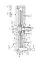
本発明の第1の実施の形態の成膜装置は、図1(図3のI−I’線に沿った断面図)〜図3に示すように、平面形状が概ね円形である扁平な真空容器(チャンバー)1と、この真空容器1内に設けられ、当該真空容器1の中心に回転中心を有する回転テーブル2と、を備えている。真空容器1は天板11が容器本体12から着脱できるように構成されている。この天板11は、真空容器1内が減圧されることにより、容器本体12の上面の周縁部にリング状に設けられたシール部材例えばOリング13を介して容器本体12側に引きつけられて気密状態を維持しているが、容器本体12から分離するときには図示しない駆動機構により上方に持ち上げられる。[First Embodiment]
The film forming apparatus according to the first embodiment of the present invention is a flat vacuum having a substantially circular planar shape as shown in FIG. 1 (cross-sectional view along the line II ′ in FIG. 3) to FIG. A container (chamber) 1 and a rotary table 2 provided in the vacuum container 1 and having a center of rotation at the center of the vacuum container 1 are provided. The vacuum vessel 1 is configured such that the
回転テーブル2は、中心部にて円筒形状のコア部21に固定され、このコア部21は、鉛直方向に伸びる回転軸22の上端に固定されている。回転軸22は真空容器1の底面部14を貫通し、その下端が当該回転軸22を鉛直軸回りにこの例では時計回りに回転させる回転機構である駆動部23に取り付けられている。そして、後述するように、回転テーブル2はこの駆動部23により、薄膜の成膜中において例えば100rpm〜240rpmで鉛直方向軸回りに回転できるように構成されている。回転軸22及び駆動部23は、上面が開口した筒状のケース体20内に収納されている。このケース体20はその上面に設けられたフランジ部分が真空容器1の底面部14の下面に気密に取り付けられており、ケース体20の内部雰囲気と外部雰囲気との気密状態が維持されている。 The rotary table 2 is fixed to a
回転テーブル2の表面部には、図2及び図3に示すように回転方向(周方向)に沿って複数枚例えば5枚の基板である半導体ウエハ(以下「ウエハ」という)Wを載置するための円形状の凹部24が設けられている。なお図3には便宜上1個の凹部24だけにウエハWを描いてある。ここで図4は、回転テーブル2を同心円に沿って切断しかつ横に展開して示す展開図であり、凹部24は、図4(a)に示すようにその直径がウエハWの直径よりも僅かに例えば4mm大きく、またその深さはウエハWの厚みと同等の大きさに設定されている。従ってウエハWを凹部24に落とし込むと、ウエハWの表面と回転テーブル2の表面(ウエハWが載置されない領域)とが揃うことになる。凹部24の底面には、ウエハWの裏面を支えて当該ウエハWを昇降させるための3本の昇降ピンが貫通する貫通孔(いずれも図示せず)が形成されている。
この凹部24は、ウエハWを位置決めして回転テーブル2の回転に伴なう遠心力により飛び出さないようにするためのものであり、本発明の基板載置領域に相当する部位である。As shown in FIGS. 2 and 3, a plurality of, for example, five semiconductor wafers (hereinafter referred to as “wafers”) W are placed on the surface of the
The
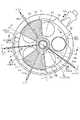
図2及び図3に示すように真空容器1には、回転テーブル2における凹部24の通過領域と各々対向する上位置に、第1の反応ガスノズル31及び第2の反応ガスノズル32と2本の分離ガスノズル41、42とが真空容器1の周方向(回転テーブル2の回転方向)に互いに間隔をおいて中心部から放射状に伸びている。この例では、後述の搬送口15から見て時計回りに第2の反応ガスノズル32、分離ガスノズル41、第1の反応ガスノズル31及び分離ガスノズル42がこの順に配列されている。これら反応ガスノズル31、32及び分離ガスノズル41、42は、例えば真空容器1の側周壁に取り付けられており、その基端部であるガス導入ポート31a、32a、41a、42aは当該側壁を貫通している。
これらのガスノズル31、32、41、42は、真空容器1の周壁部から真空容器1内に導入されている。As shown in FIGS. 2 and 3, the vacuum vessel 1 is separated into the first
These
第1の反応ガスノズル31及び第2の反応ガスノズル32は、夫々図示しない流量調整バルブなどを介して、夫々第1の反応ガス(処理ガス)であるTi(チタン)を含む反応ガス例えばTiCl4(塩化チタン)ガス及び第2の反応ガスであるN(窒素)を含む反応ガス例えばNH3(アンモニア)ガスの供給源(いずれも図示せず)に接続されている。また、分離ガスノズル41、42は、いずれも流量調整バルブなどを介して分離ガス(不活性ガス)であるN2(窒素)ガスが貯留されたガス供給源(図示せず)に接続されている。 The first
反応ガスノズル31、32には、下方側に反応ガスを吐出するための処理ガス供給口として例えば口径が0.3mmの吐出孔33が真下を向いてノズルの長さ方向に例えば2.5mmの間隔を置いて配列されている。また分離ガスノズル41、42には、下方側に分離ガスを吐出するための例えば口径が0.5mmの吐出孔40が真下を向いて長さ方向に例えば10mm程度の間隔を置いて穿設されている。反応ガスノズル31、32は夫々第1の反応ガス供給手段及び第2の反応ガス供給手段に相当し、分離ガスノズル41、42は分離ガス供給手段に相当する。また、反応ガスノズル31、32の下方領域は夫々TiCl4ガスをウエハWに吸着させるための第1の処理領域91及びNH3ガスをウエハWに吸着させるための第2の処理領域92となる。 The
既述の図1〜図4では省略しているが、反応ガスノズル31、32は、図5(a)に示すように、処理領域91、92における天井面45から離間してウエハWの近傍に夫々設けられており、ノズル31、32の長さ方向に沿ってこれらのノズル31、32を上方側から覆うと共に、下方側が開口するノズルカバー120を備えている。回転テーブル2の回転方向におけるノズルカバー120の両側面部は、下端部が水平方向に伸び出してフランジ状の整流部材121をなしている。この整流部材121は、処理領域91、92内への分離ガスの回り込み及びノズル31、32の上方側への反応ガスの舞い上がりを抑えるためのものであり、回転テーブル2の中心側から外周側に向かうにつれて、幅寸法が大きくなっている。そのため、図5(b)に示すように、これらのノズル31、32の上流側から各処理領域91、92に向かってくる分離ガスは、ノズルカバー120の上方領域を通って排気口61、62へと各々排気されていき、各処理領域91、92における反応ガスの濃度が高く保たれることになる。尚、この図5は、回転テーブル2の周方向に沿って装置を縦断して展開した図であり、成膜装置では処理領域91,92及び分離領域Dよりも外方領域に排気口61、62が設けられているが、各ガスの流れを示すために便宜上処理領域91,92及び分離領域Dと排気口61、62とを同一平面に示している。また、この整流部材121は、図5のように回転テーブル2の回転方向両側面に形成しても良いし、上流側及び下流側の一方だけに設けても良い。 Although omitted in FIGS. 1 to 4 described above, the
分離ガスノズル41、42は、第1の処理領域91と第2の処理領域92とを分離するための分離領域Dを形成するためのものであり、この分離領域Dにおける真空容器1の天板11には図2〜図4に示すように、回転テーブル2の回転中心を中心としかつ真空容器1の内周壁の近傍に沿って描かれる円を周方向に分割してなる、平面形状が扇型で下方に突出した凸状部4が設けられている。分離ガスノズル41、42は、この凸状部4における前記円の周方向中央にて当該円の半径方向に伸びるように形成された溝部43内に収められている。即ち分離ガスノズル41(42)の中心軸から凸状部4である扇型の両縁(回転テーブル2の回転方向上流側の縁及び下流側の縁)までの距離は同じ長さに設定されている。
なお、溝部43は、本実施形態では凸状部4を二等分するように形成されているが、他の実施形態においては、例えば溝部43から見て凸状部4における回転テーブル2の回転方向上流側が前記回転方向下流側よりも広くなるように溝部43を形成してもよい。The
In addition, although the
従って分離ガスノズル41、42における前記回転方向両側には、前記凸状部4の下面である例えば平坦な低い天井面44(第1の天井面)が存在し、この天井面44の前記回転方向両側には、当該天井面44よりも高い天井面45(第2の天井面)が存在することになる。この凸状部4の役割は、回転テーブル2との間に第1の反応ガス及び第2の反応ガスの侵入を阻止してこれら反応ガスの混合を阻止するための狭隘な空間である分離空間を形成することにある。
即ち、分離ガスノズル41を例にとると、回転テーブル2の回転方向上流側からNH3ガスが侵入することを阻止し、また回転方向下流側からTiCl4ガスが侵入することを阻止する。Accordingly, for example, a flat low ceiling surface 44 (first ceiling surface) that is the lower surface of the
That is, taking the
この例では直径300mmのウエハWを被処理基板としており、この場合凸状部4は、回転テーブル2の回転中心から140mm外周側に離れた部位(後述の突出部5との境界部位)においては、周方向の長さ(回転テーブル2と同心円の円弧の長さ)が例えば146mmであり、ウエハWの載置領域(凹部24)の最も外側部位においては、周方向の長さが例えば502mmである。なお図4(a)に示すように、当該外側部位において分離ガスノズル41(42)の両脇から夫々左右に位置する凸状部4の周方向の長さLでみれば、長さLは246mmである。 In this example, a wafer W having a diameter of 300 mm is used as a substrate to be processed. In this case, the
また図4(a)に示すように凸状部4の下面即ち天井面44における回転テーブル2の表面までの高さhは、例えば0.5mmから4mmに設定されている。そのため、分離領域Dの分離機能を確保するためには、回転テーブル2の回転数の使用範囲などに応じて、凸状部4の大きさや凸状部4の下面(第1の天井面44)と回転テーブル2の表面との高さhを例えば実験などに基づいて設定することになる。なお分離ガスとしては、窒素(N2)ガスに限られずアルゴン(Ar)ガスなどの不活性ガスなどを用いることができる。 Further, as shown in FIG. 4A, the height h from the lower surface of the
天板11の下面には、回転テーブル2におけるコア部21よりも外周側の部位と対向するようにかつ当該コア部21の外周に沿って突出部5が設けられている。この突出部5は凸状部4における回転テーブル2の回転中心側の部位と連続して形成されており、その下面が凸状部4の下面(天井面44)と同じ高さに形成されている。図2及び図3は、前記天井面45よりも低くかつ分離ガスノズル41、42よりも高い位置にて天板11を水平に切断して示している。なお突出部5と凸状部4とは、必ずしも一体であることに限られるものではなく、別体であってもよい。 A projecting
真空容器1の天板11の下面、つまり回転テーブル2のウエハ載置領域(凹部24)から見た天井面は既述のように第1の天井面44とこの天井面44よりも高い第2の天井面45とが周方向に存在するが、図1では、高い天井面45が設けられている領域についての縦断面を示しており、図6では、低い天井面44が設けられている領域についての縦断面を示している。扇型の凸状部4の周縁部(真空容器1の外縁側の部位)は図2及び図6に示されているように回転テーブル2の外端面に対向するようにL字型に屈曲して屈曲部46を形成している。扇型の凸状部4は天板11側に設けられていて、容器本体12から取り外せるようになっていることから、前記屈曲部46の外周面と容器本体12との間には僅かに隙間がある。この屈曲部46も凸状部4と同様に両側から反応ガスが侵入することを防止して、両反応ガスの混合を防止する目的で設けられており、屈曲部46の内周面と回転テーブル2の外端面との隙間、及び屈曲部46の外周面と容器本体12との隙間は、回転テーブル2の表面に対する天井面44の高さhと同様の寸法に設定されている。この例においては、回転テーブル2の表面側領域からは、屈曲部46の内周面が真空容器1の内周壁を構成していると見ることができる。 The lower surface of the
容器本体12の内周壁は、分離領域Dにおいては図6に示すように前記屈曲部46の外周面と接近して垂直面に形成されているが、分離領域D以外の部位においては、図1に示すように例えば回転テーブル2の外端面と対向する部位から底面部14に亘って縦断面形状が矩形に切り欠かれて外方側に窪んだ構造になっている。この窪んだ部位における既述の第1の処理領域91及び第2の処理領域92に連通する領域を夫々第1の排気領域E1及び第2の排気領域E2と呼ぶことにすると、これらの第1の排気領域E1及び第2の排気領域E2の底部には、図3に示すように、夫々第1の排気口61及び第2の排気口62が形成されている。図1に示すように、これら排気口61、62は、各々排気路63を介して真空排気手段である例えば真空ポンプ64に接続されている。なお図1中、65は圧力調整手段であり、各々の排気路63毎に設けられている。 As shown in FIG. 6, the inner peripheral wall of the container
既述のように、排気口61、62は、分離領域Dの分離作用が働くように、平面で見たときに前記分離領域Dの前記回転方向両側に設けられている。詳しく言えば、回転テーブル2の回転中心から見て第1の処理領域91とこの第1の処理領域91に対して例えば回転方向下流側に隣接する分離領域Dとの間に第1の排気口61が形成され、回転テーブル2の回転中心から見て第2の処理領域92とこの第2の処理領域92に対して例えば回転方向下流側に隣接する分離領域Dとの間に第2の排気口62が形成されており、これらの排気口61、62は、夫々各反応ガス(TiCl4ガス及びNH3ガス)の排気を専用に(個別に)行うように配置されている。この例では一方の排気口61は、第1の反応ガスノズル31とこの反応ガスノズル31に対して前記回転方向下流側に隣接する分離領域Dの第1の反応ガスノズル31側の縁の延長線との間に設けられ、また他方の排気口61は、第2の反応ガスノズル32とこの反応ガスノズル32に対して前記回転方向下流側に隣接する分離領域Dの第2の反応ガスノズル32側の縁の延長線との間に設けられている。即ち、第1の排気口61は、図3中に一点鎖線で示した回転テーブル2の中心と第1の処理領域91とを通る直線L1と、回転テーブル2の中心と前記第1の処理領域91の下流側に隣接する分離領域Dの上流側の縁を通る直線L2との間に設けられ、第2の排気口62は、この図3に二点鎖線で示した回転テーブル2の中心と第2の処理領域92とを通る直線L3と、回転テーブル2の中心と前記第2の処理領域92の下流側に隣接する分離領域Dの上流側の縁を通る直線L4との間に位置している。 As described above, the
この例では、排気口61、62を回転テーブル2よりも低い位置に設けることで真空容器1の内周壁と回転テーブル2の周縁との間の隙間から排気するようにしているが、真空容器1の底面部に設けることに限られず、真空容器1の側壁に排気口61、62を設けてもよい。 In this example, the
前記回転テーブル2と真空容器1の底面部14との間の空間には、図1に示すように加熱手段であるヒータユニット7が設けられており、回転テーブル2を介して回転テーブル2上のウエハWをプロセスレシピで決められた温度に加熱するように構成されている。前記回転テーブル2の周縁付近の下方側には、回転テーブル2の上方空間から排気領域Eに至るまでの雰囲気とヒータユニット7が置かれている雰囲気とを区画するために、ヒータユニット7を全周に亘って囲むようにカバー部材71が設けられている。このカバー部材71は上縁が外側に屈曲されてフランジ形状に形成され、その屈曲面と回転テーブル2の下面との間の隙間を小さくして、カバー部材71内に外方からガスが侵入することを抑えている。 In the space between the
ヒータユニット7が配置されている空間よりも回転中心寄りの部位における底面部14は、回転テーブル2の下面の中心部付近、コア部21に接近してその間は狭い空間になっており、また当該底面部14を貫通する回転軸22の貫通穴についてもその内周面と回転軸22との隙間が狭くなっていて、これら狭い空間は前記ケース体20内に連通している。そして前記ケース体20にはパージガスであるN2ガスを前記狭い空間内に供給してパージするためのパージガス供給管72が設けられている。また真空容器1の底面部14には、ヒータユニット7の下方側位置にて周方向の複数部位に、ヒータユニット7の配置空間をパージするためのパージガス供給管73が設けられている。 The
このようにパージガス供給管72、73を設けることにより、ケース体20内からヒータユニット7の配置空間に至るまでの空間がN2ガスでパージされ、このパージガスが回転テーブル2とカバー部材71との間の隙間から排気領域Eを介して排気口61、62に排気される。これによって既述の第1の処理領域91と第2の処理領域92との一方から回転テーブル2の下方を介して他方にTiCl4ガスあるいはNH3ガスの回り込みが防止されるため、このパージガスは分離ガスの役割も果たしている。 By providing the purge
また真空容器1の天板11の中心部には分離ガス供給管51が接続されていて、天板11とコア部21との間の空間52に分離ガスであるN2ガスを供給するように構成されている。この空間52に供給された分離ガスは、前記突出部5と回転テーブル2との狭い隙間50を介して回転テーブル2のウエハ載置領域側の表面に沿って周縁に向けて吐出されることになる。この突出部5で囲まれる空間には分離ガスが満たされているので、第1の処理領域91と第2の処理領域92との間で回転テーブル2の中心部を介して反応ガス(TiCl4ガス及びNH3ガス)が混合することを防止している。 Further, a separation
更に真空容器1の側壁には図2及び図3に示すように外部の搬送アーム10と回転テーブル2との間でウエハWの受け渡しを行うための搬送口15が形成されており、この搬送口15は図示しないゲートバルブにより開閉されるようになっている。また回転テーブル2におけるウエハ載置領域である凹部24はこの搬送口15に臨む位置にて搬送アーム10との間でウエハWの受け渡しが行われることから、回転テーブル2の下方側において当該受け渡し位置に対応する部位に、凹部24を貫通してウエハWを裏面から持ち上げるための受け渡し用の昇降ピン16の昇降機構(図示せず)が設けられる。 Further, as shown in FIGS. 2 and 3, a
また、この成膜装置は、既述の図1に示したように、装置全体の動作のコントロールを行うためのコンピュータからなる制御部80を備えており、制御部80は、図示しないCPU、メモリ、処理プログラム及びワークメモリを備えている。このメモリには、ウエハWに対して行う処理の種別毎に、ウエハWの加熱温度、各反応ガスの流量、真空容器1内の処理圧力及び回転テーブル2の回転数などのレシピ(処理条件)が記憶されており、ウエハWに対して反応ガスを供給して薄膜の成膜処理を行う時には、回転テーブル2の回転数は、薄膜を速やかに成膜すると共に、後述の実施例に示すように、薄膜の表面モフォロジーを良好にする(表面の面状態を平滑にする)ために、例えば100rpm〜240rpmに設定される。前記処理プログラムは、ハードディスク、コンパクトディスク、光磁気ディスク、メモリカード、フレキシブルディスクなどの記憶媒体85から制御部80内にインストールされる。 Further, as shown in FIG. 1 described above, the film forming apparatus includes a control unit 80 including a computer for controlling the operation of the entire apparatus. The control unit 80 includes a CPU and a memory (not shown). And a processing program and a work memory. In this memory, recipes (processing conditions) such as the heating temperature of the wafer W, the flow rate of each reaction gas, the processing pressure in the vacuum vessel 1 and the number of rotations of the rotary table 2 are determined for each type of processing performed on the wafer W. Is stored, and when the thin film is formed by supplying the reaction gas to the wafer W, the rotation speed of the
次に、上述の第1の実施の形態の作用について、図7及び図8を参照して説明する。先ず、図示しないゲートバルブを開き、外部から搬送アーム10により搬送口15を介してウエハWを回転テーブル2の凹部24内に受け渡す。この受け渡しは、凹部24が搬送口15に臨む位置に停止したときに、凹部24の底面の貫通孔を介して真空容器1の底部側から昇降ピン16が昇降することにより行われる。このようなウエハWの受け渡しを回転テーブル2を間欠的に回転させて行い、回転テーブル2の5つの凹部24内に夫々ウエハWを載置する。続いて、ゲートバルブを閉じて圧力調整手段65の開度を全開にして真空容器1内を引き切りの状態にして、回転テーブル2を例えば100rpmで時計回りに回転させると共に、ヒータユニット7によりウエハW(回転テーブル2)をTiN(チタンナイトライド、窒化チタン)の結晶化する温度例えば250℃以上の温度この例では400℃に加熱する。 Next, the operation of the above-described first embodiment will be described with reference to FIGS. First, a gate valve (not shown) is opened, and the wafer W is transferred from the outside to the
次いで、真空容器1内の圧力値が所定の値例えば1066.4Pa(8Torr)となるように圧力調整手段65の開度を調整する。また、第1の反応ガスノズル31から例えば100sccmでTiCl4ガスを供給すると共に、第2の反応ガスノズル32から例えば5000sccmでNH3ガスを供給する。更に、分離ガスノズル41、42からいずれも10000sccmでN2ガスを供給すると共に、分離ガス供給管51及びパージガス供給管72、73からも所定の流量でN2ガスを真空容器1内に供給する。 Next, the opening degree of the pressure adjusting means 65 is adjusted so that the pressure value in the vacuum vessel 1 becomes a predetermined value, for example, 1066.4 Pa (8 Torr). Further, TiCl4 gas is supplied from the first
そして、回転テーブル2の回転により、ウエハWが第1の処理領域91を通過すると、図7(a)に示すように、当該ウエハWの表面にはTiCl4ガスが吸着する。この時、回転テーブル2を既述のように高速で回転させると共に反応ガスの流量や処理圧力を既述のように設定しているので、ウエハW上のTiCl4の吸着膜151の膜厚t1は、TiCl4ガスの吸着量が飽和するまで例えばウエハWをTiCl4ガスの雰囲気中に静置した時の飽和膜厚t0よりも薄くなる。このようにTiCl4ガスの吸着膜厚t1を飽和膜厚t0よりも薄く形成するにあたって、既述のように回転テーブル2の回転中心から外周側に向かって回転テーブル2と水平に第1の反応ガスノズル31をウエハWに近接させて設けると共に、吐出孔33を当該ガスノズル31の長さ方向に亘って等間隔に設けていることから、更には各処理領域91、92間に分離領域Dを各々設けて真空容器1内におけるガス流の安定化を図っていることから、TiCl4ガスがウエハW上に均一に供給されて、吸着膜151の膜厚がウエハWの面内に亘って均一となる。 Then, when the wafer W passes through the
次いで、このウエハWが第2の処理領域92を通過すると、図7(b)に示すように、ウエハWの表面の吸着膜151が窒化されてTiN膜152の分子層が1層あるいは複数層生成する。このTiN膜152は、結晶化に伴う原子や分子のマイグレーション(移動)によって、グレインサイズが大きくなろうと(粒成長しようと)する。この粒成長が進行するにつれてTiN膜152の表面モフォロジーが悪化して(表面状態が粗くなって)いくことになるが、既述のように回転テーブル2を高速で回転させているので、表面にTiN膜152が形成されたウエハWは、その後第1の処理領域91を直ぐに通過して、続いて第2の処理領域92に速やかに到達する。即ち、ウエハWの表面へのTiCl4ガスの吸着と、このTiCl4ガスの窒化処理と、からなる処理のサイクル間の時間(TiN膜152の結晶化が進行する時間)が極めて短く設定されていると言える。そのため、図7(c)、(d)に示すように、下層側のTiN膜152の結晶化の進行する前に上層側にTiN膜153が積層されることによって、下層側のTiN膜152における原子や分子の移動が上層側の反応生成物であるTiN膜153によって阻害され、いわば下層側のTiN膜152の表面状態(粒成長)が上層側のTiN膜153によって規制されていることになる。また、吸着膜151の膜厚t1が既述のように薄く形成されているので、TiN膜152においてTiN粒子の結晶化が起こったとしても、成長後のグレインサイズ(表面モフォロジーの悪化の度合い)が小さく抑えられる。従って、この下層側のTiN膜152は、後述の実施例にて説明するように、CVD(Chemical Vapor Deposition)法やサイクル間の時間が長い従来のALD(Atomic Layer Deposition)法などにより成膜した場合と比較して、グレインサイズが極めて小さく、且つ表面状態が平滑となる。 Next, when the wafer W passes through the
また、上層側のTiN膜153は、続いて速やかにウエハWが処理領域91、92を通過するので、同様に更に上層側に形成されるTiN膜によって原子や分子の移動が規制されることになる。こうしてウエハWが第1の処理領域91と第2の処理領域92とをこの順番で交互に複数回通過することにより、既述のグレインサイズが極めて小さく表面が平滑な反応生成物が順次積層されてTiN膜の薄膜が形成される。この薄膜は、既述のように回転テーブル2を高速で回転させていることから、例えば従来のALD法よりも速やかに成膜される。この時の成膜速度は、各反応ガスの供給量や真空容器1内の処理圧力などに応じて変化するが、一例を挙げると例えば5.47nm/min程度となる。 In addition, since the
この時、分離領域DにおいてN2ガスを供給し、また中心部領域Cにおいても分離ガスであるN2ガスを供給しているので、既述のように回転テーブル2を高速で回転させている場合であっても、図8に示すように、TiCl4ガスとNH3ガスとが混合しないように各ガスが排気されることとなる。また、分離領域Dにおいては、屈曲部46と回転テーブル2の外端面との間の隙間が既述のように狭くなっているので、TiCl4ガスとNH3ガスとは、回転テーブル2の外側を介しても混合しない。従って、第1の処理領域91の雰囲気と第2の処理領域92の雰囲気とが完全に分離され、TiCl4ガスは排気口61に、またNH3ガスは排気口62に夫々排気される。この結果、TiCl4ガス及びNH3ガスが雰囲気中においてもウエハW上においても混じり合うことがない。また、回転テーブル2の下方側をN2ガスによりパージしているため、排気領域Eに流入したガスが回転テーブル2の下方側を潜り抜けて、例えばTiCl4ガスがNH3ガスの供給領域に流れ込むといったおそれは全くない。こうして成膜処理が終了すると、ガスの供給を停止して真空容器1内を真空排気し、その後回転テーブル2の回転を停止して各ウエハWを搬入時と逆の動作によって順次搬送アーム10により搬出する。
ここで処理パラメータの一例について記載しておくと、真空容器1の中心部の分離ガス供給管51からのN2ガスの流量は例えば5000sccmである。また1枚のウエハWに対する反応ガス供給のサイクル数、即ちウエハWが処理領域91、92の各々を通過する回数は目標膜厚に応じて変わるが、多数回例えば600回である。At this time, since the N2 gas is supplied in the separation region D and the N2 gas which is the separation gas is also supplied in the central region C, the rotary table 2 is rotated at a high speed as described above. Even if it exists, as shown in FIG. 8, each gas will be exhausted so that TiCl4 gas and NH3 gas may not mix. In the separation region D, since the gap between the
Here, an example of the processing parameters will be described. The flow rate of the N2 gas from the separation
上述の実施の形態によれば、真空容器1内の回転テーブル2上にウエハWを載置して、このウエハWに対して反応ガスを供給して真空雰囲気下においてチタンナイトライド膜の成膜を行うにあたり、薄膜の成膜処理を行う時に、回転テーブル2と各ガスノズル31、32、41、42とを100rpm以上で相対的に真空容器1の周方向に回転させるようにしている。そのため、反応ガスの供給サイクル(反応生成物の成膜サイクル)を高速で行うことができるので、薄膜を速やかに形成することができ、スループットを高めることができる。また、サイクル間の時間が極めて短いので、基板の表面に生成した反応生成物の結晶化による粒子径の粗大化が進行する前に次の反応生成物の層を上層側に積層して、いわば上層側の反応生成物により下層側の反応生成物における原子や分子のマイグレーション(移動)を規制することができるため、結果として表面形状を悪化させるマイグレーションを抑制することができ、従って従来のCVD法やサイクル間の時間が長いALD法によって成膜した薄膜よりも表面形状が平滑な薄膜を得ることができる。 According to the above-described embodiment, the wafer W is placed on the
そのため、このTiN膜を次世代キャパシター電極例えばZrO(酸化ジルコニウム)、TiO(酸化チタン)、TaO(酸化タンタル)などのバリア膜として用いた場合には、当該電極における電荷の集中を抑制し、良好な電気的特性を得ることができる。また、半導体装置の多層構造において、上層側の配線層と下層側の配線層との間の層間絶縁膜にこれら配線層同士を接続するアルミニウムなどの金属層を埋め込むためのコンタクトホールなどの凹部に、層間絶縁膜への金属層の拡散を防止するためのバリア膜としてこのTiN膜を用いる時には、このコンタクトホールのアスペクト比が50程度まで大きい場合であっても、同様に表面が平滑で被覆性の高い薄膜を速やかに得ることができる。 Therefore, when this TiN film is used as a barrier film such as a next-generation capacitor electrode such as ZrO (zirconium oxide), TiO (titanium oxide), TaO (tantalum oxide), etc. Electrical characteristics can be obtained. In a multilayer structure of a semiconductor device, a recess such as a contact hole for embedding a metal layer such as aluminum connecting the wiring layers in an interlayer insulating film between an upper wiring layer and a lower wiring layer is used. When this TiN film is used as a barrier film for preventing the diffusion of the metal layer into the interlayer insulating film, the surface is smooth and covering even when the aspect ratio of the contact hole is large up to about 50 Can be obtained quickly.
また、ウエハW上に吸着させる吸着膜151の膜厚t1について、飽和膜厚t0よりも薄くしているので、TiN粒子の結晶化が起こったとしても成長するグレインのサイズを極めて小さく抑えることができる。即ち、本発明では回転テーブル2を高速で回転させることにより、吸着膜151の膜厚t1を薄く(グレインサイズを小さく)制御していると言える。 In addition, since the film thickness t1 of the
一方、回転テーブル2の回転数を低速例えば30rpm以下に設定してTiN膜152の成膜処理を行った場合には、図9(a)に示すように、例えば吸着膜151の膜厚t2がほぼ飽和膜厚t0と等しくなり、薄膜の表面モフォロジーが悪化することになる。つまり、同図(b)に示すように、この吸着膜151の形成されたウエハWに対してNH3ガスを供給してTiN膜152が生成すると、TiCl4の吸着膜151の形成とこの吸着膜151の窒化とからなる処理サイクル間の時間が長く取られることになるので、同図(c)に示すように、TiN膜152の上層に次のTiN膜153が形成されるまでの間に、当該TiN膜152中においてTiN粒子の結晶化が進行することによって原子や分子のマイグレーション(移動)が起こり、表面モフォロジーが悪化してしまう。この時、吸着膜151の膜厚t2が既述の膜厚t1よりも厚くなっていることから、結晶化によって成長する粒子のサイズ(表面状態の悪化)もこの膜厚t2に応じて大きくなる場合がある。 On the other hand, when the
そのため、この表面状態の荒れたTiN膜152の表面にTiCl4ガスが供給されると、図9(d)に示すように、上層側の吸着膜151は下層側のTiN膜152の表面に倣って形成されるので、当該吸着膜151の表面についても同様に荒れた状態となる。その後、この上層側の吸着膜151にNH3ガスが供給されると、同様に上層側のTiN膜153についても結晶化が進行するので、表面がより一層荒れてしまう。こうして順次積層するTiN膜の各々について結晶化が進行することにより、得られる薄膜の表面は極めて凹凸の大きな状態となってしまう。従って、回転テーブル2の回転数をこのように低速に設定して成膜処理を行った場合には、表面モフォロジーを制御することは極めて困難である。また、回転テーブル2の回転数を遅く設定すると、成膜速度についても遅くなってしまう。 Therefore, when TiCl4 gas is supplied to the surface of the
以上のことから、本発明では、回転テーブル2の回転数を高速に設定してTiN膜の成膜を行うことにより、表面モフォロジーの良好なTiN膜を速やかに成膜できることが分かる。ここで、本発明の成膜装置では、回転テーブル2上のウエハWに対向させて各反応ガスノズル31、32を設けていることから、例えば反応ガスの流量を多くすることにより、あるいは処理圧力を高く設定することにより、ウエハW上に吸着する反応ガスの吸着量が飽和するようにしても良い。この場合においても、回転テーブル2を高速で回転させているので、TiN膜152の結晶化が進行する前に続く上層側のTiN膜153を成膜することができ、良好な表面モフォロジーの薄膜を得ることができるし、また各反応サイクルにおける膜厚を稼ぐことができるので、スループットを更に高めることができる。このように反応ガスの供給量を増やしたり処理圧力を高めたりした場合であっても、各反応ガスは同様に個別に排気される。 From the above, it can be seen that in the present invention, a TiN film having a good surface morphology can be rapidly formed by setting the rotation speed of the
既述の第1の反応ガスとしては、上述の例の他に、Tiを含むガス例えばTDMAT(テトラキスジメチルアミノチタン)ガスなどを用いても良いし、第2の反応ガスとしては、NH3ガスをラジカル化させて用いても良い。また、回転テーブル2の回転数としては、高すぎると例えば薄膜の被覆性が低くなるので、例えば240rpm以下であることが好ましい。即ち、後述の実施例においてTiN膜を成膜する実験を行った時には、回転テーブル2の回転数が240rpmでも良好な被覆性となっていたため、少なくとも240rpm以下であれば良好な被覆性が得られると言える。 As the first reaction gas described above, in addition to the above example, a gas containing Ti, such as TDMAT (tetrakisdimethylaminotitanium) gas, may be used. As the second reaction gas, NH3 gas is used. It may be used after radicalization. Further, if the rotational speed of the
[第2の実施の形態]
第1の実施の形態では、TiCl4ガスの吸着膜151の形成と、この吸着膜151の窒化によるTiN膜152の形成と、からなる成膜サイクルを複数回繰り返して薄膜を成膜するようにしたが、例えばTiN膜152に不純物が含まれている場合などには、成膜サイクルの間にTiN膜152に対してプラズマ処理を行うようにしても良い。このようにプラズマ処理を行う場合の成膜装置の一例について、第2の実施の形態として図10〜図12を参照して以下に説明する。[Second Embodiment]
In the first embodiment, a thin film is formed by repeating a film formation cycle consisting of the formation of the
この例では、例えば搬送口15よりも回転テーブル2の回転方向上流側に既述の第2の反応ガスノズル32が設けられており、第2の反応ガスノズル32と当該第2の反応ガスノズル32における回転テーブル2の回転方向下流側の分離領域Dとの間には、ウエハWに対してプラズマ処理を行うための活性化ガスインジェクター220が設けられている。この活性化ガスインジェクター220は、回転テーブル2の外周側から回転中心側に向かって当該回転テーブル2に対して水平に伸びるガス導入ノズル34及び一対のシース管(図示せず)と、これらガス導入ノズル34及び一対のシース管が配置される領域を長さ方向に亘って上方側から覆うように設けられ、既述のノズルカバー120と同様に構成された例えば石英からなるカバー体221と、を備えている。図中222は、既述の整流部材121と同様の寸法に設定された気流規制面222であり、223は、真空容器1の天板11からカバー体221を吊り下げるために当該カバー体221の長さ方向に沿って設けられた支持体である。尚、図10中37は、シース管の基端部(真空容器1の内壁側)に接続された保護管である。 In this example, for example, the second
真空容器1の外部には、高周波電源180が設けられており、整合器181を介してシース管内に埋設された図示しない電極に対して例えば13.56MHz、例えば1500W以下の高周波電力を供給できるように構成されている。ガス導入ノズル34は、側方側に長さ方向に沿って複数箇所に形成されたガス孔341を介して、プラズマ発生用の処理ガス例えばNH3ガス及びH2ガスの少なくとも一方が真空容器1の外部からシース管に向かって水平に吐出されるように構成されている。 A high frequency power supply 180 is provided outside the vacuum vessel 1 so that high frequency power of, for example, 13.56 MHz, for example, 1500 W or less can be supplied to an electrode (not shown) embedded in the sheath tube via the
この第2の実施の形態において成膜処理を行う場合には、各ガスノズル31、32、41、42から各ガスを真空容器1内に供給すると共に、ガス導入ノズル34からプラズマ生成用の処理ガス例えばNH3ガスを所定の流量例えば5000sccmで真空容器1に供給する。また、図示しない高周波電源から電極36a、36bに対して所定の値の電力例えば400Wの高周波を供給する。 When the film forming process is performed in the second embodiment, each gas is supplied from the
活性化ガスインジェクター220では、ガス導入ノズル34からシース管35a、35bに向かって吐出されたNH3ガスは、これらのシース管35a、35b間に供給される高周波によって活性化されてイオンなどの活性種となり、この活性種(プラズマ)が下方に向かって吐出される。図13(a)、(b)に示すように、表面に吸着膜151が形成され、続いてこの吸着膜151が窒化されてTiN膜152の成膜されたウエハWは、活性化ガスインジェクター220の下方領域に到達すると、同図(c)に示すようにプラズマに曝されて、例えば表面のTiN膜152にCl(塩素)などの不純物が含まれている場合には、この不純物が膜中から排出されていく。そして、既述の第1の実施の形態と同様に、同図(d)に示すように、その後当該TiN膜152の上層側に次のTiN膜153が速やかに積層されて、下層側のTiN膜152における原子や分子の移動が規制される。こうして吸着膜151の生成と、この吸着膜151の窒化によるTiN膜152の生成と、プラズマによる不純物の低減(除去)と、をこの順序で複数回繰り返すことにより、不純物の極めて少なく、且つ表面が平滑な薄膜が速やかに成膜される。 In the activated
この第2の実施の形態によれば、既述の第1の実施の形態の効果に加えて、以下の効果がある。即ち、ウエハWに対してプラズマ処理を行うことにより薄膜中の不純物の量を低減できるので、電気的特性を向上させることができる。また、真空容器1の内部において成膜サイクルを行う度に改質処理を行っているので、いわば回転テーブル2の周方向においてウエハWが各処理領域91、92を通過する経路の途中において成膜処理に干渉しないように改質処理を行っているので、例えば薄膜の成膜が完了した後で改質処理を行うよりも短時間で改質処理を行うことができる。
また、既述の例においては、ガス供給系(ノズル31、32、41、42)に対して回転テーブル2を回転させるようにしたが、回転テーブル2に対してガス供給系を周方向に回転させる構成としても良い。According to the second embodiment, in addition to the effects of the first embodiment described above, there are the following effects. That is, by performing plasma treatment on the wafer W, the amount of impurities in the thin film can be reduced, so that the electrical characteristics can be improved. Further, since the reforming process is performed every time the film forming cycle is performed inside the vacuum vessel 1, the film is formed in the middle of the path through which the wafer W passes through the
In the example described above, the rotary table 2 is rotated with respect to the gas supply system (
続いて、本発明の効果を確認するために行った実験について説明する。
(実験例1)
先ず、回転テーブル2の回転数を以下に示すように種々変えてTiN膜の成膜を行い、得られたTiN膜の表面をSEM(電子顕微鏡)を用いて観察した。尚、その他の成膜条件例えば反応ガスの供給量や処理圧力などについては、各実験例において同じ条件としたため、説明を省略する。また、ウエハWの加熱温度としては250℃以上例えば400℃とした。
(回転テーブル2の回転数:rpm)
比較例1:30
実施例1:100、240Subsequently, an experiment conducted for confirming the effect of the present invention will be described.
(Experimental example 1)
First, a TiN film was formed by changing the number of revolutions of the
(Rotation speed of rotary table 2: rpm)
Comparative Example 1:30
Example 1: 100, 240
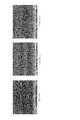
(実験結果)
その結果、図14に得られたSEM写真を示すように、比較例1では表面状態が粗く、従来のCVD法やSFD法を用いて成膜した面状態に近くなっていた。既述のように、TiNは250℃以上で結晶化するため、この実験における加熱温度において特にTiN粒子の結晶化を妨げない場合には、このようにTiN粒子の結晶化に起因する凹凸が膜表面に現れると考えられる。
一方、実施例1に示すように、回転テーブル2の回転数を高くして100rpmとした場合には、TiN膜の表面モフォロジーが向上し、更に240rpmでは極めて表面が平滑になることが分かった。従って、回転テーブル2を高速で回転させることによって、既述のように成膜サイクル間の時間が短くなり、上層側のTiN膜により下層側のTiN膜の結晶化を抑制できることが分かった。(Experimental result)
As a result, as shown in the SEM photograph obtained in FIG. 14, in Comparative Example 1, the surface state was rough, and it was close to the surface state formed using the conventional CVD method or SFD method. As described above, since TiN is crystallized at 250 ° C. or higher, in the case where the crystallization of TiN particles is not particularly disturbed at the heating temperature in this experiment, the unevenness caused by the crystallization of TiN particles is thus formed in the film. It appears to appear on the surface.
On the other hand, as shown in Example 1, it was found that when the rotation speed of the
(実験例2)
次いで、実験例1と同じ条件にて成膜した各サンプルについて、AFM(原子間力顕微鏡)を用いてTiN膜の表面粗さを測定した。尚、測定長としては10nmとした。
その結果、図15に示すように、回転テーブル2の回転数が30rpmの場合には表面粗さが2nm程度となっていたが、100rpm以上では0.5nm程度もの小さい値となっていた。(Experimental example 2)
Next, the surface roughness of the TiN film was measured using AFM (atomic force microscope) for each sample formed under the same conditions as in Experimental Example 1. The measurement length was 10 nm.
As a result, as shown in FIG. 15, the surface roughness was about 2 nm when the rotation speed of the
D 分離領域
E 排気領域
1 真空容器
W ウエハ
31、32 反応ガスノズル
41、42 分離ガスノズル
61、62 排気口
91、92 処理領域
151 吸着膜
152 TiN膜
153 TiN膜D Separation area E Exhaust area 1 Vacuum
Claims (9)
Translated fromJapanese前記真空容器内に設けられ、基板を載置するための基板載置領域が設けられたテーブルと、
前記真空容器の周方向に互いに離れて設けられ、前記テーブル上の基板に前記第1の反応ガス及び前記第2の反応ガスを夫々供給するための第1の反応ガス供給手段及び第2の反応ガス供給手段と、
前記第1の反応ガスが供給される第1の処理領域と前記第2の反応ガスが供給される第2の処理領域との間に設けられ、両反応ガスの混合を防止するための分離領域と、
前記第1の処理領域と前記第2の処理領域とを基板がこの順番で位置するように、前記第1の反応ガス供給手段及び前記第2の反応ガス供給手段と前記テーブルとを前記真空容器の周方向に相対的に回転させる回転機構と、
前記真空容器内を真空排気する真空排気手段と、
前記基板への成膜時に、前記第1の反応ガス供給手段及び前記第2の反応ガス供給手段と前記テーブルとを前記回転機構を介して100rpm以上で回転させる制御部と、
前記テーブル上の基板に対してNH3ガスまたはH2ガスの少なくとも一方のガスを供給するためのガスインジェクターと、
このガスインジェクターから供給されるガスをプラズマ化してプラズマを発生させるために高周波電力が供給される導電体と、を備え、
この導電体及び前記ガスインジェクターからなる構成は、前記回転機構により、前記第1の反応ガス供給手段及び前記第2の反応ガス供給手段と共に前記テーブルに対して相対的に回転するように構成され、前記相対的な回転時に前記プラズマが前記第2の処理領域と前記第1の処理領域との間において基板に供給されるように配置されていることを特徴とする成膜装置。In a film forming apparatus for forming a titanium nitride film by sequentially supplying a first reaction gas containing Ti and a second reaction gas containing N to the surface of a substrate in a vacuum vessel,
A table provided in the vacuum vessel and provided with a substrate placement region for placing a substrate;
First reaction gas supply means and second reaction for supplying the first reaction gas and the second reaction gas to the substrate on the table, which are provided apart from each other in the circumferential direction of the vacuum vessel. Gas supply means;
A separation region provided between the first processing region to which the first reaction gas is supplied and the second processing region to which the second reaction gas is supplied to prevent mixing of both reaction gases When,
The first reaction gas supply means, the second reaction gas supply means, and the table are arranged in the vacuum container so that the substrate is positioned in this order in the first processing area and the second processing area. A rotation mechanism that rotates relative to the circumferential direction of
Evacuation means for evacuating the inside of the vacuum vessel;
A control unit that rotates the first reaction gas supply unit, the second reaction gas supply unit, and the table at 100 rpm or more through the rotation mechanism during film formation on the substrate;
A gas injector for supplying at least one of NH3 gas and H2 gas to the substrate on the table;
A conductor supplied with high-frequency power in order to generate plasma by converting the gas supplied from the gas injector into plasma,
The structure composed of the conductor and the gas injector is configured to rotate relative to the table together with the first reaction gas supply unit and the second reaction gas supply unit by the rotation mechanism. The film forming apparatus, wherein the plasma is arranged to be supplied to the substrate between the second processing region and the first processing region during the relative rotation .
基板を載置するための基板載置領域が設けられたテーブル上に基板を載置する工程と、
次いで、前記真空容器の周方向に互いに離れて設けられた第1の反応ガス供給手段及び第2の反応ガス供給手段から、前記テーブルの表面に対して夫々前記第1の反応ガス及び前記第2の反応ガスを供給する工程と、
前記テーブル上の基板に対してガスインジェクターからNH3ガスまたはH2ガスの少なくとも一方のガスを供給すると共に、導電体に高周波電力を供給することによりこのガスをプラズマ化してプラズマを発生させる工程と、
前記第1の反応ガスが供給される第1の処理領域と前記第2の反応ガスが供給される第2の処理領域との間に設けられた分離領域において両反応ガスの混合を防止する工程と、
前記第1の処理領域と前記第2の処理領域と前記プラズマが供給される領域とを基板がこの順番で位置するように、前記第1の反応ガス供給手段、前記第2の反応ガス供給手段、前記ガスインジェクター及び前記導電体と前記テーブルとを相対的に前記真空容器の周方向に100rpm以上で回転させる工程と、
前記真空容器内を真空排気する工程と、を含むことを特徴とする成膜方法。In a film forming method for forming a titanium nitride film by sequentially supplying a first reaction gas containing Ti and a second reaction gas containing N to the surface of a substrate in a vacuum vessel,
Placing a substrate on a table provided with a substrate placement area for placing the substrate;
Next, from the first reaction gas supply means and the second reaction gas supply means provided apart from each other in the circumferential direction of the vacuum vessel, the first reaction gas and the second reaction gas are respectively applied to the surface of the table. Supplying a reactive gas of
Supplying at least one of NH3 gas or H2 gas from a gas injector to the substrate on the table, and generating a plasma by converting the gas into plasma by supplying high-frequency power to the conductor;
A step of preventing mixing of both reaction gases in a separation region provided between a first processing region to which the first reaction gas is supplied and a second processing region to which the second reaction gas is supplied When,
The first reactive gas supply meansand the second reactive gas supply means so that the substrate is positioned in this order in the first processing region, the second processing region, and the region to which theplasma is supplied.The step of rotating thegas injector and the conductor and the table relatively in the circumferential direction of the vacuum vessel at 100 rpm or more;
And evacuating the inside of the vacuum vessel.
前記プログラムは、請求項5ないし8のいずれか一つに記載の成膜方法を実施するようにステップ群が組まれていることを特徴とする記憶媒体。A memory for storing a program used in a film forming apparatus for forming a titanium nitride film by sequentially supplying a first reaction gas containing Ti and a second reaction gas containing N to the surface of the substrate in a vacuum vessel. A medium,
9. A storage medium, wherein the program includes a group of steps so as to implement thefilm forming method according to claim5 .
Priority Applications (6)
| Application Number | Priority Date | Filing Date | Title |
|---|---|---|---|
| JP2009295351AJP5482196B2 (en) | 2009-12-25 | 2009-12-25 | Film forming apparatus, film forming method, and storage medium |
| US12/972,599US20110159188A1 (en) | 2009-12-25 | 2010-12-20 | Film deposition apparatus, film deposition method, and computer-readable storage medium |
| CN2010106218168ACN102108496A (en) | 2009-12-25 | 2010-12-24 | Film forming apparatus and film forming method |
| TW099145678ATWI493073B (en) | 2009-12-25 | 2010-12-24 | Film deposition apparatus, film deposition method, and computer-readable storage medium |
| KR1020100134202AKR101425253B1 (en) | 2009-12-25 | 2010-12-24 | Film deposition apparatus and film deposition method and computer readable storage medium |
| US14/658,295US20150184294A1 (en) | 2009-12-25 | 2015-03-16 | Film deposition apparatus, film deposition method, and computer-readable storage medium |
Applications Claiming Priority (1)
| Application Number | Priority Date | Filing Date | Title |
|---|---|---|---|
| JP2009295351AJP5482196B2 (en) | 2009-12-25 | 2009-12-25 | Film forming apparatus, film forming method, and storage medium |
Publications (2)
| Publication Number | Publication Date |
|---|---|
| JP2011132589A JP2011132589A (en) | 2011-07-07 |
| JP5482196B2true JP5482196B2 (en) | 2014-04-23 |
Family
ID=44172782
Family Applications (1)
| Application Number | Title | Priority Date | Filing Date |
|---|---|---|---|
| JP2009295351AActiveJP5482196B2 (en) | 2009-12-25 | 2009-12-25 | Film forming apparatus, film forming method, and storage medium |
Country Status (5)
| Country | Link |
|---|---|
| US (2) | US20110159188A1 (en) |
| JP (1) | JP5482196B2 (en) |
| KR (1) | KR101425253B1 (en) |
| CN (1) | CN102108496A (en) |
| TW (1) | TWI493073B (en) |
Cited By (1)
| Publication number | Priority date | Publication date | Assignee | Title |
|---|---|---|---|---|
| US20160276187A1 (en)* | 2015-03-20 | 2016-09-22 | Gudeng Precision Industrial Co., Ltd | Operating methods of purge devices for containers |
Families Citing this family (31)
| Publication number | Priority date | Publication date | Assignee | Title |
|---|---|---|---|---|
| US9416448B2 (en)* | 2008-08-29 | 2016-08-16 | Tokyo Electron Limited | Film deposition apparatus, substrate processing apparatus, film deposition method, and computer-readable storage medium for film deposition method |
| JP5107185B2 (en) | 2008-09-04 | 2012-12-26 | 東京エレクトロン株式会社 | Film forming apparatus, substrate processing apparatus, film forming method, and recording medium recording program for executing this film forming method |
| JP5445044B2 (en)* | 2008-11-14 | 2014-03-19 | 東京エレクトロン株式会社 | Deposition equipment |
| US9297072B2 (en) | 2008-12-01 | 2016-03-29 | Tokyo Electron Limited | Film deposition apparatus |
| JP5131240B2 (en)* | 2009-04-09 | 2013-01-30 | 東京エレクトロン株式会社 | Film forming apparatus, film forming method, and storage medium |
| JP5692842B2 (en)* | 2010-06-04 | 2015-04-01 | 株式会社日立国際電気 | Semiconductor device manufacturing method and substrate processing apparatus |
| JP5870568B2 (en) | 2011-05-12 | 2016-03-01 | 東京エレクトロン株式会社 | Film forming apparatus, plasma processing apparatus, film forming method, and storage medium |
| JP5765154B2 (en)* | 2011-09-12 | 2015-08-19 | 東京エレクトロン株式会社 | Substrate processing apparatus and film forming apparatus |
| JP2013133521A (en)* | 2011-12-27 | 2013-07-08 | Tokyo Electron Ltd | Film deposition method |
| JP5803714B2 (en)* | 2012-02-09 | 2015-11-04 | 東京エレクトロン株式会社 | Deposition equipment |
| KR102070400B1 (en)* | 2012-06-29 | 2020-01-28 | 주성엔지니어링(주) | Apparatus and method for processing substrate |
| JP6051788B2 (en)* | 2012-11-05 | 2016-12-27 | 東京エレクトロン株式会社 | Plasma processing apparatus and plasma generating apparatus |
| JP5939147B2 (en) | 2012-12-14 | 2016-06-22 | 東京エレクトロン株式会社 | Film forming apparatus, substrate processing apparatus, and film forming method |
| JP6010451B2 (en)* | 2012-12-21 | 2016-10-19 | 東京エレクトロン株式会社 | Deposition method |
| JP6071537B2 (en)* | 2012-12-26 | 2017-02-01 | 東京エレクトロン株式会社 | Deposition method |
| JP5954202B2 (en)* | 2013-01-29 | 2016-07-20 | 東京エレクトロン株式会社 | Deposition equipment |
| JP6115244B2 (en)* | 2013-03-28 | 2017-04-19 | 東京エレクトロン株式会社 | Deposition equipment |
| JP6118197B2 (en)* | 2013-07-02 | 2017-04-19 | 東京エレクトロン株式会社 | Deposition method |
| JP6262115B2 (en) | 2014-02-10 | 2018-01-17 | 東京エレクトロン株式会社 | Substrate processing method and substrate processing apparatus |
| JP6243290B2 (en)* | 2014-05-01 | 2017-12-06 | 東京エレクトロン株式会社 | Film forming method and film forming apparatus |
| JP6221932B2 (en)* | 2014-05-16 | 2017-11-01 | 東京エレクトロン株式会社 | Deposition equipment |
| KR102297567B1 (en) | 2014-09-01 | 2021-09-02 | 삼성전자주식회사 | Gas injection apparatus and thin film deposition equipment including the same |
| JP6426999B2 (en)* | 2014-12-18 | 2018-11-21 | 株式会社ニューフレアテクノロジー | Vapor phase growth apparatus and vapor phase growth method |
| JP6361495B2 (en)* | 2014-12-22 | 2018-07-25 | 東京エレクトロン株式会社 | Heat treatment equipment |
| JP6447393B2 (en)* | 2015-07-06 | 2019-01-09 | 東京エレクトロン株式会社 | Film forming apparatus, film forming method, and storage medium |
| JP6548586B2 (en)* | 2016-02-03 | 2019-07-24 | 東京エレクトロン株式会社 | Deposition method |
| KR102483547B1 (en) | 2016-06-30 | 2023-01-02 | 삼성전자주식회사 | Gas supply unit and thin film deposition apparatus including the same |
| JP6733516B2 (en) | 2016-11-21 | 2020-08-05 | 東京エレクトロン株式会社 | Method of manufacturing semiconductor device |
| CN109778139B (en)* | 2017-11-13 | 2021-06-22 | 中芯国际集成电路制造(北京)有限公司 | Method and device for improving heating performance of heater in chemical vapor deposition chamber |
| US12084766B2 (en)* | 2018-07-10 | 2024-09-10 | Taiwan Semiconductor Manufacturing Company, Ltd. | Semiconductor device, method, and tool of manufacture |
| CN112609239A (en)* | 2020-12-30 | 2021-04-06 | 北京中科优唯科技有限公司 | MOCVD device |
Family Cites Families (24)
| Publication number | Priority date | Publication date | Assignee | Title |
|---|---|---|---|---|
| US3650042A (en)* | 1969-05-19 | 1972-03-21 | Ibm | Gas barrier for interconnecting and isolating two atmospheres |
| SE393967B (en)* | 1974-11-29 | 1977-05-31 | Sateko Oy | PROCEDURE AND PERFORMANCE OF LAYING BETWEEN THE STORAGE IN A LABOR PACKAGE |
| JPH04287912A (en)* | 1991-02-19 | 1992-10-13 | Mitsubishi Electric Corp | Semiconductor manufacturing device |
| US5338362A (en)* | 1992-08-29 | 1994-08-16 | Tokyo Electron Limited | Apparatus for processing semiconductor wafer comprising continuously rotating wafer table and plural chamber compartments |
| JP2000192234A (en)* | 1998-12-28 | 2000-07-11 | Matsushita Electric Ind Co Ltd | Plasma processing equipment |
| US6200893B1 (en)* | 1999-03-11 | 2001-03-13 | Genus, Inc | Radical-assisted sequential CVD |
| US6812157B1 (en)* | 1999-06-24 | 2004-11-02 | Prasad Narhar Gadgil | Apparatus for atomic layer chemical vapor deposition |
| US6576062B2 (en)* | 2000-01-06 | 2003-06-10 | Tokyo Electron Limited | Film forming apparatus and film forming method |
| JP4817210B2 (en)* | 2000-01-06 | 2011-11-16 | 東京エレクトロン株式会社 | Film forming apparatus and film forming method |
| US6796517B1 (en)* | 2000-03-09 | 2004-09-28 | Advanced Micro Devices, Inc. | Apparatus for the application of developing solution to a semiconductor wafer |
| KR100498609B1 (en)* | 2002-05-18 | 2005-07-01 | 주식회사 하이닉스반도체 | Batch type atomic layer deposition equipment |
| US6869641B2 (en)* | 2002-07-03 | 2005-03-22 | Unaxis Balzers Ltd. | Method and apparatus for ALD on a rotary susceptor |
| US7153542B2 (en)* | 2002-08-06 | 2006-12-26 | Tegal Corporation | Assembly line processing method |
| US20040058293A1 (en)* | 2002-08-06 | 2004-03-25 | Tue Nguyen | Assembly line processing system |
| JP4361747B2 (en)* | 2003-03-04 | 2009-11-11 | 東京エレクトロン株式会社 | Thin film formation method |
| CN1777697B (en)* | 2003-04-23 | 2011-06-22 | 集勒思公司 | Transient Enhanced Atomic Layer Deposition |
| JP2006025312A (en)* | 2004-07-09 | 2006-01-26 | Konica Minolta Photo Imaging Inc | Imaging apparatus and image acquisition method |
| US20060073276A1 (en)* | 2004-10-04 | 2006-04-06 | Eric Antonissen | Multi-zone atomic layer deposition apparatus and method |
| JP4595727B2 (en)* | 2005-07-22 | 2010-12-08 | ソニー株式会社 | External force estimation system, external force estimation method, and computer program |
| US20070218702A1 (en)* | 2006-03-15 | 2007-09-20 | Asm Japan K.K. | Semiconductor-processing apparatus with rotating susceptor |
| FR2903407B1 (en)* | 2006-07-07 | 2008-10-03 | Univ Provence | NOVEL NITRONES CARRYING A POSITIVE LOAD USED FOR TRAPPING FREE RADICALS, ESPECIALLY RADICAL SUPEROXIDE |
| US8187679B2 (en)* | 2006-07-29 | 2012-05-29 | Lotus Applied Technology, Llc | Radical-enhanced atomic layer deposition system and method |
| US8043432B2 (en)* | 2007-02-12 | 2011-10-25 | Tokyo Electron Limited | Atomic layer deposition systems and methods |
| US20090324826A1 (en)* | 2008-06-27 | 2009-12-31 | Hitoshi Kato | Film Deposition Apparatus, Film Deposition Method, and Computer Readable Storage Medium |
- 2009
- 2009-12-25JPJP2009295351Apatent/JP5482196B2/enactiveActive
- 2010
- 2010-12-20USUS12/972,599patent/US20110159188A1/ennot_activeAbandoned
- 2010-12-24TWTW099145678Apatent/TWI493073B/ennot_activeIP Right Cessation
- 2010-12-24CNCN2010106218168Apatent/CN102108496A/enactivePending
- 2010-12-24KRKR1020100134202Apatent/KR101425253B1/enactiveActive
- 2015
- 2015-03-16USUS14/658,295patent/US20150184294A1/ennot_activeAbandoned
Cited By (2)
| Publication number | Priority date | Publication date | Assignee | Title |
|---|---|---|---|---|
| US20160276187A1 (en)* | 2015-03-20 | 2016-09-22 | Gudeng Precision Industrial Co., Ltd | Operating methods of purge devices for containers |
| US9543176B2 (en)* | 2015-03-20 | 2017-01-10 | Gudeng Precision Industrial Co., Ltd. | Operating methods of purge devices for containers |
Also Published As
| Publication number | Publication date |
|---|---|
| US20110159188A1 (en) | 2011-06-30 |
| TWI493073B (en) | 2015-07-21 |
| JP2011132589A (en) | 2011-07-07 |
| CN102108496A (en) | 2011-06-29 |
| KR101425253B1 (en) | 2014-08-01 |
| TW201139727A (en) | 2011-11-16 |
| US20150184294A1 (en) | 2015-07-02 |
| KR20110074698A (en) | 2011-07-01 |
Similar Documents
| Publication | Publication Date | Title |
|---|---|---|
| JP5482196B2 (en) | Film forming apparatus, film forming method, and storage medium | |
| TWI523970B (en) | Film deposition apparatus | |
| US9972500B2 (en) | Method of manufacturing semiconductor device | |
| JP5287592B2 (en) | Deposition equipment | |
| JP5327147B2 (en) | Plasma processing equipment | |
| JP5423529B2 (en) | Film forming apparatus, film forming method, and storage medium | |
| KR101804003B1 (en) | Film forming method | |
| JP6118197B2 (en) | Deposition method | |
| KR101885411B1 (en) | Substrate processing method and substrate processing apparatus | |
| JP5093162B2 (en) | Film forming apparatus, film forming method, and storage medium | |
| KR101848123B1 (en) | Substrate treatment method and substrate treatment apparatus | |
| JP5262452B2 (en) | Film forming apparatus and substrate processing apparatus | |
| JP5823922B2 (en) | Deposition method | |
| JP6146160B2 (en) | Film forming method, storage medium, and film forming apparatus | |
| KR20100103416A (en) | Film deposition apparatus | |
| US10438791B2 (en) | Film forming method, film forming apparatus, and storage medium | |
| KR101658277B1 (en) | Film deposition apparatus | |
| JP6584347B2 (en) | Deposition method | |
| CN103184426A (en) | Film deposition method | |
| KR101862907B1 (en) | Film forming method | |
| JP2014107344A (en) | Deposition method, program for the deposition method, recording medium storing the program, deposition device | |
| JP6971887B2 (en) | Film formation method and film formation equipment | |
| CN112391612B (en) | Film forming method and film forming apparatus | |
| JP5692337B2 (en) | Film forming apparatus, film forming method, and storage medium | |
| JP6441050B2 (en) | Deposition method |
Legal Events
| Date | Code | Title | Description |
|---|---|---|---|
| A621 | Written request for application examination | Free format text:JAPANESE INTERMEDIATE CODE: A621 Effective date:20120911 | |
| A977 | Report on retrieval | Free format text:JAPANESE INTERMEDIATE CODE: A971007 Effective date:20130926 | |
| A131 | Notification of reasons for refusal | Free format text:JAPANESE INTERMEDIATE CODE: A131 Effective date:20131001 | |
| A977 | Report on retrieval | Free format text:JAPANESE INTERMEDIATE CODE: A971007 Effective date:20131025 | |
| A521 | Request for written amendment filed | Free format text:JAPANESE INTERMEDIATE CODE: A523 Effective date:20131202 | |
| TRDD | Decision of grant or rejection written | ||
| A01 | Written decision to grant a patent or to grant a registration (utility model) | Free format text:JAPANESE INTERMEDIATE CODE: A01 Effective date:20140121 | |
| A61 | First payment of annual fees (during grant procedure) | Free format text:JAPANESE INTERMEDIATE CODE: A61 Effective date:20140203 | |
| R150 | Certificate of patent or registration of utility model | Ref document number:5482196 Country of ref document:JP Free format text:JAPANESE INTERMEDIATE CODE: R150 | |
| R250 | Receipt of annual fees | Free format text:JAPANESE INTERMEDIATE CODE: R250 | |
| R250 | Receipt of annual fees | Free format text:JAPANESE INTERMEDIATE CODE: R250 | |
| R250 | Receipt of annual fees | Free format text:JAPANESE INTERMEDIATE CODE: R250 | |
| R250 | Receipt of annual fees | Free format text:JAPANESE INTERMEDIATE CODE: R250 | |
| R250 | Receipt of annual fees | Free format text:JAPANESE INTERMEDIATE CODE: R250 | |
| R250 | Receipt of annual fees | Free format text:JAPANESE INTERMEDIATE CODE: R250 | |
| R250 | Receipt of annual fees | Free format text:JAPANESE INTERMEDIATE CODE: R250 |