JP5477681B2 - Semiconductor device - Google Patents
Semiconductor deviceDownload PDFInfo
- Publication number
- JP5477681B2 JP5477681B2JP2008195062AJP2008195062AJP5477681B2JP 5477681 B2JP5477681 B2JP 5477681B2JP 2008195062 AJP2008195062 AJP 2008195062AJP 2008195062 AJP2008195062 AJP 2008195062AJP 5477681 B2JP5477681 B2JP 5477681B2
- Authority
- JP
- Japan
- Prior art keywords
- region
- layer
- semiconductor device
- semi
- film
- Prior art date
- Legal status (The legal status is an assumption and is not a legal conclusion. Google has not performed a legal analysis and makes no representation as to the accuracy of the status listed.)
- Active
Links
Images


Classifications
- H—ELECTRICITY
- H10—SEMICONDUCTOR DEVICES; ELECTRIC SOLID-STATE DEVICES NOT OTHERWISE PROVIDED FOR
- H10D—INORGANIC ELECTRIC SEMICONDUCTOR DEVICES
- H10D12/00—Bipolar devices controlled by the field effect, e.g. insulated-gate bipolar transistors [IGBT]
- H10D12/411—Insulated-gate bipolar transistors [IGBT]
- H10D12/441—Vertical IGBTs
- H—ELECTRICITY
- H01—ELECTRIC ELEMENTS
- H01L—SEMICONDUCTOR DEVICES NOT COVERED BY CLASS H10
- H01L21/00—Processes or apparatus adapted for the manufacture or treatment of semiconductor or solid state devices or of parts thereof
- H01L21/02—Manufacture or treatment of semiconductor devices or of parts thereof
- H01L21/02104—Forming layers
- H01L21/02107—Forming insulating materials on a substrate
- H01L21/02225—Forming insulating materials on a substrate characterised by the process for the formation of the insulating layer
- H—ELECTRICITY
- H01—ELECTRIC ELEMENTS
- H01L—SEMICONDUCTOR DEVICES NOT COVERED BY CLASS H10
- H01L24/00—Arrangements for connecting or disconnecting semiconductor or solid-state bodies; Methods or apparatus related thereto
- H01L24/01—Means for bonding being attached to, or being formed on, the surface to be connected, e.g. chip-to-package, die-attach, "first-level" interconnects; Manufacturing methods related thereto
- H01L24/02—Bonding areas ; Manufacturing methods related thereto
- H01L24/04—Structure, shape, material or disposition of the bonding areas prior to the connecting process
- H01L24/05—Structure, shape, material or disposition of the bonding areas prior to the connecting process of an individual bonding area
- H—ELECTRICITY
- H10—SEMICONDUCTOR DEVICES; ELECTRIC SOLID-STATE DEVICES NOT OTHERWISE PROVIDED FOR
- H10D—INORGANIC ELECTRIC SEMICONDUCTOR DEVICES
- H10D12/00—Bipolar devices controlled by the field effect, e.g. insulated-gate bipolar transistors [IGBT]
- H10D12/01—Manufacture or treatment
- H10D12/031—Manufacture or treatment of IGBTs
- H10D12/032—Manufacture or treatment of IGBTs of vertical IGBTs
- H—ELECTRICITY
- H10—SEMICONDUCTOR DEVICES; ELECTRIC SOLID-STATE DEVICES NOT OTHERWISE PROVIDED FOR
- H10D—INORGANIC ELECTRIC SEMICONDUCTOR DEVICES
- H10D62/00—Semiconductor bodies, or regions thereof, of devices having potential barriers
- H10D62/10—Shapes, relative sizes or dispositions of the regions of the semiconductor bodies; Shapes of the semiconductor bodies
- H10D62/102—Constructional design considerations for preventing surface leakage or controlling electric field concentration
- H10D62/103—Constructional design considerations for preventing surface leakage or controlling electric field concentration for increasing or controlling the breakdown voltage of reverse-biased devices
- H10D62/105—Constructional design considerations for preventing surface leakage or controlling electric field concentration for increasing or controlling the breakdown voltage of reverse-biased devices by having particular doping profiles, shapes or arrangements of PN junctions; by having supplementary regions, e.g. junction termination extension [JTE]
- H10D62/106—Constructional design considerations for preventing surface leakage or controlling electric field concentration for increasing or controlling the breakdown voltage of reverse-biased devices by having particular doping profiles, shapes or arrangements of PN junctions; by having supplementary regions, e.g. junction termination extension [JTE] having supplementary regions doped oppositely to or in rectifying contact with regions of the semiconductor bodies, e.g. guard rings with PN or Schottky junctions
- H10D62/107—Buried supplementary regions, e.g. buried guard rings
- H—ELECTRICITY
- H10—SEMICONDUCTOR DEVICES; ELECTRIC SOLID-STATE DEVICES NOT OTHERWISE PROVIDED FOR
- H10D—INORGANIC ELECTRIC SEMICONDUCTOR DEVICES
- H10D64/00—Electrodes of devices having potential barriers
- H10D64/111—Field plates
- H10D64/115—Resistive field plates, e.g. semi-insulating field plates
- H—ELECTRICITY
- H01—ELECTRIC ELEMENTS
- H01L—SEMICONDUCTOR DEVICES NOT COVERED BY CLASS H10
- H01L2224/00—Indexing scheme for arrangements for connecting or disconnecting semiconductor or solid-state bodies and methods related thereto as covered by H01L24/00
- H01L2224/01—Means for bonding being attached to, or being formed on, the surface to be connected, e.g. chip-to-package, die-attach, "first-level" interconnects; Manufacturing methods related thereto
- H01L2224/02—Bonding areas; Manufacturing methods related thereto
- H01L2224/0212—Auxiliary members for bonding areas, e.g. spacers
- H01L2224/02122—Auxiliary members for bonding areas, e.g. spacers being formed on the semiconductor or solid-state body
- H01L2224/02163—Auxiliary members for bonding areas, e.g. spacers being formed on the semiconductor or solid-state body on the bonding area
- H01L2224/02165—Reinforcing structures
- H01L2224/02166—Collar structures
- H—ELECTRICITY
- H01—ELECTRIC ELEMENTS
- H01L—SEMICONDUCTOR DEVICES NOT COVERED BY CLASS H10
- H01L2224/00—Indexing scheme for arrangements for connecting or disconnecting semiconductor or solid-state bodies and methods related thereto as covered by H01L24/00
- H01L2224/01—Means for bonding being attached to, or being formed on, the surface to be connected, e.g. chip-to-package, die-attach, "first-level" interconnects; Manufacturing methods related thereto
- H01L2224/02—Bonding areas; Manufacturing methods related thereto
- H01L2224/04—Structure, shape, material or disposition of the bonding areas prior to the connecting process
- H01L2224/04042—Bonding areas specifically adapted for wire connectors, e.g. wirebond pads
- H—ELECTRICITY
- H01—ELECTRIC ELEMENTS
- H01L—SEMICONDUCTOR DEVICES NOT COVERED BY CLASS H10
- H01L2224/00—Indexing scheme for arrangements for connecting or disconnecting semiconductor or solid-state bodies and methods related thereto as covered by H01L24/00
- H01L2224/01—Means for bonding being attached to, or being formed on, the surface to be connected, e.g. chip-to-package, die-attach, "first-level" interconnects; Manufacturing methods related thereto
- H01L2224/42—Wire connectors; Manufacturing methods related thereto
- H01L2224/47—Structure, shape, material or disposition of the wire connectors after the connecting process
- H01L2224/48—Structure, shape, material or disposition of the wire connectors after the connecting process of an individual wire connector
- H01L2224/484—Connecting portions
- H01L2224/4847—Connecting portions the connecting portion on the bonding area of the semiconductor or solid-state body being a wedge bond
- H—ELECTRICITY
- H01—ELECTRIC ELEMENTS
- H01L—SEMICONDUCTOR DEVICES NOT COVERED BY CLASS H10
- H01L2224/00—Indexing scheme for arrangements for connecting or disconnecting semiconductor or solid-state bodies and methods related thereto as covered by H01L24/00
- H01L2224/73—Means for bonding being of different types provided for in two or more of groups H01L2224/10, H01L2224/18, H01L2224/26, H01L2224/34, H01L2224/42, H01L2224/50, H01L2224/63, H01L2224/71
- H01L2224/732—Location after the connecting process
- H01L2224/73251—Location after the connecting process on different surfaces
- H01L2224/73265—Layer and wire connectors
- H—ELECTRICITY
- H01—ELECTRIC ELEMENTS
- H01L—SEMICONDUCTOR DEVICES NOT COVERED BY CLASS H10
- H01L2924/00—Indexing scheme for arrangements or methods for connecting or disconnecting semiconductor or solid-state bodies as covered by H01L24/00
- H01L2924/10—Details of semiconductor or other solid state devices to be connected
- H01L2924/11—Device type
- H01L2924/12—Passive devices, e.g. 2 terminal devices
- H01L2924/1203—Rectifying Diode
- H01L2924/12036—PN diode
- H—ELECTRICITY
- H01—ELECTRIC ELEMENTS
- H01L—SEMICONDUCTOR DEVICES NOT COVERED BY CLASS H10
- H01L2924/00—Indexing scheme for arrangements or methods for connecting or disconnecting semiconductor or solid-state bodies as covered by H01L24/00
- H01L2924/10—Details of semiconductor or other solid state devices to be connected
- H01L2924/11—Device type
- H01L2924/13—Discrete devices, e.g. 3 terminal devices
- H01L2924/1304—Transistor
- H01L2924/1305—Bipolar Junction Transistor [BJT]
- H01L2924/13055—Insulated gate bipolar transistor [IGBT]
- H—ELECTRICITY
- H01—ELECTRIC ELEMENTS
- H01L—SEMICONDUCTOR DEVICES NOT COVERED BY CLASS H10
- H01L2924/00—Indexing scheme for arrangements or methods for connecting or disconnecting semiconductor or solid-state bodies as covered by H01L24/00
- H01L2924/10—Details of semiconductor or other solid state devices to be connected
- H01L2924/11—Device type
- H01L2924/14—Integrated circuits
Landscapes
- Engineering & Computer Science (AREA)
- Computer Hardware Design (AREA)
- Microelectronics & Electronic Packaging (AREA)
- Power Engineering (AREA)
- Physics & Mathematics (AREA)
- Condensed Matter Physics & Semiconductors (AREA)
- General Physics & Mathematics (AREA)
- Manufacturing & Machinery (AREA)
- Electrodes Of Semiconductors (AREA)
- Internal Circuitry In Semiconductor Integrated Circuit Devices (AREA)
Description
Translated fromJapanese本発明は半導体装置に関し、特に、電力用の半導体装置に関するものである。 The present invention relates to a semiconductor device, and more particularly to a power semiconductor device.
IGBT(Insulated Gate Bipolar Transistor)等の電力用の半導体素子を備えた電力用の半導体装置では、主耐圧特性を安定させるために、IGBTを取り囲むようにガードリング等の外周接合領域が形成される。外周接合領域を形成することによって、コレクタ−エミッタ間に電圧が印加される際に、空乏層が外周接合領域へ伸ばされて、エミッタ領域のpn接合の電界強度が緩和されることになる。これにより、コレクタ−エミッタ間電流(ICES)、コレクタ−エミッタ間電圧(VCES)が安定になる。In a power semiconductor device including a power semiconductor element such as an IGBT (Insulated Gate Bipolar Transistor), an outer peripheral junction region such as a guard ring is formed so as to surround the IGBT in order to stabilize main breakdown voltage characteristics. By forming the outer peripheral junction region, when a voltage is applied between the collector and the emitter, the depletion layer is extended to the outer peripheral junction region, and the electric field strength of the pn junction in the emitter region is relaxed. This stabilizes the collector-emitter current (ICES ) and the collector-emitter voltage (VCES ).
また、この外周接合領域の電位分布を安定にするために、外周接合領域上に半絶縁性のシリコン窒化膜が形成される。高抵抗の半絶縁性シリコン窒化膜を外周接合領域(ガードリング)上に形成することによって、IGBTのコレクタ−エミッタ間に電圧が印加された際に、半絶縁性シリコン窒化膜に微小電流が流れることになる。これにより、外周領域におけるガードリングとガードリングとの間の領域の電位が固定されて、外周接合領域の電位分布が安定になる。なお、半絶縁性シリコン窒化膜は、sinSiN(semi-insulating Silicon Nitride)膜と表記される。この半絶縁性シリコン窒化膜を備えたパワー半導体装置を開示した文献として、非特許文献1がある。
一般的に、電力用の半導体装置では、IGBT、ダイオード等の電力用の半導体素子が形成されたチップがパワーモジュールへ搭載されて使用されることになる。パワーモジュールでは、パワー半導体装置はシリコンゲル等によって封止される。コレクタ−エミッタ間に電圧が印加されると、シリコンゲル中に含まれる不純物イオンのうち、プラスイオンがグランド側へ集まり、マイナスイオンが高電位側へ集まることによって分極が生じる。 Generally, in a power semiconductor device, a chip on which a power semiconductor element such as an IGBT or a diode is formed is mounted on a power module and used. In the power module, the power semiconductor device is sealed with silicon gel or the like. When a voltage is applied between the collector and the emitter, among the impurity ions contained in the silicon gel, positive ions gather to the ground side, and negative ions gather to the high potential side, thereby causing polarization.
そうすると、この分極によって外周接合領域における電界強度分布が変化してしまい、コレクタ−エミッタ間電流(ICES)やコレクタ−エミッタ間電圧(VCES)等の主耐圧特性が不安定になることがあった。Then, the electric field intensity distribution in the outer peripheral junction region changes due to this polarization, and main breakdown voltage characteristics such as collector-emitter current (ICES ) and collector-emitter voltage (VCES ) may become unstable. It was.
特に、定格電圧が6kVを超えるようなパワー半導体装置では、コレクタ−エミッタ間に印加される電圧による電界強度が高いために、不純物イオンの影響を受けやすくなり、定格電圧が比較的低いパワー半導体装置の場合よりも、主耐圧特性を安定化させることが困難になることがあった。 In particular, in a power semiconductor device having a rated voltage exceeding 6 kV, since the electric field strength due to the voltage applied between the collector and the emitter is high, the power semiconductor device is easily affected by impurity ions and has a relatively low rated voltage. In some cases, it may be difficult to stabilize the main breakdown voltage characteristics.
本発明は上記問題点を解決するためになされたものであり、その目的は、主耐圧特性の安定化が図られる半導体装置を提供することである。 The present invention has been made to solve the above-described problems, and an object of the present invention is to provide a semiconductor device in which main breakdown voltage characteristics can be stabilized.
本発明に係る半導体装置は、第1導電型の半導体基板と電力用半導体素子と第2導電型のガードリングと半絶縁性絶縁膜と誘電体膜と流動阻止部とを備えている。第1導電型の半導体基板は、対向する第1主表面および第2主表面を有している。電力用半導体素子は、半導体基板における第1主表面の第1領域に形成された第1電極および第2主表面に形成された第2電極を含み、第1電極と第2電極との間で電流が流される。第2導電型のガードリングは第1領域よりも外側に位置する第1主表面の第2領域に形成されている。半絶縁性絶縁膜は第2領域を覆うように形成されている。誘電体膜は半絶縁性絶縁膜の全体を覆うように第2領域に形成されている。流動性阻止部は、第2領域よりも外側に位置する第1主表面の第3領域に、半絶縁性絶縁膜とは距離を隔てられるとともに、半導体基板との間に誘電体膜の部分を介在させないように形成され、誘電体膜となる材料が流れ出るのを阻止する。The semiconductor device according to the present invention includes a first conductive type semiconductor substrate, a power semiconductor element, a second conductive type guard ring, a semi-insulating insulating film, a dielectric film, and a flow blocking part. The semiconductor substrate of the first conductivity type has a first main surface and a second main surface that face each other. The power semiconductor element includes a first electrode formed in the first region of the first main surface of the semiconductor substrate and a second electrode formed on the second main surface, and between the first electrode and the second electrode. A current flows. The second conductivity type guard ring is formed in the second region of the first main surface located outside the first region. The semi-insulating insulating film is formed so as to cover the second region. The dielectric film is formed in the second region so as to cover the entire semi-insulating insulating film. The fluidity preventing portion is spaced apart from the semi-insulating insulating film in the third region of the first main surface located outside the second region, and a portion of the dielectric film is provided between the semiconductor substrate and the third region.It is formed soas not tointervene and prevents the material to be a dielectric film from flowing out.
本発明に係る半導体装置では、流動性阻止部が形成されていることで、誘電体膜となる材料を供給する際に、供給された材料が第3領域よりも外側へ向かって流れ出すのを阻止することができる。これにより、所望の厚さの誘電体膜を第2領域に形成することができて、主耐圧特性等が悪化するのを防止することができる。 In the semiconductor device according to the present invention, since the fluidity prevention portion is formed, the supplied material is prevented from flowing out from the third region when the material to be the dielectric film is supplied. can do. As a result, a dielectric film having a desired thickness can be formed in the second region, and deterioration of the main breakdown voltage characteristics and the like can be prevented.
実施の形態1
ここでは、電力用の半導体素子としてIGBTを備えた電力用の半導体装置の一例について説明する。図1に示すように、n型の半導体基板1の第1主表面における第1領域R1には、IGBTのエミッタ電極14aとゲート電極11が形成され、第2主表面にコレクタ電極15が形成されている。また、第1領域R1には、表面から所定の深さにわたりpベース層3が形成され、そのpベース層3の表面からpベース層3内にnソース層4が形成されている。pベース層とpベース層3との間に位置する半導体基板1のn型領域(nドリフト層2)の部分の上に、シリコン酸化膜10を介在させてゲート電極11が形成されている。そのゲート電極11上に層間絶縁膜12を介在させてエミッタ電極14aが形成されている。Embodiment 1
Here, an example of a power semiconductor device including an IGBT as a power semiconductor element will be described. As shown in FIG. 1, an
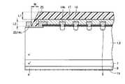
また、半導体基板1の第1主表面では、第1領域R1を取り囲むように、外周接合領域として第2領域R2が設けられている。その第2領域R2では、ガードリングとなるp層5が表面から所定の深さにわたり形成されている。第2領域R2には、p層5に接触するようにAlSi層14bが形成されている。そのAlSi層14bを覆うように、半絶縁性シリコン窒化膜17が形成されている。第2領域R2の外側の半導体基板1の第3領域の表面にはn層6が形成されている。そのn層6上には、最外周に位置するAlSi層14bから距離を隔てて、段差部20となるAlSi層14cが形成されている。Further, on the first main surface of the semiconductor substrate 1, a second region R2 is provided as an outer peripheral bonding region so as to surround the first region R1. In the second region R2, the
そして、本半導体装置では、分極による電界強度を緩和するための膜の一つとして、第2領域R2において、半絶縁性シリコン窒化膜17を覆うように、たとえば、ポリイミド膜などのオーバーコート膜18が形成されている。AiSi層14cは、オーバーコート膜18を塗布形成する際に、ポリイミドなどのオーバーコート材が外側へ向かって流れ出るのを阻止する機能を果たす。一方、半導体基板1の第2主表面側には、n+バッファ層7およびp+コレクタ層8が形成され、p+コレクタ層8の表面にはコレクタ電極15が形成されている。ダイシングされたチップ50は、所定の基板57に搭載されて、封止ゲル55によって封止されることになる(図10参照)。 In the present semiconductor device, as one of the films for relaxing the electric field strength due to polarization, an
上述した半導体装置では、半絶縁性シリコン窒化膜17を覆うように、オーバーコート膜18が形成されている。これにより、封止ゲル中に含まれる不純物イオンが分極することに起因して、コレクタ−エミッタ間電流(ICES)特性やコレクタ−エミッタ間電圧(VCES)特性等が不安定になるを防止することができる。このことについて、まず、オーバーコート膜が形成されていない半導体装置の場合について説明する。In the semiconductor device described above, the
図2に示すように、半導体装置の耐圧評価では、コレクタ電極15とエミッタ電極14aとの間に所定の電圧が印加される。この耐圧はオフ時の耐圧であって、半導体装置の定格電圧に対応した耐圧を保障する必要がある。たとえば、定格電圧が、6.5kV、4.5kV、3.3kVの半導体装置の場合には、コレクタ電極15とエミッタ電極14aとの間には、それぞれ6.5kV、4.5kV、3.3kVの電圧を印加することになる。 As shown in FIG. 2, in the breakdown voltage evaluation of the semiconductor device, a predetermined voltage is applied between the
このとき、コレクタ電極15とn層6が高電位側に接続され、エミッタ電極14a等は接地電位(GND)側に接続される。n層6は、ガードリングとなるp層5が形成された第2領域R2よりも外側の第3領域R3に位置し、エミッタ電極14a等は第2領域R2よりも内側の第1領域R1に位置する。 At this time, the
そのため、第2領域R2に形成された半絶縁性シリコン窒化膜17の表面上のうち、内側に位置する部分の表面上には封止ゲル中に含まれる不純物イオンのうちプラスイオン41が集まり、外側に位置する部分の表面上にはマイナスイオン42が集まる。こうして、不純物イオンの分極が発生することになる。最外周に位置するp層5の上方に集まったマイナスイオン42の影響によって、p層5の外側に位置するn-ドリフト層2の部分には、反転層としてp層13が形成されることになる。 Therefore, out of the surface of the semi-insulating
一方、コレクタ電極15とエミッタ電極14aとの間に所定の電圧が印加されることで、p層ベース層3とn-ドリフト層2との界面等から、主としてn-ドリフト層2の側へ空乏層31が伸びることになる。このとき、p層13が形成されることによって、空乏層はより外側へ向かって伸びやすくなる。そのため、外周部に位置するn層6の近傍(点線枠A)では、空乏層の伸びに歪が発生する。その結果、チップの外周部分において電界強度が強くなって、耐圧特性が低下することになる。 On the other hand, when a predetermined voltage is applied between the
これに対して、本半導体装置では、図3に示すように、ガードリングとしてのp層5が形成された第2領域では、半絶縁性シリコン窒化膜17を覆うようにオーバーコート膜18が形成されている。これにより、空乏層32は、マイナスイオン42とプラスイオン41との分極による影響を受けにくくなって、空乏層の伸びが安定する。その結果、設計値どおりの電界強度および耐圧特性を得ることができる。 On the other hand, in this semiconductor device, as shown in FIG. 3, an
しかも、本半導体装置では、第2領域R2の外側の第3領域R3に、段差部20としての所定の厚みのAlSi層14cが形成されている。これにより、塗布されたオーバーコート材が第3領域R3からさらに外側に位置するダイシングライン領域に向かって流れ出すのを阻止することができて、ダイシングライン領域にオーバーコート材が流れ出すことによってダイシングが良好に行われなくなることを防止することができる。 Moreover, in the present semiconductor device, an AlSi layer 14c having a predetermined thickness as the stepped
次に、上述した半導体装置の製造方法について説明する。図4に示すように、半導体基板1の第1主表面の第1領域に、IGBTとなるpベース層3、nソース層4、ゲート電極11が形成される。第1領域の外側に位置する第2領域にガードリングとなるp層5が形成され、第2領域の外側に位置する第3領域にn層6が形成される。次に、ゲート電極11上に層間絶縁膜12を介在させて、ゲート電極11を覆うようにAlSi層14が形成される。一方、半導体基板1の第2主表面には、n+バッファ層7、p+コレクタ層8およびコレクタ電極15が形成される。 Next, a method for manufacturing the semiconductor device described above will be described. As shown in FIG. 4,
次に、AlSi層14上に所定のレジストパターン(図示せず)が形成される。そのレジストパターンをマスクとして、AlSi層14に異方性エッチングを施すことにより、、図5に示すように、第1領域R1では、エミッタ電極14aが形成され、第2領域R2では、p層5に接続されるAlSi層14bが形成される。そして、第3領域R3では、段差部20としての所定の高さのAlSi層14cが形成される。その後、レジストパターンが除去される。 Next, a predetermined resist pattern (not shown) is formed on the
次に、図6に示すように、エミッタ電極14a等を覆うように、半導体基板の第1主表面上に半絶縁性シリコン窒化膜17が形成される。その半絶縁性シリコン窒化膜17上に、第2領域R2に位置する半絶縁性シリコン窒化膜17の部分を残す態様で、所定のレジストパターン(図示せず)が形成される。そのレジストパターンをマスクとして、半絶縁性シリコン窒化膜17に異方性エッチングを施すことにより、図7に示すように、第2領域R2に位置する半絶縁性シリコン窒化膜17の部分を残して、他の第1領域R1および第3領域R3に位置する半絶縁性シリコン窒化膜17の部分が除去される。その後、レジストパターンが除去される。 Next, as shown in FIG. 6, a semi-insulating
次に、図8に示すように、半導体基板の第1主表面における第2領域R2に、ディップ方式によって、たとえばポリイミドなどのオーバーコート材が塗布されて、半絶縁性シリコン窒化膜17を覆うようにオーバーコート膜18が形成される。このとき、所定の厚みのAlSi層14cが形成されていることで、塗布されたオーバーコート材が第3領域R3からさらに外側に位置するダイシングライン領域に向かって流れ出すのを阻止することができる。これにより、ダイシングライン領域にオーバーコート材が流れ出すことによってダイシングが良好に行われなくなるを防止することができる。そして、所望の厚さのオーバーコート膜18を第2領域R2に形成することができて、耐圧特性等が悪化するのを防止することができる。 Next, as shown in FIG. 8, an overcoat material such as polyimide is applied to the second region R2 on the first main surface of the semiconductor substrate by a dipping method so as to cover the semi-insulating
次に、図9に示すように、半導体基板1をダイシングライン領域においてダイシングすることにより、チップ50として取り出される。その後、図10に示すように、チップ50のコレクタ電極15が、はんだ53により、所定の基板51に設けられた基板電極52に接合される。基板51に接合されたチップ50は、封止ゲル55によって封止される。こうして、チップ50は、所定の基板51に搭載され封止ゲル55によって封止されて、パワーモジュールとして完成する。 Next, as shown in FIG. 9, the semiconductor substrate 1 is diced in a dicing line region, and is taken out as a
上述した半導体装置では、所定の厚みのAlSi層14cが形成されていることで、ポリイミドなどのオーバーコート材を塗布する際に、塗布されたオーバーコート材が第3領域R3からさらに外側に向かって流れ出すのを阻止することができる。これにより、所望の厚さのオーバーコート膜18を第2領域R2に形成することができて、耐圧特性等が悪化するのを防止することができる。 In the semiconductor device described above, since the AlSi layer 14c having a predetermined thickness is formed, when the overcoat material such as polyimide is applied, the applied overcoat material further moves outward from the third region R3. It can be prevented from flowing out. Thereby, the
また、上述した製造方法では、ダイシングする前にオーバーコート材を塗布する場合について説明したが、ダイシングを行った後にチップの状態で、オーバーコート材を塗布するようにしてもよい。この場合には、オーバーコート材を塗布する際に、オーバーコート材が流れ出して、オーバーコート材が半導体基板1の裏側のコレクタ電極15に回りこんでしまい、チップ50を所定の基板にはんだ付けができなくなくなるのを防止することができる。さらに、チップを基板にはんだ付けした後に、オーバーコート材を塗布する際に、流れ出したオーバーコート材が、チップ以外の他の部品に付着するのを防止して、組み立て不良を減らすことができる。 In the above-described manufacturing method, the case where the overcoat material is applied before dicing has been described. However, the overcoat material may be applied in a chip state after dicing. In this case, when the overcoat material is applied, the overcoat material flows out, and the overcoat material wraps around the
発明者は、種々の評価を行った結果、安定した耐圧特性を得るには、オーバーコート膜18の膜厚は30μm以上必要であることを見出した。このことについて説明する。図11に、コレクタ−エミッタ間電流(ICES)のオーバーコート膜の膜厚依存性のグラフを示す。パワーモジュールのIGBTでは、コレクタ−エミッタ間電流(ICES)は1A/cm2以下となることが好ましいとされる。そうすると、図11に示すグラフから、オーバーコート膜18の膜厚は30μm以上にする必要があることがわかる。As a result of various evaluations, the inventor has found that the film thickness of the
40μm以上の膜厚のオーバーコート膜を形成するには、一般的な半導体プロセスにおける写真製版では困難である。このことから、上述したように、ディスペンス方式による塗布が好ましい。また、ディスペンス方式の他に、印刷マスクを用いた印刷方式による塗布によっても所望の厚さのオーバーコート膜を形成することができる。さらに、本半導体装置では、ポリイミドなどのオーバーコート材が流れ出すのを阻止する段差部20が形成されていることで、オーバーコート材が流れ出すことによって、第2領域(外周接合領域)R2におけるオーバーコート膜が部分的に薄くなり、耐圧特性がばらつくのを抑制することができる。また、所望の厚さのオーバーコート膜を、必要最小限のオーバーコート材の量で形成することができる。 Forming an overcoat film having a thickness of 40 μm or more is difficult by photolithography in a general semiconductor process. For this reason, as described above, the dispensing method is preferable. In addition to the dispensing method, an overcoat film having a desired thickness can be formed by coating by a printing method using a printing mask. Further, in the present semiconductor device, the
また、図12に示すように、半絶縁性シリコン窒化膜17の上面上に位置するオーバーコート膜18の膜厚をL1、段差部20としてのAlSi層14cの高さをL2、最外周に位置するAlSi層の部分とAlSi層14cとの間に形成される溝25の幅をWとすると、オーバーコート材がチップの外側へ流れ出るのを阻止するには、次の関係式、
W≧(L1+L2)/2×(L1/L2)
を満たすことが好ましい。オーバーコート材が流れ出るのを阻止するには、オーバーコート膜の厚みが厚いほど、溝としてより広い幅Wが必要となる。また、高さL2が高いほど、より狭い幅Wでオーバーコート材が流れ出るのを阻止することができる。Further, as shown in FIG. 12, the thickness of the
W ≧ (L1 + L2) / 2 × (L1 / L2)
It is preferable to satisfy. In order to prevent the overcoat material from flowing out, the thicker the overcoat film, the wider the width W required for the groove. Further, the higher the height L2, the more the overcoat material can be prevented from flowing out with a narrower width W.
なお、上述した半導体装置では、半絶縁性シリコン窒化膜を覆うオーバコート膜の材料として、ポリイミドを例に挙げたが、ポリイミドの他に、たとえば、ポリアミドイミド等でもよく、誘電率が約3.5以下程度の比較的低い材料であれば、分極による影響を阻止することができる。 In the semiconductor device described above, polyimide is taken as an example of the material of the overcoat film covering the semi-insulating silicon nitride film. However, in addition to polyimide, for example, polyamideimide may be used, and the dielectric constant is about 3. If it is a relatively low material of about 5 or less, the influence of polarization can be prevented.
実施の形態2
ここでは、電力用の半導体素子としてIGBTを備えた電力用の半導体装置の他の例について説明する。図13に示すように、第2領域R2に位置するAlSi層14bを覆う半絶縁性シリコン窒化膜17aに加えて、第3領域R3に位置する段差部20としてのAlSi層14cの上面上に、半絶縁性シリコン窒化膜17bが形成されている。なお、これ以外の構成については図1に示す半導体装置と同様なので、同一部材には同一符号を付しその説明を省略する。
Here, another example of a power semiconductor device including an IGBT as a power semiconductor element will be described. As shown in FIG. 13, in addition to the semi-insulating
次に、上述した半導体装置の製造方法について説明する。前述した図4および図5に示す工程と同様の工程を経た後、図14に示すように、エミッタ電極14a等を覆うように、半導体基板1の第1主表面上に半絶縁性シリコン窒化膜17が形成される。次に、その半絶縁性シリコン窒化膜17の表面に、AlSi層14cの上に位置する半絶縁性シリコン窒化膜17の部分が残される態様で、所定のレジストパターン(図示せず)が形成される。 Next, a method for manufacturing the semiconductor device described above will be described. 4 and FIG. 5, the semi-insulating silicon nitride film is formed on the first main surface of the semiconductor substrate 1 so as to cover the
そのレジストパターンをマスクとして、半絶縁性シリコン窒化膜17に異方性エッチングを施すことにより、図15に示すように、第2領域R2に位置する半絶縁性シリコン窒化膜17aの部分と、第3領域R3のAlSi層14cの上面上に位置する半絶縁性シリコン窒化膜17bの部分を残して、他の第1領域R1等に位置する半絶縁性シリコン窒化膜17の部分が除去される。その後、レジストパターンが除去される。 Using the resist pattern as a mask, anisotropic etching is performed on the semi-insulating
次に、図16に示すように、半導体基板の第1主表面における第2領域R2に、ディップ方式によってポリイミドなどのオーバーコート材が塗布されて、半絶縁性シリコン窒化膜17aを覆うようにオーバーコート膜18が形成される。このとき、所定の厚みのAlSi層14cが形成されていることで、塗布されたポリイミドが第3領域R3からさらに外側に位置するダイシングライン領域に向かって流れ出すのを阻止することができる。Next, as shown in FIG. 16, the second region R2 of the first main surface of the semiconductor substrate, overcoat material such as polyimide is applied by dipping method, so as to cover the semi-insulating
次に、図17に示すように、半導体基板1をダイシングライン領域においてダイシングすることにより、チップ50として取り出される。その後、図10に示す工程と同様の工程を経て、チップは所定の基板に接合され、封止ゲルによって封止されて、パワーモジュールとして完成する(図示せず)。 Next, as shown in FIG. 17, the semiconductor substrate 1 is diced in a dicing line region to be taken out as a
上述した半導体装置では、前述した半導体装置と同様に、所定の厚みのAlSi層14cが形成されていることで、ポリイミドなどのオーバーコート材を塗布する際に、塗布されたオーバーコート材が第3領域R3からさらに外側に向かって流れ出すのを阻止することができる。すなわち、図18に示すように、半絶縁性シリコン窒化膜17の上面上に位置するオーバーコート膜18の膜厚をL1、AlSi層14cの高さをL2、最外周に位置するAlSi層の部分とAlSi層14cとの間に形成される溝の幅をWとすると、次の関係式、
W≧(L1+L2)/2×(L1/L2)
を満たすように設定されていることで、オーバーコート材がチップの外側へ流れ出るのを阻止して、所望の厚さのオーバーコート膜18を第2領域R2に形成することができ、耐圧特性等が悪化するのを防止することができる。In the semiconductor device described above, similarly to the semiconductor device described above, the AlSi layer 14c having a predetermined thickness is formed, so that when the overcoat material such as polyimide is applied, the applied overcoat material is the third. It is possible to prevent the flow from the region R3 further outward. That is, as shown in FIG. 18, the thickness of the
W ≧ (L1 + L2) / 2 × (L1 / L2)
By setting so as to satisfy, the overcoat material can be prevented from flowing out of the chip, and the
特に、本半導体装置では、段差部20としてのAlSi層14cの上面上に、さらに、半絶縁性シリコン窒化膜17bが形成されている。これにより、塗布されたオーバーコート材が第3領域R3から流れ出るのを確実に阻止することができる。 In particular, in this semiconductor device, a semi-insulating
なお、上述した各半導体装置では、電力用半導体素子としてIGBTを例に挙げて説明したが、IGBTの他に、たとえばダイオード等の素子でもよい。 In each of the semiconductor devices described above, the IGBT is described as an example of the power semiconductor element. However, in addition to the IGBT, an element such as a diode may be used.
今回開示された実施の形態は例示であってこれに制限されるものではない。本発明は上記で説明した範囲ではなく、特許請求の範囲によって示され、特許請求の範囲と均等の意味および範囲でのすべての変更が含まれることが意図される。 The embodiment disclosed this time is an example, and the present invention is not limited to this. The present invention is defined by the terms of the claims, rather than the scope described above, and is intended to include any modifications within the scope and meaning equivalent to the terms of the claims.
1 半導体基板、2 n-ドリフト層、3 pベース層、4 nソース層、5 p層、6 n層、7 n+バッファ層、8 p+コレクタ層、10 シリコン酸化膜、11 ゲート電極、12 層間絶縁膜、13 p反転層、14a エミッタ電極、15 コレクタ電極、14b AlSi膜、17 半絶縁性シリコン窒化膜、18 オーバーコート膜、20 段差部、14c AlSi膜、25 溝、31 空乏層、32 空乏層、41 プラスイオン、42 マイナスイオン、50 チップ、51 基板、52 電極、53 はんだ、55 封止ゲル、R1 第1領域、R2 第2領域、R3 第3領域。 DESCRIPTION OF SYMBOLS 1 Semiconductor substrate, 2 n-drift layer, 3 p base layer, 4 n source layer, 5 p layer, 6 n layer, 7 n + buffer layer, 8 p + collector layer, 10 Silicon oxide film, 11 Gate electrode, 12 Interlayer insulating film, 13 p inversion layer, 14a emitter electrode, 15 collector electrode, 14b AlSi film, 17 semi-insulating silicon nitride film, 18 overcoat film, 20 stepped portion, 14c AlSi film, 25 groove, 31 depletion layer, 32 Depletion layer, 41 positive ions, 42 negative ions, 50 chips, 51 substrate, 52 electrodes, 53 solder, 55 sealing gel, R1 first region, R2 second region, R3 third region.
Claims (4)
Translated fromJapanese前記半導体基板における前記第1主表面の第1領域に形成された第1電極および前記第2主表面に形成された第2電極を含み、前記第1電極と前記第2電極との間で電流が流される電力用半導体素子と、
前記第1領域よりも外側に位置する、前記第1主表面の第2領域に形成された第2導電型のガードリングと、
前記第2領域を覆うように形成された半絶縁性絶縁膜と、
前記半絶縁性絶縁膜の全体を覆うように、前記第2領域に形成された誘電体膜と、
前記第2領域よりも外側に位置する、前記第1主表面の第3領域に、前記半絶縁性絶縁膜とは距離を隔てられるとともに、前記半導体基板との間に前記誘電体膜の部分を介在させないように形成され、前記誘電体膜となる材料が流れ出るのを阻止する流動阻止部と
を備えた、半導体装置。A first conductivity type semiconductor substrate having opposing first main surface and second main surface;
A first electrode formed on a first region of the first main surface of the semiconductor substrate and a second electrode formed on the second main surface, wherein a current flows between the first electrode and the second electrode. A power semiconductor element through which current flows,
A second conductivity type guard ring formed in the second region of the first main surface, located outside the first region;
A semi-insulating insulating film formed to cover the second region;
A dielectric film formed in the second region so as to cover the entire semi-insulating insulating film;
The third region of the first main surface located outside the second region is spaced apart from the semi-insulating insulating film, andthe portion of the dielectric film is disposed between the semiconductor substrate and the third region.A semiconductor device comprising: a flow blocking portion that is formed soas not to intervene and blocks the material that becomes the dielectric film from flowing out.
Priority Applications (4)
| Application Number | Priority Date | Filing Date | Title |
|---|---|---|---|
| JP2008195062AJP5477681B2 (en) | 2008-07-29 | 2008-07-29 | Semiconductor device |
| US12/339,702US8450828B2 (en) | 2008-07-29 | 2008-12-19 | Semiconductor device |
| KR1020090019678AKR101055987B1 (en) | 2008-07-29 | 2009-03-09 | Semiconductor devices |
| DE102009014056.5ADE102009014056B4 (en) | 2008-07-29 | 2009-03-20 | Semiconductor device |
Applications Claiming Priority (1)
| Application Number | Priority Date | Filing Date | Title |
|---|---|---|---|
| JP2008195062AJP5477681B2 (en) | 2008-07-29 | 2008-07-29 | Semiconductor device |
Publications (3)
| Publication Number | Publication Date |
|---|---|
| JP2010034306A JP2010034306A (en) | 2010-02-12 |
| JP2010034306A5 JP2010034306A5 (en) | 2010-12-24 |
| JP5477681B2true JP5477681B2 (en) | 2014-04-23 |
Family
ID=41501446
Family Applications (1)
| Application Number | Title | Priority Date | Filing Date |
|---|---|---|---|
| JP2008195062AActiveJP5477681B2 (en) | 2008-07-29 | 2008-07-29 | Semiconductor device |
Country Status (4)
| Country | Link |
|---|---|
| US (1) | US8450828B2 (en) |
| JP (1) | JP5477681B2 (en) |
| KR (1) | KR101055987B1 (en) |
| DE (1) | DE102009014056B4 (en) |
Families Citing this family (41)
| Publication number | Priority date | Publication date | Assignee | Title |
|---|---|---|---|---|
| US9990674B1 (en) | 2007-12-14 | 2018-06-05 | Consumerinfo.Com, Inc. | Card registry systems and methods |
| US8312033B1 (en) | 2008-06-26 | 2012-11-13 | Experian Marketing Solutions, Inc. | Systems and methods for providing an integrated identifier |
| US8060424B2 (en) | 2008-11-05 | 2011-11-15 | Consumerinfo.Com, Inc. | On-line method and system for monitoring and reporting unused available credit |
| CN102217070B (en)* | 2009-09-03 | 2013-09-25 | 松下电器产业株式会社 | Semiconductor device and method for producing same |
| GB2496067B (en)* | 2010-06-17 | 2014-12-24 | Abb Technology Ag | Power semiconductor device |
| JP2012004466A (en)* | 2010-06-21 | 2012-01-05 | Hitachi Ltd | Semiconductor device |
| JP5708124B2 (en)* | 2011-03-25 | 2015-04-30 | 三菱電機株式会社 | Semiconductor device |
| US9483606B1 (en) | 2011-07-08 | 2016-11-01 | Consumerinfo.Com, Inc. | Lifescore |
| US9106691B1 (en) | 2011-09-16 | 2015-08-11 | Consumerinfo.Com, Inc. | Systems and methods of identity protection and management |
| US8738516B1 (en) | 2011-10-13 | 2014-05-27 | Consumerinfo.Com, Inc. | Debt services candidate locator |
| JP5600698B2 (en)* | 2012-03-14 | 2014-10-01 | 株式会社 日立パワーデバイス | Power semiconductor module with SiC element |
| US9853959B1 (en) | 2012-05-07 | 2017-12-26 | Consumerinfo.Com, Inc. | Storage and maintenance of personal data |
| US9654541B1 (en) | 2012-11-12 | 2017-05-16 | Consumerinfo.Com, Inc. | Aggregating user web browsing data |
| US9916621B1 (en) | 2012-11-30 | 2018-03-13 | Consumerinfo.Com, Inc. | Presentation of credit score factors |
| CN104995736B (en)* | 2013-02-15 | 2018-03-30 | 丰田自动车株式会社 | Semiconductor device and its manufacture method |
| US8836090B1 (en)* | 2013-03-01 | 2014-09-16 | Ixys Corporation | Fast recovery switching diode with carrier storage area |
| US10102570B1 (en) | 2013-03-14 | 2018-10-16 | Consumerinfo.Com, Inc. | Account vulnerability alerts |
| US9406085B1 (en) | 2013-03-14 | 2016-08-02 | Consumerinfo.Com, Inc. | System and methods for credit dispute processing, resolution, and reporting |
| US10685398B1 (en) | 2013-04-23 | 2020-06-16 | Consumerinfo.Com, Inc. | Presenting credit score information |
| CN104253151B (en) | 2013-06-27 | 2017-06-27 | 无锡华润上华半导体有限公司 | Field stop type reverse conducting insulated gate bipolar transistor and manufacturing method thereof |
| CN104332403A (en)* | 2013-07-22 | 2015-02-04 | 无锡华润上华半导体有限公司 | Semiconductor power device and manufacturing method thereof |
| US10325314B1 (en) | 2013-11-15 | 2019-06-18 | Consumerinfo.Com, Inc. | Payment reporting systems |
| US9477737B1 (en) | 2013-11-20 | 2016-10-25 | Consumerinfo.Com, Inc. | Systems and user interfaces for dynamic access of multiple remote databases and synchronization of data based on user rules |
| US9892457B1 (en) | 2014-04-16 | 2018-02-13 | Consumerinfo.Com, Inc. | Providing credit data in search results |
| DE102014005879B4 (en)* | 2014-04-16 | 2021-12-16 | Infineon Technologies Ag | Vertical semiconductor device |
| US10361266B2 (en)* | 2014-06-09 | 2019-07-23 | Panasonic Intellectual Property Management Co., Ltd. | Semiconductor device |
| CN107534061B (en)* | 2015-04-14 | 2020-09-22 | 三菱电机株式会社 | Semiconductor device with a plurality of transistors |
| JP6627359B2 (en)* | 2015-09-17 | 2020-01-08 | 富士電機株式会社 | Semiconductor device and method of manufacturing semiconductor device |
| JP6575398B2 (en)* | 2016-03-01 | 2019-09-18 | 三菱電機株式会社 | Semiconductor device |
| JP6834156B2 (en) | 2016-03-16 | 2021-02-24 | 富士電機株式会社 | Semiconductor devices and manufacturing methods |
| CN109155293B (en)* | 2016-05-17 | 2021-10-26 | 三菱电机株式会社 | Semiconductor device and method for manufacturing the same |
| WO2018131144A1 (en)* | 2017-01-13 | 2018-07-19 | 三菱電機株式会社 | Semiconductor device and method for manufacturing same |
| US10332817B1 (en)* | 2017-12-01 | 2019-06-25 | Cree, Inc. | Semiconductor die with improved ruggedness |
| DE102019100130B4 (en) | 2018-04-10 | 2021-11-04 | Infineon Technologies Ag | A SEMICONDUCTOR COMPONENT AND A METHOD OF FORMING A SEMICONDUCTOR COMPONENT |
| US11265324B2 (en) | 2018-09-05 | 2022-03-01 | Consumerinfo.Com, Inc. | User permissions for access to secure data at third-party |
| US11315179B1 (en) | 2018-11-16 | 2022-04-26 | Consumerinfo.Com, Inc. | Methods and apparatuses for customized card recommendations |
| US11238656B1 (en) | 2019-02-22 | 2022-02-01 | Consumerinfo.Com, Inc. | System and method for an augmented reality experience via an artificial intelligence bot |
| US11941065B1 (en) | 2019-09-13 | 2024-03-26 | Experian Information Solutions, Inc. | Single identifier platform for storing entity data |
| US11600724B2 (en) | 2020-09-24 | 2023-03-07 | Wolfspeed, Inc. | Edge termination structures for semiconductor devices |
| JP2021007182A (en)* | 2020-10-19 | 2021-01-21 | 三菱電機株式会社 | Semiconductor devices and their manufacturing methods |
| JP7541898B2 (en) | 2020-11-04 | 2024-08-29 | ルネサスエレクトロニクス株式会社 | Semiconductor Device |
Family Cites Families (24)
| Publication number | Priority date | Publication date | Assignee | Title |
|---|---|---|---|---|
| JPS51128269A (en)* | 1975-04-30 | 1976-11-09 | Sony Corp | Semiconductor unit |
| GB2131603B (en) | 1982-12-03 | 1985-12-18 | Philips Electronic Associated | Semiconductor devices |
| JPS5936932A (en) | 1983-05-25 | 1984-02-29 | Hitachi Ltd | Semiconductor integrated circuit |
| JPS60102770A (en)* | 1983-11-09 | 1985-06-06 | Toshiba Corp | semiconductor equipment |
| EP0400178B1 (en)* | 1989-05-31 | 1994-08-03 | Siemens Aktiengesellschaft | Semiconductor device with a passivation layer |
| JP2975614B2 (en) | 1989-09-29 | 1999-11-10 | 富士電機株式会社 | Planar type semiconductor device |
| JP2870553B2 (en) | 1990-11-08 | 1999-03-17 | 富士電機株式会社 | High voltage semiconductor device |
| US5374843A (en)* | 1991-05-06 | 1994-12-20 | Silinconix, Inc. | Lightly-doped drain MOSFET with improved breakdown characteristics |
| JP3116976B2 (en) | 1992-05-08 | 2000-12-11 | 宇部興産株式会社 | Polyimide separation membrane |
| JP2812093B2 (en) | 1992-09-17 | 1998-10-15 | 株式会社日立製作所 | Semiconductor device having planar junction |
| JP3275536B2 (en)* | 1994-05-31 | 2002-04-15 | 三菱電機株式会社 | Semiconductor device and manufacturing method thereof |
| JPH09283754A (en)* | 1996-04-16 | 1997-10-31 | Toshiba Corp | High voltage semiconductor device |
| US5677562A (en)* | 1996-05-14 | 1997-10-14 | General Instrument Corporation Of Delaware | Planar P-N junction semiconductor structure with multilayer passivation |
| JP2002522904A (en)* | 1998-08-05 | 2002-07-23 | インフィネオン テクノロジース アクチエンゲゼルシャフト | Substrate for high voltage module |
| JP3545633B2 (en)* | 1999-03-11 | 2004-07-21 | 株式会社東芝 | High breakdown voltage semiconductor device and method of manufacturing the same |
| NL1018793C2 (en) | 2001-06-11 | 2002-12-12 | Sjoerd Meijer | Forklift truck with loading system. |
| TW583748B (en)* | 2003-03-28 | 2004-04-11 | Mosel Vitelic Inc | The termination structure of DMOS device |
| JP2004349383A (en)* | 2003-05-21 | 2004-12-09 | Toshiba Corp | High voltage semiconductor device |
| GB0407363D0 (en)* | 2004-03-31 | 2004-05-05 | Koninkl Philips Electronics Nv | Trench semiconductor device and method of manufacturing it |
| US7820473B2 (en)* | 2005-03-21 | 2010-10-26 | Semiconductor Components Industries, Llc | Schottky diode and method of manufacture |
| EP1722423B1 (en)* | 2005-05-12 | 2016-07-06 | Ixys Corporation | Stable diodes for low and high frequency applications |
| JP5050329B2 (en)* | 2005-08-26 | 2012-10-17 | サンケン電気株式会社 | Trench structure semiconductor device and manufacturing method thereof |
| JP2007201247A (en)* | 2006-01-27 | 2007-08-09 | Mitsubishi Electric Corp | High voltage semiconductor device |
| DE102006013077A1 (en)* | 2006-03-22 | 2007-09-27 | Semikron Elektronik Gmbh & Co. Kg | Power semiconductor component with secondary passivation layer and associated manufacturing method |
- 2008
- 2008-07-29JPJP2008195062Apatent/JP5477681B2/enactiveActive
- 2008-12-19USUS12/339,702patent/US8450828B2/enactiveActive
- 2009
- 2009-03-09KRKR1020090019678Apatent/KR101055987B1/ennot_activeExpired - Fee Related
- 2009-03-20DEDE102009014056.5Apatent/DE102009014056B4/enactiveActive
Also Published As
| Publication number | Publication date |
|---|---|
| KR101055987B1 (en) | 2011-08-11 |
| KR20100012792A (en) | 2010-02-08 |
| JP2010034306A (en) | 2010-02-12 |
| US8450828B2 (en) | 2013-05-28 |
| DE102009014056B4 (en) | 2014-02-06 |
| US20100025820A1 (en) | 2010-02-04 |
| DE102009014056A1 (en) | 2010-02-11 |
Similar Documents
| Publication | Publication Date | Title |
|---|---|---|
| JP5477681B2 (en) | Semiconductor device | |
| JP5517688B2 (en) | Semiconductor device | |
| US20200335490A1 (en) | Semiconductor device and method of manufacturing semiconductor device | |
| JP4797225B2 (en) | Semiconductor device | |
| CN104282686B (en) | Wide band gap semiconductor device | |
| JP5943819B2 (en) | Semiconductor element, semiconductor device | |
| US9627383B2 (en) | Semiconductor device | |
| US8564059B2 (en) | High-voltage vertical power component | |
| US10749026B2 (en) | Semiconductor device and method of manufacturing the semiconductor device | |
| US11177360B2 (en) | Semiconductor device | |
| JP2017098440A (en) | Semiconductor device | |
| US10256232B2 (en) | Semiconductor device including a switching element and a sense diode | |
| JP2017045827A (en) | Semiconductor device | |
| JP2014067986A (en) | Semiconductor device | |
| JP6422906B2 (en) | Semiconductor device | |
| US8686515B2 (en) | Double-groove bidirectional vertical component | |
| JP2008103530A (en) | Semiconductor device | |
| JP2016207829A (en) | Insulated gate type switching element | |
| JP2005026434A (en) | Semiconductor device | |
| JP6301551B1 (en) | Semiconductor device | |
| CN107710408B (en) | semiconductor device | |
| CN112103288A (en) | Semiconductor device and method for manufacturing semiconductor device | |
| JP5092202B2 (en) | Semiconductor device | |
| JP7404601B2 (en) | semiconductor integrated circuit | |
| JP7224247B2 (en) | semiconductor equipment |
Legal Events
| Date | Code | Title | Description |
|---|---|---|---|
| A521 | Request for written amendment filed | Free format text:JAPANESE INTERMEDIATE CODE: A523 Effective date:20101105 | |
| A621 | Written request for application examination | Free format text:JAPANESE INTERMEDIATE CODE: A621 Effective date:20101105 | |
| A977 | Report on retrieval | Free format text:JAPANESE INTERMEDIATE CODE: A971007 Effective date:20130117 | |
| A131 | Notification of reasons for refusal | Free format text:JAPANESE INTERMEDIATE CODE: A131 Effective date:20130122 | |
| A521 | Request for written amendment filed | Free format text:JAPANESE INTERMEDIATE CODE: A523 Effective date:20130321 | |
| A131 | Notification of reasons for refusal | Free format text:JAPANESE INTERMEDIATE CODE: A131 Effective date:20130716 | |
| A521 | Request for written amendment filed | Free format text:JAPANESE INTERMEDIATE CODE: A523 Effective date:20130912 | |
| TRDD | Decision of grant or rejection written | ||
| A01 | Written decision to grant a patent or to grant a registration (utility model) | Free format text:JAPANESE INTERMEDIATE CODE: A01 Effective date:20140114 | |
| A61 | First payment of annual fees (during grant procedure) | Free format text:JAPANESE INTERMEDIATE CODE: A61 Effective date:20140130 | |
| R150 | Certificate of patent or registration of utility model | Ref document number:5477681 Country of ref document:JP Free format text:JAPANESE INTERMEDIATE CODE: R150 | |
| R250 | Receipt of annual fees | Free format text:JAPANESE INTERMEDIATE CODE: R250 | |
| R250 | Receipt of annual fees | Free format text:JAPANESE INTERMEDIATE CODE: R250 | |
| R250 | Receipt of annual fees | Free format text:JAPANESE INTERMEDIATE CODE: R250 | |
| R250 | Receipt of annual fees | Free format text:JAPANESE INTERMEDIATE CODE: R250 | |
| R250 | Receipt of annual fees | Free format text:JAPANESE INTERMEDIATE CODE: R250 | |
| R250 | Receipt of annual fees | Free format text:JAPANESE INTERMEDIATE CODE: R250 | |
| R250 | Receipt of annual fees | Free format text:JAPANESE INTERMEDIATE CODE: R250 | |
| R250 | Receipt of annual fees | Free format text:JAPANESE INTERMEDIATE CODE: R250 | |
| R250 | Receipt of annual fees | Free format text:JAPANESE INTERMEDIATE CODE: R250 |