JP5477377B2 - Slot antenna, electronic device, and method for manufacturing slot antenna - Google Patents
Slot antenna, electronic device, and method for manufacturing slot antennaDownload PDFInfo
- Publication number
- JP5477377B2 JP5477377B2JP2011508194AJP2011508194AJP5477377B2JP 5477377 B2JP5477377 B2JP 5477377B2JP 2011508194 AJP2011508194 AJP 2011508194AJP 2011508194 AJP2011508194 AJP 2011508194AJP 5477377 B2JP5477377 B2JP 5477377B2
- Authority
- JP
- Japan
- Prior art keywords
- conductor plate
- slot
- slot antenna
- notch
- antenna
- Prior art date
- Legal status (The legal status is an assumption and is not a legal conclusion. Google has not performed a legal analysis and makes no representation as to the accuracy of the status listed.)
- Active
Links
- 238000000034methodMethods0.000titledescription11
- 238000004519manufacturing processMethods0.000titledescription5
- 239000004020conductorSubstances0.000claimsdescription99
- 238000012545processingMethods0.000claimsdescription2
- 239000002184metalSubstances0.000description72
- 229910052751metalInorganic materials0.000description72
- 238000010586diagramMethods0.000description19
- 230000005684electric fieldEffects0.000description9
- 239000011347resinSubstances0.000description7
- 229920005989resinPolymers0.000description7
- 230000009471actionEffects0.000description4
- 230000008901benefitEffects0.000description3
- 238000013461designMethods0.000description3
- 230000005855radiationEffects0.000description3
- 239000003990capacitorSubstances0.000description2
- 238000004891communicationMethods0.000description2
- 230000001681protective effectEffects0.000description2
- 238000005452bendingMethods0.000description1
- 230000008859changeEffects0.000description1
- 230000008878couplingEffects0.000description1
- 238000010168coupling processMethods0.000description1
- 238000005859coupling reactionMethods0.000description1
- 239000013013elastic materialSubstances0.000description1
- 230000001771impaired effectEffects0.000description1
- 238000010348incorporationMethods0.000description1
- 239000004973liquid crystal related substanceSubstances0.000description1
- 150000002739metalsChemical class0.000description1
- 230000003071parasitic effectEffects0.000description1
- 230000002093peripheral effectEffects0.000description1
- 230000009467reductionEffects0.000description1
- 239000000758substrateSubstances0.000description1
Images


Classifications
- H—ELECTRICITY
- H01—ELECTRIC ELEMENTS
- H01Q—ANTENNAS, i.e. RADIO AERIALS
- H01Q13/00—Waveguide horns or mouths; Slot antennas; Leaky-waveguide antennas; Equivalent structures causing radiation along the transmission path of a guided wave
- H01Q13/10—Resonant slot antennas
- H—ELECTRICITY
- H01—ELECTRIC ELEMENTS
- H01Q—ANTENNAS, i.e. RADIO AERIALS
- H01Q1/00—Details of, or arrangements associated with, antennas
- H01Q1/12—Supports; Mounting means
- H01Q1/22—Supports; Mounting means by structural association with other equipment or articles
- H01Q1/2258—Supports; Mounting means by structural association with other equipment or articles used with computer equipment
- H01Q1/2266—Supports; Mounting means by structural association with other equipment or articles used with computer equipment disposed inside the computer
- H—ELECTRICITY
- H01—ELECTRIC ELEMENTS
- H01Q—ANTENNAS, i.e. RADIO AERIALS
- H01Q1/00—Details of, or arrangements associated with, antennas
- H01Q1/12—Supports; Mounting means
- H01Q1/22—Supports; Mounting means by structural association with other equipment or articles
- H01Q1/24—Supports; Mounting means by structural association with other equipment or articles with receiving set
- H01Q1/241—Supports; Mounting means by structural association with other equipment or articles with receiving set used in mobile communications, e.g. GSM
- H01Q1/242—Supports; Mounting means by structural association with other equipment or articles with receiving set used in mobile communications, e.g. GSM specially adapted for hand-held use
- H01Q1/243—Supports; Mounting means by structural association with other equipment or articles with receiving set used in mobile communications, e.g. GSM specially adapted for hand-held use with built-in antennas
- Y—GENERAL TAGGING OF NEW TECHNOLOGICAL DEVELOPMENTS; GENERAL TAGGING OF CROSS-SECTIONAL TECHNOLOGIES SPANNING OVER SEVERAL SECTIONS OF THE IPC; TECHNICAL SUBJECTS COVERED BY FORMER USPC CROSS-REFERENCE ART COLLECTIONS [XRACs] AND DIGESTS
- Y10—TECHNICAL SUBJECTS COVERED BY FORMER USPC
- Y10T—TECHNICAL SUBJECTS COVERED BY FORMER US CLASSIFICATION
- Y10T29/00—Metal working
- Y10T29/49—Method of mechanical manufacture
- Y10T29/49002—Electrical device making
- Y10T29/49016—Antenna or wave energy "plumbing" making
- Y10T29/49018—Antenna or wave energy "plumbing" making with other electrical component
Landscapes
- Engineering & Computer Science (AREA)
- Computer Hardware Design (AREA)
- General Engineering & Computer Science (AREA)
- Computer Networks & Wireless Communication (AREA)
- Waveguide Aerials (AREA)
- Support Of Aerials (AREA)
- Details Of Aerials (AREA)
Description
Translated fromJapanese本発明はスロットアンテナ及び電子機器に関し、特に複共振特性を有するスロットアンテナ、そのスロットアンテナを含む電子機器及びそのスロットアンテナの製造方法に関する。 The present invention relates to a slot antenna and an electronic device, and more particularly to a slot antenna having multiple resonance characteristics, an electronic device including the slot antenna, and a method of manufacturing the slot antenna.
近年、携帯無線端末の小型・薄型化に伴い、端末の剛性を確保するために金属製の筐体を用いた技術が幾つか公開されている。 In recent years, with the miniaturization and thinning of portable wireless terminals, several techniques using a metal casing have been disclosed in order to ensure the rigidity of the terminal.
また、近年の携帯無線端末は小型・薄型化と並行して、搭載される無線機能の増大、高機能化が進んでいる。このため、小型薄型の金属筐体に複数のアンテナを搭載する必要性が出てきているが、アンテナ実装スペースの制約からアンテナと金属の距離が非常に近くなる。一般にアンテナの近くに金属が配置されるとアンテナ特性が大きく劣化し、無線端末としての機能を満たさなくなるという問題がある。 In recent years, portable wireless terminals have been equipped with more wireless functions and higher functions in parallel with the reduction in size and thickness. For this reason, there is a need to mount a plurality of antennas on a small and thin metal casing, but the distance between the antenna and the metal becomes very short due to restrictions on the antenna mounting space. In general, when a metal is arranged near an antenna, there is a problem that the antenna characteristics are greatly deteriorated and the function as a wireless terminal is not satisfied.
このような問題に対して、金属が近くにあってもアンテナを動作させる技術として、金属筐体に細長い切れ込み(スロット)を設けて、これをアンテナとして動作させる技術が公示されている。一般的にスロットアンテナは狭帯域な特性であるので、複数のスロットを用いて複共振化させることで広帯域化を図る技術が周知となっている。 In order to deal with such a problem, as a technique for operating an antenna even when a metal is in the vicinity, a technique for providing an elongated cut (slot) in a metal casing and operating the antenna as an antenna has been publicly announced. In general, since slot antennas have a narrow band characteristic, a technique for widening a band by using a plurality of slots to achieve multiple resonance is well known.
特許文献1では、複数のスロットを形成し、複共振特性を実現したアンテナ装置が開示されている。この特許文献1のアンテナは、基板の縁端からの切れ込みにより構成されたノッチアンテナと、ノッチアンテナと平行に切り込まれた若干短めの無給電ノッチアンテナとで構成される。 Patent Document 1 discloses an antenna device in which a plurality of slots are formed to realize multi-resonance characteristics. The antenna of Patent Document 1 includes a notch antenna formed by cutting from an edge of a substrate, and a slightly shorter parasitic notch antenna cut in parallel with the notch antenna.
特許文献2には、2枚の導体板が対向して設けられ、各々の導体板はその1辺において他の導体板を介して接続されている。この2枚の導体板の一方には、他の導体板と接続する1辺に対向する1辺に開放端を有する隙間部(スリット)が形成されている。コンデンサC1、C2は隙間部を挟む位置に配置され、2枚の導体板間に接続されている。この特許文献2のアンテナは、隙間部が形成された導体板の隙間部の両サイドの領域により2つの共振を実現しており、コンデンサC1、C2によって調整している。 In Patent Document 2, two conductive plates are provided to face each other, and each conductive plate is connected on one side via another conductive plate. One of the two conductor plates is formed with a gap (slit) having an open end on one side opposite to one side connected to the other conductor plate. Capacitors C1 and C2 are arranged at positions sandwiching the gap, and are connected between two conductor plates. In the antenna of Patent Document 2, two resonances are realized by regions on both sides of the gap portion of the conductor plate in which the gap portion is formed, and the resonance is adjusted by capacitors C1 and C2.
しかし、特許文献1の技術では、複数のスロットを配置することでアンテナの実装スペースが大きくなるという問題がある。また、特許文献1のアンテナ構成は一方のスロットを電磁結合により動作させる構成である。この構成は2つのスロット間の距離によってアンテナ特性が大きく変化するため、特性の調整が難しいという問題がある。さらに、特許文献2のアンテナ構成はマイクロストリップアンテナ構成であり、文献内に記載されているスリットはアンテナとしては動作しない構成である。そのため、本構成をアンテナとして動作させるためにはアンテナ素子を形成している導体板の周囲にある程度の空間が必要となる。このためアンテナの実装スペースが大きくなるという問題と、文献2のアンテナを金属筐体に適用するのは困難という問題がある。 However, the technique of Patent Document 1 has a problem that an antenna mounting space is increased by arranging a plurality of slots. The antenna configuration of Patent Document 1 is a configuration in which one slot is operated by electromagnetic coupling. This configuration has a problem that it is difficult to adjust the characteristics because the antenna characteristics vary greatly depending on the distance between the two slots. Furthermore, the antenna configuration of Patent Document 2 is a microstrip antenna configuration, and the slit described in the document does not operate as an antenna. Therefore, in order to operate this configuration as an antenna, a certain amount of space is required around the conductor plate forming the antenna element. For this reason, there are a problem that the mounting space of the antenna becomes large and a problem that it is difficult to apply the antenna of Document 2 to a metal casing.
そこで、本発明はこのような問題点を解決するためになされたものであり、少ない実装スペースで複共振を得るスロットアンテナ、電子機器及びスロットアンテナ製造方法を提供することを目的とする。 Accordingly, the present invention has been made to solve such problems, and an object of the present invention is to provide a slot antenna, an electronic device, and a slot antenna manufacturing method that can obtain multiple resonances in a small mounting space.
本発明の第1の態様にかかるスロットアンテナは、開放端を有する切れ込みを導体板の1辺に設けた長方形の第1の導体板と、前記第1の導体板に対向して配置される長方形の第2の導体板と、前記第1の導体板と前記第2の導体板を前記開放端の反対側の辺で接続する第3の導体板と、
前記切れ込みを跨いだ2点で芯線とグランドが接続される給電線とを備えるものである。A slot antenna according to a first aspect of the present invention includes a rectangular first conductor plate provided with a notch having an open end on one side of a conductor plate, and a rectangle disposed opposite to the first conductor plate. A second conductive plate, a third conductive plate connecting the first conductive plate and the second conductive plate at a side opposite to the open end,
The power supply line is provided with a core wire and a ground connected at two points across the cut.
本発明の第2の態様にかかる電子機器は、実施の態様1に記載のスロットアンテナと、前記スロットアンテナを含む筺体とを備えるものである。 An electronic apparatus according to a second aspect of the present invention includes the slot antenna according to the first embodiment and a housing including the slot antenna.
本発明の第3の態様にかかるスロットアンテナ製造方法は、導体板の1辺に開放端を有する切れ込みを形成するステップと、前記導体板を加工し、前記切れ込みを跨いだ2点で芯線とグランドを接続した給電線を設けた第1の導体板と、前記第1の導体板に対向して配置される第2の導体板と、前記第1の導体板と前記第2の導体板を接続する第3の導体板を備えるスロットアンテナを形成するステップと、を備えることである。 According to a third aspect of the present invention, there is provided a slot antenna manufacturing method comprising: forming a notch having an open end on one side of a conductor plate; and processing the conductor plate and straddling the notch with a core wire and a ground at two points. A first conductor plate provided with a power supply line connected to the first conductor plate, a second conductor plate disposed opposite to the first conductor plate, and the first conductor plate and the second conductor plate connected to each other. Forming a slot antenna comprising a third conductor plate.
本発明により、少ない実装スペースで複共振を得るスロットアンテナ、電子機器及びスロットアンテナ製造方法を提供することができる。 According to the present invention, it is possible to provide a slot antenna, an electronic device, and a method for manufacturing a slot antenna that can obtain multiple resonances in a small mounting space.
(実施の形態1)
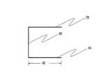
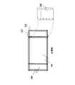
以下、図面を参照して本発明の実施の形態について説明する。図1は本発明の実施の形態1にかかるスロットアンテナの構造を示す図である。また、図2は本発明の実施の形態1にかかるスロットアンテナを図1のA方向から見た図である。本発明の実施の形態1のスロットアンテナは、導体板10乃至30と、給電線40とを備えている。(Embodiment 1)
Embodiments of the present invention will be described below with reference to the drawings. FIG. 1 is a diagram showing the structure of the slot antenna according to the first embodiment of the present invention. FIG. 2 is a diagram of the slot antenna according to the first exemplary embodiment of the present invention viewed from the direction A in FIG. The slot antenna according to the first embodiment of the present invention includes
導体板10は、給電線40が設けられ、かつ開放端を有する細長い切れ込み(以下、「スロット」と記載する)を1辺に設けている。ここでスロットの幅はスロットの長さd1と比較して充分小さいものとする。また、スロットと同一方向の導体板10の1辺の長さをd2とする。 The
導体板20は、導体板10に対向して配置されている。ここで、導体板10と導体板20との大きさは任意の大きさを有するものであり、本発明の実施の形態1では、導体板10と導体板20とは同一の大きさを有するものとして説明する。 The
導体板30は、スロットの開放端を設けた辺と反対側の辺において、導体板10と導体板20とを接続するように配置されている。 The
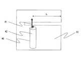
次に、給電線40の接続構成について図3を用いて説明する。給電線40は特性インピーダンス50Ωの同軸ケーブルで構成されるものであって、その芯線41と外皮のグランド導体42でスロットを跨ぐ様に2箇所で半田付け接続されている。半田付け接続する位置を給電位置としてスロットの開放端からの距離Lで示した場合、給電位置Lは、Z0×cos2(2πL/λg)=50を満たす位置が望ましい。本式を満たすことにより、アンテナと無線回路(図示せず)の間でインピーダンス整合をとることができる。ここでZ0≒487(Ω)であり、λgは、d1を1/4波長とする周波数の1波長に相当する電気長である。Next, the connection configuration of the
次に本実施の形態1にかかるスロットアンテナの動作について説明する。給電線40から電力を供給するスロットの周囲に電流が励起され、スロットの開放端側で電界が最大となり、スロットの短絡端側で電界が最小となるような定在波が生じる。その共振周波数は、スロット長d1を1/4波長とした周波数となる。また、これとは別の共振として、導体板10、20、30で構成されたコの字型のキャビティ構造に沿って電流が励起され、コの字型構造の開放端側で電界が最大となり、導体板30の配置した側で電界が最小となるような定在波が生じる。その共振周波数は導体板10においてスロット開放端のある辺から導体板30までの距離d2を1/4波長とした周波数となる。 Next, the operation of the slot antenna according to the first embodiment will be described. Current is excited around the slot for supplying power from the
スロットに起因した共振は、スロット幅方向に電界成分を有する共振モードであるのに対して、キャビティ構造に起因した共振は、対向した導体板10と20との間で両者の間隔方向に電界成分を有する共振モードである。2つの共振モードの電界成分は互いに直交するため、両者は干渉しないモードであることから、それぞれの共振周波数を個別に調整でき、調整作業を短時間で終了できるという利点がある。 The resonance caused by the slot is a resonance mode having an electric field component in the slot width direction, whereas the resonance caused by the cavity structure is an electric field component between the
ここで、導体板10乃至30の配置について具体的に説明する。導体板10と導体板20とは実質的に平行の位置に配置されてもよい。実質的にとしたのは、実際にアンテナを形成する場合において、厳密に平行状態を要求するものではない。また、上記説明では、導体板10と20とは同じサイズであるとしたが、これに限らず、導体板10が導体板20より大きなサイズであっても良い。また、スロットアンテナの開放端のある辺と導体板20の辺の位置関係は、スロット開放端のある辺が導体板20の辺と同じかあるいは外側にあることが望ましい。 Here, the arrangement of the
また、図1において導体板30は板状の構成であるとしたが、これに限らず、例えばガスケットのような弾性のある導電性の素材を用いて、導体板10と20を電気的に導通させる構造であっても良い。また、細長い棒状の金属を複数個所で離散的に配置して導体板10と20を接続する構成であっても良い。そのときの接続間隔は共振周波数に相当する波長の1/10以下であることが望ましい。また、導体板10と20の接続については、細長い棒状の金属を両者に対して半田付け接続しても良く、あるいは板バネのような弾性のある素材を用いて両者を押し当てることで電気的に導通させる構造でもよい。また、導体板30は少なくとも導体板10または20の長辺部分の上端からスロットの配置された位置まで配置され、導体板10と20を電気的に導通させることが好ましい。 In FIG. 1, the
また、図1においては、導体板30は長方形の導体板10及び導体板20の長辺と接続されているが、そこに限らず導体板10及び導体板20の内側に入った面部分で接続されてもよい。 In FIG. 1, the
さらに、図4に示すように導体板30は、L字型の形状を有し、導体板10及び20の長辺及び短辺と接続するように配置されてもよい。 Furthermore, as shown in FIG. 4, the
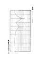
ここで、図5を用いて、本発明の実施の形態1にかかるスロットアンテナの入力インピーダンス特性を示す。縦軸はアンテナからの反射電力量を示し、横軸は周波数を示す。ここで図中の特性曲線において、谷の一番深い部分をアンテナの共振周波数とする。図1のアンテナ構成ではスロットの長さd1とキャビティ構造のd2の関係はd1<d2であるので、低周波数側の共振周波数f2はキャビティ構造のd2で決まる。一方、高周波数側の共振周波数f1は、スロットの長さd1で決まる。 Here, FIG. 5 is used to show the input impedance characteristics of the slot antenna according to the first exemplary embodiment of the present invention. The vertical axis represents the amount of reflected power from the antenna, and the horizontal axis represents the frequency. Here, in the characteristic curve in the figure, the deepest part of the valley is the resonance frequency of the antenna. In the antenna configuration of FIG. 1, since the relationship between the slot length d1 and the cavity structure d2 is d1 <d2, the resonance frequency f2 on the low frequency side is determined by the cavity structure d2. On the other hand, the resonance frequency f1 on the high frequency side is determined by the slot length d1.
以上説明したように、本発明の実施の形態1にかかるスロットアンテナを用いることにより、スロット部分の作用による共振と、導体板10乃至30で形成されたキャビティ構造の作用による共振が得られ、複共振化が実現できる。また、本アンテナ構成はキャビティ構造にスロットを1つのみ設けたシンプルな構成であるので、少ない実装スペースにて複共振アンテナを実現することができる。また、本アンテナ構成で得られる2つの共振モードは互いに干渉しないモードであるため、それぞれの共振周波数の調整が容易に行えるという利点がある。 As described above, by using the slot antenna according to the first embodiment of the present invention, resonance due to the action of the slot portion and resonance due to the action of the cavity structure formed of the
また、導体板30をL字型の形状にし、導体板10及び20の長辺及び短辺と接続するように配置することで、アンテナと各種回路の間の電磁的な干渉を低減するシールド壁として作用し、アンテナ動作、周辺のデバイス及び各種回路の良好な動作を確保できる。 Moreover, the shield plate which reduces the electromagnetic interference between an antenna and various circuits by making the
(実施の形態2)
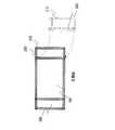
次に、図6を用いて、本発明の実施の形態2にかかるスロットアンテナの構造について説明する。なお、給電線40は図1と同様であるため、省略する。本発明の実施の形態2にかかるスロットアンテナは、スロットを90度に折り曲げることにより、スロットをL字の形状にすることを特徴としており、これ以外は実施の形態1の構成と同様である。開放端から導体板30方向の切れ込みの距離をd3とし、導体板30に平行に位置する切れ込みの距離をd4とする。この場合、d3+d4の距離を1/4波長とする周波数で共振が生じる。また、これとは別の共振として、導体板10、20、30で構成されたコの字型のキャビティ構造に沿って電流が励起され、コの字型構造の開放端側で電界が最大となり、導体板30の配置した側で電界が最小となるような定在波が生じる。その共振周波数は導体板10においてスロット開放端のある辺から導体板30までの距離d2を1/4波長とした周波数となる。(Embodiment 2)
Next, the structure of the slot antenna according to the second exemplary embodiment of the present invention will be described with reference to FIG. The
以上説明したように、本発明の実施の形態2にかかるスロットアンテナを用いると、スロット部分の作用による共振と、導体板10乃至30で形成されたキャビティ構造の作用による共振が得られ、複共振化が実現できる。またこの2つの共振のうち、スロットに起因した共振については、スロットの距離を長くとることができるので、より低い周波数の共振が得られる。 As described above, when the slot antenna according to the second embodiment of the present invention is used, resonance due to the action of the slot portion and resonance due to the action of the cavity structure formed by the
(実施の形態3)
次に、図7を用いて本発明の実施の形態3にかかるスロットアンテナの構造について説明する。なお、給電線40は図1と同様であるため、省略する。本発明の実施の形態3にかかるスロットアンテナは、導体板10の1辺であり、前記第3の導体板と接続されている一辺と前記開放端を有する一辺以外の一辺であって前記切れ込みに近い側の辺に、開放端を有するスロットを設けることを特徴としている。新たに設けられたスロットにより、d2の長さを調整する。つまり、距離d2に、切れ込みの長さd5を考慮することにより、距離d2は、d2+2×d5となる。これにより、d2+2×d5の距離を1/4波長とする周波数で共振する。(Embodiment 3)
Next, the structure of the slot antenna according to the third embodiment of the present invention will be described with reference to FIG. The
以上説明したように、本発明の実施の形態3にかかるスロットアンテナを用いると、新たに採用した切れ込みを用いてその寸法を調整することにより、スロットに起因する共振に影響を与えることなく、導体板10乃至30の構造により得られる共振周波数を任意に調整することができる。本実施例のアンテナ構造を電子機器に適用する場合、電子機器を構成する金属部品、例えば金属製のフレームや強度保持用の金属板を併用することが考えられる。機器デザインや実装条件の関係上、アンテナと併用するこれら金属部品の位置等に関して設計変更が生じると、アンテナの共振周波数も大きく変化してしまい、所望の共振周波数が得られなくなる。これに対して本実施例の様な切れ込みを用いることで電子機器の設計変更に対しても切れ込みの位置、長さを適宜調整することで所望の共振周波数を容易に得られるという利点がある。 As described above, when the slot antenna according to the third embodiment of the present invention is used, the conductor is adjusted without affecting the resonance caused by the slot by adjusting the size using the newly adopted notch. The resonance frequency obtained by the structure of the
(実施の形態4)
次に、図8を用いて本発明の実施の形態4にかかる電子機器の構造について説明する。本発明の実施の形態4にかかる電子機器は、表示部100と、表示部100の周囲にフレームを備える金属製の表示筺体110と、キー入力部130を備える金属製の本体筺体140と、表示筺体110と本体筺体140とが対向する方向に回転動作を行うことを可能にするヒンジ部120と、表示筺体110の左右に配置されたスロットアンテナ150及び160を備えている。(Embodiment 4)
Next, the structure of the electronic device according to the fourth exemplary embodiment of the present invention will be described with reference to FIG. The electronic device according to the fourth exemplary embodiment of the present invention includes a
ここで、スロットアンテナ150または160は前述の実施の形態1乃至3のいずれかひとつの形態でであって、スロットアンテナ150と160の取り得る形態は、両者が同じ形態であっても異なる形態であっても良く、実施の形態1乃至3の範囲においていずれの組み合わせであっても良い。また、本発明のスロットアンテナの構成物である導体板10から30は、それぞれがスロットアンテナの構成部品として電子機器に組み込んだ構成であっても良い。あるいは導体板10から30は、電子機器の金属構成物と併用した構成であっても良い。例えばLCD(Liquid Crystal Display)保持用の金属フレームを導体板30として併用しても良い。その他の例としては、表示筐体の強度保持用の金属製の天板を導体板10または20として併用しても良い。 Here, the
スロットアンテナ150及び160は表示筺体110ではなく本体筺体140に備えられてもよく、表示筺体110と本体筺体140の両方に備えられてもよい。 The
ヒンジ部120は、表示部100とキー入力部130が対向するように表示筺体110と本体筺体140を合わせる動作をすることもでき、表示部100を有さない表示筺体110の面、つまり表示筺体110の背面と、キー入力部130を合わせるいわゆるタブレット状に開くように動作することもできる。 The
スロットアンテナを金属製の表示筺体110に備えることにより、表示筺体110に設けられたスロットアンテナは、無線回路(図示せず)から電力が供給され、励振される。また、スロットの長さが1/4波長となる周波数で共振する。またスロットアンテナを構成する導体板10乃至30の構造より、距離d2が1/4波長となる周波数で共振する。アンテナで励振されたこれら電流はアンテナおよび金属筐体全体に流れ、これら電流が放射源となるよう金属筐体自身が放射導体として作用する。その放射パターンは、スロットを配置した側に指向性を有するものとなり、アンテナの指向性を変えた複数のスロットアンテナを組み合わせて機器に搭載することにより、任意の方向に指向性を有するアンテナが形成できる。 By providing the slot antenna in the
次に、図9を用いて表示筺体110を図8のBの方向から見たときの構成図について説明する。表示筺体110は、表示部100と、スロットを有する金属板170及び171と、金属板180と181と、フレーム190と191を備えるものである。金属板170及び171は、図1の導体板10に対応するものである。金属板180及び181は、図1の導体板20に対応するものである。フレーム190及び191は図1の導体板30に対応するものである。 Next, a configuration diagram when the
金属板170と180は対向するように配置され、その間にフレーム190が接続されている。同様に金属板171と181は対向するように配置され、フレーム191が接続されている。スロットを有する金属板171は、表示部100を有する面に配置され、スロットを有する金属板170は、表示部100の背面側に配置される。また、金属板170と金属板171は、表示部100を挟み左右に配置される。 The
ここで、表示筺体110をタブレット状に開いたときに、スロットを有する金属板171は、対向する金属板181により本体筺体140の金属の影響を遮断するように作用するため、スロットを有する金属板171は、本体筺体140の金属の影響を受けずに動作する。 Here, when the
また、表示筺体110の表示部100をしまうように閉じたとき、つまり表示部100とキー入力部130を対向するように閉じたときに、スロットを有する金属板170は、対向する金属板180により本体筺体140の金属の影響を遮断するように作用するため、スロットを有する金属板170は、本体筺体140の金属の影響を受けずに動作する。 When the
また、金属板170、金属板180及びフレーム190、又は、金属板171、金属板181及びフレーム191によって新たに形成された共振回路は、表示筺体を開いたとき、閉じたとき、タブレット上に開いたときの何れの状態でも本体筺体140の金属の影響を受けない構成である。本体筺体140の金属と表示筺体110の金属が重なった場合においても、図2に示す形状は維持されるからである。従って本実施例の電子機器は、表示筺体を開いたとき、閉じたとき、タブレット上に開いたときの何れの状態でもアンテナが動作しているので無線機能を損なうことは無い。 Further, the resonance circuit newly formed by the
また、表示部100の左右に配置した金属板170及び金属板171のスロットの寸法、形状等を同一とし、同特性とすることで、複数アンテナを用いてデータの送受信を行うMIMO(Multiple Input Multiple Output)等の高速大容量無線通信に対応させることが可能である。表示部100の左右に配置した金属板170及び金属板171のスロットの寸法、形状等を異なるものにし、異なる特性を持つアンテナにすることで、電子機器は、複数の無線周波数帯に対応することも可能である。 In addition, the
以上説明したように、本発明の実施の形態4にかかる電子機器を用いることにより、スロットアンテナが備えられ、様々な方向に変化する表示筺体110を有する電子機器においても、無線機能を損なうことなく複数の無線周波数帯に対応した通信を実現することが可能である。また、本発明の実施の形態4においては、スロットを有する金属板の一方を表示部100側に、他方を背面側に配置する構成を説明したが、スロットを有する金属板を表示部100側のみに配置してもよく、背面側のみに配置してもよい。さらには表示部100側もしくは背面側のどちらか一方に1つだけ配置してもよい。 As described above, by using the electronic device according to the fourth embodiment of the present invention, even in the electronic device having the
(実施の形態5)
次に、図10乃至図12を用いて本発明の実施の形態5にかかる、電子機器の組み立て方について説明を行う。図10A及びBは、金属筺体である表示筺体110の天板200に直接スロット210を設けた場合の組み込み方法を示したものである。なお、図10Aは、表示筺体110の正面から見た時の構成図を示したものであり、図10Bは表示筺体を上から見た時(図8のBから見た方向)の断面図を示したものである。図11A及びB並びに図12A及びBにおいても同様である。(Embodiment 5)
Next, how to assemble the electronic device according to the fifth embodiment of the present invention will be described with reference to FIGS. 10A and 10B show an assembling method in the case where the
初めに、細長いスロット210を設けた金属製の天板200に金属製のフレーム220と、天板200の外縁部に樹脂製のフレーム230を取り付ける。 First, the
次に、スロット210と対抗するように金属板240を配置する。金属板240は取り付けガイド231に従って位置決めされ、金属フレーム220に対して金属板240のねじ孔をねじ250によってねじ留めされる構成である。 Next, the
次に、金属板240と表示部100の上に表示部100を保護する保護パネル260を貼り付け、金属製の天板200の上にはスロット210を塞ぐように樹脂製の化粧板270を配置する。 Next, a
図11A及びBは、スロットを表示部側に配置する場合の組み込み方法を示した例である。 11A and 11B show an example of an assembling method when slots are arranged on the display unit side.
初めに、金属製の天板200に、金属製のフレーム220と、天板200の外縁部に樹脂製のフレーム230を取り付ける。 First, the
次に、天板200と対向するようにスロットを設けた金属板(スロットアンテナモジュール)211を取り付けガイド231に従って位置決め、配置する。スロットアンテナモジュール211と金属製である天板200の導通には板ばねやスプリングピン等の接触子280を用いてもよく、スロットアンテナモジュール211を、図10Bと同様に、ねじ留めを行ってもよい。 Next, a metal plate (slot antenna module) 211 provided with a slot so as to face the
次に、スロットを設けたスロットアンテナモジュール211の上に表示部100を保護する保護パネル260を貼り付ける。 Next, a
図12A及びBは、樹脂製の表示筺体110にスロットアンテナを組み込む方法を示した例であり、スロットを設けた金属板を図1で示す形状に折り曲げたスロットアンテナモジュール290を取り付けガイド221に従って位置決めし、樹脂製のフレーム221及び230にねじ留めしたものである。その他の組み込み方法は、図10A及びB並びに図11A及びBと同様である。 FIGS. 12A and 12B show an example of a method for incorporating a slot antenna into a
なお、本発明は上記実施の形態に限られたものではなく、趣旨を逸脱しない範囲で適宜変更することが可能である。 Note that the present invention is not limited to the above-described embodiment, and can be changed as appropriate without departing from the spirit of the present invention.
以上、実施の形態を参照して本願発明を説明したが、本願発明は上記によって限定されるものではない。本願発明の構成や詳細には、発明のスコープ内で当業者が理解し得る様々な変更をすることができる。 Although the present invention has been described with reference to the exemplary embodiments, the present invention is not limited to the above. Various changes that can be understood by those skilled in the art can be made to the configuration and details of the present invention within the scope of the invention.
この出願は、2009年3月30日に出願された日本出願特願2009−081476を基礎とする優先権を主張し、その開示の全てをここに取り込む。 This application claims the priority on the basis of Japanese application Japanese Patent Application No. 2009-081476 for which it applied on March 30, 2009, and takes in those the indications of all here.
10、20、30 導体板
100 表示部
110 表示筺体
120 ヒンジ部
130 キー入力部
140 本体筺体
150、160 スロットアンテナ
170、171、180、181 金属板
190、191 フレーム
200 天板
210 スロット
211 スロットアンテナモジュール
220 金属製フレーム
221 樹脂製フレーム
230 樹脂製フレーム
231 取り付けガイド
240 金属板
250 ねじ
260 保護パネル
270 化粧板
280 スプリング
290 スロットアンテナモジュール10, 20, 30
Claims (10)
Translated fromJapanese前記第1の導体板に対向して配置される長方形の第2の導体板と、
前記第1の導体板と前記第2の導体板を前記開放端の反対側の辺で接続する第3の導体板と、
前記切れ込みを跨いだ2点で芯線とグランドが接続される給電線とを備えるスロットアンテナ。A rectangular first conductor plate provided with a notch having an open end on one side of the conductor plate;
A rectangular second conductor plate disposed opposite to the first conductor plate;
A third conductor plate that connects the first conductor plate and the second conductor plate at a side opposite to the open end;
A slot antenna comprising a feeding line to which a core wire and a ground are connected at two points straddling the cut.
前記切れ込みを有さない第1の導体板の1辺の長さが第2の周波数帯の中心周波数に相当する波長の1/4の長さを有することを特徴とする請求項1又は2記載のスロットアンテナ。The length of the notch of the first conductor plate has a length of 1/4 of the wavelength corresponding to the center frequency of the first frequency band,
The length of one side of the first conductor plate not having the notch has a length of 1/4 of the wavelength corresponding to the center frequency of the second frequency band. Slot antenna.
前記スロットアンテナを含む筺体と、を備える電子機器。The slot antenna according to any one of claims 1 to 5,
An electronic device comprising: a housing including the slot antenna.
前記スロットアンテナは、表示部の周囲に配置されることを特徴とする請求項6乃至8のいずれか1項に記載の電子機器。A display unit having a display screen;
The electronic device according to claim 6, wherein the slot antenna is disposed around a display unit.
前記導体板を加工し、前記切れ込みを形成し、さらに切れ込みを跨いだ2点で芯線とグランドを接続した給電線を設けた第1の導体板と、前記第1の導体板に対向して配置される第2の導体板と、前記第1の導体板と前記第2の導体板を接続する第3の導体板を備えるスロットアンテナを形成するステップと、を備えるスロットアンテナ製造方法。Forming a notch having an open end on one side of the conductor plate;
Processing the conductor plate, forming the notch, and further providing a first conductor plate provided with a feed line connecting the core wire and the ground at two points across the notch, and disposed opposite the first conductor plate Forming a slot antenna comprising a second conductor plate, and a third conductor plate connecting the first conductor plate and the second conductor plate.
Priority Applications (1)
| Application Number | Priority Date | Filing Date | Title |
|---|---|---|---|
| JP2011508194AJP5477377B2 (en) | 2009-03-30 | 2010-02-19 | Slot antenna, electronic device, and method for manufacturing slot antenna |
Applications Claiming Priority (4)
| Application Number | Priority Date | Filing Date | Title |
|---|---|---|---|
| JP2009081476 | 2009-03-30 | ||
| JP2009081476 | 2009-03-30 | ||
| PCT/JP2010/001084WO2010116589A1 (en) | 2009-03-30 | 2010-02-19 | Slot antenna, electronic apparatus, and method for manufacturing slot antenna |
| JP2011508194AJP5477377B2 (en) | 2009-03-30 | 2010-02-19 | Slot antenna, electronic device, and method for manufacturing slot antenna |
Publications (2)
| Publication Number | Publication Date |
|---|---|
| JPWO2010116589A1 JPWO2010116589A1 (en) | 2012-10-18 |
| JP5477377B2true JP5477377B2 (en) | 2014-04-23 |
Family
ID=42935889
Family Applications (1)
| Application Number | Title | Priority Date | Filing Date |
|---|---|---|---|
| JP2011508194AActiveJP5477377B2 (en) | 2009-03-30 | 2010-02-19 | Slot antenna, electronic device, and method for manufacturing slot antenna |
Country Status (4)
| Country | Link |
|---|---|
| US (1) | US8982003B2 (en) |
| JP (1) | JP5477377B2 (en) |
| CN (1) | CN102349196B (en) |
| WO (1) | WO2010116589A1 (en) |
Families Citing this family (23)
| Publication number | Priority date | Publication date | Assignee | Title |
|---|---|---|---|---|
| JP6136141B2 (en)* | 2012-08-10 | 2017-05-31 | 日本精機株式会社 | Vehicle display device |
| CN104781986B (en)* | 2012-11-12 | 2019-07-12 | 日本电气株式会社 | Antenna and wireless telecom equipment |
| TW201431176A (en)* | 2013-01-23 | 2014-08-01 | Compal Electronics Inc | Electronic device and antenna unit thereof |
| CN103117452B (en)* | 2013-02-07 | 2015-11-04 | 上海安费诺永亿通讯电子有限公司 | A kind of novel LTE terminal antenna |
| CN103151601B (en)* | 2013-02-27 | 2016-04-13 | 上海安费诺永亿通讯电子有限公司 | A kind of bottom edge slot coupled antenna |
| CN104362427B (en)* | 2014-11-14 | 2017-07-18 | 深圳市信维通信股份有限公司 | LTE frequency range antenna for mobile phone based on metal framework |
| CN106415926B (en)* | 2014-12-30 | 2021-01-05 | 华为技术有限公司 | Antenna device and terminal |
| WO2017099774A1 (en)* | 2015-12-10 | 2017-06-15 | Intel Corporation | Radiative hinge |
| WO2017161713A1 (en)* | 2016-03-21 | 2017-09-28 | 广东欧珀移动通信有限公司 | Housing, antenna apparatus and mobile terminal |
| CN105789904B (en)* | 2016-05-03 | 2019-01-25 | 南京信息职业技术学院 | Slot antenna based on rectangular groove waveguide |
| US11152689B2 (en) | 2017-03-28 | 2021-10-19 | Mitsubishi Electric Corporation | In-vehicle wireless display and in-vehicle display system |
| TWI642230B (en)* | 2017-06-30 | 2018-11-21 | 宏碁股份有限公司 | Mobile device |
| CN110600864B (en)* | 2018-06-12 | 2021-03-16 | 启碁科技股份有限公司 | Antenna structure |
| CN109037928B (en)* | 2018-07-09 | 2020-08-04 | 宁波大学 | An ultra-wideband CTS panel array antenna |
| CN109037927A (en)* | 2018-07-09 | 2018-12-18 | 宁波大学 | A kind of low section CTS flat plate array antenna |
| JP6936276B2 (en)* | 2019-04-23 | 2021-09-15 | 矢崎総業株式会社 | Vehicle antenna |
| US20220278443A1 (en)* | 2019-07-11 | 2022-09-01 | Autonetworks Technologies, Ltd. | Roof panel module and roof module |
| CN113131182B (en)* | 2019-12-30 | 2023-06-20 | 华为技术有限公司 | Antenna and electronic device |
| CN113745803B (en)* | 2020-05-27 | 2024-05-28 | 启碁科技股份有限公司 | Electronic device and antenna module |
| CN112032687B (en)* | 2020-09-04 | 2024-12-20 | 浙江涂鸦智能电子有限公司 | Light panels and smart bulbs |
| JP2022110407A (en)* | 2021-01-18 | 2022-07-29 | 三菱電機株式会社 | Air-conditioning communication device and air-conditioning device |
| CN113193331B (en)* | 2021-04-29 | 2022-11-04 | 北京小米移动软件有限公司 | Antenna units and electronics |
| EP4195404B1 (en) | 2021-12-10 | 2025-07-16 | Robert Bosch GmbH | Slot antenna in a multi-layered printed circuit board |
Citations (4)
| Publication number | Priority date | Publication date | Assignee | Title |
|---|---|---|---|---|
| JPH05110332A (en)* | 1991-04-12 | 1993-04-30 | Alps Electric Co Ltd | Slot antenna |
| JP2004048119A (en)* | 2002-07-09 | 2004-02-12 | Hitachi Cable Ltd | Plate-shaped multiple antenna and electric device having the same |
| JP2004104333A (en)* | 2002-09-06 | 2004-04-02 | Hitachi Cable Ltd | Antenna and electric equipment provided with the same |
| JP2006140735A (en)* | 2004-11-11 | 2006-06-01 | Toshiba Corp | Planar antenna |
Family Cites Families (6)
| Publication number | Priority date | Publication date | Assignee | Title |
|---|---|---|---|---|
| JPH0362634A (en)* | 1989-07-31 | 1991-03-18 | Nec Corp | Selective individual call receiver |
| JP3139610B2 (en) | 1995-12-04 | 2001-03-05 | 株式会社エヌ・ティ・ティ・ドコモ | Microstrip antenna device |
| JP3844717B2 (en) | 2002-07-19 | 2006-11-15 | ソニー・エリクソン・モバイルコミュニケーションズ株式会社 | Antenna device and portable radio communication terminal |
| KR20070038180A (en)* | 2004-08-20 | 2007-04-09 | 코닌클리즈케 필립스 일렉트로닉스 엔.브이. | Wireless terminal, wireless module, and method for manufacturing a wireless terminal or wireless module |
| CN201194252Y (en) | 2008-04-18 | 2009-02-11 | 上海坤锐电子科技有限公司 | Linearly polarized micro-strip antenna |
| JP2010062976A (en)* | 2008-09-05 | 2010-03-18 | Sony Ericsson Mobile Communications Ab | Notch antenna and wireless device |
- 2010
- 2010-02-19WOPCT/JP2010/001084patent/WO2010116589A1/enactiveApplication Filing
- 2010-02-19JPJP2011508194Apatent/JP5477377B2/enactiveActive
- 2010-02-19CNCN201080011428.6Apatent/CN102349196B/ennot_activeExpired - Fee Related
- 2010-02-19USUS13/148,904patent/US8982003B2/enactiveActive
Patent Citations (4)
| Publication number | Priority date | Publication date | Assignee | Title |
|---|---|---|---|---|
| JPH05110332A (en)* | 1991-04-12 | 1993-04-30 | Alps Electric Co Ltd | Slot antenna |
| JP2004048119A (en)* | 2002-07-09 | 2004-02-12 | Hitachi Cable Ltd | Plate-shaped multiple antenna and electric device having the same |
| JP2004104333A (en)* | 2002-09-06 | 2004-04-02 | Hitachi Cable Ltd | Antenna and electric equipment provided with the same |
| JP2006140735A (en)* | 2004-11-11 | 2006-06-01 | Toshiba Corp | Planar antenna |
Also Published As
| Publication number | Publication date |
|---|---|
| US20120007783A1 (en) | 2012-01-12 |
| WO2010116589A1 (en) | 2010-10-14 |
| CN102349196B (en) | 2014-10-22 |
| JPWO2010116589A1 (en) | 2012-10-18 |
| CN102349196A (en) | 2012-02-08 |
| US8982003B2 (en) | 2015-03-17 |
Similar Documents
| Publication | Publication Date | Title |
|---|---|---|
| JP5477377B2 (en) | Slot antenna, electronic device, and method for manufacturing slot antenna | |
| TWI656691B (en) | Antenna structure and wireless communication device having the same | |
| TWI656688B (en) | Antenna structure and wireless communication device with same | |
| CN100578859C (en) | Antenna devices and electronic equipment | |
| JP5794312B2 (en) | ANTENNA DEVICE AND ELECTRONIC DEVICE | |
| US9786987B2 (en) | Small antenna apparatus operable in multiple frequency bands | |
| JP4422767B2 (en) | Antenna device for portable terminal and portable terminal | |
| US10784565B2 (en) | Mobile device and antenna structure therein | |
| JP5521580B2 (en) | Portable wireless terminal | |
| TW202119696A (en) | Antenna structure and wireless communication device with same | |
| JP6960588B2 (en) | Multi-band compatible antenna and wireless communication device | |
| JP7369919B2 (en) | antenna device | |
| TWI823424B (en) | Wearable device | |
| TWI724738B (en) | Antenna structure and wireless communication device with same | |
| TWI736285B (en) | Antenna structure | |
| TWI724737B (en) | Antenna structure and wireless communication device with same | |
| TWI727597B (en) | Antenna structure and wireless communication device with same | |
| JP3960191B2 (en) | ANTENNA AND ELECTRIC DEVICE HAVING THE SAME | |
| JP6206563B2 (en) | Data communication terminal | |
| JP2013197761A (en) | Data communication terminal | |
| JP2008078714A (en) | Antenna in common use for two-frequency, and electronic apparatus | |
| CN112751169A (en) | Antenna structure and wireless communication device with same | |
| CN112751161A (en) | Antenna structure and wireless communication device with same | |
| JPH10107536A (en) | Surface mount type antenna |
Legal Events
| Date | Code | Title | Description |
|---|---|---|---|
| A621 | Written request for application examination | Free format text:JAPANESE INTERMEDIATE CODE: A621 Effective date:20130111 | |
| TRDD | Decision of grant or rejection written | ||
| A01 | Written decision to grant a patent or to grant a registration (utility model) | Free format text:JAPANESE INTERMEDIATE CODE: A01 Effective date:20140114 | |
| A61 | First payment of annual fees (during grant procedure) | Free format text:JAPANESE INTERMEDIATE CODE: A61 Effective date:20140127 | |
| R150 | Certificate of patent or registration of utility model | Ref document number:5477377 Country of ref document:JP Free format text:JAPANESE INTERMEDIATE CODE: R150 |