JP5476926B2 - Manufacturing method of semiconductor device - Google Patents
Manufacturing method of semiconductor deviceDownload PDFInfo
- Publication number
- JP5476926B2 JP5476926B2JP2009248482AJP2009248482AJP5476926B2JP 5476926 B2JP5476926 B2JP 5476926B2JP 2009248482 AJP2009248482 AJP 2009248482AJP 2009248482 AJP2009248482 AJP 2009248482AJP 5476926 B2JP5476926 B2JP 5476926B2
- Authority
- JP
- Japan
- Prior art keywords
- layer
- electrode
- tin
- barrier metal
- semiconductor device
- Prior art date
- Legal status (The legal status is an assumption and is not a legal conclusion. Google has not performed a legal analysis and makes no representation as to the accuracy of the status listed.)
- Expired - Fee Related
Links
Images


Classifications
- H—ELECTRICITY
- H01—ELECTRIC ELEMENTS
- H01L—SEMICONDUCTOR DEVICES NOT COVERED BY CLASS H10
- H01L2224/00—Indexing scheme for arrangements for connecting or disconnecting semiconductor or solid-state bodies and methods related thereto as covered by H01L24/00
- H01L2224/01—Means for bonding being attached to, or being formed on, the surface to be connected, e.g. chip-to-package, die-attach, "first-level" interconnects; Manufacturing methods related thereto
- H01L2224/10—Bump connectors; Manufacturing methods related thereto
- H01L2224/15—Structure, shape, material or disposition of the bump connectors after the connecting process
- H01L2224/16—Structure, shape, material or disposition of the bump connectors after the connecting process of an individual bump connector
- H01L2224/161—Disposition
- H01L2224/16151—Disposition the bump connector connecting between a semiconductor or solid-state body and an item not being a semiconductor or solid-state body, e.g. chip-to-substrate, chip-to-passive
- H01L2224/16221—Disposition the bump connector connecting between a semiconductor or solid-state body and an item not being a semiconductor or solid-state body, e.g. chip-to-substrate, chip-to-passive the body and the item being stacked
- H01L2224/16225—Disposition the bump connector connecting between a semiconductor or solid-state body and an item not being a semiconductor or solid-state body, e.g. chip-to-substrate, chip-to-passive the body and the item being stacked the item being non-metallic, e.g. insulating substrate with or without metallisation
Landscapes
- Wire Bonding (AREA)
Description
Translated fromJapanese本発明は、半導体装置の製造方法に関する。The present invention relates to amethod formanufacturing asemiconductor device .
近年、携帯端末等の小型化や高性能化に伴い、携帯端末に搭載される半導体装置の小型化や高密度実装化が進んでいる。小型化等に適した半導体装置としては、例えば、BGA(Ball Grid Array)やCSP(Chip Size Package)といったエリアアレイ型の半導体パッケージがある。 In recent years, along with miniaturization and high performance of mobile terminals and the like, miniaturization and high-density mounting of semiconductor devices mounted on the mobile terminals are progressing. As semiconductor devices suitable for downsizing, there are area array type semiconductor packages such as BGA (Ball Grid Array) and CSP (Chip Size Package).
そのような半導体パッケージは、はんだバンプを介してプリント基板等の回路基板に実装される。はんだバンプを利用することで、リード線を利用する場合と比較して配線の引き回し長さが短くなり、半導体パッケージの高速化に有利となる。しかも、半導体パッケージの下面の全面にはんだバンプを配置することで、半導体パッケージの多ピン化も容易となる。 Such a semiconductor package is mounted on a circuit board such as a printed board via solder bumps. By using solder bumps, the length of wiring is reduced compared to the case of using lead wires, which is advantageous for increasing the speed of semiconductor packages. In addition, by arranging solder bumps on the entire lower surface of the semiconductor package, the number of pins of the semiconductor package can be easily increased.
そのはんだバンプの材料としては、Sn-Pb共晶はんだをベースにしたものが用いられることが多い。 As a material for the solder bump, a material based on Sn—Pb eutectic solder is often used.
Sn-Pb共晶はんだのように鉛を含有する材料は、伸びが大きいためにはんだバンプの接合部にクラック等が生じ難く、疲労特性に優れた接合部を形成することができる。 A lead-containing material such as Sn—Pb eutectic solder has a large elongation, so that a crack or the like is hardly generated in a solder bump joint, and a joint having excellent fatigue characteristics can be formed.
その一方、近年の環境保護の機運の高まりによって、上記のように鉛を含有する材料に変えて、はんだバンプの材料として無鉛はんだを使用する機会も増えている。 On the other hand, with the recent increase in environmental protection, the use of lead-free solder as a solder bump material instead of the lead-containing material as described above is increasing.
しかしながら、無鉛はんだは、環境に優しい反面、Sn-Pb共晶はんだと比較して半導体パッケージを実装する材料としては不利な面も持ち合わせる。 However, lead-free solder is environmentally friendly, but it also has disadvantages as a material for mounting semiconductor packages compared to Sn-Pb eutectic solder.
例えば、無鉛はんだの一種であるSn-Ag-Cuはんだは、融点が約217℃であって、Sn-Pb共晶はんだの融点(約183℃)よりも約40℃高い融点を有する。このように融点が高いことで、はんだバンプのリフロー雰囲気も高温となり、リフロー時に半導体パッケージや回路基板の反りが大きくなる。 For example, Sn—Ag—Cu solder, which is a kind of lead-free solder, has a melting point of about 217 ° C., which is about 40 ° C. higher than the melting point of Sn—Pb eutectic solder (about 183 ° C.). Since the melting point is high in this way, the reflow atmosphere of the solder bumps also becomes high temperature, and the warpage of the semiconductor package and the circuit board becomes large at the time of reflow.
その結果、反りによって半導体パッケージと回路基板の各電極が大きく隔たり、これらの電極の中にはんだバンプで接合されないものが生じ、いわゆるオープン不良が発生する危険性が高まる。このような不都合は、反りの発生が顕著となる大型の半導体パッケージにおいて多く見られるようになる。 As a result, the electrodes of the semiconductor package and the circuit board are largely separated by warpage, and some of these electrodes are not joined by solder bumps, increasing the risk of occurrence of so-called open defects. Such an inconvenience is often seen in a large semiconductor package in which warpage is remarkable.
また、無鉛はんだは、弾性率(ヤング率)や引っ張り強さについてはSn-Pb共晶はんだよりも高い値を呈するものの、伸び特性についてはSn-Pb共晶はんだよりも低下してしまう。そのため、電極とはんだバンプとの接合界面にかかる応力をはんだバンプで吸収することができず、上記の接合界面の疲労特性が劣化し、当該接合界面においてオープン不良が発生してしまう。 Lead-free solder exhibits higher values than the Sn—Pb eutectic solder in terms of elastic modulus (Young's modulus) and tensile strength, but the elongation characteristics are lower than those of the Sn—Pb eutectic solder. Therefore, the stress applied to the bonding interface between the electrode and the solder bump cannot be absorbed by the solder bump, the fatigue characteristics of the bonding interface are deteriorated, and an open defect occurs at the bonding interface.
更に、電極材料が銅からなる場合、当該電極とSn-Pb共晶はんだからなるはんだバンプとの接合界面には、これらの材料の反応相であるCuSn合金相が生成される。しかし、CuSn合金相は、固くて脆い材料であるため落下衝撃に弱く、電極とはんだバンプとの接合界面の信頼性が低下してしまう。 Furthermore, when the electrode material is made of copper, a CuSn alloy phase that is a reaction phase of these materials is generated at the bonding interface between the electrode and the solder bump made of Sn—Pb eutectic solder. However, since the CuSn alloy phase is a hard and brittle material, it is vulnerable to drop impact, and the reliability of the bonding interface between the electrode and the solder bump is lowered.
半導体装置の製造方法において、電極とはんだバンプとの接続信頼性を高めることを目的とする。In the manufacturing method of asemiconductor device, it aims at improving the connection reliability of an electrode and a solder bump.
以下の開示の一観点によれば、下地の表面に形成された銅を含み、表面に粗化処理が施された第1の電極の上に、前記銅と錫との反応を抑制するニッケル層であるバリアメタル層を形成する工程と、前記バリアメタル層の上に、平面形状が十字型の錫層を形成する工程と、半導体部品の第2の電極に接合された、銀を含む無鉛はんだバンプを前記錫層に当接させ、前記錫層が前記バリアメタル層の上に直接形成されている状態で該バンプを加熱して溶融することにより、前記第1の電極と前記第2の電極とを前記バンプを介して接続する工程とを有する半導体装置の製造方法が提供される。According toone aspect of the disclosure below, a nickel layer containing copper formed on the surface of the base and suppressing the reaction between the copper and tin on the first electrode subjected to roughening treatment on the surface A step of forming a barrier metal layer, a step of forming across-shaped tin layer on the barrier metal layer, and a lead-free soldercontaining silver bonded to the second electrode of the semiconductor component The bump is brought into contact with the tin layer, and the bump is heated and melted in a state where the tin layer is directly formed on the barrier metal layer, whereby the first electrode and the second electrode are melted. And a step of connecting the semiconductor device through the bump.
以下の開示によれば、錫層によって無鉛はんだバンプ中の銀等の添加材料の濃度が低下し、無鉛はんだバンプの材料的強度が向上する。 According to the following disclosure, the concentration of the additive material such as silver in the lead-free solder bump is lowered by the tin layer, and the material strength of the lead-free solder bump is improved.
更に、第1の電極の上にバリアメタル層を形成したので、第1の電極中の銅と錫層中の錫との反応が抑制され、錫層と第1の電極との界面に固くて脆い材料であるCuSn合金層が形成され難くなる。 Further, since the barrier metal layer is formed on the first electrode, the reaction between the copper in the first electrode and the tin in the tin layer is suppressed, and the interface between the tin layer and the first electrode is hard. A CuSn alloy layer, which is a brittle material, is hardly formed.
これらにより、以下の開示では、第1の電極とはんだバンプとの接続信頼性を高めることが可能となる。 Accordingly, in the following disclosure, it is possible to improve the connection reliability between the first electrode and the solder bump.
以下に、本実施形態について添付図面を参照しながら詳細に説明する。 Hereinafter, the present embodiment will be described in detail with reference to the accompanying drawings.
(第1実施形態)
図1〜図4は、本実施形態に係る半導体装置の製造途中の断面図である。(First embodiment)
1 to 4 are cross-sectional views in the course of manufacturing the semiconductor device according to the present embodiment.
本実施形態では、BGA等の半導体パッケージを回路基板上に実装してなる半導体装置について説明する。 In the present embodiment, a semiconductor device in which a semiconductor package such as a BGA is mounted on a circuit board will be described.
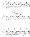
この半導体装置を製造するには、まず、図1(a)に示すように、表面に複数の第1の電極4を備えた回路基板1を用意する。 In order to manufacture this semiconductor device, first, as shown in FIG. 1A, a
その回路基板1の表面にはソルダレジスト層2が形成されており、そのソルダレジスト層2の窓2a内に、銅膜等をパターニングしてなる第1の電極4が形成される。 A solder resist
次いで、図1(b)に示すように、第1の電極4の各々の表面4aを銅に対するエッチング液、例えば塩酸又はクロム酸に曝すことにより、当該表面4aに表面粗さが1μm程度の凹凸を付与する。 Next, as shown in FIG. 1B, the
このような表面4aの粗化処理はウエットエッチングに限定されない。例えば、サンドブラスト、機械研磨、又はアルゴンガスを用いるスパッタエッチングによって粗化を行ってもよい。或いは、電解銅めっきにより第1の電極4を形成するときに、電流密度を調節することにより、電解銅めっき層の疎密をコントロールして表面4aに凹凸を付与するようにしてもよい。 Such roughening treatment of the
次いで、図1(c)に示すように、回路基板1の上側全面にドライフィルムレジストを貼付し、それを露光、現像して第1のレジストパターン6を形成する。 Next, as shown in FIG. 1C, a dry film resist is applied to the entire upper surface of the
その第1のレジストパターン6には複数の窓6aが設けられ、これらの窓6aから第1の電極4の各々が露出する。 The first resist
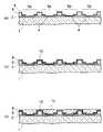
続いて、図2(a)に示すように、第1のレジスト6上と窓6a内とにスパッタ法等によりシード層8として銅膜を0.1μm〜0.5μm程度の厚さに形成する。 Subsequently, as shown in FIG. 2A, a copper film is formed as a
そして、図2(b)に示すように、液温が約90℃に維持されたニッケル用のめっき液中に回路基板1を約2分間浸すことにより、シード層8の表面に無電解めっきにより厚さが0.5μm〜2μm程度のニッケル層を析出させ、そのニッケル層をバリアメタル層10とする。 Then, as shown in FIG. 2B, the surface of the
ここで、ニッケル用のめっき液の中に、リン、タングステン、及びホウ素のいずれかを添加してもよい。これらを添加することで、バリアメタル層10の光沢が増し、バリアメタル層12の美感を高めることができる。 Here, any of phosphorus, tungsten, and boron may be added to the plating solution for nickel. By adding these, the gloss of the
バリアメタル層10は、後述のように、銅と錫の反応を防止する層として機能する。そのような機能を有する層としては、ニッケル層の他にコバルト層や鉄層もあり、これらのいずれか或いはこれらの合金層をバリアメタル層10として形成してもよい。 The
次に、図2(c)に示すように、バリアメタル層10に対して無電解めっきと電解めっきをこの順に行うことにより錫層12を形成する。 Next, as shown in FIG. 2C, the
錫層12の厚さは特に限定されないが、錫層12のうち無電解めっきによる部分の厚さは5μm〜10μm程度とするのが好ましく、電解めっきによる部分は5μm以上とするのが好ましい。 The thickness of the
このように電解めっきを併用することで、無電解めっきのみで錫層12を形成する場合と比較して、錫層12の厚膜化が容易となる。 By using electrolytic plating in this way, it is easy to increase the thickness of the
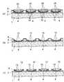
その後に、図3(a)に示すように、第1のレジストパターン6をリフトオフすることにより、第1の電極4の上にのみバリアメタル層10と錫層12とを残す。 Thereafter, as shown in FIG. 3A, the first resist
ここまでの工程により、回路基板1側に対する処理を終了する。 The process for the
この後は、図3(b)に示すように、BGAやCSP等の半導体パッケージ20を用意する。 Thereafter, as shown in FIG. 3B, a
その半導体パッケージ20の表面にはポリイミド層等の保護層24が形成されており、その保護層24の窓内には銅膜等をパターニングしてなる第2の電極22が形成されており、その第2の電極22にははんだバンプ18が接合される。 A
各はんだバンプ18は、例えばその直径が約600μm〜700μmであって、配列ピッチが約1mm〜1.5mmである。 Each
はんだバンプ18の材料は特に限定されない。但し、環境への配慮という観点から、無鉛はんだをはんだバンプ18の材料として用いるのが好ましい。 The material of the
本実施形態で使用し得る無鉛はんだとしては、例えば、Sn-3.0Ag-0.5Cuはんだがある。このはんだは、主成分である96.5重量%の錫に、3.0重量%の銀と0.5重量%の銅とを添加してなる。 As a lead-free solder that can be used in this embodiment, for example, there is Sn-3.0Ag-0.5Cu solder. This solder is obtained by adding 3.0% by weight of silver and 0.5% by weight of copper to 96.5% by weight of tin which is the main component.
これらの添加金属のうち、銀は、はんだバンプ18の材料的強度を向上する材料として知られており、標準的な無鉛はんだに好適に添加される材料である。 Among these additive metals, silver is known as a material that improves the material strength of the
一方、銅は、銅電極とはんだバンプ18とを接合するときに、銅電極中の銅が侵食されてはんだバンプ18に取り込まれるのを阻止する役割を担う。 On the other hand, copper plays a role of preventing the copper in the copper electrode from being eroded and taken into the
なお、添加材料としては、銀と銅の他に、ビスマス、インジウム、亜鉛、及びアンチモンがあり、これらの一以上を上記の無鉛はんだバンプに添加し得る。 In addition to silver and copper, additive materials include bismuth, indium, zinc, and antimony, and one or more of these can be added to the lead-free solder bump.
更に、このように錫を主成分とする無鉛はんだに代えて、ビスマス、インジウム、亜鉛、銀、アンチモン、及び銅のいずれかの金属を主成分とする無鉛はんだバンプを用いてもよい。 Furthermore, instead of the lead-free solder containing tin as a main component, a lead-free solder bump containing a metal as a main component of any one of bismuth, indium, zinc, silver, antimony, and copper may be used.
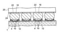
本工程では、半導体パッケージ20を回路基板1側に下ろし、上記のはんだバンプ18を第1の電極4上の錫層12に当接させる。 In this step, the
そして、図4に示すように、リフロー雰囲気中ではんだバンプ18と錫層10とを加熱して溶融することにより、各はんだバンプ18を第1の電極4に接合する。このリフローは、例えば、窒素雰囲気となっているコンベア炉に回路基板1と半導体パッケージ20とを入れ、温度プロファイルの最高温度を250℃に抑えながら、はんだバンプ18をその融点の約217℃以上に約2分間加熱することにより行われる。 Then, as shown in FIG. 4, each
そして、はんだバンプ18が冷却して凝固すると、はんだバンプ18を介して回路基板1と半導体パッケージ20とが電気的かつ機械的に接続される。 When the solder bumps 18 are cooled and solidified, the
なお、このようにはんだバンプ18と錫層12を同時にリフローするのではなく、これらを個別にリフローしてから接合するようにしてもよい。これについては、後述の各実施形態でも同様である。 Note that the solder bumps 18 and the
以上により、本実施形態に係る半導体装置の基本構造が完成した。 Thus, the basic structure of the semiconductor device according to this embodiment is completed.
上記した本実施形態によれば、図4に示すリフロー工程において、はんだバンプ18と共に錫層12も溶融し、溶融した錫層12の一部がはんだバンプ18に取り込まれる。これにより、リフロー前と比較して、はんだバンプ18中の錫の濃度が増大し、相対的に当該はんだバンプ18中の銀の濃度が低下する。 According to the above-described embodiment, in the reflow process shown in FIG. 4, the
銀濃度の低下の度合いは、錫層12の膜厚に依存し、その膜厚が厚い程はんだバンプ18中の銀濃度が低下し易くなる。例えば、錫層12の厚さを10μm以上にすると、はんだバンプ18中の銀濃度が3.0%であったのが、リフローによって2〜2.3%程度と低くすることができ、銀濃度を効果的に低減できる。 The degree of decrease in silver concentration depends on the film thickness of the
既述のように、銀は、はんだバンプの材料的強度を向上する材料として無鉛はんだに標準的に添加される材料である。 As described above, silver is a material that is normally added to lead-free solder as a material that improves the material strength of solder bumps.
とろこが、本願発明者の知見によれば、無鉛はんだバンプ中の銀濃度を低くした方が、はんだバンプのヤング率が低下し、更にその伸び特性も向上して、はんだバンプの材料的強度は向上することが明らかとなった。 According to the knowledge of the present inventor, the lower the silver concentration in the lead-free solder bumps, the lower the Young's modulus of the solder bumps, and the better the elongation characteristics. Was found to improve.
よって、上記のように溶融した錫層12によってはんだバンプ18中の銀濃度を低下させることで、伸び特性が低い無鉛はんだをはんだバンプ18の材料として用いても、リフロー後のはんだバンプ18の材料的強度を向上させることができる。 Therefore, by reducing the silver concentration in the
このように材料的強度が向上することで、無鉛はんだ用の高温のリフロー雰囲気が原因で回路基板1や半導体パッケージ20に反りが生じても、各電極4、22間のはんだバンプ18にクラックが入り難くなる。 By improving the material strength in this manner, even if the
特に、一辺の長さが30mmを超えるような大型の半導体パッケージ20ではリフロー時に反りが顕著に発生するので、本実施形態はこのような大型の半導体パッケージを使用する場合に特に実益がある。 In particular, in a
しかも、錫層12の下に、銅と錫との反応を抑制するバリアメタル層10を形成したので、錫層12中の錫と第1の電極4中の銅との反応が抑えられ、錫層12と第1の電極4との界面にCu6Sn5等からなるCuSn合金層が形成され難くなる。Moreover, since the
CuSn合金層は、その結晶粒が比較的大きいため結晶粒の界面からクラック等が入り易く、固くて脆い材料である。 The CuSn alloy layer is a hard and brittle material because its crystal grains are relatively large, so that cracks and the like are likely to enter from the interface of the crystal grains.
これに対し、本実施形態のようにバリアメタル層10としてニッケル層を形成すると、錫層12と第1の電極4との界面に(Cu,Ni)6Sn5等を含む金属化合物層が形成される。(Cu,Ni)6Sn5は、Cu6Sn5と比較して結晶粒が小さいので、当該結晶粒の界面からクラックが入り難くなり、はんだバンプ18と第1の電極4との接合を落下衝撃等に対して強くすることが可能となる。On the other hand, when a nickel layer is formed as the
更に、図1(b)に示したように、粗化処理によって第1の電極4の表面4aに凹凸を付与したので、回路基板1の主面に平行な方向からはんだバンプ18にクラックが入ろうとしても、上記の凹凸によってクラックの侵入が阻止できるようになる。 Further, as shown in FIG. 1B, the
以下に、本実施形態に関連して本願発明者が行った調査について説明する。 Below, the investigations conducted by the inventors of the present application in relation to the present embodiment will be described.
・第1の調査
本調査では、本実施形態のようにバリアメタル層10としてニッケル層を形成したサンプルを5個作製した。同様に、バリアメタル層10としてコバルト層を形成したサンプルを5個、バリアメタル層10として鉄層を形成したサンプルを5個作製した。-1st investigation In this investigation, five samples which formed the nickel layer as the
また、比較例として、バリアメタル層10と錫層12を省き、更に第1の電極4に対する粗化処理を省略したサンプルも5個作製した。 Further, as a comparative example, five samples were prepared in which the
その後、本実施形態と比較例の各サンプルについて、−55℃の冷却保持時間を30分、125℃の加熱保持時間を30分とし、これら冷却時間と加熱時間とを500回繰り返す温度サイクル試験を行った。 Thereafter, for each sample of the present embodiment and the comparative example, a temperature cycle test was performed by repeating the cooling time and the heating time 500 times with a cooling holding time of −55 ° C. being set to 30 minutes and a heating holding time of 125 ° C. being set to 30 minutes. went.
そして、この試験を終了した後、各々のサンプルの第1の電極4とはんだバンプ18との間の抵抗値を測定し、その抵抗値が許容値を超えたものを不良と判定した。 Then, after this test was completed, the resistance value between the
この結果を表1に示す。 The results are shown in Table 1.

表1に示されるように、本実施形態では、バリアメタル層10としてニッケル層、コバルト層、鉄層のいずれを形成する場合でも不良と判定されたサンプルはなかった。 As shown in Table 1, in this embodiment, there was no sample determined to be defective even when a nickel layer, a cobalt layer, or an iron layer was formed as the
これに対し、バリアメタル層10を形成しない比較例では、5個のサンプルのうち3個のサンプルが不良となった。 On the other hand, in the comparative example in which the
このことから、本実施形態のようにバリアメタル層としてニッケル層等を形成することにより、第1の電極4とはんだバンプ18との接合部が温度変化に対して良好な信頼性を維持できることが確認できた。 From this, by forming a nickel layer or the like as a barrier metal layer as in this embodiment, the joint between the
・第2の調査
本調査では、第1の調査と同様にして、本実施形態と比較例のそれぞれについてサンプルを作製した。-2nd investigation In this investigation, the sample was produced about each of this embodiment and a comparative example like the 1st investigation.
その後、高さ10cmの所から各サンプルを自由落下させ、各サンプルに衝撃を与える試験を200回行った。 Thereafter, each sample was freely dropped from a height of 10 cm, and a test for giving an impact to each sample was performed 200 times.
そして、この試験を終了した後、各々のサンプルの第1の電極4とはんだバンプ18との間の抵抗値を測定し、その抵抗値が許容値を超えたものを不良と判定した。 Then, after this test was completed, the resistance value between the
この結果を表2に示す。 The results are shown in Table 2.
表2に示されるように、本実施形態では、第1の電極4とはんだバンプ18との間の抵抗値が上昇して不良と判定されたサンプルはなかった。 As shown in Table 2, in the present embodiment, there was no sample in which the resistance value between the
一方、バリアメタル層10を形成しない比較例では、5個のサンプルのうち4個のサンプルが不良となった。 On the other hand, in the comparative example in which the
この結果より、本実施形態に従って作製したサンプルでは、第1の電極4とはんだバンプ18との接合部が落下等の耐衝撃性に優れていることが明らかとなった。 From this result, it was clarified that in the sample manufactured according to the present embodiment, the joint between the
(第2実施形態)
第1実施形態では、図3(a)に示したように、第1の電極4の全面にバリアメタル層10を形成したが、本実施形態では以下のようにバリアメタル層10をドット状に形成する。(Second Embodiment)
In the first embodiment, as shown in FIG. 3A, the
図5(a)〜(c)は、本実施形態に係る半導体装置の製造途中の断面図である。なお、これらの図において第1実施形態と同じ要素には第1実施形態と同じ符号を付し、以下ではその説明を省略する。 5A to 5C are cross-sectional views in the middle of manufacturing the semiconductor device according to the present embodiment. In these drawings, the same elements as those of the first embodiment are denoted by the same reference numerals as those of the first embodiment, and description thereof will be omitted below.
この半導体装置を製造するには、まず、第1実施形態で説明した図1(a)〜図2(a)の工程を行う。 To manufacture this semiconductor device, first, the steps shown in FIGS. 1A to 2A described in the first embodiment are performed.
その後、図5(a)に示すように、シード層8の上にドライフィルムレジストを貼付し、それを露光、現像することにより、第1の電極4aの上に複数の細孔を備えた第2のレジストパターン25を形成する。 Thereafter, as shown in FIG. 5 (a), a dry film resist is applied on the
そして、この第2のレジストパターン25をマスクにしながら、液温が約90℃に維持されたニッケル用のめっき液中に回路基板1を約2分間浸す。これにより、シード層8の表面に、バリアメタル層10として厚さが0.5μm〜2μm程度のドット状のニッケル層が形成されることになる。 Then, using the second resist
次に、図5(b)に示すように、第2のレジストパターン25を除去する。 Next, as shown in FIG. 5B, the second resist
この後は、第1実施形態で説明した図2(c)〜図3(a)の工程を行うことにより、図5(c)に示すように、ドット状のバリアメタル層10の上に錫層12を形成する。 Thereafter, by performing the steps of FIG. 2C to FIG. 3A described in the first embodiment, tin is formed on the dot-shaped
そして、図6に示すように、第1実施形態の図4と同様にして、半導体パッケージ20のはんだバンプ18をリフローして錫層12に接合する。 Then, as shown in FIG. 6, the solder bumps 18 of the
以上により、本実施形態に係る半導体装置の基本構造が完成する。 As described above, the basic structure of the semiconductor device according to this embodiment is completed.
本実施形態のようにバリアメタル層10をドット状に形成すると、はんだバンプ18をリフローするとき、錫層12やはんだバンプ18の濡れ性が向上し、これらを良好にはんだ付けすることが可能となる。 When the
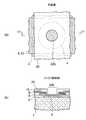
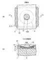
(第3実施形態)
図7〜図9は、本実施形態に係る半導体装置の製造途中の平面図と断面図であり、図10はその断面図である。なお、これらの図において、第1実施形態で説明したのと同じ要素には第1実施形態と同じ符号を付し、以下ではその説明を省略する。(Third embodiment)
7 to 9 are a plan view and a cross-sectional view in the middle of manufacturing the semiconductor device according to this embodiment, and FIG. 10 is a cross-sectional view thereof. In these drawings, the same elements as those described in the first embodiment are denoted by the same reference numerals as those in the first embodiment, and the description thereof is omitted below.
本実施形態では、錫層12の平面形状を以下のように十字型にする。 In the present embodiment, the planar shape of the
この半導体装置を製造するには、まず、第1実施形態の図1(a)〜図2(b)の工程を行う。 In order to manufacture this semiconductor device, first, the steps of FIG. 1A to FIG. 2B of the first embodiment are performed.
次いで、図7(a)、(b)に示すように、回路基板1の上側全面にドライフィルムレジストを貼付し、それを露光、現像して第3のレジストパターン30とする。 Next, as shown in FIGS. 7A and 7B, a dry film resist is applied to the entire upper surface of the
その第3のレジストパターン30は、第1の電極4の上方に、平面形状が十字型の窓30aを有する。 The third resist
次に、図8(a)、(b)に示すように、窓30aに露出するバリアメタル層10の上に、無電解めっきと電解めっきをこの順に行うことにより、平面形状が十字型の錫層12を形成する。 Next, as shown in FIGS. 8A and 8B, by performing electroless plating and electrolytic plating in this order on the
その錫層12のうち、無電解めっきにより形成された部分の厚さは5μm〜10μm程度である。また、電解めっきはシード層8を給電層にして行われ、電解めっきで形成された部分の錫層12の厚さは5μm以上であるのが好ましい。 The thickness of the portion formed by electroless plating in the
この後に、第3のレジストパターン30は除去される。 Thereafter, the third resist
続いて、図9(a)、(b)に示すように、第1のレジストパターン6をリフトオフすることにより、第1の電極4の上にのみバリアメタル層10と錫層12とを残す。 Subsequently, as shown in FIGS. 9A and 9B, the first resist
次いで、図10に示すように、半導体パッケージ20が備えるはんだバンプ18を錫層12に当接させ、窒素雰囲気となっているコンベア炉内においてはんだバンプ18と錫層18とをリフローする。そのリフローでは、はんだバンプ18がその融点である約217℃以上の温度に約2分間加熱される。また、リフローの温度プロファイルの最高温度は250℃である。 Next, as shown in FIG. 10, the solder bumps 18 included in the
ここで、本実施形態のように錫層12の平面形状を十字型にすると、十字型の各辺12a(図9(a)参照)に沿って溶融した錫層12が表面張力によって流動し、第1の電極4の中央付近に錫層12が凝集する。これにより、錫層12内の錫がはんだバンプ18に効率的に取り込まれるようになるので、リフロー前と比較してはんだバンプ18中の錫の濃度を高め易くなる。 Here, when the planar shape of the
そのため、はんだバンプ18中の銀の濃度が相対的に低くなり、Sn-3.0Ag-0.5Cuはんだ等の無鉛材料からなるはんだバンプ18の材料的強度を高めることができるようになる。 Therefore, the silver concentration in the
その後、はんだバンプ18と錫層12が冷却して凝固すると、回路基板1と半導体パッケージ20とがはんだバンプ18を介して電気的かつ機械的に接続される。 Thereafter, when the
以上により、本実施形態に係る半導体装置の基本構造が完成する。 As described above, the basic structure of the semiconductor device according to this embodiment is completed.
上記した本実施形態によれば、錫層12の平面形状を十字型にすることで、溶融した錫層12が表面張力によって第1の電極4の中央付近に凝集するので、錫層12がはんだバンプ18に効率的に取り込まれる。その結果、はんだバンプ18中の銀の濃度が低下し、はんだバンプ18の材料的強度を向上させることが可能となる。 According to the above-described embodiment, since the planar shape of the
以下に、本実施形態に関連して本願発明者が行った調査について説明する。 Below, the investigations conducted by the inventors of the present application in relation to the present embodiment will be described.
・第1の調査
本調査では、上記のように十字型の錫層12を形成したサンプルを5個作製した。-1st investigation In this investigation, five samples which formed the
また、比較例として、バリアメタル層10と錫層12を省き、更に第1の電極4に対する粗化処理を省略したサンプルも5個作製した。 Further, as a comparative example, five samples were prepared in which the
その後、本実施形態と比較例の各サンプルについて、−55℃の冷却保持時間を30分、125℃の加熱保持時間を30分とし、これら冷却保持時間と加熱保持時間とを500回繰り返す温度サイクル試験を行った。 Thereafter, for each sample of this embodiment and the comparative example, a temperature holding cycle of −55 ° C. is set to 30 minutes, a heating holding time of 125 ° C. is set to 30 minutes, and the cooling holding time and the heating holding time are repeated 500 times. A test was conducted.
そして、この試験を終了した後、各々のサンプルの第1の電極4とはんだバンプ18との間の抵抗値を測定し、その抵抗値が許容値を超えたものを不良と判定した。 Then, after this test was completed, the resistance value between the
その結果、本実施形態では不良と判定されたサンプルはなかった。 As a result, no sample was determined to be defective in this embodiment.
一方、比較例では、5個のサンプルのうち3個のサンプルに不良が発生した。 On the other hand, in the comparative example, a defect occurred in three of the five samples.
この結果から、錫層12を十字型にしても、第1の電極4とはんだバンプ18との接合部が温度変化に対して良好な信頼性を維持できることが確認できた。 From this result, it was confirmed that even if the
・第2の調査
本調査では、第1の調査と同様にして、本実施形態と比較例のそれぞれについてサンプルを作製した。-2nd investigation In this investigation, the sample was produced about each of this embodiment and a comparative example like the 1st investigation.
その後、高さが10cmの所から各サンプルを自由落下させ、各サンプルに衝撃を与える試験を200回行った。 Thereafter, each sample was dropped freely from a height of 10 cm, and a test for giving an impact to each sample was performed 200 times.
そして、この試験を終了した後、各々のサンプルの第1の電極4とはんだバンプ18との間の抵抗値を測定し、その抵抗値が許容値を超えたものを不良と判定した。 Then, after this test was completed, the resistance value between the
この結果、本実施形態では不良と判定されたサンプルはなかったのに対し、比較例では5個のサンプルのうち4個のサンプルに不良が発生した。 As a result, in the present embodiment, there was no sample determined to be defective, but in the comparative example, four samples out of five samples had defects.
これにより、本実施形態のように錫層12を十字型にしても、第1の電極4とはんだバンプ18との接合部の耐衝撃性が良好になることが確認できた。 Thus, it was confirmed that even if the
(第4実施形態)
第3実施形態では、図8(a)、(b)を参照して説明したように、十字型の錫層12を無電解めっきと電解めっきにより形成した。(Fourth embodiment)
In the third embodiment, as described with reference to FIGS. 8A and 8B, the
これに対し、本実施形態では、無電解めっきのみで錫層12を形成する。 On the other hand, in this embodiment, the
図11〜図14は、本実施形態に係る半導体装置の製造途中の平面図と断面図であり、図15はその断面図である。なお、これらの図において、第1実施形態で説明したのと同じ要素には第1実施形態と同じ符号を付し、以下ではその説明を省略する。 11 to 14 are a plan view and a cross-sectional view in the middle of manufacturing the semiconductor device according to the present embodiment, and FIG. 15 is a cross-sectional view thereof. In these drawings, the same elements as those described in the first embodiment are denoted by the same reference numerals as those in the first embodiment, and the description thereof is omitted below.
この半導体装置を製造するには、まず、図11(a)、(b)に示すように、第1の電極4の上に無電解めっきによりバリアメタル層10としてニッケル層を0.5μm〜2μm程度の厚さに形成する。 In order to manufacture this semiconductor device, first, as shown in FIGS. 11A and 11B, a nickel layer is formed as a
次いで、図12(a)、(b)に示すように、回路基板1の上側全面にドライレジストフィルムを貼付し、それを露光、現像することにより、第1の電極4の上方に平面形状が十字型の窓30aを備えた第3のレジストパターン30を形成する。 Next, as shown in FIGS. 12 (a) and 12 (b), a dry resist film is applied to the entire upper surface of the
次に、図13(a)、(b)に示すように、第3のレジストパターン30をマスクに用い、窓30aから露出しているバリアメタル層10の上に無電解めっきにより錫層12を1μm〜5μm程度の厚さに形成する。 Next, as shown in FIGS. 13A and 13B, the
そして、図14(a)、(b)に示すように、第3のレジストパターン30を除去する。 Then, as shown in FIGS. 14A and 14B, the third resist
この後は、図15に示すように、半導体パッケージ20のはんだバンプ18を錫層12に当接させ、この状態ではんだバンプ18と錫層12の各々をリフローする。リフローの条件は第3実施形態と同様であって、コンベア炉内において最高温度を250℃にしながら、約217℃の温度でリフローを行う。 Thereafter, as shown in FIG. 15, the solder bumps 18 of the
このとき、第3実施形態で説明したように、溶融した錫層12は、十字型の各辺12a(図14(a)参照)に沿って流動して第1の電極4の中央付近に凝集するので、錫層12がはんだバンプ18に効率的に取り込まれ、はんだバンプ18の銀の濃度を低減できる。 At this time, as described in the third embodiment, the
その後、はんだバンプ18と錫層12が冷却して凝固することで、回路基板1と半導体パッケージ20とがはんだバンプ18を介して電気的かつ機械的に接続され、本実施形態に係る半導体装置の基本構造が得られる。 Thereafter, the solder bumps 18 and the
以上説明した本実施形態によれば、無電解めっきのみによりはんだバンプ18を形成するので、電解めっきも併用する第3実施形態と比較して工程の簡略化を図ることが可能となる。 According to the present embodiment described above, since the solder bumps 18 are formed only by electroless plating, the process can be simplified as compared with the third embodiment that also uses electrolytic plating.
(第5実施形態)
本実施形態では、錫層12の平面形状を以下のように円形にする。(Fifth embodiment)
In the present embodiment, the planar shape of the
図16〜図18は、本実施形態に係る半導体装置の製造途中の平面図と断面図であり、図19はその断面図である。なお、これらの図において、第1実施形態で説明したのと同じ要素には第1実施形態と同じ符号を付し、以下ではその説明を省略する。 16 to 18 are a plan view and a cross-sectional view in the middle of manufacturing the semiconductor device according to this embodiment, and FIG. 19 is a cross-sectional view thereof. In these drawings, the same elements as those described in the first embodiment are denoted by the same reference numerals as those in the first embodiment, and the description thereof is omitted below.
この半導体装置を製造するには、まず、第1実施形態に従って既述の図2(b)の断面構造を得る。 To manufacture this semiconductor device, first, the cross-sectional structure shown in FIG. 2B is obtained according to the first embodiment.
そして、図16(a)、(b)に示すように、回路基板1の上側全面にドライフィルムレジストを貼付し、それを露光、現像して第3のレジストパターン30とする。 Then, as shown in FIGS. 16A and 16B, a dry film resist is applied to the entire upper surface of the
その第3のレジストパターン30は、第1の電極4の上方に、当該第1の電極4よりも小さい平面形状が円形の窓30bを備える。 The third resist
次いで、図17(a)、(b)に示すように、第3のレジストパターン30をマスクに使用しながら、窓30bから露出するバリアメタル層10の上に錫層12を形成する。 Next, as shown in FIGS. 17A and 17B, the
錫層12は無電解めっきと電解めっきとをこの順に行うことで形成され、無電解めっきにより形成された部分の厚さは5μm〜10μm程度、そして電解めっきにより形成された部分の厚さは5μm以上とするのが好ましい。また、電解めっきに際しては、シード層8が給電層として使用される。 The
その錫層12の平面形状は、窓30bを反映し、第1の電極4よりも小さな円形となる。 The planar shape of the
この後に、第3のレジストパターン30は除去される。 Thereafter, the third resist
続いて、図18(a)、(b)に示すように、第1のレジストパターン6をリフトオフすることにより、第1の電極4の上にのみバリアメタル層10と錫層12とを残す。 Subsequently, as shown in FIGS. 18A and 18B, the first resist
次いで、図19に示すように、半導体パッケージ20のはんだバンプ18を錫層12に当接させ、この状態でコンベア炉内において温度プロファイルの最高温度を250℃に設定し、はんだバンプ18と錫層12を加熱して溶融する。 Next, as shown in FIG. 19, the solder bumps 18 of the
このとき、本実施形態では第1の電極4よりも小さな円形に錫層12を形成したので、溶融した錫層12がはんだバンプ18に簡単に取り込まれ、溶融した錫層12が第1の電極4の周縁部に濡れ広がるのを抑制できる。 At this time, since the
これにより、錫層12の大部分がはんだバンプ18に取り込まれるようになるので、はんだバンプ18中の銀の濃度を効率的に低下させることができ、はんだバンプ18の材料的強度を向上させることができる。 As a result, most of the
その後、錫層12とはんだバンプ18が冷却して凝固することで、半導体パッケージ20と回路基板1とがはんだバンプ18を介して電気的かつ機械的に接続され、本実施形態に係る半導体装置の基本構造が完成する。 Thereafter, the
以上説明した本実施形態によれば、錫層12の平面形状を第1の電極4よりも小さな円形にすることで、錫層12とはんだバンプ18をリフローする際、はんだバンプ18に溶融した錫層12をすぐさま取り込むことができる。 According to the present embodiment described above, the
その結果、溶融した錫層12が第1の電極4の周縁部に無駄に広がるのを防止でき、はんだバンプ18中の銀の濃度を効果的に低減して当該はんだバンプ18の材料的強度を高めることが可能となる。 As a result, it is possible to prevent the melted
以上、各実施形態について詳細に説明したが、各実施形態は上記に限定されない。 As mentioned above, although each embodiment was described in detail, each embodiment is not limited to the above.
例えば、上記では、回路基板1と半導体パッケージ20とを接続するのにはんだバンプ18を使用したが、接続対象はこれに限定されず、半導体素子等の半導体部品と回路基板1とをはんだバンプ18で接続するようにしてもよい。 For example, in the above, the solder bumps 18 are used to connect the
更に、その半導体部品の接続対象となる下地は回路基板1に限定されず、回路基板1に代えて半導体素子を用いてもよい。 Further, the base to be connected to the semiconductor component is not limited to the
以上説明した各実施形態に関し、更に以下の付記を開示する。 The following additional notes are disclosed for each embodiment described above.
(付記1) 銅を含む第1の電極が表面に形成された下地と、
前記第1の電極の表面に形成され、前記銅と錫との反応を抑制するバリアメタル層と、
前記バリアメタル層の上に形成された錫層と、
前記錫層を介して前記第1の電極に接合された無鉛はんだバンプと、
前記無鉛はんだバンプと接合された第2の電極を備えた半導体部品と、
を有することを特徴とする半導体装置。(Additional remark 1) The base | substrate with which the 1st electrode containing copper was formed in the surface,
A barrier metal layer formed on the surface of the first electrode to suppress a reaction between the copper and tin;
A tin layer formed on the barrier metal layer;
A lead-free solder bump joined to the first electrode via the tin layer;
A semiconductor component comprising a second electrode joined to the lead-free solder bump;
A semiconductor device comprising:
(付記2) 前記バリアメタル層は、ニッケル、コバルト、及び鉄のいずれか、或いはこれらの合金を含むことを特徴とする付記1に記載の半導体装置。 (Supplementary note 2) The semiconductor device according to
(付記3) 前記第1の電極の表面に、粗化処理が施されていることを特徴とする付記1又は付記2に記載の半導体装置。 (Additional remark 3) The semiconductor device of
(付記4) 前記無鉛はんだバンプは、錫を主成分とし、ビスマス、インジウム、亜鉛、銀、アンチモン、及び銅のいずれかを添加材料として含むことを特徴とする付記1〜3のいずれかに記載の半導体装置。 (Additional remark 4) The said lead-free solder bump has tin as a main component, and contains either bismuth, indium, zinc, silver, antimony, and copper as an additive material, Any one of additional remark 1-3 characterized by the above-mentioned. Semiconductor device.
(付記5) 下地の表面に形成された銅を含む第1の電極の上に、前記銅と錫との反応を抑制するバリアメタル層を形成する工程と、
前記バリアメタル層の上に錫層を形成する工程と、
半導体部品の第2の電極に接合された無鉛はんだバンプを前記錫層に当接させ、該バンプを加熱して溶融することにより、前記第1の電極と前記第2の電極とを前記バンプを介して接続する工程と、
を有することを特徴とする半導体装置の製造方法。(Additional remark 5) The process of forming the barrier metal layer which suppresses reaction with the said copper and tin on the 1st electrode containing copper formed in the surface of the foundation | substrate,
Forming a tin layer on the barrier metal layer;
A lead-free solder bump bonded to the second electrode of the semiconductor component is brought into contact with the tin layer, and the bump is heated and melted, whereby the first electrode and the second electrode are bonded to the bump. Connecting via,
A method for manufacturing a semiconductor device, comprising:
(付記6) 前記バリアメタル層を形成する工程において、ニッケル、コバルト、及び鉄のいずれか、或いはこれらの合金を含む層を前記バリアメタル層として形成することを特徴とする付記5に記載の半導体装置の製造方法。 (Supplementary note 6) The semiconductor according to supplementary note 5, wherein in the step of forming the barrier metal layer, a layer containing any one of nickel, cobalt, and iron, or an alloy thereof is formed as the barrier metal layer. Device manufacturing method.
(付記7) 前記バリアメタル層を形成する工程において、前記第1の電極の表面に前記バリアメタル層をドット状に形成することを特徴とする付記5又は付記6に記載の半導体装置の製造方法。 (Supplementary note 7) In the step of forming the barrier metal layer, the barrier metal layer is formed in a dot shape on the surface of the first electrode. The method of manufacturing a semiconductor device according to supplementary note 5 or
(付記8) 前記錫層を形成する工程において、十字型の平面形状に前記錫層を形成することを特徴とする付記5又は付記6に記載の半導体装置の製造方法。 (Additional remark 8) The manufacturing method of the semiconductor device of Additional remark 5 or
(付記9) 前記錫層を形成する工程において、前記第1の電極よりも小さな円形の平面形状に前記錫層を形成することを特徴とする付記5又は付記6に記載の半導体装置の製造方法。 (Supplementary note 9) In the step of forming the tin layer, the tin layer is formed in a circular planar shape smaller than the first electrode. The method of manufacturing a semiconductor device according to supplementary note 5 or
1…回路基板、2…ソルダレジスト層、2a…窓、4…第1の電極、4a…表面、6…第1のレジストパターン、6a…窓、8…シード層、10…バリアメタル層、12…錫層、12a…辺、18…はんだバンプ、20…半導体パッケージ、22…第2の電極、24…保護層、25…第2のレジストパターン、30…第3のレジストパターン、30a、30b…窓。DESCRIPTION OF
Claims (2)
Translated fromJapanese前記バリアメタル層の上に、平面形状が十字型の錫層を形成する工程と、
半導体部品の第2の電極に接合された、銀を含む無鉛はんだバンプを前記錫層に当接させ、前記錫層が前記バリアメタル層の上に直接形成されている状態で該バンプを加熱して溶融することにより、前記第1の電極と前記第2の電極とを前記バンプを介して接続する工程と、
を有することを特徴とする半導体装置の製造方法。Forming a barrier metal layer, which is a nickel layer that suppresses a reaction between the copper and tin, on the first electrode including copper formed on the surface of the base and having the surface roughened; ,
Forming across-shaped tin layer on the barrier metal layer;
A lead-free solder bumpcontaining silver joined to the second electrode of the semiconductor component is brought into contact with the tin layer, and the bump is heated in a state where the tin layer is directly formed on the barrier metal layer. Connecting the first electrode and the second electrode via the bumps by melting them,
A method for manufacturing a semiconductor device, comprising:
Priority Applications (1)
| Application Number | Priority Date | Filing Date | Title |
|---|---|---|---|
| JP2009248482AJP5476926B2 (en) | 2009-10-29 | 2009-10-29 | Manufacturing method of semiconductor device |
Applications Claiming Priority (1)
| Application Number | Priority Date | Filing Date | Title |
|---|---|---|---|
| JP2009248482AJP5476926B2 (en) | 2009-10-29 | 2009-10-29 | Manufacturing method of semiconductor device |
Publications (2)
| Publication Number | Publication Date |
|---|---|
| JP2011096803A JP2011096803A (en) | 2011-05-12 |
| JP5476926B2true JP5476926B2 (en) | 2014-04-23 |
Family
ID=44113423
Family Applications (1)
| Application Number | Title | Priority Date | Filing Date |
|---|---|---|---|
| JP2009248482AExpired - Fee RelatedJP5476926B2 (en) | 2009-10-29 | 2009-10-29 | Manufacturing method of semiconductor device |
Country Status (1)
| Country | Link |
|---|---|
| JP (1) | JP5476926B2 (en) |
Families Citing this family (4)
| Publication number | Priority date | Publication date | Assignee | Title |
|---|---|---|---|---|
| KR20130033863A (en)* | 2011-09-27 | 2013-04-04 | 삼성전기주식회사 | Semiconductor package and method for manufacturing thereof |
| JP5820991B2 (en) | 2012-01-17 | 2015-11-24 | パナソニックIpマネジメント株式会社 | Semiconductor device manufacturing method and semiconductor device |
| JP6076020B2 (en)* | 2012-02-29 | 2017-02-08 | ルネサスエレクトロニクス株式会社 | Semiconductor device and manufacturing method of semiconductor device |
| CN116313834B (en)* | 2023-05-24 | 2023-09-12 | 江西兆驰半导体有限公司 | Wafer level packaging method and wafer level packaging structure |
Family Cites Families (9)
| Publication number | Priority date | Publication date | Assignee | Title |
|---|---|---|---|---|
| JP3475147B2 (en)* | 2000-04-17 | 2003-12-08 | 株式会社タムラ製作所 | Solder connection |
| JP2002026063A (en)* | 2000-07-05 | 2002-01-25 | Seiko Epson Corp | Semiconductor device pad structure and method of manufacturing the same |
| JP2004072043A (en)* | 2002-08-09 | 2004-03-04 | Hitachi Maxell Ltd | Semiconductor wafer, semiconductor chip, semiconductor device and method of manufacturing the same |
| KR100495184B1 (en)* | 2002-12-02 | 2005-06-14 | 엘지마이크론 주식회사 | A tape substrate and tin plating method of the tape substrate |
| JP4010311B2 (en)* | 2004-09-06 | 2007-11-21 | セイコーエプソン株式会社 | Semiconductor device and manufacturing method of semiconductor device |
| JP4868892B2 (en)* | 2006-03-02 | 2012-02-01 | 富士通株式会社 | Plating method |
| JP4748317B2 (en)* | 2006-08-31 | 2011-08-17 | Tdk株式会社 | Terminal electrodes and electronic components |
| WO2009002343A1 (en)* | 2007-06-28 | 2008-12-31 | Agere Systems Inc. | Inhibition of copper dissolution for lead-free soldering |
| JP4547411B2 (en)* | 2007-10-05 | 2010-09-22 | 富士通株式会社 | Semiconductor device and manufacturing method of semiconductor device |
- 2009
- 2009-10-29JPJP2009248482Apatent/JP5476926B2/ennot_activeExpired - Fee Related
Also Published As
| Publication number | Publication date |
|---|---|
| JP2011096803A (en) | 2011-05-12 |
Similar Documents
| Publication | Publication Date | Title |
|---|---|---|
| JP4428448B2 (en) | Lead-free solder alloy | |
| CN103547408B (en) | Lead-free solder ball | |
| KR101317019B1 (en) | Soldering method and related device for improved resistance to brittle fracture | |
| KR101355694B1 (en) | Solder ball for semiconductor mounting and electronic member | |
| KR101345940B1 (en) | Solder, soldering method, and semiconductor device | |
| KR20070077613A (en) | Bonding method at low temperature, semiconductor package mounting method using the same, and substrate bonding structure thereby | |
| KR20140015242A (en) | Lead-free solder ball | |
| US7132020B2 (en) | Solder for use on surfaces coated with nickel by electroless plating | |
| WO2014115858A1 (en) | Wiring substrate and method for manufacturing same | |
| JP2003230980A (en) | Electronic member having lead-free solder alloy, solder ball and solder bump | |
| JP5476926B2 (en) | Manufacturing method of semiconductor device | |
| JP4831502B2 (en) | Connection terminal balls and connection terminals with excellent drop impact resistance and electronic components | |
| WO2004105053A1 (en) | Conductive ball, method of forming electrode of electronic part, electronic part and electronic equipment | |
| TWI540015B (en) | Lead free solder ball | |
| JP4888096B2 (en) | Semiconductor device, circuit wiring board, and manufacturing method of semiconductor device | |
| JP5083000B2 (en) | Electronic component device and method of manufacturing electronic component device | |
| KR101009192B1 (en) | Bump Structure of Semiconductor Device and Manufacturing Method Thereof | |
| US20250001529A1 (en) | Solder alloy, solder joint, and semiconductor package including solder joint | |
| JP2008218483A (en) | Semiconductor device and manufacturing method thereof | |
| Atiqah et al. | the Intermetallic Compound (IMC) Growth in Solder Joints | |
| TWI419280B (en) | Electronic device for preventing diffusion of metals | |
| JP2009095865A (en) | Nickel-carried solder ball | |
| Atiqah et al. | the Intermetallic Compound (IMC) | |
| JP2012019244A (en) | Semiconductor device, circuit wiring board, and method of manufacturing semiconductor device |
Legal Events
| Date | Code | Title | Description |
|---|---|---|---|
| A621 | Written request for application examination | Free format text:JAPANESE INTERMEDIATE CODE: A621 Effective date:20120720 | |
| A977 | Report on retrieval | Free format text:JAPANESE INTERMEDIATE CODE: A971007 Effective date:20130215 | |
| A131 | Notification of reasons for refusal | Free format text:JAPANESE INTERMEDIATE CODE: A131 Effective date:20130219 | |
| A521 | Written amendment | Free format text:JAPANESE INTERMEDIATE CODE: A523 Effective date:20130419 | |
| A131 | Notification of reasons for refusal | Free format text:JAPANESE INTERMEDIATE CODE: A131 Effective date:20131022 | |
| A521 | Written amendment | Free format text:JAPANESE INTERMEDIATE CODE: A523 Effective date:20131216 | |
| TRDD | Decision of grant or rejection written | ||
| A01 | Written decision to grant a patent or to grant a registration (utility model) | Free format text:JAPANESE INTERMEDIATE CODE: A01 Effective date:20140114 | |
| A61 | First payment of annual fees (during grant procedure) | Free format text:JAPANESE INTERMEDIATE CODE: A61 Effective date:20140127 | |
| R150 | Certificate of patent or registration of utility model | Ref document number:5476926 Country of ref document:JP Free format text:JAPANESE INTERMEDIATE CODE: R150 | |
| LAPS | Cancellation because of no payment of annual fees |