JP5465828B2 - Substrate processing apparatus and semiconductor device manufacturing method - Google Patents
Substrate processing apparatus and semiconductor device manufacturing methodDownload PDFInfo
- Publication number
- JP5465828B2 JP5465828B2JP2007257768AJP2007257768AJP5465828B2JP 5465828 B2JP5465828 B2JP 5465828B2JP 2007257768 AJP2007257768 AJP 2007257768AJP 2007257768 AJP2007257768 AJP 2007257768AJP 5465828 B2JP5465828 B2JP 5465828B2
- Authority
- JP
- Japan
- Prior art keywords
- lamp
- substrate
- heating
- heating unit
- processing chamber
- Prior art date
- Legal status (The legal status is an assumption and is not a legal conclusion. Google has not performed a legal analysis and makes no representation as to the accuracy of the status listed.)
- Active
Links
Images


Landscapes
- Plasma Technology (AREA)
- Drying Of Semiconductors (AREA)
Description
Translated fromJapanese本発明は、プラズマを発生させ、シリコンウェーハ等の基板表面に対して、酸化処理、不純物の拡散、薄膜の生成、エッチング等のプラズマ処理を施して半導体装置を製造する半導体製造装置に関するものである。 The present invention relates to a semiconductor manufacturing apparatus for manufacturing a semiconductor device by generating plasma and subjecting the surface of a substrate such as a silicon wafer to plasma processing such as oxidation, impurity diffusion, thin film generation, and etching. .
基板にプラズマ処理を施す半導体製造装置として、電界と磁界により高密度プラズマを生成できる変形マグネトロン型プラズマ処理装置(以下、MMT装置)がある(例えば、特許文献1参照)。 As a semiconductor manufacturing apparatus that performs plasma processing on a substrate, there is a modified magnetron type plasma processing apparatus (hereinafter referred to as MMT apparatus) that can generate high-density plasma by an electric field and a magnetic field (see, for example, Patent Document 1).
該MMT装置は、気密性を確保した反応室を有し、反応室に基板を収納し、所要の加熱手段で基板を加熱し、反応室の上部から処理ガスをシャワー状に供給し、反応室内を所定の処理圧に維持する。 The MMT apparatus has a reaction chamber in which airtightness is ensured, the substrate is accommodated in the reaction chamber, the substrate is heated by a required heating means, and a processing gas is supplied in a shower form from the upper part of the reaction chamber. Is maintained at a predetermined processing pressure.
反応室の外周に設けたリング状電極に高周波電力を供給して電界を形成すると共に、リング状電極の周囲に設けた磁石により磁界をかけてマグネトロン放電を起こす。リング状電極から放出された電子が、ドリフトしながらサイクロイド運動を続けて周回することにより長寿命となって電離生成率を高めるので、高密度プラズマを生成できる。このプラズマにより成膜用ガスを励起分解させて化学的反応を起こし、基板表面に薄膜を形成する等の基板処理を行う。 A high frequency power is supplied to a ring electrode provided on the outer periphery of the reaction chamber to form an electric field, and a magnetron discharge is generated by applying a magnetic field by a magnet provided around the ring electrode. The electrons emitted from the ring-shaped electrode continue to circulate in a cycloidal motion while drifting, so that the lifetime is increased and the ionization generation rate is increased, so that high-density plasma can be generated. Substrate processing such as forming a thin film on the surface of the substrate by performing chemical reaction by exciting and decomposing the deposition gas with this plasma is performed.
基板処理の過程で、基板は150℃〜850℃に加熱されるが、加熱手段の1つとして赤外光を発するハロゲンランプが用いられる。 In the course of substrate processing, the substrate is heated to 150 ° C. to 850 ° C. A halogen lamp that emits infrared light is used as one of the heating means.
又、複数のハロゲンランプが基板と対向する様に平面的に配置され、ハロゲンランプが発する赤外光による輻射加熱により基板が加熱されている。又、輻射加熱を効率よく行う様に、ハロゲンランプの反基板側には反射板、或は反射面が形成され、ハロゲンランプから基板と反対側に発せられる赤外光が基板に向けられる様になっている。 A plurality of halogen lamps are arranged in a plane so as to face the substrate, and the substrate is heated by radiant heating by infrared light emitted from the halogen lamp. In order to efficiently perform radiant heating, a reflection plate or reflection surface is formed on the opposite side of the halogen lamp so that infrared light emitted from the halogen lamp to the opposite side of the substrate is directed to the substrate. It has become.
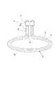
図4は、ハロゲンランプの一例を示しており、図4で示されるハロゲンランプ1は基板と対向する加熱部2がリング状となっている。 FIG. 4 shows an example of a halogen lamp, and the
前記ハロゲンランプ1は石英管3に発熱線4を収納した構造を有しており、前記石英管3はリング状部分5と該リング状部分5に連続し、該リング状部分5に対し垂直に屈曲した垂直端部6から成り、該垂直端部6が反射板、或は反応室の天井部を気密に貫通して上端が露出し、前記垂直端部6で前記ハロゲンランプ1が支持される様になっている。 The
前記リング状部分5には前記発熱線4が収納され前記加熱部2を構成し、前記垂直端部6には非発熱体であるリード線8が収納される。又、前記垂直端部6の上端には絶縁端子部7が設けられ、前記リード線8が支持され、該リード線8は金属箔9を介して前記発熱線4に溶接され、前記リード線8より前記発熱線4に電力が供給される様になっている。 The heating portion 4 is accommodated in the ring-
上記ハロゲンランプ1を発熱体とする加熱手段では、前記垂直端部6には非発熱体である前記リード線8が収納され、前記垂直端部6からは発熱しない様にされ、該垂直端部6からの熱で反射板、天井部、ランプ固定部等の構造部が加熱されない様に配慮されている。 In the heating means using the
ところが、前記リング状部分5に対しては反射板が設けられているが、前記垂直端部6部分については、特に反射板等は設けられていないので、前記加熱部2からの輻射熱が前記垂直端部6を通して、天井部、ランプ固定部等の構造部を加熱する現象を生じていた。 However, a reflector is provided for the ring-
この為、前記垂直端部6の支持部、或は貫通箇所について耐熱材料を用いる等耐熱対策、耐熱構造が必要となっていた。 For this reason, a heat-resistant measure and a heat-resistant structure are required, such as using a heat-resistant material for the support portion of the
尚、前記ハロゲンランプ1が棒状のものである場合に於いても、両端には垂直端部6、即ち固定部が形成され、同様な問題を有していた。 Even when the
本発明は斯かる実情に鑑み、ハロゲンランプの両端部、及び両端部の固定部、隣接する構造部が、加熱部からの熱輻射によって加熱されない様にしたものである。 In view of such a situation, the present invention is configured such that both ends of the halogen lamp, the fixed portions of the both ends, and the adjacent structure are not heated by heat radiation from the heating section.
本発明は、基板加熱手段としてランプ加熱ユニットを具備する半導体製造装置に於いて、前記ランプ加熱ユニットのランプが基板に対向する加熱部と該加熱部に連続する端部を具備し、該端部は該端部からの輻射熱を反射する端部カバーで覆われた半導体製造装置に係るものである。 The present invention provides a semiconductor manufacturing apparatus including a lamp heating unit as a substrate heating means, wherein the lamp of the lamp heating unit includes a heating portion facing the substrate and an end continuous to the heating portion. Is related to a semiconductor manufacturing apparatus covered with an end cover that reflects radiant heat from the end.
本発明によれば、基板加熱手段としてランプ加熱ユニットを具備する半導体製造装置に於いて、前記ランプ加熱ユニットのランプが基板に対向する加熱部と該加熱部に連続する端部を具備し、該端部は該端部からの輻射熱を反射する端部カバーで覆われたので、ランプの両端部、及び両端部の固定部、隣接する構造部が、加熱部からの熱輻射によって加熱されることが防止されるという優れた効果を発揮する。 According to the present invention, in a semiconductor manufacturing apparatus comprising a lamp heating unit as a substrate heating means, the lamp of the lamp heating unit comprises a heating part facing the substrate and an end continuous to the heating part, Since the end portion is covered with an end cover that reflects the radiant heat from the end portion, both end portions of the lamp, the fixed portions at both end portions, and the adjacent structure portion are heated by heat radiation from the heating portion. Demonstrate the excellent effect of preventing.
以下、図面を参照しつつ本発明を実施する為の最良の形態を説明する。尚、図1〜3中、図4と同等のものには同符号を付してある。 The best mode for carrying out the present invention will be described below with reference to the drawings. 1 to 3 that are the same as those in FIG.
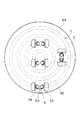
先ず、図1により、本発明が実施されるプラズマを用いた半導体製造装置の一例であり、変形マグネトロン型プラズマ源(Modified Magnetron Typed Plasma Source)を用いてウェーハ等の基板をプラズマ処理するMMT装置11について説明する。 First, FIG. 1 shows an example of a semiconductor manufacturing apparatus using plasma in which the present invention is implemented, and an
該MMT装置11は、処理容器12を有し、該処理容器12は、第1の容器であるドーム型の上側容器13と第2の容器である碗型の下側容器14により形成され、前記上側容器13は前記下側容器14の上に被せられ、該下側容器14と前記上側容器13によって気密な処理室15が画成される。 The
前記上側容器13は酸化アルミニウム又は石英等の非金属材料で形成されており、前記下側容器14は金属材料、例えばアルミニウムで形成されている。又、前記処理容器12の天井面には光透過性窓部16が配設され、該光透過性窓部16に関して前記処理容器12外側に第2の加熱部であるランプ加熱ユニット17が設けられている。 The
又、該ランプ加熱ユニット17に対峙して第1の加熱部を搭載するヒータ一体型の基板保持具(基板保持手段)であるサセプタ18が設けられ、該サセプタ18を窒化アルミニウムやセラミックス又は石英等の非金属材料で構成することによって、基板処理の際に膜中に取込まれる金属汚染を低減している。 Further, a
シャワーヘッド19は、前記処理容器12の上部に設けられ、リング状の枠体21と、前記光透過性窓部16と、ガス導入口22と、バッファ室23と、開口24と、遮蔽プレート25と、ガス吹出口26とを備えている。前記バッファ室23は、前記ガス導入口22より導入されたガスを分散する為の分散空間として機能する。 The
前記ガス導入口22には、ガスを供給するガス供給管27が接続されており、該ガス供給管27は、開閉弁であるバルブ28、流量制御器(流量制御手段)であるマスフローコントローラ29を介して反応ガス31のガスボンベ(図示せず)に繋がっている。 A
前記シャワーヘッド19から反応ガス31が前記処理室15に供給され、又、前記サセプタ18の周囲から前記処理室15の底方向へ基板処理後のガスが流れる様に前記下側容器14の側壁にガスを排気するガス排気口32が設けられている。該ガス排気口32にはガス排気管33が接続されており、該ガス排気管33は、圧力調整器であるAPC34、開閉弁であるバルブ35を介して排気装置である真空ポンプ36に接続されている。 The
供給される反応ガス31を励起させる放電機構(放電用電極)として、筒状、例えば円筒状に形成された第1の電極である筒状電極37が設けられる。該筒状電極37は前記処理容器12(上側容器13)の外周に設置されて前記処理室15のプラズマ生成領域38を囲んでいる。前記筒状電極37にはインピーダンスの整合を行う整合器39を介して高周波電力を印加する高周波電源41が接続されている。 As a discharge mechanism (discharge electrode) that excites the supplied
尚、前記筒状電極37、前記整合器39、前記高周波電源41等はプラズマ生成部を構成する。 The
又、筒状、例えば円筒状に形成された磁界形成機構(磁界形成手段)である筒状磁石43は筒状の永久磁石となっている。該筒状磁石43は、前記筒状電極37の外表面の上下端近傍に配置される。上下の筒状磁石43,43は、前記処理室15の半径方向に沿った両端(内周端と外周端)に磁極を持ち、上下の筒状磁石43,43の磁極の向きが逆向きになる様設定されている。従って、内周部の磁極同士が異極となっており、これにより、前記筒状電極37の内周面に沿って円筒軸方向に磁力線を形成する様になっている。 Further, the
前記処理室15の底側中央には、基板であるウェーハ44を保持する為の基板保持具(基板保持手段)として前記サセプタ18が配置されている。該サセプタ18は、例えば窒化アルミニウムやセラミックス、又は石英等の非金属材料で形成され、内部に加熱機構(加熱手段)としてのヒータ(図示せず)が一体的に埋込まれており、ウェーハ44を加熱できる様になっている。ヒータは、電力が印加されてウェーハ44を700℃程度に迄加熱できる様になっている。 In the center of the bottom side of the
又、前記サセプタ18の内部には、更にインピーダンスを変化させる為の電極である第2の電極(図示せず)も装備されており、該第2の電極がインピーダンス可変機構45を介して接地されている。該インピーダンス可変機構45は、コイルや可変コンデンサから構成され、コイルのパターン数や可変コンデンサの容量値を制御することによって、上記電極及び前記サセプタ18を介してウェーハ44の電位を制御できる様になっている。 The
ウェーハ44をマグネトロン型プラズマ源でのマグネトロン放電により処理する為の処理炉46は、少なくとも前記処理室15、前記処理容器12、前記サセプタ18、前記筒状電極37、前記筒状磁石43、前記シャワーヘッド19、及び前記ガス排気口32から構成されており、前記処理室15でウェーハ44をプラズマ処理することが可能となっている。 The
前記筒状電極37及び前記筒状磁石43の周囲には、前記筒状電極37及び前記筒状磁石43で形成される電界や磁界を外部環境や他処理炉等の装置に悪影響を及ぼさない様に、電界や磁界を有効に遮蔽する遮蔽ケース47が設けられている。 Around the
前記サセプタ18は前記下側容器14と絶縁され、前記サセプタ18を昇降させるサセプタ昇降機構(昇降手段)48が設けられている。又前記サセプタ18には貫通孔49が設けられ、前記下側容器14底面にはウェーハ44を突上げる為のウェーハ突上げピン51が少なくとも3箇所に設けられている。前記サセプタ昇降機構48により前記サセプタ18が降下させられた時には前記ウェーハ突上げピン51が前記サセプタ18と非接触な状態で前記貫通孔49を突抜ける様な位置関係となる様、前記貫通孔49及び前記ウェーハ突上げピン51が配置される。 The
前記下側容器14の側壁には仕切弁となるゲートバルブ52が設けられ、開いている時には搬送機構(搬送手段)(図示せず)により前記処理室15に対してウェーハ44を搬入、又は搬出することができ、閉まっている時には前記処理室15を気密に閉じることができる。 A
又、制御部(制御手段)としてのコントローラ53は信号線Aを通じて前記APC34、前記バルブ35、前記真空ポンプ36を、信号線Bを通じて前記サセプタ昇降機構48を、信号線Cを通じて前記ゲートバルブ52を、信号線Dを通じて前記整合器39、前記高周波電源41を、信号線Eを通じて前記マスフローコントローラ29、前記バルブ28を、更に図示しない信号線を通じて前記サセプタ18に埋込まれたヒータや前記インピーダンス可変機構45を、信号線Fを通じて前記ランプ加熱ユニット17をそれぞれ制御する様構成されている。 The
次に上記の様な構成の処理炉を用いて、半導体デバイスの製造工程の一工程として、ウェーハ44表面に対し、又はウェーハ44上に形成された下地膜の表面に対し所定のプラズマ処理を施す方法について説明する。尚、以下の説明に於いて、MMT装置11を構成する各部の動作は前記コントローラ53により制御される。 Next, using the processing furnace having the above-described configuration, a predetermined plasma process is performed on the surface of the wafer 44 or the surface of the base film formed on the wafer 44 as one step of the semiconductor device manufacturing process. A method will be described. In the following description, the operation of each part constituting the
ウェーハ44は前記処理室15の外部から搬送機構(図示せず)によって前記処理室15に搬入され、前記サセプタ18上に搬送される。この搬送動作の詳細は次の通りである。 The wafer 44 is transferred from the outside of the
前記サセプタ18が基板搬送位置迄降下し、前記ウェーハ突上げピン51の先端が前記貫通孔49を貫通する。この時前記サセプタ18表面よりも所定の高さ分だけ前記突上げピン51が突出された状態となる。次に、前記ゲートバルブ52が開かれ搬送機構(図示せず)によってウェーハ44を前記ウェーハ突上げピン51の先端に載置する。 The
前記搬送機構が前記処理室15外へ退避すると、前記ゲートバルブ52が閉じられる。前記サセプタ18が前記サセプタ昇降機構48により上昇すると、前記サセプタ18上面にウェーハ44を載置することができ、更にウェーハ44を処理する位置迄上昇させる。 When the transfer mechanism is retracted out of the
前記サセプタ18に埋込まれたヒータは予め加熱されており、搬入されたウェーハ44を150℃〜700℃の範囲の内、所定のウェーハ処理温度に加熱する。 The heater embedded in the
前記真空ポンプ36、及び前記APC34を用いて前記処理室15の圧力を1Pa〜200Paの範囲の内、所定の圧力に維持する。 Using the
ウェーハ44の温度が処理温度に達し、安定化したら、前記ガス導入口22から前記遮蔽プレート25の前記ガス吹出口26を介して、窒素含有ガスをウェーハ44の上面(処理面)に向けて導入する。この時のガス流量は所定の流量(例えば100sccm〜500sccm)とする。 When the temperature of the wafer 44 reaches the processing temperature and stabilizes, a nitrogen-containing gas is introduced from the
同時に前記筒状電極37に前記高周波電源41から前記整合器39を介して高周波電力を印加する。印加する電力は、100W〜1000Wの範囲の内、所定の出力値を投入する。この時前記インピーダンス可変機構45は予め所望のインピーダンス値となる様に制御しておく。 At the same time, high frequency power is applied to the
前記筒状磁石43,43の磁界の影響を受けてマグネトロン放電が発生し、ウェーハ44の上方空間に電荷をトラップして前記プラズマ生成領域38に高密度プラズマが生成される。そして、生成された高密度プラズマにより、前記サセプタ18上のウェーハ44の表面にプラズマ処理が施される。 A magnetron discharge is generated under the influence of the magnetic field of the
プラズマ処理が終わると、前記筒状電極37への電力供給を停止し、窒素含有ガスを前記処理室15から排気する。排気した後、ウェーハ44は、搬送機構(図示せず)を用いて、基板搬入と逆の手順で前記処理室15外へ搬送される。 When the plasma processing is finished, the power supply to the
次に、図2、図3により前記ランプ加熱ユニット17について説明する。尚、図2では、ハロゲンランプ1の垂直端部6の支持部について、支持構造を明確にする為、便宜的に位置と向きとを変更して示している。 Next, the
アルミ製の反射ブロック55の下面には多重同心円上に複数のランプ収納溝56が刻設され、該ランプ収納溝56の内面は鏡面仕上げされ、前記反射ブロック55は輻射熱の反射板となっている。鏡面仕上げは、金メッキ、或は蒸着される等される。 A plurality of
又、前記反射ブロック55の中間部、前記ランプ収納溝56の上側には、空冷空間57が形成され、該空冷空間57の上側には冷却管58が埋設され、該冷却管58は前記反射ブロック55の内部に冷却路を形成する。 Further, an
前記ランプ収納溝56にはハロゲンランプ1(図4参照)の加熱部2が収納され、又前記ハロゲンランプ1の前記垂直端部6は前記反射ブロック55を貫通して上方に突出している。前記垂直端部6は断面が長円形の端部カバー59によって覆われている。該端部カバー59は、金属製、例えばアルミ製であり、少なくとも内面が鏡面仕上げされている。鏡面仕上げの方法としては、前記ランプ収納溝56と同様金の反射層を形成する等である。或は、ステンレス鋼板製とし、内面を鏡面研磨としてもよい。前記端部カバー59と前記垂直端部6との間隙、少なくとも間隙の上端部分は絶縁材60により、封止する。該絶縁材60により間隙を封止することで、間隙からの輻射熱の放射を防止できる。 The
前記反射ブロック55の上面には、スペーサ61を介してランプ固定板62が設けられており、該ランプ固定板62にL字形のランプ支持部材63が固定され、該ランプ支持部材63を介して前記垂直端部6が前記ランプ固定板62に固定される様になっている。又、該ランプ固定板62には前記ハロゲンランプ1へ電力を供給する為の端子板(図示せず)等が取付けられている。 A
前記空冷空間57には、冷却空気吐出ノズル64が設けられ、図示しない冷却空気供給源から供給された冷却空気が前記空冷空間57に吐出、流動することで、前記反射ブロック55が空冷される。更に、前記冷却管58に冷却水等の冷媒が流動されることで、前記反射ブロック55が水冷(液冷)される。従って、該反射ブロック55は、空冷、水冷により昇温が抑制され、特に前記ランプ固定板62の温度が低下し、該ランプ固定板62に設けられる端子板等の部材の焼損が防止でき、寿命が延長される。 The
尚、図中、65は前記ランプ加熱ユニット17全体を覆う加熱ユニットカバーである。 In the figure,
絶縁端子部7を介して前記ハロゲンランプ1に電力を供給し、該ハロゲンランプ1を発熱させると、該ハロゲンランプ1からは例えば2700Kの赤外線が輻射され、対向するウェーハ44を加熱する。 When electric power is supplied to the
前記加熱部2のウェーハ44に対向する面から輻射される赤外線は、前記ランプ収納溝56の開口部から直接、ウェーハ44を加熱し、又前記ランプ収納溝56の残りの面から輻射される赤外線は反射面で反射され、ウェーハ44を加熱する。 Infrared radiation radiated from the surface of the
又、前記加熱部2から輻射される一部は、前記垂直端部6に向うが前記端部カバー59の内面により反射され、又該端部カバー59と前記垂直端部6との間に充填された前記絶縁材60により遮断される。従って、赤外線が前記垂直端部6を介して周囲に放射されることはなく、該垂直端部6の周囲が加熱されることが防止される。 A part of the radiation emitted from the
従って、該垂直端部6の支持部、或は貫通箇所の加熱が防止され、焼損が防止され、寿命が延びると共に耐熱構造が簡略化される。 Therefore, heating of the support portion of the
(付記)
又、本発明は以下の実施の態様を含む。(Appendix)
The present invention includes the following embodiments.
(付記1)基板加熱手段としてランプ加熱ユニットを具備する半導体製造装置に於いて、前記ランプ加熱ユニットのランプが基板に対向する加熱部と該加熱部に連続する端部を具備し、該端部は該端部からの輻射熱を反射する端部カバーで覆われたことを特徴とする半導体製造装置。 (Supplementary Note 1) In a semiconductor manufacturing apparatus including a lamp heating unit as a substrate heating means, the lamp of the lamp heating unit includes a heating portion facing the substrate and an end continuous to the heating portion, and the end Is covered with an end cover that reflects radiant heat from the end.
(付記2)前記端部と前記端部カバー間の間隙は、絶縁材によって封止され、該絶縁材は熱輻射を遮断する付記1の半導体製造装置。 (Supplementary note 2) The semiconductor manufacturing apparatus according to
(付記3)前記ランプ加熱ユニットは、ハロゲンランプの輻射熱を基板に向け反射する反射板を有し、該反射板には空冷空間が形成され、前記反射板が前記空冷空間に供給される空気により冷却される付記1の半導体製造装置。 (Additional remark 3) The said lamp heating unit has a reflecting plate which reflects the radiant heat of a halogen lamp toward a board | substrate, an air cooling space is formed in this reflecting plate, and the said reflecting plate is by the air supplied to the said air cooling space The semiconductor manufacturing apparatus of
(付記4)前記ランプ加熱ユニットは、ハロゲンランプの輻射熱を基板に向け反射する反射板を有し、該反射板には冷却路が形成され、該冷却路に冷媒が流動されることで前記反射板が液冷される付記1の半導体製造装置。 (Additional remark 4) The said lamp heating unit has a reflecting plate which reflects the radiant heat of a halogen lamp toward a board | substrate, a cooling path is formed in this reflecting plate, and a said refrigerant | coolant flows into this cooling path, and the said reflection The semiconductor manufacturing apparatus according to
1 ハロゲンランプ
2 加熱部
4 発熱線
6 垂直端部
7 絶縁端子部
17 ランプ加熱ユニット
18 サセプタ
37 筒状電極
38 プラズマ生成領域
43 筒状磁石
55 反射ブロック
56 ランプ収納溝
57 空冷空間
58 冷却管
59 端部カバー
60 絶縁材
64 冷却空気吐出ノズルDESCRIPTION OF
Claims (3)
Translated fromJapanesePriority Applications (1)
| Application Number | Priority Date | Filing Date | Title |
|---|---|---|---|
| JP2007257768AJP5465828B2 (en) | 2007-10-01 | 2007-10-01 | Substrate processing apparatus and semiconductor device manufacturing method |
Applications Claiming Priority (1)
| Application Number | Priority Date | Filing Date | Title |
|---|---|---|---|
| JP2007257768AJP5465828B2 (en) | 2007-10-01 | 2007-10-01 | Substrate processing apparatus and semiconductor device manufacturing method |
Publications (3)
| Publication Number | Publication Date |
|---|---|
| JP2009088348A JP2009088348A (en) | 2009-04-23 |
| JP2009088348A5 JP2009088348A5 (en) | 2010-11-18 |
| JP5465828B2true JP5465828B2 (en) | 2014-04-09 |
Family
ID=40661355
Family Applications (1)
| Application Number | Title | Priority Date | Filing Date |
|---|---|---|---|
| JP2007257768AActiveJP5465828B2 (en) | 2007-10-01 | 2007-10-01 | Substrate processing apparatus and semiconductor device manufacturing method |
Country Status (1)
| Country | Link |
|---|---|
| JP (1) | JP5465828B2 (en) |
Families Citing this family (5)
| Publication number | Priority date | Publication date | Assignee | Title |
|---|---|---|---|---|
| JP6012933B2 (en)* | 2011-04-26 | 2016-10-25 | 株式会社日立国際電気 | Substrate processing apparatus, semiconductor device manufacturing method, and substrate processing method |
| KR101331420B1 (en) | 2011-03-04 | 2013-11-21 | 가부시키가이샤 히다치 고쿠사이 덴키 | Substrate processing apparatus and method of manufacturing semiconductor device |
| WO2020188816A1 (en)* | 2019-03-20 | 2020-09-24 | 株式会社Kokusai Electric | Substrate treatment apparatus, treatment vessel, reflector, and method for manufacturing semiconductor device |
| KR102656121B1 (en)* | 2021-12-24 | 2024-04-12 | (주)보부하이테크 | Heater structure with improved welding defect and crack |
| WO2025069286A1 (en)* | 2023-09-27 | 2025-04-03 | 株式会社日立ハイテク | Wafer processing device |
Family Cites Families (6)
| Publication number | Priority date | Publication date | Assignee | Title |
|---|---|---|---|---|
| JPS62154618A (en)* | 1985-12-26 | 1987-07-09 | Matsushita Electric Ind Co Ltd | Vapor phase growth equipment |
| JPH0532956Y2 (en)* | 1987-09-24 | 1993-08-23 | ||
| JPH08292667A (en)* | 1995-04-21 | 1996-11-05 | Tec Corp | Heat and fixing device |
| JP2000114196A (en)* | 1998-08-06 | 2000-04-21 | Ushio Inc | Cooling structure of light irradiation type heating device |
| JP3733811B2 (en)* | 1999-02-16 | 2006-01-11 | ウシオ電機株式会社 | Light irradiation type heat treatment equipment |
| JP4004765B2 (en)* | 2000-10-10 | 2007-11-07 | 株式会社半導体エネルギー研究所 | Method for manufacturing semiconductor device |
- 2007
- 2007-10-01JPJP2007257768Apatent/JP5465828B2/enactiveActive
Also Published As
| Publication number | Publication date |
|---|---|
| JP2009088348A (en) | 2009-04-23 |
Similar Documents
| Publication | Publication Date | Title |
|---|---|---|
| JP6073256B2 (en) | Off-angle heating of the underside of the substrate using a lamp assembly | |
| KR100747957B1 (en) | Semiconductor manufacturing device and manufacturing method of semiconductor device | |
| KR100509085B1 (en) | Thermal processing system | |
| JP5320171B2 (en) | Substrate processing equipment | |
| KR100380213B1 (en) | A semiconductor processing system and substrate processing apparatus | |
| KR101111612B1 (en) | Substrate processing apparatus and method of manufacturing semiconductor device | |
| JP2001308084A (en) | Heat-treating apparatus and method of heat treating work | |
| JP5465828B2 (en) | Substrate processing apparatus and semiconductor device manufacturing method | |
| US20220005678A1 (en) | Substrate processing apparatus, reflector and method of manufacturing semiconductor device | |
| JPWO2019053807A1 (en) | Substrate processing apparatus, heater apparatus, and semiconductor device manufacturing method | |
| JP2007266595A (en) | Plasma treatment apparatus and substrate heating mechanism used therefor | |
| JP2011204819A (en) | Substrate processing apparatus and substrate processing method | |
| JP2011091389A (en) | Substrate processing apparatus and method of manufacturing semiconductor device | |
| JP4995579B2 (en) | Substrate processing apparatus and semiconductor device manufacturing method | |
| JP2008053489A (en) | Substrate processing equipment | |
| JP4861208B2 (en) | Substrate mounting table and substrate processing apparatus | |
| JP2010080706A (en) | Substrate processing apparatus | |
| TW202424258A (en) | Heat treatment device | |
| US20220122859A1 (en) | Method of manufacturing semiconductor device and apparatus for manufacturing semiconductor device | |
| JP5525174B2 (en) | Heat treatment equipment | |
| JP5171584B2 (en) | Substrate mounting table for substrate processing apparatus, substrate processing apparatus, and method for manufacturing semiconductor device | |
| JP2008294104A (en) | Substrate processing equipment | |
| JP5235934B2 (en) | Semiconductor manufacturing apparatus and semiconductor device manufacturing method | |
| JP2011187637A (en) | Semiconductor manufacturing device | |
| JP2009059845A (en) | Substrate processing equipment |
Legal Events
| Date | Code | Title | Description |
|---|---|---|---|
| A521 | Request for written amendment filed | Free format text:JAPANESE INTERMEDIATE CODE: A523 Effective date:20101001 | |
| A621 | Written request for application examination | Free format text:JAPANESE INTERMEDIATE CODE: A621 Effective date:20101001 | |
| A131 | Notification of reasons for refusal | Free format text:JAPANESE INTERMEDIATE CODE: A131 Effective date:20130129 | |
| A521 | Request for written amendment filed | Free format text:JAPANESE INTERMEDIATE CODE: A523 Effective date:20130325 | |
| A131 | Notification of reasons for refusal | Free format text:JAPANESE INTERMEDIATE CODE: A131 Effective date:20131008 | |
| A521 | Request for written amendment filed | Free format text:JAPANESE INTERMEDIATE CODE: A523 Effective date:20131203 | |
| TRDD | Decision of grant or rejection written | ||
| A01 | Written decision to grant a patent or to grant a registration (utility model) | Free format text:JAPANESE INTERMEDIATE CODE: A01 Effective date:20140107 | |
| A61 | First payment of annual fees (during grant procedure) | Free format text:JAPANESE INTERMEDIATE CODE: A61 Effective date:20140123 | |
| R150 | Certificate of patent or registration of utility model | Ref document number:5465828 Country of ref document:JP Free format text:JAPANESE INTERMEDIATE CODE: R150 Free format text:JAPANESE INTERMEDIATE CODE: R150 | |
| R250 | Receipt of annual fees | Free format text:JAPANESE INTERMEDIATE CODE: R250 | |
| R250 | Receipt of annual fees | Free format text:JAPANESE INTERMEDIATE CODE: R250 | |
| R250 | Receipt of annual fees | Free format text:JAPANESE INTERMEDIATE CODE: R250 | |
| S531 | Written request for registration of change of domicile | Free format text:JAPANESE INTERMEDIATE CODE: R313531 | |
| R350 | Written notification of registration of transfer | Free format text:JAPANESE INTERMEDIATE CODE: R350 | |
| S111 | Request for change of ownership or part of ownership | Free format text:JAPANESE INTERMEDIATE CODE: R313111 | |
| R350 | Written notification of registration of transfer | Free format text:JAPANESE INTERMEDIATE CODE: R350 | |
| R250 | Receipt of annual fees | Free format text:JAPANESE INTERMEDIATE CODE: R250 | |
| R250 | Receipt of annual fees | Free format text:JAPANESE INTERMEDIATE CODE: R250 | |
| R250 | Receipt of annual fees | Free format text:JAPANESE INTERMEDIATE CODE: R250 | |
| R250 | Receipt of annual fees | Free format text:JAPANESE INTERMEDIATE CODE: R250 | |
| R250 | Receipt of annual fees | Free format text:JAPANESE INTERMEDIATE CODE: R250 | |
| R250 | Receipt of annual fees | Free format text:JAPANESE INTERMEDIATE CODE: R250 |