JP5462880B2 - Power converter - Google Patents
Power converterDownload PDFInfo
- Publication number
- JP5462880B2 JP5462880B2JP2011526652AJP2011526652AJP5462880B2JP 5462880 B2JP5462880 B2JP 5462880B2JP 2011526652 AJP2011526652 AJP 2011526652AJP 2011526652 AJP2011526652 AJP 2011526652AJP 5462880 B2JP5462880 B2JP 5462880B2
- Authority
- JP
- Japan
- Prior art keywords
- voltage
- pulse
- output
- unit
- circuit
- Prior art date
- Legal status (The legal status is an assumption and is not a legal conclusion. Google has not performed a legal analysis and makes no representation as to the accuracy of the status listed.)
- Expired - Fee Related
Links
- 239000004065semiconductorSubstances0.000claimsdescription150
- 230000006854communicationEffects0.000claimsdescription56
- 238000004891communicationMethods0.000claimsdescription56
- 238000009413insulationMethods0.000claimsdescription45
- 238000006243chemical reactionMethods0.000claimsdescription28
- 238000002955isolationMethods0.000claimsdescription20
- 239000003990capacitorSubstances0.000claimsdescription11
- 230000000630rising effectEffects0.000claimsdescription11
- 238000001514detection methodMethods0.000claimsdescription7
- 230000005540biological transmissionEffects0.000description24
- 238000010586diagramMethods0.000description11
- 238000004804windingMethods0.000description7
- 238000000034methodMethods0.000description6
- 230000003071parasitic effectEffects0.000description6
- 230000007257malfunctionEffects0.000description5
- 238000010248power generationMethods0.000description4
- 206010048669Terminal stateDiseases0.000description3
- 101100491149Caenorhabditis elegans lem-3 geneProteins0.000description2
- 101100509792Oncorhynchus mykiss tck1 geneProteins0.000description2
- 230000007547defectEffects0.000description2
- 230000001360synchronised effectEffects0.000description2
- 238000010521absorption reactionMethods0.000description1
- 230000007175bidirectional communicationEffects0.000description1
- 238000010276constructionMethods0.000description1
- 230000008878couplingEffects0.000description1
- 238000010168coupling processMethods0.000description1
- 238000005859coupling reactionMethods0.000description1
- 230000007423decreaseEffects0.000description1
- 230000003111delayed effectEffects0.000description1
- 230000006866deteriorationEffects0.000description1
- 230000008034disappearanceEffects0.000description1
- 230000000694effectsEffects0.000description1
Images


Classifications
- H—ELECTRICITY
- H02—GENERATION; CONVERSION OR DISTRIBUTION OF ELECTRIC POWER
- H02M—APPARATUS FOR CONVERSION BETWEEN AC AND AC, BETWEEN AC AND DC, OR BETWEEN DC AND DC, AND FOR USE WITH MAINS OR SIMILAR POWER SUPPLY SYSTEMS; CONVERSION OF DC OR AC INPUT POWER INTO SURGE OUTPUT POWER; CONTROL OR REGULATION THEREOF
- H02M1/00—Details of apparatus for conversion
- H02M1/08—Circuits specially adapted for the generation of control voltages for semiconductor devices incorporated in static converters
- H—ELECTRICITY
- H03—ELECTRONIC CIRCUITRY
- H03K—PULSE TECHNIQUE
- H03K17/00—Electronic switching or gating, i.e. not by contact-making and –breaking
- H03K17/16—Modifications for eliminating interference voltages or currents
- H03K17/161—Modifications for eliminating interference voltages or currents in field-effect transistor switches
- H03K17/165—Modifications for eliminating interference voltages or currents in field-effect transistor switches by feedback from the output circuit to the control circuit
Landscapes
- Engineering & Computer Science (AREA)
- Power Engineering (AREA)
- Power Conversion In General (AREA)
Description
Translated fromJapanese本発明は、電力用半導体を駆動する半導体駆動装置と、この半導体駆動装置を用いた電力変換装置に関する。 The present invention relates to a semiconductor drive device that drives a power semiconductor and a power conversion device using the semiconductor drive device.
高速鉄道などの交通手段、風力発電などの発電設備、その他工場や工事現場など、あらゆるところで電力変換装置が使用されている。インバータをはじめとする電力変換装置で用いられる電力用半導体の半導体駆動装置では、上位制御回路と電力用半導体との間の絶縁をとった上で制御信号を伝送する必要がある。このため、上位制御回路と電力用半導体との間に絶縁を確保しながら通信する絶縁通信回路を設けている。このような絶縁通信回路においては、磁気結合を用いた絶縁トランスを介して通信する方法がある(例えば、特許文献1参照)。 Power converters are used everywhere, including transportation such as high-speed railways, power generation facilities such as wind power generation, and other factories and construction sites. In a semiconductor driving device for a power semiconductor used in a power conversion device such as an inverter, it is necessary to transmit a control signal after taking insulation between the host control circuit and the power semiconductor. For this reason, an insulated communication circuit that performs communication while ensuring insulation is provided between the upper control circuit and the power semiconductor. In such an insulation communication circuit, there is a method of communicating via an insulation transformer using magnetic coupling (see, for example, Patent Document 1).
特許文献1では、送信する信号パルスの立上り若しくは立下りを検出し、これに同期した比較的幅の短いパルスを生成し、このパルスを絶縁トランスの送信側の端子に入力する。その結果として絶縁トランスの受信側に発生するパルス電圧を判定し、判定したパルス電圧に応じて受信側の状態をフリップフロップにより保持させるものである。この方法では、絶縁トランスには比較的短い時間幅の電圧が印加されるため絶縁トランスに流れる電流が少なく、絶縁トランスで問題となる磁気飽和がしにくいという特徴がある。 In
この方法の場合には、パルスにて送信した後に受信した信号をフリップフロップ等のラッチ回路で保持するため、回路内にノイズが入った場合に誤った状態を保持してしまうという懸念がある。こうした回路をインバータに用いた場合、インバータの上アームと下アームのそれぞれの半導体駆動装置(電力用)の駆動回路において、通常は一方がオン状態の時、他方はオフ状態となる。 In the case of this method, since a signal received after being transmitted by a pulse is held by a latch circuit such as a flip-flop, there is a concern that an erroneous state is held when noise enters the circuit. When such a circuit is used for an inverter, in the drive circuits of the semiconductor drive devices (for electric power) of the upper arm and the lower arm of the inverter, normally, when one is on, the other is off.
しかし、先に述べたような回路の誤動作を保持してしまうと、新たな制御信号が生じるまでオフすべきアームがオン状態を保持し、上下のアームがともにオン状態となり、主電源からの貫通電流が発生して半導体駆動装置に損傷を与える危険性がある。
これに対して、ラッチ回路で信号を保持しない方法も開示されている(例えば、特許文献2参照)。特許文献2の方法では、スイッチング電源の絶縁トランスへの印加電圧の周波数を2種類にし、その周波数の高低を判定して信号を送信している。However, if a malfunction of the circuit as described above is maintained, the arm to be turned off will remain on until a new control signal is generated, and the upper and lower arms will both be turned on, and the main power supply will not penetrate. There is a risk of current being generated and damaging the semiconductor drive device.
On the other hand, a method in which a signal is not held by a latch circuit is also disclosed (for example, see Patent Document 2). In the method of Patent Document 2, the frequency of the voltage applied to the insulating transformer of the switching power supply is set to two types, and the signal is transmitted by determining the level of the frequency.
しかしながら、特許文献2の方法ではラッチ回路を必ずしも持つ必要はないが、例えば回路基板の劣化で配線が切れる等の回路内の不具合が発生した場合、新たな制御信号が生じるまでオフすべきアームがオン状態を保持し、上下のアームがともにオン状態となり、主電源からの貫通電流が発生して半導体駆動装置に損傷を与えるという問題があった。さらに、より小型化した半導体駆動装置と電力変換装置が望まれていた。 However, in the method of Patent Document 2, it is not always necessary to have a latch circuit. However, when a malfunction in the circuit occurs, for example, the wiring is cut due to deterioration of the circuit board, an arm to be turned off until a new control signal is generated. There is a problem that the on-state is maintained and the upper and lower arms are both turned on, and a through current is generated from the main power source to damage the semiconductor drive device. Furthermore, a more miniaturized semiconductor drive device and power conversion device have been desired.
本発明の目的は、回路内のノイズや不具合に対する高信頼性を確保し(ロバストなものとし)、且つ小型な電力用の半導体駆動装置と、該半導体駆動装置を用いて信頼性が高く小型で高性能な電力変換装置を提供することにある。 An object of the present invention is to ensure high reliability against noise and defects in a circuit (to be robust), a small power semiconductor drive device, and a high reliability and small size using the semiconductor drive device. The object is to provide a high-performance power converter.
前記課題を解決するために、本発明の電力変換装置は、半導体スイッチング素子と、該半導体スイッチング素子のオン、オフを駆動制御する半導体駆動装置とを備えた電力変換装置であって、前記半導体駆動装置が、前記半導体スイッチング素子のオン駆動を指令する期間中、該オン駆動を指令する、パルス間にすき間を有する連続パルスの電圧信号を生成すべく、前記連続パルスの立上りエッジに対応して所定幅のパルス電圧を出力する第1のパルス発生回路と、前記連続パルスの立下りエッジに対応して所定幅のパルス電圧を出力する第2のパルス発生回路とを具備する指令信号駆動部と、前記指令信号駆動部で生成される連続パルスの電圧信号をトランスにより伝送する絶縁通信部と、前記絶縁通信部を介して伝送される連続パルスの電圧信号に基づいて、前記連続パルスを構成するパルス間のすき間を埋めるように前記半導体スイッチング素子をオン駆動する駆動電圧を生成して出力する出力部と、を備え、
前記第1のパルス発生回路から出力されるパルス電圧が前記絶縁通信部のトランスの一方の入力端子に印加され、前記第2のパルス発生回路から出力されるパルス電圧が前記絶縁通信部のトランスの他方の入力端子に印加されることを特徴とする。In order to solve the above problems, apower conversion device according to the present invention is apower conversion device including a semiconductor switching element and a semiconductor drive device that controls driving of turning on and off of the semiconductor switching element. In response to a rising edge of the continuous pulse, the apparatus generates a continuous pulse voltage signal having a gap between pulses, commanding the on-drive during a period of commanding the on-drive of the semiconductor switching element. A command signal drive unit comprising: a first pulse generation circuit that outputs a pulse voltage having a width; and a second pulse generation circuit that outputs a pulse voltage having a predetermined width corresponding to a falling edge of the continuous pulse; An insulated communication unit that transmits a voltage signal of a continuous pulse generated by the command signal driving unit using a transformer, and a continuous pulse that is transmitted via the insulated communication unit. Based on the pressure signal, and an output unit for generating and outputting a driving voltage to turn on driving the semiconductor switching element so as to fill the gaps between the pulses constituting the continuous pulse,
A pulse voltage output from the first pulse generation circuit is applied to one input terminal of the transformer of the insulation communication unit, and a pulse voltage output from the second pulse generation circuit is applied to the transformer of the insulation communication unit. It is applied to the other input terminal .
本発明によれば、回路内のノイズや不具合に対する高信頼性を確保し、且つ小型な電力用の半導体駆動装置と、該半導体駆動装置を用いて信頼性が高く小型で高性能な電力変換装置を提供することができる。 Advantageous Effects of Invention According to the present invention, high reliability against noise and defects in a circuit is ensured, and a small power semiconductor drive device, and a highly reliable, small, and high performance power conversion device using the semiconductor drive device. Can be provided.
≪第1の実施形態≫
以下に、本発明の第1の実施形態に係る半導体駆動装置と電力変換装置について図を参照しながら詳細に説明する。
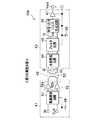
図1は、本発明の実施形態に係る半導体駆動装置10を用いた電力変換装置100の構成を示す図である。
電力変換装置100は、半導体駆動装置10と、半導体駆動装置10の出力によりゲート電圧が制御されるIGBT(Insulated Gate Bipolar Transistor:絶縁ゲートハイポーラトランジスタ)の半導体スイッチング素子Q1と、負荷4と、電源5とを備えている。<< First Embodiment >>
Hereinafter, a semiconductor drive device and a power conversion device according to a first embodiment of the present invention will be described in detail with reference to the drawings.
FIG. 1 is a diagram showing a configuration of a
The
半導体駆動装置10は、指令信号が入力される駆動指令INを入力とする指令信号駆動部1と、指令信号駆動部1の出力を入力とする絶縁通信部2と、絶縁通信部2の出力を入力とする出力部3とを備える。
指令信号駆動部1は、連続パルス生成部6と駆動部7とを備える。
出力部3は、判定部8と出力パルス生成部9とを備える。The
The command
The output unit 3 includes a
次に、このような構成において動作を説明する。
図2は、半導体駆動装置10を構成する各点における電圧波形を示す図である。
指令信号駆動部1は、連続パルス生成部6が駆動指令INのオン期間(図2に示す指令信号のオン:以下、指令信号オンと表記する)に応じた所定周期の連続するパルス電圧Vaを生成し(図1に示すA点、図2参照)、駆動部7がパルス電圧Vaに応じて絶縁通信部2にパルス電圧を印加する。Next, the operation in such a configuration will be described.
FIG. 2 is a diagram illustrating a voltage waveform at each point constituting the
The command
この絶縁通信部2は絶縁型のトランス(パルストランス)が用いられ、該絶縁トランスの送信側(入力側)端子間に駆動部7からのパルス電圧が印加される。
出力部3においては、判定部8が絶縁通信部2の該絶縁トランスの受信側(出力側)端子間のパルス電圧に応じたパルス電圧Vbを出力し(図1に示すB点、図2参照)、出力パルス生成部9が入力されるパルス電圧Vbに基づいてパルス電圧Vaの周期よりも長い一定幅の駆動電圧Voutを1パルス出力する。この駆動電圧Voutは、半導体スイッチング素子Q1のゲートをオンにする。さらに複数のパルス電圧Vbが入力された場合、出力部3は、複数のパルス電圧Vbに基づいて駆動電圧Voutのパルス幅を加算する。The insulating communication unit 2 uses an insulating transformer (pulse transformer), and a pulse voltage from the
In the output unit 3, the
このような構成により、連続パルス生成部6から所定周期のパルス電圧Vaが出力される期間、出力パルス生成部9から半導体スイッチング素子Q1のゲートをオンにする駆動電圧(Vout)が出力される(図2参照)。
前記したように半導体駆動装置10は、駆動指令INに指令信号オンが入力された期間に応じて半導体スイッチング素子Q1のゲートをオンにする。With such a configuration, the drive voltage (Vout) for turning on the gate of the semiconductor switching element Q1 is output from the
As described above, the
図1に示す電力変換装置100の場合、半導体スイッチング素子Q1がオンされるとオン指令出力側GND21の電位は、駆動指令側GND20に対して電源5の電圧VBの電圧程度まで上昇する。この電位差は絶縁通信部2に印加される。ここで、電力変換装置100の制御の精度を向上させるには、半導体スイッチング素子Q1のゲートをオンにする電圧のパルス幅の精度を高くすること、すなわち、駆動指令INと駆動電圧Voutのパルス幅がよく一致していることが必要である。そのためには、出力パルス生成部9で1パルス出力するパルス幅を短くすることと、時間当たりのパルスの数を多くすることが望ましい。 In the case of the
また、電力変換装置100において、実際の設計では十分にノイズマージンを持たせて設計するが、仮に想定外のノイズが装置の回路に進入した場合でも、ノイズ発生期間に応じた半導体スイッチング素子Q1のゲートオン電圧が生じるものの、従来のラッチ回路を用いた場合のように誤作動を保持しないため、短時間だけゲートオンするもののノイズの消滅により正常動作への復旧が可能である。 In the
さらに、半導体スイッチング素子Q1のゲートは、入力容量を持って低域通過フィルタとしても機能するため、出力パルス生成部9の1パルス出力時のパルス幅を十分短く設定すれば、半導体スイッチング素子Q1のゲート電圧(駆動電圧Vout)のしきい電圧まで上昇せず誤ってゲートがオンになることを防いでいる。
また、電力変換装置100は、半導体駆動装置10の駆動指令INから絶縁通信部2までの回路内で配線が断線するといった不具合が生じた場合でも、絶縁通信部2の受信側(出力側)にパルス電圧が生じないので、半導体スイッチング素子Q1のゲートがオフ状態を保持して回路内で不具合を生じさせないようにしている。Further, since the gate of the semiconductor switching element Q1 has an input capacitance and also functions as a low-pass filter, if the pulse width at the time of outputting one pulse of the
In addition, the
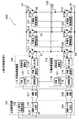
図3は、半導体駆動装置10の具体的な構成例を示す図である。なお、図1に示した半導体駆動装置10と同一箇所には同一符号を付して説明を省略する。
連続パルス生成部6Aは、アンド回路22で構成され、内部もしくは外部から供給される指令信号(IN)とクロック信号(CLK)の論理積をとり連続パルスを生成する。以下、内部から供給されるものとして説明する。FIG. 3 is a diagram illustrating a specific configuration example of the
The
駆動部7は、立上りエッジパルス発生回路24と立下りエッジパルス発生回路25とを有するエッジトリガパルス発生回路15,ドライバコントローラ17,ドライバ26とドライバ27とを有する駆動回路19を備える。
絶縁通信部2は、絶縁型のパルストランスである絶縁トランス12で構成される。
判定部8は、受信抵抗28,29と、コンパレータ30,31と、ナンド回路32とを備える。The
The insulating communication unit 2 includes an insulating
The
出力パルス生成部9は、エッジトリガパルス発生回路34,ドライバ35を備える。
なお、絶縁通信部2を構成する絶縁トランス12の指令信号駆動部1に接続される巻き線側(図3上の左側)が駆動指令側(送信側)となり、絶縁トランス12の出力部3に接続される巻き線側(図3上の右側)がオン指令出力側(受信側)となる。The output
The winding side (left side in FIG. 3) connected to the command
次に、このような構成において動作を説明する。
図4は、図3に示す半導体駆動装置10を構成する各点における電圧波形を示す図である。
図3において、連続パルス生成部6Aは、内部から駆動指令(IN)に供給する指令信号オンと、内部から供給する周期tckのクロック信号(CLK)との論理積をアンド回路22でとって連続パルス(IN×CLK)を生成する(図4参照)。Next, the operation in such a configuration will be described.
FIG. 4 is a diagram showing voltage waveforms at points constituting the
In FIG. 3, the
駆動部7は、アンド回路22で生成された連続パルス(IN×CLK)を入力とする。また、アンド回路22には、駆動指令側GND20が接続される。駆動部7は、エッジトリガパルス発生回路15において、立上りエッジパルス発生回路24が入力される連続パルス(IN×CLK)の立上りエッジから所定の幅tpのパルス電圧(D点:図4参照)を生成し、立下りエッジパルス発生回路25が入力される連続パルス(IN×CLK)の立下りエッジから所定の幅tpのパルス電圧(E点:図4参照)を生成する。パルス電圧(D点)は、図3に示す立上りエッジパルス発生回路24のD点の出力を示し、パルス電圧(E点)は、図3に示す立下りエッジパルス発生回路25のE点の出力を示す。また、立上りエッジパルス発生回路24,立下りエッジパルス発生回路25には、駆動指令側GND20が接続される。 The
続いて駆動部7は、駆動回路19において、ドライバ26が立上りエッジパルス発生回路24で生成した所定幅tpのパルス電圧(D点)を絶縁トランス12の駆動指令側の巻き線の一方の端子に印加し、ドライバ27が立下りエッジパルス発生回路25で生成した所定幅tpのパルス電圧(E点)を絶縁トランス12の駆動指令側の巻き線の他方の端子に印加する。また、ドライバ26,ドライバ27には、駆動指令側GND20が接続される。 Subsequently, in the
なお、駆動部7のドライバコントローラ17は、駆動回路19がパルス電圧を送信しない期間に、パルス電圧を送信する期間に比べ駆動回路19の出力段をハイインピーダンスとする指令を出す。具体的にドライバコントローラ17は、駆動回路19でパルス電圧を送信しない期間、駆動回路19が有するドライバ26,27の出力段をオフにする。
この結果、図3に示すように、絶縁トランス12の駆動指令側(送信側)の端子間に電圧Vsが印加され、絶縁トランス12のオン指令出力側(受信側)の端子間に電圧Vtが出力される。このときの端子間電圧Vsと端子間電圧Vtを図4に示す。Note that the driver controller 17 of the
As a result, as shown in FIG. 3, the voltage Vs is applied between the drive command side (transmission side) terminals of the
出力部3の判定部8には、絶縁トランス12のオン指令出力側の巻き線の端子間電圧Vtが入力される。
判定部8において、絶縁トランス12のオン指令出力側の巻き線の端子間に受信抵抗28,29が直列に接続され、受信抵抗28と受信抵抗29との間にオン指令出力側GND21が接続される。The inter-terminal voltage Vt of the winding on the ON command output side of the
In the
コンパレータ30,31は、絶縁トランス12のオン指令出力部側の巻き線の端子間に接続される。その際、コンパレータ30の−入力端子と+入力端子と、コンパレータ31の−入力端子と+入力端子とが、絶縁トランス12の端子間に互いに異なるようにそれぞれ接続され、絶縁トランス12の端子間電圧Vtの正、負を判定する。また、コンパレータ30,31には、オン指令出力側GND21が接続される。
ナンド回路32は、コンパレータ30の出力とコンパレータ31の出力とを入力とし、クロック信号(CLK)と駆動指令(IN)に入力された指令信号オンの論理積(IN×CLK:図4参照)のエッジに対応した連続パルス電圧(図4参照)を出力する(図3のF点)。また、ナンド回路32には、オン指令出力側GND21が接続される。The
The
出力パルス生成部9において、エッジトリガパルス発生回路34は、連続パルス電圧(F点)の入力に対し、クロック信号(CLK)の周期tckの1/2より長いパルス幅twのエッジトリガのパルスを発生する。ドライバ35は、エッジトリガパルス発生回路34からのパルス幅twのパルスに応じて駆動電圧Voutを出力する(図4参照)。また、ドライバ35には、オン指令出力側GND21が接続される。
このように、エッジトリガパルス回路34が再トリガすることで、パルス幅twのパルス電圧が連続して発生する期間では、半導体スイッチング素子Q1のゲートをなめらかにオンにする駆動電圧Voutが出力される(図4参照)。In the output
As described above, when the edge
この第1の実施形態によれば、駆動部7が立上りエッジと立下りエッジからパルス電圧を生成することにより、つまり、図4のVs,Vtに示すようにパルス電圧の極性を交互に変えることで電流の向きが変わり、これにより絶縁トランス12がリセットされ、磁気飽和を避けることができる。さらに、出力パルス生成部9は、パルス幅twをクロック信号CLKの周期tckの1/2近くまで短くできるので、半導体スイッチング素子Q1のゲートをオンにするパルス電圧(駆動電圧)のパルス幅の精度を高めることが可能となる。 According to the first embodiment, the
さらに、絶縁トランス12の端子間電圧Vtの正、負を判定する判定部8を用いることで、図3に示すトランスの寄生容量(C1,C2)に起因する同相ノイズの除去が可能となる。これは、前記した図1の電力変換装置100で半導体スイッチング素子Q1をオン、オフした際に発生するオン指令出力側GND21と駆動指令側GND20との間の電位差Vhの電圧変化dVh/dtによる変移電流と、受信抵抗28の積のC1×(dVh/dt)×R(受信抵抗28)のノイズと、受信抵抗29の積のC2×(dVh/dt)×R(受信抵抗29)のノイズとが同相モードで判定部8に入力されるが、差動判定することで同相のノイズが除去されるためである。この結果、ノイズ耐量を向上させることができる。 Furthermore, by using the
図5は、ノイズ耐量をさらに向上させた判定部8Aの構成例を示す図である。図3に示した判定部8と同一箇所には同一符号を付して説明を省略する。判定部8Aは、絶縁トランス12の受信側の両端子とコンパレータ(30,31)の入力端子との間に電圧調整回路201,202,203,204を設けたものである。
電圧調整回路201は、入力側が受信抵抗28の一端が接続されている絶縁トランス12の端子に接続され、出力側がコンパレータ30の−入力端子に接続されている。
電圧調整回路202は、入力側が受信抵抗29の一端が接続されている絶縁トランス12の端子に接続され、出力側がコンパレータ30の+入力端子に接続されている。FIG. 5 is a diagram illustrating a configuration example of the
The
The
電圧調整回路203は、入力側が受信抵抗29の一端が接続されている絶縁トランス12の端子に接続され、出力側がコンパレータ31の−入力端子に接続されている。
電圧調整回路204は、入力側が受信抵抗28の一端が接続されている絶縁トランス12の端子に接続され、出力側がコンパレータ31の+入力端子に接続されている。
電圧調整回路201,203は、コンパレータ30,31の+入力端子の判定における基準電圧レベルを調整する回路である。The
The
The
図6は、電圧調整回路201,203の回路構成を示すもので、ダイオード211,抵抗(Rad1)213,抵抗(Rad2)214を備える。入力電圧はダイオード211により直流電圧Vdcとなる。この直流電圧Vdcを抵抗分圧した電圧Vad0=Rad2/(Rad1+Rad2)×Vdcとなるまで出力電圧はVad0となり、これが基準レベルとなる(基準信号)。入力電圧がさらに上昇すると、この電圧上昇にほぼ比例して判定の基準レベルが上昇する。 FIG. 6 shows a circuit configuration of the
図7は、電圧調整回路202,204の回路構成を示すもので、ダイオード215,抵抗(Rad3)216,抵抗(Rad4)217を備える。電圧調整回路202,204が備える抵抗216,217は、図6に示す電圧調整回路201,203が備える抵抗と抵抗値が異なるものである。
電圧調整回路202,204は、コンパレータ30,31の−入力端子に印加される判定すべき電圧信号(判定信号)のレベルを調整する。FIG. 7 shows a circuit configuration of the
The
図5に示す判定部8Aのコンパレータ30,31の−入力端子側が+入力端子側より高い電圧となり、出力が「ロー」となった場合に、そのエッジから連続のパルス電圧を生成する場合を想定すると、電圧調整回路202,204は、直流電圧Vhgを抵抗分圧した出力電圧Vehが電圧調整回路201,203の出力電圧Vadより低く設定される。
すなわち、絶縁トランス12の一方の出力端子に接続される基準レベルの電圧を調整する電圧調整回路(第1の基準電圧調整回路)201の出力電圧(基準電圧)Vehは、判定レベルの電圧を調整する電圧調整回路(第2の判定電圧調整回路)202の出力電圧(判定電圧)Vadより低く設定され、絶縁トランス12の他方の出力端子に接続される基準レベルの電圧を調整する電圧調整回路(第2の基準電圧調整回路)203の出力電圧(基準電圧)Vehは、判定レベルの電圧を調整する電圧調整回路(第1の判定電圧調整回路)204の出力電圧(判定電圧)Vadより低く設定される。Assuming a case where a continuous pulse voltage is generated from the edge when the −input terminal side of the
That is, the output voltage (reference voltage) Veh of the voltage adjustment circuit (first reference voltage adjustment circuit) 201 that adjusts the reference level voltage connected to one output terminal of the
このような構成により、電圧調整回路(201,202,203,204)の基準信号側の入力と判定信号側の入力に同一の電圧が印加された場合、必ず、判定信号側の電圧調整回路(202,204)の出力電圧を低くできる。このため、絶縁トランス12における入力端子と出力端子との間の寄生容量の差(C1、C2)、さらに受信抵抗28,29のばらつきにより判定部8Aの平衡性が失われて同相ノイズが差動ノイズに変換された場合でも、判定信号側の電圧調整回路(202,204)の出力電圧を低くすることでノイズによる誤動作を回避することが可能となる。 With such a configuration, when the same voltage is applied to the reference signal side input and the determination signal side input of the voltage adjustment circuit (201, 202, 203, 204), the determination signal side voltage adjustment circuit ( 202, 204) can be lowered. For this reason, the balance of the
≪第2の実施形態≫
次に、第2の実施形態に係る半導体駆動装置と電力変換装置について説明する。
図8は、本発明の第2の実施形態に係る半導体駆動装置10aと、半導体駆動装置10aを用いた電力変換装置100aの構成を示す図である。なお、図3に示した半導体駆動装置10と同一箇所には同一符号を付して説明を省略する。また、図1に示した電力変換装置100と同一箇所には同一符号を付して説明を省略する。<< Second Embodiment >>
Next, a semiconductor drive device and a power conversion device according to the second embodiment will be described.
FIG. 8 is a diagram showing a configuration of a
半導体駆動装置10aは、図3に示した半導体駆動装置10に状態信号駆動部67,状態出力部66,受信対応駆動指令部73,送信対応受信信号処理部76を設けたものである。状態信号駆動部67は半導体スイッチング素子Q1のオン状態を判定して状態信号を送信するものであり、その送信された状態信号を受信して半導体スイッチング素子Q1のオン状態のオン状態検知信号を出力するものが状態出力部66である。すなわち、半導体駆動装置10aと電力変換装置100aは、駆動指令INからの指令信号オンの送信と、半導体スイッチング素子Q1の状態信号の送信とを絶縁トランス12を介して双方向に通信する構成である。
なお、半導体駆動装置10aは、マイクロコンピュータなどの上位機器(図示しない)から駆動指令INに指令信号オンが入力される構成となっている。The
The
指令信号駆動部1Aは、連続パルス生成部6,エッジトリガパルス発生回路15と駆動回路19とを備える駆動部7,受信対応駆動指令部73を備える。
出力部3Aは、判定部8,出力パルス生成部9,送信対応受信信号処理部76を備える。
状態出力部66は、出力パルス生成部78,送信対応受信信号処理部79,判定部80を備える。判定部80は、絶縁通信部2の絶縁トランス12の入力側(送信側)の端子を入力とする。The command signal drive unit 1A includes a continuous
The output unit 3A includes a
The
状態信号駆動部67は、駆動回路81aとエッジトリガパルス発生回路81bとを備える駆動部82,連続パルス生成部83,状態判定部84,受信対応駆動指令部85を備える。状態判定部84は、半導体スイッチング素子Q1のゲート−エミッタ間の電圧を入力とする。駆動回路81aの出力は、絶縁通信部2の絶縁トランス12の出力側(受信側)の端子に入力される。 The state
次に、このような構成において動作を説明する。
図9は、半導体駆動装置10aを構成する各点における電圧波形を示す図である。
まず、状態信号駆動部67において、状態判定部84が半導体スイッチング素子Q1のゲートがオンであると判定した際、連続パルス生成部83,エッジトリガパルス発生回路81bを介して駆動回路81aが連続パルス(第2の連続パルス)を絶縁通信部2の絶縁トランス12の出力側に出力(送信)する。Next, the operation in such a configuration will be described.
FIG. 9 is a diagram showing voltage waveforms at each point constituting the
First, in the state
状態出力部66において、判定部80が前記送信された連続パルスを絶縁トランス12の入力側で受信し、出力パルス生成部78が1つのパルスに対してパルス幅twのパルスを再トリガして発生し、半導体スイッチング素子Q1がオン状態であるとするオン状態検知信号を入力端子STATEを介して上位機器(図示しない)へ出力する。
上位機器(図示しない)は、オン状態検知信号が入力端子STATEに入力されることにより、半導体スイッチング素子Q1のオン,オフ状態を検知することができる。In the
The host device (not shown) can detect the on / off state of the semiconductor switching element Q1 by inputting the on state detection signal to the input terminal STATE.
また、状態信号駆動部67の受信対応駆動指令部85は、駆動回路81aがパルスを送信しない期間に、パルスを送信する期間に比べ駆動回路81aの出力段をハイインピーダンスとする指令を出す。具体的に受信対応駆動指令部85は、駆動回路81aがパルスを送信しない期間、駆動回路81aの出力段をオフにする。 In addition, the reception-compatible
同様に、指令信号駆動部1Aの受信対応駆動指令部73は、駆動回路19がパルス電圧を送信しない期間に、パルス電圧を送信する期間に比べ駆動回路19の出力段をハイインピーダンスとする指令を出す。具体的に受信対応駆動指令部73は、駆動回路19がパルスを送信しない期間、駆動回路19の出力段をオフにする。この場合、指令信号駆動部1Aにおける駆動回路19の出力インピーダンスは、パルス電圧を送信しない期間は判定部8の受信抵抗(図3に示す受信抵抗28,29)Rとなるが、パルス電圧(D点、E点)を送信する期間は並列に駆動回路19の出力段の抵抗RDが入るため抵抗の値が下がる(図8と図9を参照)。 Similarly, the reception-compatible
このような構成により、絶縁通信部2が半導体スイッチング素子Q1のゲートをオン状態とする連続するパルス電圧を受信するとき受信側の等価的なインピーダンスが高くなり、より少ない駆動回路19からの電流で送信を可能とし、駆動回路19の小型化と低損失化を図ることができる。 With this configuration, when the insulating communication unit 2 receives a continuous pulse voltage that turns on the gate of the semiconductor switching element Q1, the equivalent impedance on the receiving side is increased, and less current from the
状態信号駆動部67からのパルス(半導体スイッチング素子Q1のゲートをオン状態と判定した状態信号P)の送信は、絶縁トランス12の出力側の端子間電圧Vtに示すように、指令信号(半導体スイッチング素子Q1のゲートをオン状態にする送信信号S)に同期し、時間tdだけ遅れて出力することで指令信号と重ならないようにしている。また、送信信号Sが発生していない期間は、同期する信号が無いため、状態信号駆動部67の連続パルス生成部83で生成するクロック信号(tck2)の周波数でパルス(状態信号P)を送信する(図9参照)。なお、指令信号駆動部61の連続パルス生成部6は、クロック信号(tck1)の周波数でパルスを生成して送信する(図9参照)。 Transmission of a pulse from the state signal driving unit 67 (state signal P determined that the gate of the semiconductor switching element Q1 is turned on) is a command signal (semiconductor switching) as indicated by the inter-terminal voltage Vt on the output side of the
また、半導体スイッチング素子Q1から出力されるオン状態検知信号(図9参照)において、tdonは半導体スイッチング素子Q1のゲートのターンオンの遅延時間であり、tdoffは半導体スイッチング素子Q1のゲートのターンオフの遅延時間である。
状態出力部66においては、判定部80が絶縁トランス12の送信側(入力側)端子間のパルス電圧Vsに応じたパルス電圧を受信し、出力パルス生成部78が入力されるパルス電圧に基づいてクロック信号(CLK)の周期tck1(tck2)の1/2より長いパルス幅twのエッジトリガのオン状態検知信号を入力端子STATEを介して上位機器(図示しない)に1パルス出力する。In the ON state detection signal (see FIG. 9) output from the semiconductor switching element Q1, tdon is a delay time for turning on the gate of the semiconductor switching element Q1, and tdoff is a delay time for turning off the gate of the semiconductor switching element Q1. It is.
In the
出力部3Aの送信対応受信信号処理部76は、駆動回路81aのパルス送信期間に信号をマスクして受信しない期間とする。このような構成により、出力部3Aは、状態信号を受信信号と誤判定せず信頼性の高い信号の伝送が可能となる。
同様に、状態出力部66の送信対応受信信号処理部79は、駆動回路19のパルス送信期間に信号をマスクして受信しない期間とする。このような構成により、状態出力部66は、状態信号と指令信号とを誤判定せず信頼性の高い信号の伝送が可能となる。The transmission corresponding received
Similarly, the transmission corresponding received
なお、連続パルス生成部6で生成される連続パルスを第1の連続パルスとした場合、連続パルス生成部83で生成される連続パルスは第2の連続パルスとなる。
この第2の実施形態によれば、上位機器(図示しない)から供給される指令信号オンの送信と、半導体スイッチング素子Q1のオン状態検知信号の送信とを絶縁トランスを介して双方向に通信する構成により、該上位機器(図示しない)は、供給した指令信号オンに応じて制御されるスイッチング素子Q1のオン、オフ状態を検知することができる。When the continuous pulse generated by the
According to the second embodiment, the transmission of the command signal ON supplied from the host device (not shown) and the transmission of the ON state detection signal of the semiconductor switching element Q1 are bidirectionally communicated via the insulating transformer. According to the configuration, the host device (not shown) can detect the on / off state of the switching element Q1 that is controlled in response to the supplied command signal being on.
≪第3の実施形態≫
次に、第3の実施形態に係る半導体駆動装置について説明する。
図10は、全波整流回路44を用いた半導体駆動装置10bの構成例を示す図である。図11は、半導体駆動装置10bを構成する各点における電圧波形を示す図である。
半導体駆動装置10bは、基本構成は変わらず、指令信号駆動部41,絶縁通信部42,出力部43を備えている。本構成例では、出力部43に、判定部に代わる全波整流回路44を設けている。<< Third Embodiment >>
Next, a semiconductor drive device according to a third embodiment will be described.
FIG. 10 is a diagram illustrating a configuration example of the
The
指令信号駆動部41は、駆動論理回路51と駆動回路52を備える。
絶縁通信部42は、絶縁トランス53で構成される。
出力部43は、全波整流回路44,フィルタ回路45,判定・出力パルス生成回路46,ドライバ47を備える。
本構成例の半導体駆動装置10bにおいては、指令信号オンの時、駆動論理回路51と駆動回路52を備える指令信号駆動部41から送信される連続のパルス電圧が絶縁トランス53の入力側端子間に印加され、絶縁トランス53の出力側端子間(図10のG点)に差電圧Vcが出力(生成)される(図11参照)。The command
The insulating
The
In the
出力部43は、全波整流回路44で差電圧Vcを整流し、整流した電圧がある一定以上の値の期間、半導体スイッチング素子のゲートをオンとする指令を出力(駆動電圧Vout)する。なお、フィルタ回路45は、全波整流回路44で整流した際のノイズを除くために設けられている。 The
前記第3の実施形態によれば、半導体駆動装置10bでは、絶縁トランス53の出力側端子の差電圧Vcを全波整流回路44で整流しているので差動の電圧Vd(図10のH点)が容易に得られ(図11参照)、判定・出力パルス生成回路46を簡素化できる。
また、指令信号駆動部41からの送信信号を連続の矩形波で送信すれば、フィルタ回路45の出力(差動の電圧)Vdの電圧レベルが高い場合(所定のしきい値レベル)に半導体スイッチング素子Q1のゲートをオンとする出力にすればよく、判定・出力パルス生成回路46を簡素化することができる。According to the third embodiment, in the
Further, if the transmission signal from the command
なお、図11に示したクロック信号(CLK)は、差電圧Vcと差動の電圧Vdの関係を説明するため図示を簡素化しているもので、図4、図9で示したクロック信号(CLK)と同様の周期tckである。 The clock signal (CLK) shown in FIG. 11 is simplified to illustrate the relationship between the differential voltage Vc and the differential voltage Vd. The clock signal (CLK) shown in FIGS. ) And the same period tck.
図12は、絶縁通信部2Aの他の構成例を示す図である。絶縁通信部2Aは、2つの絶縁トランス92,94が直列に接続される。絶縁トランス92と絶縁トランス94とが直列接続されている接続点の絶縁トランス92側にコンデンサ98を介してGND96が接続され、接続点の絶縁トランス94側にコンデンサ99を介してGND97が接続されている。GND96とGND97の間に電圧差が生じた場合に、絶縁トランス92の寄生容量93と絶縁トランス94の寄生容量95とにアンバランスが生じてもコンデンサ98,99が接続されているので印加される電圧が均等に分担される。 FIG. 12 is a diagram illustrating another configuration example of the
このような構成により、絶縁トランスを直列に接続しても各絶縁トランスに印加する電圧を低く抑えることができ、小型化した絶縁通信部を構成することができる。ここで、コンデンサ98,99は、容量が小さいことが耐ノイズ性から望ましく、寄生容量93,95のアンバランスを調整できれば良いため、たとえば、プリント基板での配線の寄生Cなどを用いることも可能である。その結果、半導体駆動装置の小型化も可能である。 With such a configuration, even if the insulating transformers are connected in series, the voltage applied to each insulating transformer can be kept low, and a miniaturized insulating communication unit can be configured. Here, it is desirable that the
≪第4の実施形態≫
第4の実施形態では、図8に示した半導体駆動装置10aを複数用いた場合における電力変換装置の応用例について説明する。
図13は、半導体駆動装置109,114,119,120,121,122を用いた電力変換装置200の構成例を示す図である。半導体駆動装置109,114,119,120,121,122のそれぞれが、半導体駆動装置10aに該当する。
本応用例は、上位論理回路101からの指令を受ける半導体スイッチング素子Q11,Q12,Q13,Q14,Q15,Q16を駆動する半導体駆動装置109,114,119,120,121,122を備え、負荷であるモータ123を駆動する三相インバータ型の電力変換装置200である。<< Fourth Embodiment >>
In the fourth embodiment, an application example of the power conversion device when a plurality of
FIG. 13 is a diagram illustrating a configuration example of the
This application example includes
上位論理回路101は、例えば、マイクロコンピュータを用いて構成され、オン指令演算回路102と連続パルス生成部103,104とを備えている。オン指令演算回路102は、半導体スイッチング素子(Q11,Q12,Q13,Q14,Q15,Q16)のオン、オフの指令信号(IN)と、クロック信号(CLK)とを連続パルス生成部103,104に供給する。なお、半導体スイッチング素子のゲートをオンとする指令信号(IN)のことを指令信号オン(IN)と表記する。 The high-
連続パルス生成部103は、オン指令演算回路102から供給されるクロック信号(CLK)と指令信号オン(IN)に基づいて連続パルスを生成し、該連続パルスを保護回路107を介して半導体駆動装置109に供給する。
連続パルス生成部104は、オン指令演算回路102から供給されるクロック信号と(CLK)と指令信号オン(IN)に基づいて連続パルスを生成し、該連続パルスを保護回路106を介して半導体駆動装置114に供給する。The
The continuous
また、上位論理回路101は、半導体駆動装置119,120,121,122のそれぞれに対応する連続パルス生成部(図示しない)を備え、それぞれの連続パルス生成部(図示しない)が保護回路(図示しない)を介して各半導体駆動装置(119,120,121,122)に接続されている。 The higher-
前記したように、半導体駆動装置109,114,119,120,121,122へ供給される指令信号オン(IN)に基づく連続パルスは、すべて同一のクロック信号(CLK)に同期して出力される。
なお、図13では、直列接続されて上下アームを構成する半導体スイッチング素子Q11,Q12を駆動する半導体駆動装置109,114の回路構成を示し、同様の回路構成を備える半導体駆動装置119,120と半導体駆動装置121,122について図示を省略している。As described above, continuous pulses based on the command signal ON (IN) supplied to the
FIG. 13 shows the circuit configuration of the
半導体駆動装置109は、駆動部110,絶縁通信部111,出力部112,状態出力部113,状態信号駆動部130を備える。半導体駆動装置109と図8に示す半導体駆動装置10aとを対比すると、駆動部110が駆動部7に相当し、絶縁通信部111が絶縁通信部2に相当し、出力部112が出力部3Aに相当し、状態出力部113が状態出力部66に相当し、状態信号駆動部130が状態信号駆動部67に相当する。 The
駆動部110は、保護回路107を介して供給される連続パルスに応じて絶縁通信部111にパルス電圧を印加する。絶縁通信部111は、絶縁トランスで構成され、該絶縁トランスの送信側(入力側)端子間に駆動部110からのパルス電圧が印加され、該絶縁トランスの受信側(出力側)端子間でパルス電圧が出力部112に出力される。 The driving
出力部112は、入力されるパルス電圧に基づいて一定幅の駆動電圧を半導体スイッチング素子Q11のゲートに出力する。この駆動電圧は、半導体スイッチング素子Q11のゲートをオンにする。
状態信号駆動部130は、半導体スイッチング素子Q11のオン状態を判定して状態信号を絶縁通信部111の受信側に送信する。
状態出力部113は、絶縁通信部111の送信側で受信される状態信号を半導体駆動装置114の駆動部115に出力する。The
The state
The state output unit 113 outputs a state signal received on the transmission side of the
半導体駆動装置114は、駆動部115に状態信号が入力されることにより、半導体スイッチング素子Q11のオン,オフ状態を検知することができる。
一方、半導体駆動装置114は、駆動部115,絶縁通信部116,出力部117,状態出力部118,状態信号駆動部131を備える。半導体駆動装置114と図8に示す半導体駆動装置10aとを対比すると、駆動部115が駆動部7に相当し、絶縁通信部116が絶縁通信部2に相当し、出力部117が出力部3Aに相当し、状態出力部118が状態出力部66に相当し、状態信号駆動部131が状態信号駆動部67に相当する。The
On the other hand, the
駆動部115は、保護回路106を介して供給される連続パルスに応じて絶縁通信部116にパルス電圧を印加する。絶縁通信部116は、絶縁トランスで構成され、該絶縁トランスの送信側(入力側)端子間に駆動部115からのパルス電圧が印加され、該絶縁トランスの受信側(出力側)端子間でパルス電圧が出力部117に出力される。 The driving
出力部117は、入力されるパルス電圧に基づいて一定幅の駆動電圧を半導体スイッチング素子Q12のゲートに出力する。この駆動電圧は、半導体スイッチング素子Q12のゲートをオンにする。
状態信号駆動部131は、半導体スイッチング素子Q12のオン状態を判定して状態信号を絶縁通信部116の受信側に送信する。
状態出力部118は、絶縁通信部116の送信側で受信される状態信号を半導体駆動装置109の駆動部110に出力する。
半導体駆動装置109は、駆動部110に状態信号が入力されることにより、半導体スイッチング素子Q12のオン,オフ状態を検知することができる。The
The
The state output unit 118 outputs a state signal received on the transmission side of the insulating
The
前記したように、半導体スイッチング素子Q11のオン、オフの状態が、半導体スイッチング素子Q11を駆動する半導体駆動装置109の状態信号駆動部130,絶縁通信部111,状態出力部113を経由して半導体スイッチング素子Q12の半導体駆動装置114の駆動部115に伝送される。
同様に、半導体スイッチング素子Q12のオン、オフの状態が、半導体スイッチング素子Q12を駆動する半導体駆動装置114の状態信号駆動部131,絶縁通信部116,状態出力部118を経由して半導体スイッチング素子Q11の半導体駆動装置109の駆動部110に伝送される。As described above, the semiconductor switching element Q11 is turned on and off via the state
Similarly, the semiconductor switching element Q12 is turned on and off via the state
このような構成により、インバータ(半導体駆動装置109,114)の対となる上下のアーム間で、双方向通信により受信した対アームの半導体スイッチング素子(Q11,Q12)のオン、オフの状態を共有し、対アームがオンの時には自アームをオンしないように制御される。
そして、半導体駆動装置119,120と半導体駆動装置121,122とが、前記した半導体駆動装置109,114と同様に対アームとして制御される。With such a configuration, the on / off states of the paired semiconductor switching elements (Q11, Q12) received by bidirectional communication are shared between the upper and lower arms that form a pair of the inverters (
Then, the
なお、本応用例では、上位論理回路101と各半導体駆動装置(109,114,119,120,121,122)との間に、保護回路106,107,及び図示しない保護回路を設けている。保護回路106,107,及び図示しない保護回路は、サージ吸収回路,ヒューズ等で構成され、各半導体駆動装置の絶縁通信部や他の部分で放電等が生じた場合を想定し、このときに発生する過電流や過電圧によって上位論理回路101に破壊が生じないようにしている。 In this application example,
この第4の実施形態によれば、電力変換装置200は、ノイズ等により誤まった指令が発生しても、対アームの半導体スイッチング素子の同時オンによる不具合を回避でき、信頼性の高い制御を可能とする。
また、電力変換装置200は、指令信号と連続パルス信号とが同期するので、半導体スイッチング素子のゲートのオン期間の時間精度が高く、より高精度な制御を可能とする。According to the fourth embodiment, the
In addition, since the command signal and the continuous pulse signal are synchronized with each other, the
さらに、電力変換装置200は、オン期間の時間精度を高めるために上位論理回路101からのクロック信号に各半導体駆動装置間の連続パルスを同期させるようにしても良く、各半導体駆動装置間のパルス出力を同期させるようにしても良い。
また、保護回路を用いることにより、電力変換装置200を、より高精度で信頼性の高い装置にすることができる。
前記した半導体駆動装置、電力変換装置を用いることにより、例えば、高速鉄道などの交通手段、風力発電などの発電設備で、小型、高精度、さらに信頼性の高い機器を提供することができる。Further, the
Further, by using the protection circuit, the
By using the semiconductor drive device and the power conversion device described above, it is possible to provide a small, highly accurate, and highly reliable device using, for example, transportation means such as a high-speed railway and power generation facilities such as wind power generation.
1,41,61 指令信号駆動部
2,42 絶縁通信部
3,43,63 出力部
4 負荷
5 電源
6 連続パルス生成部
7 駆動部
8 判定部
9 出力パルス生成部
10,10a,10b 半導体駆動装置
12,53 絶縁トランス
19 駆動回路
20 駆動指令側GND
21 オン指令出力側GND
24 立上りエッジパルス発生回路(第1のパルス発生回路)
25 立下りエッジパルス発生回路(第2のパルス発生回路)
66 状態出力部
67 状態信号駆動部
100,100a,200 電力変換装置
Q1,Q11,Q12,Q13,Q14,Q15,Q16 半導体スイッチング素子
92,94 絶縁トランス(第1のトランス、第2のトランス)
93,95 コンデンサ(第1のコンデンサ、第2のコンデンサ)
201,203 電圧調整回路(第1、第2の基準電圧調整回路)
202,204 電圧調整回路(第1、第2の判定電圧調整回路)DESCRIPTION OF
21 ON command output side GND
24 Rising edge pulse generation circuit (first pulse generation circuit)
25 Falling edge pulse generation circuit (second pulse generation circuit)
66
93,95 capacitor (first capacitor, second capacitor)
201, 203 Voltage adjustment circuit (first and second reference voltage adjustment circuits)
202, 204 Voltage adjustment circuit (first and second determination voltage adjustment circuits)
Claims (7)
Translated fromJapanese前記半導体駆動装置が、
前記半導体スイッチング素子のオン駆動を指令する期間中、該オン駆動を指令する、パルス間にすき間を有する連続パルスの電圧信号を生成すべく、前記連続パルスの立上りエッジに対応して所定幅のパルス電圧を出力する第1のパルス発生回路と、前記連続パルスの立下りエッジに対応して所定幅のパルス電圧を出力する第2のパルス発生回路とを具備する指令信号駆動部と、
前記指令信号駆動部で生成される連続パルスの電圧信号をトランスにより伝送する絶縁通信部と、
前記絶縁通信部を介して伝送される連続パルスの電圧信号に基づいて、前記連続パルスを構成するパルス間のすき間を埋めるように前記半導体スイッチング素子をオン駆動する駆動電圧を生成して出力する出力部と、
を備え、
前記第1のパルス発生回路から出力されるパルス電圧が前記絶縁通信部のトランスの一方の入力端子に印加され、前記第2のパルス発生回路から出力されるパルス電圧が前記絶縁通信部のトランスの他方の入力端子に印加されることを特徴とする電力変換装置。A power conversion device comprising a semiconductor switching element and a semiconductor drive device that controls driving of the semiconductor switching element on and off,
The semiconductor drive device is
A pulsehavinga predetermined width corresponding to the rising edge of the continuous pulse so as to generate a voltage signal ofa continuous pulsehaving a gap between pulses instructing the on-drive during the period in which the on-drive of the semiconductor switching element is commandedA command signal drivercomprising: a first pulse generation circuit that outputs a voltage; and a second pulse generation circuit that outputs a pulse voltage having a predetermined width corresponding to a falling edge of the continuous pulse ;
An insulating communication unit that transmits a voltage signal of a continuous pulse generated by the command signal driving unit by a transformer;
An output for generating and outputting a drive voltage for driving the semiconductor switching element to fill a gap between pulses constituting the continuous pulse based on a voltage signal of the continuous pulse transmitted through the insulation communication unit And
Equipped witha,
A pulse voltage output from the first pulse generation circuit is applied to one input terminal of the transformer of the insulation communication unit, and a pulse voltage output from the second pulse generation circuit is applied to the transformer of the insulation communication unit. A power converter, wherein the power converteris applied to the other input terminal .
前記絶縁通信部のトランスの一方の出力端子に接続され、基準レベルの電圧を調整する第1の基準電圧調整回路と、判定レベルの電圧を調整する第1の判定電圧調整回路とを備えるとともに、
前記絶縁通信部のトランスの他方の出力端子に接続され、基準レベルの電圧を調整する第2の基準電圧調整回路と、判定レベルの電圧を調整する第2の判定電圧調整回路とを備えることを特徴とする請求項2に記載の電力変換装置。The determination unit
A first reference voltage adjustment circuit that is connected to one output terminal of the transformer of the insulation communication unit and adjusts a reference level voltage; and a first determination voltage adjustment circuit that adjusts a determination level voltage;
A second reference voltage adjusting circuit for adjusting a reference level voltage, and a second determination voltage adjusting circuit for adjusting a determination level voltage, which is connected to the other output terminal of the transformer of the isolation communication unit; The power converter according to claim2 , wherein
前記第2の基準電圧調整回路と前記第1の判定電圧調整回路とに同一電圧が入力された場合に、前記第2の基準電圧調整回路から出力される基準電圧よりも前記第1の判定電圧調整回路から出力される判定電圧が低くなるように電圧調整されていることを特徴とする請求項3に記載の電力変換装置。When the same voltage is input to the first reference voltage adjustment circuit and the second determination voltage adjustment circuit, the second determination voltage is higher than the reference voltage output from the first reference voltage adjustment circuit. The voltage is adjusted so that the judgment voltage output from the adjustment circuit is low,
When the same voltage is input to the second reference voltage adjustment circuit and the first determination voltage adjustment circuit, the first determination voltage is higher than the reference voltage output from the second reference voltage adjustment circuit. 4. The power conversion device according to claim3 , wherein the voltage is adjusted so that the determination voltage output from the adjustment circuit is low.
前記半導体スイッチング素子のオン状態を検知して前記指令信号駆動部で生成される連続パルスとは異なる第2の連続パルスの電圧信号を生成し、該第2の連続パルスの電圧信号を前記絶縁通信部のトランスに印加する状態信号駆動部と、
前記絶縁通信部で伝送される前記第2の連続パルスの電圧信号に基づいて、前記第2の連続パルスを構成するパルス間のすき間を埋めるように前記半導体スイッチング素子のオン状態の検知信号を生成して出力する状態出力部と、
をさらに備えることを特徴とする請求項1に記載の電力変換装置。The semiconductor drive device is
A voltage signal of a second continuous pulse different from a continuous pulse generated by the command signal driving unit is detected by detecting an ON state of the semiconductor switching element, and the voltage signal of the second continuous pulse is generated by the insulation communication A state signal driving unit to be applied to the transformer of the unit;
Based on the voltage signal of the second continuous pulse transmitted by the insulating communication unit, a detection signal for detecting the ON state of the semiconductor switching element is generated so as to fill a gap between pulses constituting the second continuous pulse. A status output unit that outputs
The power converter according to claim1 , further comprising:
Applications Claiming Priority (1)
| Application Number | Priority Date | Filing Date | Title |
|---|---|---|---|
| PCT/JP2009/064136WO2011018835A1 (en) | 2009-08-10 | 2009-08-10 | Semiconductor drive device and power conversion device |
Publications (2)
| Publication Number | Publication Date |
|---|---|
| JPWO2011018835A1 JPWO2011018835A1 (en) | 2013-01-17 |
| JP5462880B2true JP5462880B2 (en) | 2014-04-02 |
Family
ID=43586021
Family Applications (1)
| Application Number | Title | Priority Date | Filing Date |
|---|---|---|---|
| JP2011526652AExpired - Fee RelatedJP5462880B2 (en) | 2009-08-10 | 2009-08-10 | Power converter |
Country Status (2)
| Country | Link |
|---|---|
| JP (1) | JP5462880B2 (en) |
| WO (1) | WO2011018835A1 (en) |
Cited By (1)
| Publication number | Priority date | Publication date | Assignee | Title |
|---|---|---|---|---|
| US9506809B2 (en) | 2010-11-17 | 2016-11-29 | Easytem Co., Ltd. | Portable device for measuring temperature using infrared array sensor |
Families Citing this family (5)
| Publication number | Priority date | Publication date | Assignee | Title |
|---|---|---|---|---|
| JP5753487B2 (en)* | 2011-12-28 | 2015-07-22 | 株式会社 日立パワーデバイス | COMMUNICATION SYSTEM, SEMICONDUCTOR DRIVE DEVICE, AND POWER CONVERSION DEVICE |
| JP7038511B2 (en) | 2017-09-25 | 2022-03-18 | 三菱電機株式会社 | Semiconductor integrated circuit |
| WO2024069400A1 (en)* | 2022-09-28 | 2024-04-04 | Delphi Technologies Ip Limited | Systems and methods for non-overlap enforcement for inverter for electric vehicle |
| WO2024069449A1 (en)* | 2022-09-28 | 2024-04-04 | Delphi Technologies Ip Limited | Systems and methods for non-overlap enforcement for inverter for electric vehicle |
| US12122251B2 (en) | 2022-09-28 | 2024-10-22 | BorgWarner US Technologies LLC | Systems and methods for bidirectional message architecture for inverter for electric vehicle |
Citations (3)
| Publication number | Priority date | Publication date | Assignee | Title |
|---|---|---|---|---|
| US5220204A (en)* | 1991-05-24 | 1993-06-15 | Rockwell International Corporation | Voltage and temperature compensated emitter-follower driver |
| JPH08242590A (en)* | 1995-03-01 | 1996-09-17 | Matsushita Electric Works Ltd | Drive circuit for power converting apparatus |
| JP2006074372A (en)* | 2004-09-01 | 2006-03-16 | Toshiba Corp | Digital signal transmission device |
- 2009
- 2009-08-10JPJP2011526652Apatent/JP5462880B2/ennot_activeExpired - Fee Related
- 2009-08-10WOPCT/JP2009/064136patent/WO2011018835A1/enactiveApplication Filing
Patent Citations (3)
| Publication number | Priority date | Publication date | Assignee | Title |
|---|---|---|---|---|
| US5220204A (en)* | 1991-05-24 | 1993-06-15 | Rockwell International Corporation | Voltage and temperature compensated emitter-follower driver |
| JPH08242590A (en)* | 1995-03-01 | 1996-09-17 | Matsushita Electric Works Ltd | Drive circuit for power converting apparatus |
| JP2006074372A (en)* | 2004-09-01 | 2006-03-16 | Toshiba Corp | Digital signal transmission device |
Cited By (1)
| Publication number | Priority date | Publication date | Assignee | Title |
|---|---|---|---|---|
| US9506809B2 (en) | 2010-11-17 | 2016-11-29 | Easytem Co., Ltd. | Portable device for measuring temperature using infrared array sensor |
Also Published As
| Publication number | Publication date |
|---|---|
| JPWO2011018835A1 (en) | 2013-01-17 |
| WO2011018835A1 (en) | 2011-02-17 |
Similar Documents
| Publication | Publication Date | Title |
|---|---|---|
| JP5462880B2 (en) | Power converter | |
| CN101043138B (en) | Protection circuits for semiconductor devices, protection circuits for IGBTs, and power conversion devices | |
| KR102800664B1 (en) | Low power cycle to cycle bit transfer in gate drivers | |
| JP4656263B1 (en) | Signal transmission device | |
| CN109075723B (en) | Power electronic converter and method for controlling same | |
| JP2010141990A (en) | Power conversion apparatus | |
| US10063050B2 (en) | Power supply system and power supply apparatus | |
| JP2015049104A (en) | Ac apparatus controller | |
| JP6390691B2 (en) | Signal transmission circuit | |
| JP5416673B2 (en) | Signal transmission circuit, switching element drive circuit, and power conversion device | |
| CN103580553A (en) | Movement and control system | |
| WO2017099191A1 (en) | Signal transfer circuit | |
| JP2010165116A (en) | Current detecting circuit | |
| JP2006238546A (en) | Inverter temperature detector | |
| JP6107434B2 (en) | DRIVE DEVICE AND POWER CONVERSION DEVICE | |
| JP5950084B2 (en) | Condition monitoring device | |
| JP2014233118A (en) | Inverter device | |
| JP2014011708A (en) | Bidirectional communication system, semiconductor driving device, and power conversion device | |
| JP5927060B2 (en) | Signal transmission circuit, integrated circuit, and electrical equipment including the same | |
| JP6772810B2 (en) | Power converter control system | |
| JP2014087093A (en) | Rotary electric machine for vehicle | |
| JP5050900B2 (en) | Driving device for power conversion circuit and power conversion device | |
| JPWO2018079299A1 (en) | Power converter | |
| JP6636852B2 (en) | Power converter | |
| JP5344255B2 (en) | Power converter |
Legal Events
| Date | Code | Title | Description |
|---|---|---|---|
| A131 | Notification of reasons for refusal | Free format text:JAPANESE INTERMEDIATE CODE: A131 Effective date:20130618 | |
| A521 | Request for written amendment filed | Free format text:JAPANESE INTERMEDIATE CODE: A523 Effective date:20130819 | |
| A711 | Notification of change in applicant | Free format text:JAPANESE INTERMEDIATE CODE: A712 Effective date:20131128 | |
| TRDD | Decision of grant or rejection written | ||
| A01 | Written decision to grant a patent or to grant a registration (utility model) | Free format text:JAPANESE INTERMEDIATE CODE: A01 Effective date:20140107 | |
| A61 | First payment of annual fees (during grant procedure) | Free format text:JAPANESE INTERMEDIATE CODE: A61 Effective date:20140117 | |
| R150 | Certificate of patent or registration of utility model | Free format text:JAPANESE INTERMEDIATE CODE: R150 Ref document number:5462880 Country of ref document:JP Free format text:JAPANESE INTERMEDIATE CODE: R150 | |
| S111 | Request for change of ownership or part of ownership | Free format text:JAPANESE INTERMEDIATE CODE: R313114 | |
| R350 | Written notification of registration of transfer | Free format text:JAPANESE INTERMEDIATE CODE: R350 | |
| LAPS | Cancellation because of no payment of annual fees |