JP5461205B2 - Laser processing method and apparatus - Google Patents
Laser processing method and apparatusDownload PDFInfo
- Publication number
- JP5461205B2 JP5461205B2JP2010009073AJP2010009073AJP5461205B2JP 5461205 B2JP5461205 B2JP 5461205B2JP 2010009073 AJP2010009073 AJP 2010009073AJP 2010009073 AJP2010009073 AJP 2010009073AJP 5461205 B2JP5461205 B2JP 5461205B2
- Authority
- JP
- Japan
- Prior art keywords
- substrate
- processing
- bessel beam
- laser
- irradiated
- Prior art date
- Legal status (The legal status is an assumption and is not a legal conclusion. Google has not performed a legal analysis and makes no representation as to the accuracy of the status listed.)
- Expired - Fee Related
Links
Images


Landscapes
- Laser Beam Processing (AREA)
Description
Translated fromJapanese本発明は、例えば太陽電池における周縁部の導電膜を除去するような、基板の端面部の加工を、ベッセルビームにより行う方法、及びその方法を実施する装置に関するものである。 The present invention relates to a method for processing an end surface portion of a substrate by using a Bessel beam, such as removing a conductive film at a peripheral portion of a solar cell, and an apparatus for performing the method.
従来から、液晶ディスプレイ、プラズマディスプレイ等の多くの電気製品の基板に対し、回路等のパターンが形成されている。このような回路等のパターン形成の方法としては、例えばレーザとXYテーブルスキャニングミラーを同期させる方法が用いられている。 Conventionally, patterns such as circuits are formed on substrates of many electrical products such as liquid crystal displays and plasma displays. As a pattern forming method for such a circuit, for example, a method of synchronizing a laser and an XY table scanning mirror is used.
また、これら基板上に形成された導電性薄膜の端面部の除去等においても、レーザによる加工が同様に行われている。 Further, in the removal of the end face portion of the conductive thin film formed on these substrates, processing by laser is similarly performed.
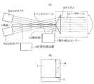
これらレーザを用いた加工として、例えば図6に示すように、円形または矩形状の加工スポット2を所定の重ね合せ率をもって移動させる方法が知られている(例えば特許文献1)。なお、図6中の1は基板、1aは基板1の端面部を示す。 As processing using these lasers, for example, as shown in FIG. 6, there is known a method of moving a circular or
しかしながら、前記レーザ加工においては、微小な円形または矩形状の加工スポットを所定の重ね合せ率をもって移動させるので、加工に時間を要し、作業効率が悪いという問題がある。特に液晶パネルや太陽電池等の大型基板になると、前記問題は顕著である。 However, in the laser processing, since a minute circular or rectangular processing spot is moved with a predetermined superposition ratio, there is a problem that processing takes time and working efficiency is poor. In particular, the problem is remarkable when a large substrate such as a liquid crystal panel or a solar cell is used.
また、加工に時間を要するので、基板にレーザを長時間照射することになるため、基板上の加工範囲以外の部分にも熱的な影響(劣化)を与えるという問題があった。 In addition, since processing takes time, the substrate is irradiated with a laser for a long time, and there is a problem in that a portion other than the processing range on the substrate is thermally affected (deteriorated).
本発明が解決しようとする問題点は、従来の微小な加工スポットを重ね合せて移動させる方法では、加工に時間を要して作業効率が悪く、また、加工に時間を要するので、基板上の加工範囲以外の部分にも熱的な影響を与えるという点である。 The problem to be solved by the present invention is that, in the conventional method of moving a small processing spot in a superimposed manner, the processing takes time and the working efficiency is poor, and the processing takes time. In other words, the thermal effect is also exerted on portions other than the processing range.
本発明のレーザ加工方法は、
レーザによる加工精度を維持しつつ加工時間を短くして、基板への熱的影響を抑制し得るようにするために、
基板にベッセルビームを照射して基板の端面部をレーザ加工する方法であって、
ベッセルビームの照射を前記基板の側面から行い、かつ、照射したベッセルビームと基板の加工位置との相対位置関係を検出しながら加工位置の補正を行いつつ、前記端面部の加工を行うことを最も主要な特徴としている。The laser processing method of the present invention comprises:
In order to shorten the processing time while maintaining the processing accuracy by the laser and to suppress the thermal influence on the substrate,
A method of laser processing an end surface portion of a substrate by irradiating a substrate with a Bessel beam,
It is most preferable to perform processing of the end face portion while performing irradiation of the Bessel beam from the side surface of the substrate and correcting the processing position while detecting the relative positional relationship between the irradiated Bessel beam and the processing position of the substrate. Main features.
前記本発明のレーザ加工方法は、
レーザビームを照射するレーザ発振器と、
このレーザ発振器より照射されたレーザビームをベッセルビームに形成する光学部材と、
基板側面から照射した、前記光学部材により形成されたベッセルビームと、基板の加工位置を検出する検出器と、
基板の傾きを検出する検出器と、
これら検出器により検出したベッセルビームと、基板の加工位置及び基板の傾きに基づき、基板、光学部材の少なくとも何れか一つの位置を制御してベッセルビームによる加工位置の補正を行う位置制御装置を備えた、本発明のレーザ加工装置を用いて実施することができる。The laser processing method of the present invention comprises:
A laser oscillator for irradiating a laser beam;
An optical member for forming a laser beam irradiated from the laser oscillator into a Bessel beam;
A Bessel beam formed by the optical member irradiated from the side surface of the substrate, a detector for detecting a processing position of the substrate,
A detector for detecting the tilt of the substrate;
Based on the Bessel beam detected by these detectors, the processing position of the substrate, and the tilt of the substrate, a position control device is provided that corrects the processing position by the Bessel beam by controlling the position of at least one of the substrate and the optical member. In addition, it can be carried out using the laser processing apparatus of the present invention.
本発明では、基板の側面からベッセルビームを照射し、かつ、照射したベッセルビームと基板の加工位置と基板との相対位置関係を検出しながら加工位置の補正を行いつつ端面部の加工を行うので、加工精度を維持しつつ効率良く加工することができる。また、加工時間が短くなって、基板への熱的影響が抑制される。 In the present invention, the end face portion is processed while correcting the processing position while irradiating the Bessel beam from the side surface of the substrate and detecting the relative positional relationship between the irradiated Bessel beam and the processing position of the substrate and the substrate. , It can be processed efficiently while maintaining the processing accuracy. Moreover, the processing time is shortened, and the thermal influence on the substrate is suppressed.
本発明では、加工精度を維持しつつ、加工時間を短くして基板への熱的影響を抑制するという目的を、基板の側面からベッセルビームを照射することで実現した。 In the present invention, the object of shortening the processing time and suppressing the thermal influence on the substrate while maintaining the processing accuracy is realized by irradiating the Bessel beam from the side surface of the substrate.
以下、本発明について、図1〜図5を用いて詳細に説明する。
図1、図2は本発明のレーザ加工に使用するベッセルビームとベッセルビームの基板に対する照射状況を説明する図である。Hereinafter, the present invention will be described in detail with reference to FIGS.
FIG. 1 and FIG. 2 are diagrams for explaining the Bessel beam used for laser processing of the present invention and the irradiation state of the Bessel beam on the substrate.
レーザビームを照射する際、図1に示すように、プリズム3等の光学部材を用いて形成することができるベッセルビーム4は、焦点深度が深いことが特徴で、基板に対して垂直に照射することで、加工する基板がぶれた場合も精度良く加工できることが知られている。 When irradiating a laser beam, as shown in FIG. 1, the
このベッセルビーム4を、図2に示すように、基板1の側面から照射すると、焦点深度が深いことから加工面に対して線状の加工が可能となり、通常のピンポイントによる照射に比べて、加工効率が高く、基板1へのレーザビーム5の照射時間が抑えられる。従って、熱的な負担が低減できる。 When this
しかしながら、基板1の側面からベッセルビーム4を照射した場合、ベッセルビーム4の加工位置の裕度が小さいため、ハンドリングが困難となる。 However, when the Bessel
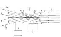
そこで、本発明では、レーザ発振器(図示省略)より照射されたレーザビーム5を、例えばプリズム3によりベッセルビーム4に形成して基板1の側面から照射する際に、図3に示すように、例えば基板1の上下位置にCCDカメラ6a、6bを設置するのと共に、例えば基板1の下方位置に傾きセンサー7を設置し、基板1の傾きを検出するのである。 Therefore, in the present invention, when the
このCCDカメラ6a、6bは、図4に示すように、前記照射したベッセルビーム4の基板1の上下面側の位置を映し出すことができるので、ベッセルビーム4の基板1の上下面側の位置を検出することができる。 As shown in FIG. 4, the
レーザ加工時は、プリズム3の位置、CCDカメラ6a、6bの相対位置関係は変化しない。従って、前記検出したベッセルビーム4の基板1の上下面側の位置により、レーザビーム5とプリズム3との位置決め(プリズム3の中心とレーザビーム5の中心を一致させる)を行い、さらに、基板1の上下面側の位置と、基板1の傾きに基づき、位置制御装置8で例えば基板1を動かし、ベッセルビーム4の基板1の上下面側の位置を移動させて加工位置の補正を行いつつ、基板1の端面部1aの加工を行うのである。 During laser processing, the position of the prism 3 and the relative positional relationship between the
このように、本発明では、ベッセルビーム4を基板1の側面から照射するので、加工面に対して線状の加工が可能となって、通常のピンポイントによる照射に比べて、加工効率が高くなり、基板1へのビームの照射時間を抑えて、熱的な負担が低減できる。 As described above, in the present invention, since the Bessel
そして、その際、ベッセルビーム4の基板1の上面側・下面側の位置と、基板1の位置関係を随時検出して加工位置を補正するので、ベッセルビーム4を基板1の側面から照射する際に、加工位置の裕度が小さいことにより、加工されない部分や加工むらの発生を防止することができる。 At that time, the position of the
また、本発明では、図5に示すように、レーザ加工時に集塵装置9を基板1の表面近傍まで近づけて配置することができるので、パーティクル10の除去を効率よく行うことができるという利点もある。 Further, in the present invention, as shown in FIG. 5, the dust collector 9 can be arranged close to the surface of the
上記本発明では、ベッセルビーム4の特性上、ビームが透過しない基板1には適用することができない。よって、ガラス樹脂や樹脂基板(シート・フィルム)など透明なものに限定されることは言うまでもない。 The above-described present invention cannot be applied to the
具体的には、本発明の適用対象としては、例えば太陽電池や液晶パネルを把持もしくは封止するために、基板の端部の導電性部材を除去するものが考えられる。 Specifically, as an object to which the present invention is applied, for example, in order to grip or seal a solar cell or a liquid crystal panel, one that removes the conductive member at the end of the substrate can be considered.
また、ベッセルビーム4の基板1の上下面側の位置をCCDカメラ6a、6bで検出する場合、CCDカメラ6a、6bに到達するビーム出力が大きい場合は、CCDカメラ6a、6bが損傷しないような手段を講じる必要がある。 Further, when the positions of the Bessel
例えば、ビーム出力を減衰するフィルター(減衰フィルター)をCCDカメラ6a、6bの直前に設けたり、また、CCDカメラ6a、6bの直前に感光フィルム(ビーム照射位置のみ色が変わる)を設置し、この感光フィルムを撮像する等すれば良い。 For example, a filter (attenuation filter) for attenuating the beam output is provided immediately before the
本発明は、上記の例に限るものではなく、各請求項に記載の技術的思想の範疇において、適宜実施の形態を変更しても良いことは言うまでもない。 The present invention is not limited to the above examples, and it goes without saying that the embodiments may be appropriately changed within the scope of the technical idea described in each claim.
例えば上記の例では、ベッセルビーム4の基板1の上下面側の位置を、2台のCCDカメラ6a、6bで検出しているが、1台のCCDカメラで基板1の加工側のみを検出するものでも良い。 For example, in the above example, the positions of the
また、ベッセルビーム4の位置の検出は、CCDカメラ以外でも可能である。ベッセルビーム4の位置検出部におけるビームの大きさは、加工条件にもよるが5mm程度であるので、光センサーや熱センサーを単数又は複数設置し、所定位置にベッセルビーム4が存在するか否かを検出することでベッセルビーム4の位置の検出を行うものでも良い。 Further, the position of the
また、上記の例では基板1を動かし、ベッセルビーム4を移動させて加工位置の補正を行うものを示したが、プリズム3を移動させても良い。また、ベッセルビーム4を形成できる光学部材であれば、プリズム3に限らず、円錐レンズ(アキシコンレンズ)等、公知のものが使用できる。 In the above example, the
本発明は、導電性部材の除去だけでなく、被加工物の端面部にビームを照射する必要のある加工であれば、微細加工等、どのようなレーザ加工にも適用が可能である。 The present invention can be applied not only to the removal of the conductive member but also to any laser processing such as micromachining as long as it is necessary to irradiate the end face of the workpiece with a beam.
1 基板
1a 端面部
3 プリズム
4 ベッセルビーム
5 レーザビーム
6a、6b CCDカメラ
7 傾き検出センサー
8 位置制御装置DESCRIPTION OF
Claims (2)
Translated fromJapaneseベッセルビームの照射を前記基板の側面から行い、かつ、照射したベッセルビームと基板の加工位置との相対位置関係を検出しながら加工位置の補正を行いつつ、前記端面部の加工を行うことを特徴とするレーザ加工方法。A method of laser processing an end surface portion of a substrate by irradiating a substrate with a Bessel beam,
Irradiating the Bessel beam from the side surface of the substrate, and processing the end face while correcting the processing position while detecting the relative positional relationship between the irradiated Bessel beam and the processing position of the substrate. A laser processing method.
レーザビームを照射するレーザ発振器と、
このレーザ発振器より照射されたレーザビームをベッセルビームに形成する光学部材と、
基板側面から照射した、前記光学部材により形成されたベッセルビームと、基板の加工位置を検出する検出器と、
基板の傾きを検出する検出器と、
これら検出器により検出したベッセルビームと、基板の加工位置及び基板の傾きに基づき、基板、光学部材の少なくとも何れか一つの位置を制御してベッセルビームによる加工位置の補正を行う位置制御装置を備えたことを特徴とするレーザ加工装置。An apparatus that irradiates a substrate with a Bessel beam and laser-processes an end surface portion of the substrate,
A laser oscillator for irradiating a laser beam;
An optical member for forming a laser beam irradiated from the laser oscillator into a Bessel beam;
A Bessel beam formed by the optical member irradiated from the side surface of the substrate, a detector for detecting a processing position of the substrate,
A detector for detecting the tilt of the substrate;
Based on the Bessel beam detected by these detectors, the processing position of the substrate, and the tilt of the substrate, a position control device is provided that corrects the processing position by the Bessel beam by controlling the position of at least one of the substrate and the optical member. A laser processing apparatus characterized by that.
Priority Applications (1)
| Application Number | Priority Date | Filing Date | Title |
|---|---|---|---|
| JP2010009073AJP5461205B2 (en) | 2010-01-19 | 2010-01-19 | Laser processing method and apparatus |
Applications Claiming Priority (1)
| Application Number | Priority Date | Filing Date | Title |
|---|---|---|---|
| JP2010009073AJP5461205B2 (en) | 2010-01-19 | 2010-01-19 | Laser processing method and apparatus |
Publications (2)
| Publication Number | Publication Date |
|---|---|
| JP2011147943A JP2011147943A (en) | 2011-08-04 |
| JP5461205B2true JP5461205B2 (en) | 2014-04-02 |
Family
ID=44535443
Family Applications (1)
| Application Number | Title | Priority Date | Filing Date |
|---|---|---|---|
| JP2010009073AExpired - Fee RelatedJP5461205B2 (en) | 2010-01-19 | 2010-01-19 | Laser processing method and apparatus |
Country Status (1)
| Country | Link |
|---|---|
| JP (1) | JP5461205B2 (en) |
Families Citing this family (15)
| Publication number | Priority date | Publication date | Assignee | Title |
|---|---|---|---|---|
| EP2754524B1 (en) | 2013-01-15 | 2015-11-25 | Corning Laser Technologies GmbH | Method of and apparatus for laser based processing of flat substrates being wafer or glass element using a laser beam line |
| EP2781296B1 (en) | 2013-03-21 | 2020-10-21 | Corning Laser Technologies GmbH | Device and method for cutting out contours from flat substrates using a laser |
| US10293436B2 (en) | 2013-12-17 | 2019-05-21 | Corning Incorporated | Method for rapid laser drilling of holes in glass and products made therefrom |
| US11556039B2 (en) | 2013-12-17 | 2023-01-17 | Corning Incorporated | Electrochromic coated glass articles and methods for laser processing the same |
| CN106687419A (en) | 2014-07-08 | 2017-05-17 | 康宁股份有限公司 | Methods and apparatuses for laser processing materials |
| KR20170028943A (en) | 2014-07-14 | 2017-03-14 | 코닝 인코포레이티드 | System for and method of processing transparent materials using laser beam focal lines adjustable in length and diameter |
| US10047001B2 (en)* | 2014-12-04 | 2018-08-14 | Corning Incorporated | Glass cutting systems and methods using non-diffracting laser beams |
| HUE055461T2 (en) | 2015-03-24 | 2021-11-29 | Corning Inc | Laser cutting and processing of display glass compositions |
| DE102015110422A1 (en) | 2015-06-29 | 2016-12-29 | Schott Ag | Laser processing of a multiphase transparent material, as well as multiphase composite material |
| JP7082042B2 (en) | 2015-07-10 | 2022-06-07 | コーニング インコーポレイテッド | A method for continuously forming holes in a flexible substrate sheet and related products. |
| US10730783B2 (en) | 2016-09-30 | 2020-08-04 | Corning Incorporated | Apparatuses and methods for laser processing transparent workpieces using non-axisymmetric beam spots |
| EP3529214B1 (en) | 2016-10-24 | 2020-12-23 | Corning Incorporated | Substrate processing station for laser-based machining of sheet-like glass substrates |
| CN110174770B (en)* | 2019-03-18 | 2023-10-27 | 首都师范大学 | A device and method for generating Bessel beams with multi-segment stable transmission on an axis |
| CN110237875B (en)* | 2019-05-31 | 2020-11-10 | 西安交通大学 | Mark-free living cell detection micro-fluidic chip based on quasi-Bessel optical waveguide structure |
| CN111203651B (en)* | 2020-01-15 | 2021-06-22 | 北京理工大学 | Method for processing and calculating hologram in transparent material by space shaping femtosecond laser |
Family Cites Families (4)
| Publication number | Priority date | Publication date | Assignee | Title |
|---|---|---|---|---|
| JP2541440B2 (en)* | 1993-03-17 | 1996-10-09 | 日本電気株式会社 | Laser process equipment |
| JP2004042140A (en)* | 2002-07-12 | 2004-02-12 | Hitachi Zosen Corp | Thin film removing method and apparatus |
| JP4418282B2 (en)* | 2004-03-31 | 2010-02-17 | 株式会社レーザーシステム | Laser processing method |
| DE102007024700A1 (en)* | 2007-05-25 | 2008-12-04 | Fraunhofer-Gesellschaft zur Förderung der angewandten Forschung e.V. | Method for processing materials with laser radiation and apparatus for carrying out the method |
- 2010
- 2010-01-19JPJP2010009073Apatent/JP5461205B2/ennot_activeExpired - Fee Related
Also Published As
| Publication number | Publication date |
|---|---|
| JP2011147943A (en) | 2011-08-04 |
Similar Documents
| Publication | Publication Date | Title |
|---|---|---|
| JP5461205B2 (en) | Laser processing method and apparatus | |
| CN108568593B (en) | Laser processing device | |
| JP4668809B2 (en) | Surface inspection device | |
| CN101647126B (en) | Method for laser ablation of solar cells | |
| JP7475782B2 (en) | Processing Equipment | |
| KR102231739B1 (en) | Method of inspecting laser beam | |
| CN205702840U (en) | Laser machine for double-sided processing | |
| JP5242036B2 (en) | Laser processing equipment | |
| TWI864297B (en) | Processing equipment | |
| TW202238796A (en) | Processing device | |
| KR20210031605A (en) | Position adjusting method and apparatus thereof | |
| KR102333514B1 (en) | Method for testing laser beam | |
| JP5301919B2 (en) | Hard brittle plate chamfering device | |
| JP4801634B2 (en) | Laser processing apparatus and laser processing method | |
| JP2006315086A (en) | Apparatus and method for laser beam machining | |
| CN112338352B (en) | Method for confirming processing performance of laser processing equipment | |
| JP2006315085A (en) | Apparatus for laser beam machining | |
| JP6313148B2 (en) | Marking device | |
| JP2022186378A (en) | LASER PROCESSING METHOD AND LASER PROCESSING APPARATUS | |
| JP7617772B2 (en) | Laser processing equipment | |
| JP2021141135A (en) | Laser processing method and reformer | |
| JP7704638B2 (en) | processing equipment | |
| KR102594218B1 (en) | Machining apparatus | |
| JP4906378B2 (en) | Method for detecting posture of laser processing mask and method for evaluating stage accuracy | |
| JP4493428B2 (en) | Foreign matter inspection apparatus and foreign matter inspection method |
Legal Events
| Date | Code | Title | Description |
|---|---|---|---|
| A621 | Written request for application examination | Free format text:JAPANESE INTERMEDIATE CODE: A621 Effective date:20121220 | |
| TRDD | Decision of grant or rejection written | ||
| A977 | Report on retrieval | Free format text:JAPANESE INTERMEDIATE CODE: A971007 Effective date:20131212 | |
| A01 | Written decision to grant a patent or to grant a registration (utility model) | Free format text:JAPANESE INTERMEDIATE CODE: A01 Effective date:20131217 | |
| A61 | First payment of annual fees (during grant procedure) | Free format text:JAPANESE INTERMEDIATE CODE: A61 Effective date:20140115 | |
| R150 | Certificate of patent or registration of utility model | Ref document number:5461205 Country of ref document:JP Free format text:JAPANESE INTERMEDIATE CODE: R150 Free format text:JAPANESE INTERMEDIATE CODE: R150 | |
| LAPS | Cancellation because of no payment of annual fees |