JP5459910B2 - Display device - Google Patents
Display deviceDownload PDFInfo
- Publication number
- JP5459910B2 JP5459910B2JP2010151515AJP2010151515AJP5459910B2JP 5459910 B2JP5459910 B2JP 5459910B2JP 2010151515 AJP2010151515 AJP 2010151515AJP 2010151515 AJP2010151515 AJP 2010151515AJP 5459910 B2JP5459910 B2JP 5459910B2
- Authority
- JP
- Japan
- Prior art keywords
- light
- transistor
- substrate
- touch panel
- signal line
- Prior art date
- Legal status (The legal status is an assumption and is not a legal conclusion. Google has not performed a legal analysis and makes no representation as to the accuracy of the status listed.)
- Expired - Fee Related
Links
Images


Classifications
- G—PHYSICS
- G06—COMPUTING OR CALCULATING; COUNTING
- G06F—ELECTRIC DIGITAL DATA PROCESSING
- G06F3/00—Input arrangements for transferring data to be processed into a form capable of being handled by the computer; Output arrangements for transferring data from processing unit to output unit, e.g. interface arrangements
- G06F3/01—Input arrangements or combined input and output arrangements for interaction between user and computer
- G06F3/03—Arrangements for converting the position or the displacement of a member into a coded form
- G06F3/041—Digitisers, e.g. for touch screens or touch pads, characterised by the transducing means
- G06F3/042—Digitisers, e.g. for touch screens or touch pads, characterised by the transducing means by opto-electronic means
- G—PHYSICS
- G02—OPTICS
- G02F—OPTICAL DEVICES OR ARRANGEMENTS FOR THE CONTROL OF LIGHT BY MODIFICATION OF THE OPTICAL PROPERTIES OF THE MEDIA OF THE ELEMENTS INVOLVED THEREIN; NON-LINEAR OPTICS; FREQUENCY-CHANGING OF LIGHT; OPTICAL LOGIC ELEMENTS; OPTICAL ANALOGUE/DIGITAL CONVERTERS
- G02F1/00—Devices or arrangements for the control of the intensity, colour, phase, polarisation or direction of light arriving from an independent light source, e.g. switching, gating or modulating; Non-linear optics
- G02F1/01—Devices or arrangements for the control of the intensity, colour, phase, polarisation or direction of light arriving from an independent light source, e.g. switching, gating or modulating; Non-linear optics for the control of the intensity, phase, polarisation or colour
- G02F1/13—Devices or arrangements for the control of the intensity, colour, phase, polarisation or direction of light arriving from an independent light source, e.g. switching, gating or modulating; Non-linear optics for the control of the intensity, phase, polarisation or colour based on liquid crystals, e.g. single liquid crystal display cells
- G02F1/133—Constructional arrangements; Operation of liquid crystal cells; Circuit arrangements
- G02F1/1333—Constructional arrangements; Manufacturing methods
- G02F1/13338—Input devices, e.g. touch panels
- G—PHYSICS
- G06—COMPUTING OR CALCULATING; COUNTING
- G06F—ELECTRIC DIGITAL DATA PROCESSING
- G06F3/00—Input arrangements for transferring data to be processed into a form capable of being handled by the computer; Output arrangements for transferring data from processing unit to output unit, e.g. interface arrangements
- G06F3/01—Input arrangements or combined input and output arrangements for interaction between user and computer
- G06F3/03—Arrangements for converting the position or the displacement of a member into a coded form
- G06F3/0304—Detection arrangements using opto-electronic means
- G—PHYSICS
- G06—COMPUTING OR CALCULATING; COUNTING
- G06F—ELECTRIC DIGITAL DATA PROCESSING
- G06F3/00—Input arrangements for transferring data to be processed into a form capable of being handled by the computer; Output arrangements for transferring data from processing unit to output unit, e.g. interface arrangements
- G06F3/01—Input arrangements or combined input and output arrangements for interaction between user and computer
- G06F3/03—Arrangements for converting the position or the displacement of a member into a coded form
- G06F3/041—Digitisers, e.g. for touch screens or touch pads, characterised by the transducing means
- G06F3/0412—Digitisers structurally integrated in a display
- G—PHYSICS
- G06—COMPUTING OR CALCULATING; COUNTING
- G06F—ELECTRIC DIGITAL DATA PROCESSING
- G06F3/00—Input arrangements for transferring data to be processed into a form capable of being handled by the computer; Output arrangements for transferring data from processing unit to output unit, e.g. interface arrangements
- G06F3/01—Input arrangements or combined input and output arrangements for interaction between user and computer
- G06F3/03—Arrangements for converting the position or the displacement of a member into a coded form
- G06F3/041—Digitisers, e.g. for touch screens or touch pads, characterised by the transducing means
- G06F3/0416—Control or interface arrangements specially adapted for digitisers
- G06F3/04166—Details of scanning methods, e.g. sampling time, grouping of sub areas or time sharing with display driving
- H—ELECTRICITY
- H10—SEMICONDUCTOR DEVICES; ELECTRIC SOLID-STATE DEVICES NOT OTHERWISE PROVIDED FOR
- H10K—ORGANIC ELECTRIC SOLID-STATE DEVICES
- H10K59/00—Integrated devices, or assemblies of multiple devices, comprising at least one organic light-emitting element covered by group H10K50/00
- H10K59/40—OLEDs integrated with touch screens
- G—PHYSICS
- G06—COMPUTING OR CALCULATING; COUNTING
- G06F—ELECTRIC DIGITAL DATA PROCESSING
- G06F2203/00—Indexing scheme relating to G06F3/00 - G06F3/048
- G06F2203/041—Indexing scheme relating to G06F3/041 - G06F3/045
- G06F2203/04107—Shielding in digitiser, i.e. guard or shielding arrangements, mostly for capacitive touchscreens, e.g. driven shields, driven grounds
Landscapes
- Engineering & Computer Science (AREA)
- General Engineering & Computer Science (AREA)
- Theoretical Computer Science (AREA)
- Physics & Mathematics (AREA)
- General Physics & Mathematics (AREA)
- Human Computer Interaction (AREA)
- Nonlinear Science (AREA)
- Liquid Crystal (AREA)
- Chemical & Material Sciences (AREA)
- Crystallography & Structural Chemistry (AREA)
- Mathematical Physics (AREA)
- Optics & Photonics (AREA)
- Position Input By Displaying (AREA)
- Devices For Indicating Variable Information By Combining Individual Elements (AREA)
Description
Translated fromJapanese本発明は、タッチセンサを有するタッチパネルと、その駆動方法に関する。特に、タッチセンサを有する画素がマトリックス状に配置されたタッチパネルと、その駆動方法に関する。更には、当該タッチパネルを有する電子機器に関する。The present invention relates to a touch panel having a touch sensor and a driving method thereof. In particular, the present invention relates to a touch panel in which pixels having touch sensors are arranged in a matrix and a driving method thereof. Furthermore, the present invention relates to an electronic device having the touch panel.
近年、タッチセンサを搭載した表示装置が注目されている。タッチセンサを搭載した表示装置は、タッチパネル又はタッチスクリーンなどと呼ばれている(以下、これを単に「タッチパネル」と呼ぶ)。タッチセンサには、動作原理の違いにより、抵抗膜方式、静電容量方式、光方式などがある。いずれの方式においても、被検出物が表示装置に接触もしくは近接することでデータを入力することができる。In recent years, display devices equipped with touch sensors have attracted attention. A display device equipped with a touch sensor is called a touch panel or a touch screen (hereinafter simply referred to as “touch panel”). The touch sensor includes a resistance film method, a capacitance method, an optical method, and the like depending on a difference in operation principle. In either method, data can be input when the object to be detected is in contact with or close to the display device.
光方式のタッチセンサとして光を検出するセンサ(「フォトセンサ」ともいう)をタッチパネルに設けることにより、表示画面が入力領域を兼ねる。このような光方式のタッチセンサを有する装置の一例として、画像取り込みを行う密着型エリアセンサを配置することによって画像取り込み機能を備えた表示装置が挙げられる(例えば、特許文献1を参照)。光方式のタッチセンサを有するタッチパネルでは、タッチパネルから光が発せられる。タッチパネルの任意の位置に被検出物が存在する場合には、被検出物が存在する領域の光が被検出物によって遮断され、一部の光が反射される。タッチパネル内の画素には光を検出することができるフォトセンサ(「光電変換素子」と呼ばれることもある。)が設けられており、反射された光を検出することで、光が検出された領域に被検出物が存在することを認識することができる。By providing a sensor for detecting light (also referred to as a “photo sensor”) as an optical touch sensor on the touch panel, the display screen also serves as an input area. As an example of a device having such an optical touch sensor, a display device having an image capturing function by disposing a contact area sensor that captures an image can be given (for example, see Patent Document 1). In a touch panel having an optical touch sensor, light is emitted from the touch panel. When an object to be detected exists at an arbitrary position on the touch panel, light in a region where the object to be detected exists is blocked by the object to be detected, and a part of the light is reflected. A pixel in the touch panel is provided with a photosensor (sometimes referred to as a “photoelectric conversion element”) that can detect light, and an area in which light is detected by detecting reflected light. It can be recognized that an object to be detected exists.
また、携帯電話、携帯情報端末をはじめとする電子機器に、本人認証機能等を付与する試みがなされている(例えば、特許文献2を参照)。本人認証には、指紋、顔、手形、掌紋及び手の静脈の形状等が用いられる。本人認証機能を表示部とは別の部分に設ける場合には、部品点数が増大し、電子機器の重量や価格が増大するおそれがある。In addition, attempts have been made to provide a personal authentication function or the like to electronic devices such as mobile phones and portable information terminals (see, for example, Patent Document 2). For personal authentication, fingerprints, faces, handprints, palm prints, hand vein shapes, and the like are used. When the personal authentication function is provided in a part other than the display unit, the number of parts increases, which may increase the weight and price of the electronic device.
また、タッチセンサのシステムにおいて、外光の明るさに応じて指先の位置を検出するための画像処理方法を選択する技術が知られている(例えば、特許文献3を参照)。In addition, in a touch sensor system, a technique for selecting an image processing method for detecting the position of a fingertip according to the brightness of external light is known (see, for example, Patent Document 3).
本人認証機能を有する電子機器にタッチパネルを用いる際には、タッチパネルの各画素に設けられたフォトセンサが光を検出して生成した電気信号を収集し、画像処理を施す必要がある。特に、高分解能、高速動作の本人認証機能を有する電子機器を実現するには、フォトセンサの高感度化が要求される。さらに、高度な本人認証機能を実現するためには、モノクロではなく、カラーでのデータ収集が必要になる。また、安価にタッチパネルを提供する必要がある。When a touch panel is used for an electronic device having a personal authentication function, it is necessary to collect an electric signal generated by detecting light by a photosensor provided in each pixel of the touch panel and perform image processing. In particular, in order to realize an electronic device having a high-resolution and high-speed personal authentication function, it is necessary to increase the sensitivity of the photosensor. Furthermore, in order to realize an advanced authentication function, it is necessary to collect data in color instead of monochrome. In addition, it is necessary to provide a touch panel at a low cost.
上記の課題に鑑み、開示する発明の一態様は、高感度のフォトセンサを有し、カラーでの撮像機能を有する安価なタッチパネル及びその駆動方法を提供することを目的の一つとする。In view of the above problems, an object of one embodiment of the disclosed invention is to provide an inexpensive touch panel that includes a high-sensitivity photosensor and has a color imaging function and a driving method thereof.
本発明の一態様におけるタッチパネルは、画素に表示素子とフォトセンサとを各々有し、フォトセンサが有するフォトダイオードと、表示素子が有する薄膜トランジスタとは、共通の半導体膜から構成され、バックライトを対向基板側から照射し、TFT基板側に被検出物を配置して使用し、バックライトは複数の特定の色の光源を順次点灯することで構成し、当該色の光源が点灯している期間にフォトセンサより被検出物からの反射光を検出して当該色の撮像データとし、全ての色の撮像データからカラーの撮像画像を構成する。また、本発明の一態様におけるタッチパネルは、薄膜トランジスタのゲート電極を構成する導電膜で、フォトダイオードの遮蔽膜を構成する。The touch panel according to one embodiment of the present invention includes a pixel including a display element and a photosensor, and the photodiode included in the photosensor and the thin film transistor included in the display element are each formed using a common semiconductor film and face the backlight. Irradiate from the substrate side, place the object to be detected on the TFT substrate side, and use the backlight by turning on a plurality of specific color light sources in sequence. The reflected light from the object to be detected is detected by the photo sensor to obtain the image data of that color, and a color image is formed from the image data of all colors. The touch panel of one embodiment of the present invention includes a conductive film that forms a gate electrode of a thin film transistor and a shielding film of a photodiode.
本発明により、高分解能でカラーでの撮像が可能な安価なタッチパネルを提供することができる。また、高分解能でカラーでの撮像が可能な安価なタッチパネルの駆動方法を提供することができる。According to the present invention, it is possible to provide an inexpensive touch panel that can perform color imaging with high resolution. In addition, it is possible to provide an inexpensive touch panel driving method capable of color imaging with high resolution.
以下に、実施の形態について、図面を用いて詳細に説明する。但し、以下の実施の形態は多くの異なる態様で実施することが可能であり、趣旨及びその範囲から逸脱することなくその形態及び詳細を様々に変更し得ることは、当業者であれば容易に理解される。従って、以下に示す実施の形態の記載内容に限定して解釈されるものではない。なお、実施の形態を説明するための全図において、同一部分又は同様な機能を有する部分には同一の符号を付し、その繰り返しの説明は省略する。Hereinafter, embodiments will be described in detail with reference to the drawings. However, the following embodiments can be implemented in many different modes, and it is easy for those skilled in the art to change the modes and details in various ways without departing from the spirit and scope thereof. Understood. Therefore, the present invention is not construed as being limited to the description of the embodiments below. Note that in all the drawings for describing the embodiments, the same portions or portions having similar functions are denoted by the same reference numerals, and repetitive description thereof is omitted.
(実施の形態1)
本実施の形態では、タッチパネルについて図1〜図5を参照して説明する。(Embodiment 1)
In this embodiment, a touch panel will be described with reference to FIGS.
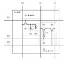
タッチパネルの構成について、図1を参照して説明する。タッチパネル100は、画素回路101、表示素子制御回路102及びフォトセンサ制御回路103を有する。画素回路101は、行列方向にマトリクス状に配置された複数の画素104を有する。各々の画素104は、表示素子105とフォトセンサ106を有する。The configuration of the touch panel will be described with reference to FIG. The touch panel 100 includes a
表示素子105は、薄膜トランジスタ(Thin Film Transistor:TFT)、保持容量、液晶層を有する液晶素子などを有する。薄膜トランジスタは、保持容量への電荷を注入もしくは排出を制御する機能を有する。保持容量は、液晶層に印加する電圧に相当する電荷を保持する機能を有する。液晶層に電圧を印加することで偏光方向が変化することを利用して、液晶層を透過する光の明暗(階調)を作ることで、画像表示が実現される。液晶層を透過する光には、光源(バックライト)によって液晶表示装置の裏面から照射される光を用いる。The
なお、カラー画像表示を行う方式として、カラーフィルタを用いる方式、所謂、カラーフィルタ方式がある。これは、液晶層を透過した光がカラーフィルタを通過することで、特定の色(例えば、赤(R)、緑(G)、青(B))の階調を作ることができる。ここで、カラーフィルタ方式を用いる際に、赤(R)、緑(G)、青(B)のいずれかの色を発光する機能を有する画素104を、各々、R画素、G画素、B画素と呼ぶことにする。As a method for displaying a color image, there is a so-called color filter method using a color filter. This is because the light transmitted through the liquid crystal layer passes through the color filter, so that gradations of specific colors (for example, red (R), green (G), and blue (B)) can be created. Here, when the color filter method is used, the
また、カラー画像表示を行う別の方式として、バックライトを特定の色(例えば、赤(R)、緑(G)、青(B))の光源で構成して各色を順次点灯する方式、所謂、フィールドシーケンシャル方式がある。フィールドシーケンシャル方式では、各色の光源が点灯している期間に、液晶層を透過する光の明暗を作ることで、当該色の階調を作ることができる。As another method for displaying a color image, a backlight is composed of light sources of specific colors (for example, red (R), green (G), and blue (B)), and each color is sequentially turned on, so-called. There is a field sequential method. In the field sequential method, the gradation of the color can be made by making the light transmitted through the liquid crystal layer light and dark while the light source of each color is on.
なお、表示素子105が液晶素子を有する場合について説明したが、発光素子などの他の素子を有していてもよい。発光素子は、電流または電圧によって輝度が制御される素子であり、具体的には発光ダイオード、OLED(Organic Light Emitting Diode)等が挙げられる。Note that although the case where the
フォトセンサ106は、フォトダイオードなど、受光することで電気信号を発する機能を有する素子と、薄膜トランジスタとを有する。なお、フォトセンサ106が受光する光は、バックライトからの光が、被検出物に照射された際の反射光を利用する。The
表示素子制御回路102は、表示素子105を制御するための回路であり、ビデオデータ信号線などの信号線(「ソース信号線」ともいう。)を介して表示素子105に信号を入力する表示素子駆動回路107と、走査線(「ゲート信号線」ともいう。)を介して表示素子105に信号を入力する表示素子駆動回路108を有する。例えば、走査線側の表示素子駆動回路108は、特定の行に配置された画素が有する表示素子を選択する機能を有する。また、信号線側の表示素子駆動回路107は、選択された行の画素が有する表示素子に任意の電位を与える機能を有する。なお、走査線側の表示素子駆動回路108により高電位を印加された表示素子では、薄膜トランジスタが導通状態となり、信号線側の表示素子駆動回路107により与えられる電荷が供給される。The display element control circuit 102 is a circuit for controlling the
フォトセンサ制御回路103は、フォトセンサ106を制御するための回路であり、フォトセンサ出力信号線、フォトセンサ基準信号線等の信号線側のフォトセンサ読み出し回路109と、走査線側のフォトセンサ駆動回路110を有する。例えば、走査線側のフォトセンサ駆動回路110は、特定の行に配置された画素が有するフォトセンサ106を選択する機能を有する。また、信号線側のフォトセンサ読み出し回路109は、選択された行の画素が有するフォトセンサ106の出力信号を取り出す機能を有する。なお、信号線側のフォトセンサ読み出し回路109は、アナログ信号であるフォトセンサの出力を、OPアンプを用いてアナログ信号のままタッチパネル外部に取り出す構成や、A/D変換回路を用いてデジタル信号に変換してからタッチパネル外部に取り出す構成が考え得る。The photosensor control circuit 103 is a circuit for controlling the
画素104の回路図について、図2を用いて説明する。画素104は、トランジスタ201、保持容量202及び液晶素子203を有する表示素子105と、フォトダイオード204、トランジスタ205及びトランジスタ206を有するフォトセンサ106とを有する。A circuit diagram of the
トランジスタ201は、ゲートがゲート信号線207に、ソース又はドレインの一方がビデオデータ信号線210に、ソース又はドレインの他方が保持容量202の一方の電極と液晶素子203の一方の電極に電気的に接続されている。保持容量202の他方の電極と液晶素子203の他方の電極は一定の電位に保たれている。液晶素子203は、一対の電極と、該一対の電極の間に液晶層を含む素子である。In the
トランジスタ201は、ゲート信号線207に電位”H”(ハイレベルの電位)が印加されると、ビデオデータ信号線210の電位を保持容量202と液晶素子203に印加する。保持容量202は、印加された電位を保持する。液晶素子203は、印加された電位により、光の透過率を変更する。When the potential “H” (high level potential) is applied to the
フォトダイオード204は、一方の電極がフォトダイオードリセット信号線208に、他方の電極がトランジスタ205のゲートに電気的に接続されている。トランジスタ205は、ソース又はドレインの一方がフォトセンサ出力信号線211に、ソース又はドレインの他方がトランジスタ206のソース又はドレインの一方に電気的に接続されている。トランジスタ206は、ゲートがゲート信号線209に、ソース又はドレインの他方がフォトセンサ基準信号線212に電気的に接続されている。The
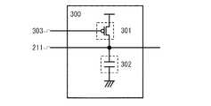
次に、フォトセンサ読み出し回路109の構成について、図3を用いて説明する。図3において、画素1列分に対応するフォトセンサ読み出し回路300は、p型TFT301、保持容量302、を有する。また、当該画素列のフォトセンサ出力信号線211、プリチャージ信号線303を有する。Next, the configuration of the photosensor readout circuit 109 will be described with reference to FIG. In FIG. 3, the
フォトセンサ読み出し回路300では、画素内におけるフォトセンサの動作に先立ち、フォトセンサ出力信号線211の電位を基準電位に設定する。図3では、プリチャージ信号線303の電位を”L”(ローレベルの電位)とすることで、フォトセンサ出力信号線211を基準電位である高電位に設定することができる。なお、保持容量302は、フォトセンサ出力信号線211の寄生容量が大きい場合には、特別に設けなくても良い。なお、基準電位を、低電位とする構成も可能である。この場合、n型TFTを用いることで、プリチャージ信号線303の電位を”H”とすることで、フォトセンサ出力信号線211を基準電位である低電位に設定することができる。In the photo
次に、本タッチパネルにおけるフォトセンサの読み出し動作について、図4のタイミングチャートを用いて説明する。図4において、信号401〜信号404は、図2におけるフォトダイオードリセット信号線208、トランジスタ206のゲートが接続されたゲート信号線209、トランジスタ205のゲートが接続されたゲート信号線213、フォトセンサ出力信号線211の電位にそれぞれ相当する。また、信号405は、図3におけるプリチャージ信号線303の電位に相当する。Next, the reading operation of the photosensor in this touch panel will be described with reference to the timing chart of FIG. 4, the
時刻Aにおいて、フォトダイオードリセット信号線208の電位(信号401)を”H”とすると、フォトダイオード204が導通し、トランジスタ205のゲートが接続されたゲート信号線213の電位(信号403)が”H”となる。また、プリチャージ信号線303の電位(信号405)は”L”とすると、フォトセンサ出力信号線211の電位(信号404)は”H”にプリチャージされる。At time A, when the potential of the photodiode reset signal line 208 (signal 401) is set to “H”, the
時刻Bにおいて、フォトダイオードリセット信号線208の電位(信号401)を”L”にすると、フォトダイオード204のオフ電流により、トランジスタ205のゲートが接続されたゲート信号線213の電位(信号403)が低下し始める。フォトダイオード204は、光が照射されるとオフ電流が増大するので、照射される光の量に応じてトランジスタ205のゲートが接続されたゲート信号線213の電位(信号403)は変化する。すなわち、トランジスタ205のソースとドレイン間の電流が変化する。At time B, when the potential of the photodiode reset signal line 208 (signal 401) is set to “L”, the potential of the
時刻Cにおいて、ゲート信号線209の電位(信号402)を”H”にすると、トランジスタ206が導通し、フォトセンサ基準信号線212とフォトセンサ出力信号線211とが、トランジスタ205とトランジスタ206とを介して導通する。すると、フォトセンサ出力信号線211の電位(信号404)は、低下していく。なお、時刻C以前に、プリチャージ信号線303の電位(信号405)は”H”とし、フォトセンサ出力信号線211のプリチャージを終了しておく。ここで、フォトセンサ出力信号線211の電位(信号404)が低下する速さは、トランジスタ205のソースとドレイン間の電流に依存する。すなわち、フォトダイオード204に照射されている光の量に応じて変化する。At time C, when the potential of the gate signal line 209 (signal 402) is set to “H”, the
時刻Dにおいて、ゲート信号線209の電位(信号402)を”L”にすると、トランジスタ206が遮断され、フォトセンサ出力信号線211の電位(信号404)は、時刻D以後、一定値となる。ここで、一定値となる値は、フォトダイオード204に照射されている光の量に応じて変化する。したがって、フォトセンサ出力信号線211の電位を取得することで、フォトダイオード204に照射されている光の量を知ることができる。When the potential of the gate signal line 209 (signal 402) is set to “L” at time D, the
図5に、タッチパネルの断面図の一例を示す。図5に示すタッチパネルでは、絶縁表面を有する基板(TFT基板)1001上に、フォトダイオード1002、トランジスタ1003、保持容量1004、液晶素子1005が設けられている。FIG. 5 shows an example of a cross-sectional view of the touch panel. In the touch panel illustrated in FIG. 5, a
フォトダイオード1002と、保持容量1004とは、トランジスタ1003を作製するプロセスにおいて、トランジスタ1003と共に形成することが可能である。フォトダイオード1002は横型接合タイプのpinダイオードであり、フォトダイオード1002が有する半導体膜1006は、p型の導電性を有する領域(p層)と、i型の導電性を有する領域(i層)と、n型の導電性を有する領域(n層)とを有している。なお、本実施の形態では、フォトダイオード1002がpinダイオードである場合を例示しているが、フォトダイオード1002はpnダイオードであっても良い。横型接合タイプのpinダイオードまたはpnダイオードは、p型を付与する不純物と、n型を付与する不純物とを、それぞれ半導体膜1006の特定の領域に添加することで、形成することが出来る。The
また、TFT基板1001上に成膜した一の半導体膜をエッチングなどにより所望の形状に加工(パターニング)することで、フォトダイオード1002の島状の半導体膜と、トランジスタ1003の島状の半導体膜とを一緒に形成することができ、通常のパネル作製プロセスに追加するプロセスが不要となり、コストを低減できる。Further, by processing (patterning) one semiconductor film formed over the
液晶素子1005は、画素電極1007と、液晶1008と、対向電極1009とを有する。画素電極1007は基板1001上に形成されており、トランジスタ1003及び保持容量1004と、導電膜1010を介して電気的に接続されている。また、対向電極1009は、基板(対向基板)1013上に形成されており、画素電極1007と対向電極1009の間に、液晶1008が挟まれている。なお、図5では、フォトセンサに用いられているトランジスタについては図示していないが、当該トランジスタも、トランジスタ1003を作製するプロセスにおいて、トランジスタ1003と共に基板(TFT基板)1001上に形成することが可能である。The
画素電極1007と、対向電極1009の間のセルギャップは、スペーサー1016を用いて制御することが出来る。図5では、フォトリソグラフィーで選択的に形成された柱状のスペーサー1016を用いてセルギャップを制御しているが、球状のスペーサーを画素電極1007と対向電極1009の間に分散させることで、セルギャップを制御することも出来る。A cell gap between the
また液晶1008は、基板(TFT基板)1001と基板(対向基板)1013の間において、封止材により囲まれている。液晶1008の注入は、ディスペンサ式(滴下式)を用いても良いし、ディップ式(汲み上げ式)を用いていても良い。The
画素電極1007には、透光性を有する導電性材料、例えばインジウム錫酸化物(ITO)、酸化亜鉛(ZnO)、酸化珪素を含むインジウム錫酸化物(ITSO)、有機インジウム、有機スズ、酸化亜鉛(ZnO)を含むインジウム亜鉛酸化物(IZO(Indium Zinc Oxide))、ガリウム(Ga)を含む酸化亜鉛、酸化スズ(SnO2)、酸化タングステンを含むインジウム酸化物、酸化タングステンを含むインジウム亜鉛酸化物、酸化チタンを含むインジウム酸化物、酸化チタンを含むインジウム錫酸化物などを用いることが出来る。The
また、本実施の形態では、透過型の液晶素子1005を例に挙げているので、画素電極1007と同様に、対向電極1009にも上述した透光性を有する導電性材料を用いることが出来る。In this embodiment, since the transmissive
画素電極1007と液晶1008の間には配向膜1011が、対向電極1009と液晶1008の間には配向膜1012が、それぞれ設けられている。配向膜1011、配向膜1012はポリイミド、ポリビニルアルコールなどの有機樹脂を用いて形成することができ、その表面には、ラビングなどの、液晶分子を一定方向に配列させるための配向処理が施されている。ラビングは、配向膜に圧力をかけながら、ナイロンなどの布を巻いたローラーを回転させて、上記配向膜の表面を一定方向に擦ることで、行うことが出来る。なお、酸化珪素などの無機材料を用い、配向処理を施すことなく、蒸着法で配向特性を有する配向膜1011、配向膜1012を直接形成することも可能である。An
また、液晶素子1005と重なるように、特定の波長領域の光を通すことができるカラーフィルタ1014が、基板(対向基板)1013上に形成されている。カラーフィルタ1014は、顔料を分散させたアクリル系樹脂などの有機樹脂を基板1013上に塗布した後、フォトリソグラフィーを用いて選択的に形成することができる。また、顔料を分散させたポリイミド系樹脂を基板1013上に塗布した後、エッチングを用いて選択的に形成することもできる。或いは、インクジェットなどの液滴吐出法を用いることで、選択的にカラーフィルタ1014を形成することもできる。In addition, a
また、フォトダイオード1002と重なるように、光を遮蔽することが出来る遮蔽膜1015が、基板(対向基板)1013上に形成されている。遮蔽膜1015を設けることで、基板(対向基板)1013を透過してタッチパネル内に入射したバックライトからの光が、直接フォトダイオード1002に当たるのを防ぐことができる他、画素間における液晶1008の配向の乱れに起因するディスクリネーションが視認されるのを防ぐことができる。遮蔽膜1015には、カーボンブラック、二酸化チタンよりも酸化数が小さい低次酸化チタンなどの黒色顔料を含む有機樹脂を用いることができる。または、クロムを用いた膜で、遮蔽膜1015を形成することも可能である。In addition, a
また、基板(TFT基板)1001の画素電極1007が形成されている面とは反対の面に、偏光板1017を設け、基板(対向基板)1013の対向電極1009が形成されている面とは反対の面に、偏光板1018を設ける。Further, a
液晶素子は、TN(Twisted Nematic)型の他、VA(Virtical Alignment)型、OCB(optically compensated Birefringence)型、IPS(In−Plane Switching)型、MVA(Multi−domain Vertical Alignment)型等であっても良い。なお、本実施の形態では、画素電極1007と対向電極1009の間に液晶1008が挟まれている構造の液晶素子1005を例に挙げて説明したが、本発明の一態様に係るタッチパネルはこの構成に限定されない。IPS型のように、一対の電極が、共に基板(TFT基板)1001側に形成されている液晶素子であっても良い。The liquid crystal element includes a TN (Twisted Nematic) type, a VA (Virtual Alignment) type, an OCB (Optically Compensated Birefringence) type, an IPS (In-Plane Switching) type, and an MVA (Multi-Antial type). Also good. Note that although the
また、本実施の形態では、フォトダイオード1002、トランジスタ1003、保持容量1004に、薄膜の半導体膜を用いている場合を例に挙げているが、単結晶半導体基板、SOI基板などを用いて形成されていても良い。In this embodiment, the case where a thin semiconductor film is used for the
さて、本実施の形態に示す断面構造では、バックライトからの光は、基板(対向基板)1013側から照射する。すなわち、矢印1020で示すように液晶素子1005を通って、基板(TFT基板)1001側にある被検出物1021に照射される。そして、被検出物1021において反射された矢印1022で示す光は、フォトダイオード1002に入射する。In the cross-sectional structure described in this embodiment, light from the backlight is emitted from the substrate (counter substrate) 1013 side. That is, the
ここで、特定の色(例えば、赤(R)、緑(G)、青(B))の光の検出をフォトダイオード1002で行うには、バックライトからの矢印1020で示す光が、当該色の画素における液晶素子1005を通過し、基板(TFT基板)1001側にある被検出物1021に照射し、反射された矢印1022で示す光が、当該画素のフォトダイオード1002に入射する必要がある。仮に、バックライトからの矢印1020で示す光が、当該色以外の画素における液晶素子1005を通過し、基板(TFT基板)1001側にある被検出物1021に照射し、反射された矢印1022で示す光が、当該画素のフォトダイオード1002に入射した場合、異なる色の光が混合してしまう。すなわち、当該画素のフォトダイオード1002では、混合した光の強度を検出することになり、カラー撮像が困難となる。Here, in order to detect light of a specific color (for example, red (R), green (G), and blue (B)) with the
さて、一般的に、液晶パネル及び有機ELパネルなどでは、基板(TFT基板)1001には、ガラス基板が用いられることが多い。現在量産されている、液晶パネル及び有機ELパネルなどでは、ガラス基板の厚みは0.5mm〜0.7mm程度のものが多い。一方、画素サイズは、高精細なパネルの場合には、100μm未満である。カラーフィルタ方式を用いる場合には、例えば、ストライプ配置の場合、各色は、画素サイズの3分の1、すなわち、数十μmの間隔で配置されることになる。In general, in a liquid crystal panel, an organic EL panel, or the like, a glass substrate is often used as the substrate (TFT substrate) 1001. In a liquid crystal panel and an organic EL panel that are currently mass-produced, the glass substrate has a thickness of about 0.5 mm to 0.7 mm. On the other hand, the pixel size is less than 100 μm in the case of a high-definition panel. When the color filter method is used, for example, in the case of stripe arrangement, each color is arranged at one-third of the pixel size, that is, at intervals of several tens of μm.
バックライトからの矢印1020で示す光が、当該色の画素における液晶素子1005を通過し、基板(TFT基板)1001側にある被検出物1021に照射し、反射された矢印1022で示す光が、当該画素のフォトダイオード1002に入射するためには、光は、基板(TFT基板)1001を往復する1.0mm〜1.4mmの距離を進む間に、数十μmの広がりしか許されないことになる。即ち、アスペクト比が30〜50以上となり、非常に厳しい直進性が要求されることになる。The light indicated by the
そこで、本実施の形態では、フィールドシーケンシャル方式を用い、バックライトが特定の色(例えば、赤(R)、緑(G)、青(B))の光を発している際に、被検出物1021から反射された矢印1022で示す光をフォトダイオード1002で検出する。そして、各色での検出が終わった後、それらを1つの画像に構成することで、カラー階調の画像取得を行う。このようにすることで、カラー階調の取得が容易になる。Therefore, in the present embodiment, a field sequential method is used, and an object to be detected when the backlight emits light of a specific color (for example, red (R), green (G), blue (B)). Light indicated by an
フィールドシーケンシャル方式における、フォトセンサの読み出し動作と、バックライトが有する各色の光源の動作について、図7に示すタイミングチャートを用いて説明する。例えば、バックライトが、赤(R)の光を画素に供給する光源と、緑(G)の光を画素に供給する光源と、青(B)の光を画素に供給する光源とを有している場合、フィールドシーケンシャル方式では、図7に示すように、1フレーム期間において上記光源を順に点灯させる。The readout operation of the photosensor and the operation of each color light source included in the backlight in the field sequential method will be described with reference to a timing chart shown in FIG. For example, the backlight includes a light source that supplies red (R) light to the pixel, a light source that supplies green (G) light to the pixel, and a light source that supplies blue (B) light to the pixel. In the case of the field sequential method, as shown in FIG. 7, the light sources are sequentially turned on in one frame period.
そして、各色の光が画素に供給されている期間において、図4に示したタイミングチャートに従って、各行の画素が順に動作を行い、色ごとに撮像データの取得を行う。図7では、各行の画素における、フォトダイオードリセット信号線208の信号401と、トランジスタ206のゲートが接続されたゲート信号線209の信号402のタイミングチャートを示している。Then, during the period in which the light of each color is supplied to the pixels, the pixels in each row sequentially operate according to the timing chart shown in FIG. 4 to acquire imaging data for each color. FIG. 7 shows a timing chart of the
画像を表示する場合は、赤(R)の光を画素に供給する光源と、緑(G)の光を画素に供給する光源と、青(B)の光を画素に供給する光源とを並行して点灯させることで、白色光をパネルに供給することが出来る。When displaying an image, a light source that supplies red (R) light to the pixel, a light source that supplies green (G) light to the pixel, and a light source that supplies blue (B) light to the pixel are arranged in parallel. By turning it on, white light can be supplied to the panel.
なお、本実施の形態における画像撮像方法を用いる場合、画像表示もフィールドシーケンシャル方式で行う際には、カラーフィルタを設ける必要は無い。また、画素を特定の色(例えば、赤(R)、緑(G)、青(B))に分ける必要が無いので、画像表示の精細度が向上する。Note that when the image capturing method according to the present embodiment is used, it is not necessary to provide a color filter when the image display is also performed by the field sequential method. Further, since it is not necessary to divide the pixels into specific colors (for example, red (R), green (G), and blue (B)), the definition of image display is improved.
一方、画像表示のフレーム周波数に比べて、画像撮像のフレーム周波数の方が同程度もしくは早い場合には、画像表示はカラーフィルタ方式を用いることが有効である。なぜならば、画像撮像用に、バックライトの特定の色(例えば、赤(R)、緑(G)、青(B))の光を順次点灯しても、点灯速度が速ければ画像表示上は白色光として視認することができる。この場合は、表示素子制御回路の動作周波数を低減することができるので、低消費電力化に有効である。On the other hand, when the frame frequency of image capturing is about the same or faster than the frame frequency of image display, it is effective to use a color filter method for image display. This is because even if light of a specific color of the backlight (for example, red (R), green (G), blue (B)) is sequentially turned on for image capturing, if the lighting speed is high, the image display will be It can be visually recognized as white light. In this case, the operating frequency of the display element control circuit can be reduced, which is effective in reducing power consumption.
また、バックライトが有する光源が白色であっても、各画素にカラーフィルタを設け、各色に対応する画素ごとに液晶素子の透過率を制御することで、光源の切り替えを行わずにフィールドシーケンシャル方式で撮像データの取得を行うことが可能である。このようにすることで、表示領域の一部の領域のみを撮像領域とする構成も容易に実現できる。Also, even if the light source of the backlight is white, a color filter is provided for each pixel, and the transmittance of the liquid crystal element is controlled for each pixel corresponding to each color. It is possible to acquire imaging data. In this way, a configuration in which only a part of the display area is an imaging area can be easily realized.
以上のような形態とすることで、高分解能且つ高速でカラーでの撮像が可能な安価なタッチパネルを提供することができる。また、高分解能且つ高速でカラーでの撮像が可能な安価なタッチパネルの駆動方法を提供することができる。By adopting the above configuration, an inexpensive touch panel capable of high-resolution and high-speed color imaging can be provided. In addition, it is possible to provide an inexpensive touch panel driving method capable of high-resolution and high-speed color imaging.
(実施の形態2)
図6に、実施の形態1とは異なるタッチパネルの断面図の一例を示す。図6に示すタッチパネルでは、フォトダイオード1002は、トランジスタ1003のゲート電極を構成する導電膜で、遮蔽膜を構成している点が、図5と異なる。フォトダイオード1002に遮蔽膜を構成することで、バックライトの光がi型の導電性を有する領域(i層)に直接入射することを回避することができ、被検出物からの反射光のみを効率良く検出することができる。(Embodiment 2)
FIG. 6 illustrates an example of a cross-sectional view of a touch panel different from that in Embodiment 1. The touch panel illustrated in FIG. 6 is different from FIG. 5 in that the
また、フォトダイオード1002を横型接合タイプのpinダイオードとする際には、p型の導電性を有する領域(p層)とn型の導電性を有する領域(n層)とを形成する際に、遮蔽膜をマスクとして用いることで、セルフアラインで形成することができる。これは、微細なフォトダイオードを作製する際に有効であり、画素サイズの縮小や開口率の向上に有効である。Further, when the
以上のような形態とすることで、高分解能且つ高速でカラーでの撮像が可能な安価なタッチパネルを提供することができる。また、高分解能且つ高速でカラーでの撮像が可能な安価なタッチパネルの駆動方法を提供することができる。By adopting the above configuration, an inexpensive touch panel capable of high-resolution and high-speed color imaging can be provided. In addition, it is possible to provide an inexpensive touch panel driving method capable of high-resolution and high-speed color imaging.
本実施例では、本発明のタッチパネルにおける、パネルと光源の配置について説明する。In this embodiment, the arrangement of panels and light sources in the touch panel of the present invention will be described.
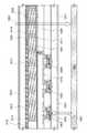
図8は、本発明のタッチパネルの構造を示す斜視図の一例である。図8に示すタッチパネルは、一対の基板間に液晶素子、フォトダイオード、薄膜トランジスタなどを含む画素が形成されたパネル1601と、第1の拡散板1602と、プリズムシート1603と、第2の拡散板1604と、導光板1605と、反射板1606と、複数の光源1607を有するバックライト1608と、回路基板1609とを有している。FIG. 8 is an example of a perspective view showing the structure of the touch panel of the present invention. 8 includes a
パネル1601と、第1の拡散板1602と、プリズムシート1603と、第2の拡散板1604と、導光板1605と、反射板1606とは、順に積層されている。光源1607は導光板1605の端部に設けられており、導光板1605内部に拡散された光源1607からの光は、第1の拡散板1602、プリズムシート1603及び第2の拡散板1604によって、対向基板側から均一にパネル1601に照射される。The
なお、本実施例では、第1の拡散板1602と第2の拡散板1604とを用いているが、拡散板の数はこれに限定されず、単数であっても3以上であっても良い。そして、拡散板は導光板1605とパネル1601の間に設けられていれば良い。よって、プリズムシート1603よりもパネル1601に近い側にのみ拡散板が設けられていても良いし、プリズムシート1603よりも導光板1605に近い側にのみ拡散板が設けられていても良い。In this embodiment, the
またプリズムシート1603は、図8に示した断面が鋸歯状の形状に限定されず、導光板1605からの光をパネル1601側に集光できる形状を有していれば良い。Further, the
回路基板1609には、パネル1601に入力される各種信号を生成もしくは処理する回路、パネル1601から出力される各種信号を処理する回路などが設けられている。そして図8では、回路基板1609とパネル1601とが、FPC(Flexible Printed Circuit)1611を介して接続されている。なお、上記回路は、COG(Chip ON Glass)法を用いてパネル1601に接続されていても良いし、上記回路の一部がFPC1611にCOF(Chip ON Film)法を用いて接続されていても良い。The
図8では、光源1607の駆動を制御する、制御系の回路が回路基板1609に設けられており、該制御系の回路と光源1607とがFPC1610を介して接続されている例を示している。ただし、上記制御系の回路はパネル1601に形成されていても良く、この場合はパネル1601と光源1607とがFPCなどにより接続されるようにする。FIG. 8 illustrates an example in which a circuit of a control system that controls driving of the
なお、図8は、パネル1601の端に光源1607を配置するエッジライト型の光源を例示しているが、本発明のタッチパネルは光源1607がパネル1601の直下に配置される直下型であっても良い。8 illustrates an edge light type light source in which the
例えば、被検出物である指1612をTFT基板側からパネル1601に近づけると、バックライト1608からの光が、パネル1601を通過し、その一部が指1612において反射し、再びパネル1601に入射する。各色に対応する光源1607を順に点灯させ、色ごとに撮像データの取得を行うことで、被検出物である指1612のカラーの撮像データを得ることが出来る。For example, when a
本実施例は、上記実施の形態と適宜組み合わせて実施することができる。This example can be implemented in combination with any of the above embodiments as appropriate.
本発明の一態様に係るタッチパネルは、高分解能である撮像データの取得を行うことができるという特徴を有している。よって、本発明の一態様に係るタッチパネルを用いた電子機器は、タッチパネルをその構成要素に追加することにより、より高機能のアプリケーションを搭載することができるようになる。本発明のタッチパネルは、表示装置、ノート型パーソナルコンピュータ、記録媒体を備えた画像再生装置(代表的にはDVD:Digital Versatile Disc等の記録媒体を再生し、その画像を表示しうるディスプレイを有する装置)に用いることができる。その他に、本発明の一態様に係るタッチパネルを用いることができる電子機器として、携帯電話、携帯型ゲーム機、携帯情報端末、電子書籍、ビデオカメラ、デジタルスチルカメラ等のカメラ、ゴーグル型ディスプレイ(ヘッドマウントディスプレイ)、ナビゲーションシステム、音響再生装置(カーオーディオ、デジタルオーディオプレイヤー等)、複写機、ファクシミリ、プリンター、プリンター複合機、現金自動預け入れ払い機(ATM)、自動販売機などが挙げられる。これら電子機器の具体例を図9に示す。The touch panel according to one embodiment of the present invention has a feature that imaging data with high resolution can be obtained. Therefore, an electronic device using the touch panel according to one embodiment of the present invention can be loaded with a higher-function application by adding the touch panel to its constituent elements. The touch panel of the present invention includes a display device, a notebook personal computer, and an image playback device including a recording medium (typically a device having a display that can play back a recording medium such as a DVD: Digital Versatile Disc and display the image. ). In addition, as an electronic device that can use the touch panel according to one embodiment of the present invention, a mobile phone, a portable game machine, a portable information terminal, an electronic book, a video camera, a digital still camera, or the like, a goggle-type display (head Mount display), navigation system, sound reproduction device (car audio, digital audio player, etc.), copying machine, facsimile, printer, printer multifunction device, automatic teller machine (ATM), vending machine, and the like. Specific examples of these electronic devices are shown in FIGS.
図9(A)は表示装置であり、筐体5001、表示部5002、支持台5003等を有する。本発明の一態様に係るタッチパネルは、表示部5002に用いることができる。表示部5002に本発明の一態様に係るタッチパネルを用いることで、高分解能である撮像データの取得を行うことができ、より高機能のアプリケーションが搭載された表示装置を提供することができる。なお、表示装置には、パーソナルコンピュータ用、TV放送受信用、広告表示用などの全ての情報表示用表示装置が含まれる。FIG. 9A illustrates a display device, which includes a housing 5001, a display portion 5002, a support base 5003, and the like. The touch panel according to one embodiment of the present invention can be used for the display portion 5002. By using the touch panel according to one embodiment of the present invention for the display portion 5002, imaging data with high resolution can be obtained, and a display device on which a higher-function application is mounted can be provided. The display device includes all information display devices for personal computers, TV broadcast reception, advertisement display, and the like.
図9(B)は携帯情報端末であり、筐体5101、表示部5102、スイッチ5103、操作キー5104、赤外線ポート5105等を有する。本発明の一態様に係るタッチパネルは、表示部5102に用いることができる。表示部5102に本発明の一態様に係るタッチパネルを用いることで、高分解能である撮像データの取得を行うことができ、より高機能のアプリケーションが搭載された携帯情報端末を提供することができる。FIG. 9B illustrates a portable information terminal, which includes a housing 5101, a display portion 5102, a switch 5103,
図9(C)は現金自動預け入れ払い機であり、筐体5201、表示部5202、硬貨投入口5203、紙幣投入口5204、カード投入口5205、通帳投入口5206等を有する。本発明の一態様に係るタッチパネルは、表示部5202に用いることができる。表示部5202に本発明の一態様に係るタッチパネルを用いることで、高分解能である撮像データの取得を行うことができ、より高機能のアプリケーションが搭載された現金自動預け入れ払い機を提供することができる。そして、本発明の一態様に係るタッチパネルを用いた現金自動預け入れ払い機は、指紋、顔、手形、掌紋及び手の静脈の形状、虹彩等の、生体認証に用いられる生体情報の読み取りを、より高精度で行うことが出来る。よって、生体認証における、本人であるにもかかわらず本人ではないと誤認識してしまう本人拒否率と、他人であるにもかかわらず本人と誤認識してしまう他人受入率とを、低く抑えることができる。FIG. 9C illustrates an automatic teller machine, which includes a housing 5201, a display portion 5202, a coin slot 5203, a bill slot 5204, a card slot 5205, a bankbook slot 5206, and the like. The touch panel according to one embodiment of the present invention can be used for the display portion 5202. By using the touch panel according to one embodiment of the present invention for the display portion 5202, it is possible to acquire imaging data with high resolution and provide an automatic teller machine with a higher-function application. it can. And the automatic teller machine using the touch panel according to one embodiment of the present invention is more capable of reading biometric information used for biometric authentication, such as fingerprints, faces, handprints, palm prints, hand vein shapes, irises, and the like. It can be performed with high accuracy. Therefore, in the biometric authentication, the identity rejection rate that misidentifies the person but not the identity, and the acceptance rate that misidentifies the identity but not the identity of the other person are kept low. Can do.
図9(D)は携帯型ゲーム機であり、筐体5301、筐体5302、表示部5303、表示部5304、マイクロホン5305、スピーカー5306、操作キー5307、スタイラス5308等を有する。本発明の一態様に係るタッチパネルは、表示部5303または表示部5304に用いることができる。表示部5303または表示部5304に本発明の一態様に係るタッチパネルを用いることで、高分解能である撮像データの取得を行うことができ、より高機能のアプリケーションが搭載された携帯型ゲーム機を提供することができる。なお、図9(D)に示した携帯型ゲーム機は、2つの表示部5303と表示部5304とを有しているが、携帯型ゲーム機が有する表示部の数は、これに限定されない。FIG. 9D illustrates a portable game machine including a housing 5301, a housing 5302, a display portion 5303, a display portion 5304, a microphone 5305, a speaker 5306, operation keys 5307, a stylus 5308, and the like. The touch panel according to one embodiment of the present invention can be used for the display portion 5303 or the display portion 5304. By using the touch panel according to one embodiment of the present invention for the display portion 5303 or the display portion 5304, imaging data with high resolution can be obtained, and a portable game machine equipped with a higher-function application is provided can do. Note that the portable game machine illustrated in FIG. 9D includes the two display portions 5303 and the display portion 5304; however, the number of display portions included in the portable game machine is not limited thereto.
図9(E)は電子黒板であり、筐体5401、描画部5402等を有する。電子黒板では、スタイラス5403または油性インクを用いたマーカーなどを用いて描画部5402に字または絵などの情報を書き込むことができる。さらに、電子黒板は、描画部5402に書き込まれた情報をフォトセンサにより電子データ化することができる。スタイラス5403を用いる場合、描画部5402に書き込まれた情報は、フォトセンサにより電子データ化された後、表示素子により描画部5402において表示される。本発明の一態様に係るタッチパネルは、描画部5402に用いることができる。描画部5402に本発明の一態様に係るタッチパネルを用いることで、高分解能である撮像データの取得を行うことができ、より高機能のアプリケーションが搭載された電子黒板を提供することができる。FIG. 9E illustrates an electronic blackboard which includes a housing 5401, a drawing portion 5402, and the like. In the electronic blackboard, information such as a character or a picture can be written in the drawing portion 5402 using a stylus 5403 or a marker using oil-based ink. Further, the electronic blackboard can convert information written in the drawing unit 5402 into electronic data using a photosensor. When the stylus 5403 is used, information written in the drawing unit 5402 is converted into electronic data by a photosensor and then displayed on the drawing unit 5402 by a display element. The touch panel according to one embodiment of the present invention can be used for the drawing portion 5402. By using the touch panel according to one embodiment of the present invention for the drawing portion 5402, imaging data with high resolution can be acquired, and an electronic blackboard equipped with a higher-function application can be provided.
本実施例は、上記実施の形態または上記実施例と適宜組み合わせて実施することが可能である。This example can be implemented in combination with any of the above embodiment modes or the above examples as appropriate.
100 タッチパネル
101 画素回路
102 表示素子制御回路
103 フォトセンサ制御回路
104 画素
105 表示素子
106 フォトセンサ
107 表示素子駆動回路
108 表示素子駆動回路
109 フォトセンサ読み出し回路
110 フォトセンサ駆動回路
201 トランジスタ
202 保持容量
203 液晶素子
204 フォトダイオード
205 トランジスタ
206 トランジスタ
207 ゲート信号線
208 フォトダイオードリセット信号線
209 ゲート信号線
210 ビデオデータ信号線
211 フォトセンサ出力信号線
212 フォトセンサ基準信号線
213 ゲート信号線
300 フォトセンサ読み出し回路
301 p型TFT
302 保持容量
303 プリチャージ信号線
401 信号
402 信号
403 信号
404 信号
405 信号
1001 基板
1002 フォトダイオード
1003 トランジスタ
1004 保持容量
1005 液晶素子
1006 半導体膜
1007 画素電極
1008 液晶
1009 対向電極
1010 導電膜
1011 配向膜
1012 配向膜
1013 基板
1014 カラーフィルタ
1015 遮蔽膜
1016 スペーサー
1017 偏光板
1018 偏光板
1020 矢印
1021 被検出物
1022 矢印
1601 パネル
1602 拡散板
1603 プリズムシート
1604 拡散板
1605 導光板
1606 反射板
1607 光源
1608 バックライト
1609 回路基板
1610 FPC
1611 FPC
1612 指
5001 筐体
5002 表示部
5003 支持台
5101 筐体
5102 表示部
5103 スイッチ
5104 操作キー
5105 赤外線ポート
5201 筐体
5202 表示部
5203 硬貨投入口
5204 紙幣投入口
5205 カード投入口
5206 通帳投入口
5301 筐体
5302 筐体
5303 表示部
5304 表示部
5305 マイクロホン
5306 スピーカー
5307 操作キー
5308 スタイラス
5401 筐体
5402 描画部
5403 スタイラスDESCRIPTION OF SYMBOLS 100
302
1611 FPC
1612 Finger 5001 Case 5002 Display unit 5003 Support base 5101 Case 5102 Display unit 5103
Claims (5)
Translated fromJapanese前記反射板上の、導光板と、A light guide plate on the reflector;
前記導光板上の、第1の拡散板と、A first diffusion plate on the light guide plate;
前記第1の拡散板上の、プリズムシートと、A prism sheet on the first diffusion plate;
前記プリズムシート上の、第2の拡散板と、A second diffusion plate on the prism sheet;
前記第2の拡散板上の、タッチセンサを有するパネルと、A panel having a touch sensor on the second diffusion plate;
前記導光板の端部側の、光源とを有し、A light source on an end side of the light guide plate;
前記タッチセンサを有するパネルは、The panel having the touch sensor is
第1の基板と、A first substrate;
第2の基板と、A second substrate;
前記第1の基板側の、第1のトランジスタ、及び前記第1のトランジスタと電気的に接続された画素電極と、A first transistor on the first substrate side and a pixel electrode electrically connected to the first transistor;
前記第1の基板側の、第2のトランジスタ、及び前記第2のトランジスタと電気的に接続されたフォトダイオードと、A second transistor on the first substrate side, and a photodiode electrically connected to the second transistor;
前記第2の基板側の、遮光膜、及びカラーフィルタとを有し、A light-shielding film and a color filter on the second substrate side;
前記第1のトランジスタと前記画素電極とを有する第1の領域は、前記カラーフィルタと重なる領域を有し、A first region having the first transistor and the pixel electrode has a region overlapping the color filter;
前記第2のトランジスタと前記フォトダイオードとを有する第2の領域は、前記遮光膜と重なる領域を有することを特徴とする表示装置。The display device, wherein the second region including the second transistor and the photodiode has a region overlapping with the light shielding film.
前記反射板上の、導光板と、A light guide plate on the reflector;
前記導光板上の、第1の拡散板と、A first diffusion plate on the light guide plate;
前記第1の拡散板上の、プリズムシートと、A prism sheet on the first diffusion plate;
前記プリズムシート上の、第2の拡散板と、A second diffusion plate on the prism sheet;
前記第2の拡散板上の、タッチセンサを有するパネルと、A panel having a touch sensor on the second diffusion plate;
前記導光板の端部側の、光源とを有し、A light source on an end side of the light guide plate;
前記タッチセンサを有するパネルは、The panel having the touch sensor is
第1の基板と、A first substrate;
第2の基板と、A second substrate;
前記第1の基板側の、第1のトランジスタ、及び前記第1のトランジスタと電気的に接続された画素電極と、A first transistor on the first substrate side and a pixel electrode electrically connected to the first transistor;
前記第1の基板側の、第2のトランジスタ、及び前記第2のトランジスタと電気的に接続されたフォトダイオードと、A second transistor on the first substrate side, and a photodiode electrically connected to the second transistor;
前記第2の基板側の、遮光膜、及びカラーフィルタとを有し、A light-shielding film and a color filter on the second substrate side;
前記カラーフィルタは、前記画素電極と重なる領域を有し、The color filter has a region overlapping with the pixel electrode,
前記遮光膜は、前記フォトダイオードと重なる領域を有することを特徴とする表示装置。The display device, wherein the light shielding film has a region overlapping with the photodiode.
前記第1の基板と、前記第2の基板との間にスペーサを有し、A spacer between the first substrate and the second substrate;
前記スペーサは、前記遮光膜と重なる領域を有することを特徴とする表示装置。The display device, wherein the spacer has a region overlapping with the light shielding film.
前記プリズムシートは、鋸歯の形状を有することを特徴とする表示装置。The display device, wherein the prism sheet has a sawtooth shape.
前記光源は、白色光を呈することを特徴とする表示装置。The display device, wherein the light source exhibits white light.
Priority Applications (1)
| Application Number | Priority Date | Filing Date | Title |
|---|---|---|---|
| JP2010151515AJP5459910B2 (en) | 2009-07-02 | 2010-07-02 | Display device |
Applications Claiming Priority (3)
| Application Number | Priority Date | Filing Date | Title |
|---|---|---|---|
| JP2009157474 | 2009-07-02 | ||
| JP2009157474 | 2009-07-02 | ||
| JP2010151515AJP5459910B2 (en) | 2009-07-02 | 2010-07-02 | Display device |
Related Child Applications (1)
| Application Number | Title | Priority Date | Filing Date |
|---|---|---|---|
| JP2013253220ADivisionJP5771262B2 (en) | 2009-07-02 | 2013-12-06 | Display device |
Publications (3)
| Publication Number | Publication Date |
|---|---|
| JP2011028744A JP2011028744A (en) | 2011-02-10 |
| JP2011028744A5 JP2011028744A5 (en) | 2013-08-01 |
| JP5459910B2true JP5459910B2 (en) | 2014-04-02 |
Family
ID=43412386
Family Applications (2)
| Application Number | Title | Priority Date | Filing Date |
|---|---|---|---|
| JP2010151515AExpired - Fee RelatedJP5459910B2 (en) | 2009-07-02 | 2010-07-02 | Display device |
| JP2013253220AExpired - Fee RelatedJP5771262B2 (en) | 2009-07-02 | 2013-12-06 | Display device |
Family Applications After (1)
| Application Number | Title | Priority Date | Filing Date |
|---|---|---|---|
| JP2013253220AExpired - Fee RelatedJP5771262B2 (en) | 2009-07-02 | 2013-12-06 | Display device |
Country Status (4)
| Country | Link |
|---|---|
| US (1) | US20110001725A1 (en) |
| JP (2) | JP5459910B2 (en) |
| KR (1) | KR101703510B1 (en) |
| TW (2) | TWI547845B (en) |
Families Citing this family (37)
| Publication number | Priority date | Publication date | Assignee | Title |
|---|---|---|---|---|
| US8624875B2 (en)* | 2009-08-24 | 2014-01-07 | Semiconductor Energy Laboratory Co., Ltd. | Method for driving touch panel |
| US8907881B2 (en) | 2010-04-09 | 2014-12-09 | Semiconductor Energy Laboratory Co., Ltd. | Liquid crystal display device and method for driving the same |
| WO2011125688A1 (en) | 2010-04-09 | 2011-10-13 | Semiconductor Energy Laboratory Co., Ltd. | Liquid crystal display device and method for driving the same |
| US8537086B2 (en) | 2010-06-16 | 2013-09-17 | Semiconductor Energy Laboratory Co., Ltd. | Driving method of liquid crystal display device |
| JP5823740B2 (en)* | 2010-06-16 | 2015-11-25 | 株式会社半導体エネルギー研究所 | Input/Output Devices |
| WO2011158948A1 (en) | 2010-06-18 | 2011-12-22 | Semiconductor Energy Laboratory Co., Ltd. | Method of manufacturing power storage device |
| US8564529B2 (en) | 2010-06-21 | 2013-10-22 | Semiconductor Energy Laboratory Co., Ltd. | Method for driving liquid crystal display device |
| KR20130116857A (en) | 2010-06-25 | 2013-10-24 | 가부시키가이샤 한도오따이 에네루기 켄큐쇼 | Liquid crystal display device and electronic appliance |
| US9286848B2 (en) | 2010-07-01 | 2016-03-15 | Semiconductor Energy Laboratory Co., Ltd. | Method for driving liquid crystal display device |
| US9064469B2 (en) | 2010-07-02 | 2015-06-23 | Semiconductor Energy Laboratory Co., Ltd. | Method for driving liquid crystal display device |
| US8988337B2 (en) | 2010-07-02 | 2015-03-24 | Semiconductor Energy Laboratory Co., Ltd. | Driving method of liquid crystal display device |
| CN102971784B (en) | 2010-07-02 | 2016-08-03 | 株式会社半导体能源研究所 | Liquid crystal display device and method of driving liquid crystal display device |
| JP2012048220A (en) | 2010-07-26 | 2012-03-08 | Semiconductor Energy Lab Co Ltd | Liquid crystal display device and its driving method |
| WO2012014686A1 (en) | 2010-07-27 | 2012-02-02 | Semiconductor Energy Laboratory Co., Ltd. | Method for driving liquid crystal display device |
| TWI562109B (en) | 2010-08-05 | 2016-12-11 | Semiconductor Energy Lab Co Ltd | Driving method of liquid crystal display device |
| US8643580B2 (en) | 2010-08-31 | 2014-02-04 | Semiconductor Energy Laboratory Co., Ltd. | Method for driving liquid crystal display device |
| JP2012103683A (en) | 2010-10-14 | 2012-05-31 | Semiconductor Energy Lab Co Ltd | Display device and driving method for the same |
| DE102011011767A1 (en)* | 2011-02-18 | 2012-08-23 | Fresenius Medical Care Deutschland Gmbh | Medical device with multi-function display |
| CN103890947B (en) | 2011-10-28 | 2017-04-12 | 株式会社半导体能源研究所 | Imaging device |
| CN103176636A (en)* | 2011-12-26 | 2013-06-26 | 富泰华工业(深圳)有限公司 | Touch screen and display device thereof |
| CN103325339B (en)* | 2013-06-21 | 2016-05-25 | 京东方科技集团股份有限公司 | Image element circuit and driving method thereof, organic electroluminescence display panel and display unit |
| US9455281B2 (en) | 2014-06-19 | 2016-09-27 | Semiconductor Energy Laboratory Co., Ltd. | Touch sensor, touch panel, touch panel module, and display device |
| TWI651567B (en) | 2015-07-03 | 2019-02-21 | 友達光電股份有限公司 | Display and manufacturing method thereof |
| KR102586792B1 (en)* | 2016-08-23 | 2023-10-12 | 삼성디스플레이 주식회사 | Display device and driving method thereof |
| CN107293553B (en)* | 2017-06-19 | 2020-11-24 | 京东方科技集团股份有限公司 | Array substrate and preparation method thereof, display panel and display device |
| CN109254677A (en)* | 2017-07-13 | 2019-01-22 | 群创光电股份有限公司 | Display device and method for sensing touch signal using the same |
| TWI620109B (en)* | 2017-12-06 | 2018-04-01 | 友達光電股份有限公司 | Touch display panel |
| US11257457B2 (en) | 2018-02-23 | 2022-02-22 | Semiconductor Energy Laboratory Co., Ltd. | Display device and operation method thereof |
| JP7478097B2 (en) | 2018-09-14 | 2024-05-02 | 株式会社半導体エネルギー研究所 | Display device |
| US12048227B2 (en) | 2019-02-15 | 2024-07-23 | Semiconductor Energy Laboratory Co., Ltd. | Display device, display module, and electronic device |
| JP7300869B2 (en)* | 2019-04-02 | 2023-06-30 | 株式会社ジャパンディスプレイ | Biometric authentication system and biometric information detection device |
| CN110061042B (en)* | 2019-04-29 | 2021-02-02 | 上海天马微电子有限公司 | Display panel and display device |
| CN110299106B (en)* | 2019-06-27 | 2020-11-27 | 上海天马有机发光显示技术有限公司 | Light sensing driving circuit, driving method thereof and display device |
| US11301708B2 (en)* | 2019-10-01 | 2022-04-12 | Novatek Microelectronics Corp. | Image sensing circuit and method |
| JP7510432B2 (en) | 2019-10-11 | 2024-07-03 | 株式会社半導体エネルギー研究所 | Display device, display module, and electronic device |
| US11244974B2 (en)* | 2020-03-30 | 2022-02-08 | Novatek Microelectronics Corp. | Image sensing system |
| CN112083593B (en)* | 2020-09-29 | 2021-12-03 | Tcl华星光电技术有限公司 | Display panel and display device |
Family Cites Families (53)
| Publication number | Priority date | Publication date | Assignee | Title |
|---|---|---|---|---|
| JPS631936A (en)* | 1986-06-23 | 1988-01-06 | Asahi Optical Co Ltd | Photoelectric conversion circuit |
| US5313055A (en)* | 1991-09-30 | 1994-05-17 | Fuji Xerox Co., Ltd. | Two-dimensional image read/display device |
| JP2784615B2 (en)* | 1991-10-16 | 1998-08-06 | 株式会社半導体エネルギー研究所 | Electro-optical display device and driving method thereof |
| US7253440B1 (en)* | 1991-10-16 | 2007-08-07 | Semiconductor Energy Laboratory Co., Ltd. | Semiconductor device having at least first and second thin film transistors |
| US6759680B1 (en)* | 1991-10-16 | 2004-07-06 | Semiconductor Energy Laboratory Co., Ltd. | Display device having thin film transistors |
| US7071910B1 (en)* | 1991-10-16 | 2006-07-04 | Semiconductor Energy Laboratory Co., Ltd. | Electrooptical device and method of driving and manufacturing the same |
| GB9209734D0 (en)* | 1992-05-06 | 1992-06-17 | Philips Electronics Uk Ltd | An image sensor |
| JP3139134B2 (en)* | 1992-06-03 | 2001-02-26 | カシオ計算機株式会社 | Liquid crystal display |
| US5501989A (en)* | 1993-03-22 | 1996-03-26 | Semiconductor Energy Laboratory Co., Ltd. | Method of making semiconductor device/circuit having at least partially crystallized semiconductor layer |
| DE69321822T2 (en)* | 1993-05-19 | 1999-04-01 | Hewlett-Packard Gmbh, 71034 Boeblingen | Photodiode structure |
| JP2821347B2 (en)* | 1993-10-12 | 1998-11-05 | 日本電気株式会社 | Current control type light emitting element array |
| JPH07130974A (en)* | 1993-11-02 | 1995-05-19 | Semiconductor Energy Lab Co Ltd | Semiconductor device and operating method thereof |
| JPH07236029A (en)* | 1993-12-29 | 1995-09-05 | Xerox Corp | Compact document imager |
| US5627364A (en)* | 1994-10-11 | 1997-05-06 | Tdk Corporation | Linear array image sensor with thin-film light emission element light source |
| US5625210A (en)* | 1995-04-13 | 1997-04-29 | Eastman Kodak Company | Active pixel sensor integrated with a pinned photodiode |
| JPH09138390A (en)* | 1995-09-14 | 1997-05-27 | Canon Inc | Liquid crystal display |
| JP3436629B2 (en)* | 1996-01-08 | 2003-08-11 | シャープ株式会社 | Apparatus for display and imaging |
| JP3008859B2 (en)* | 1996-09-18 | 2000-02-14 | 日本電気株式会社 | Image sensor device using thin light source |
| US6188380B1 (en)* | 1997-02-03 | 2001-02-13 | Nanao Corporation | Photodetector of liquid crystal display and luminance control device using the same |
| JP3641342B2 (en)* | 1997-03-07 | 2005-04-20 | Tdk株式会社 | Semiconductor device and organic EL display device |
| US6518962B2 (en)* | 1997-03-12 | 2003-02-11 | Seiko Epson Corporation | Pixel circuit display apparatus and electronic apparatus equipped with current driving type light-emitting device |
| EP0915367B1 (en)* | 1997-04-22 | 2007-06-06 | Matsushita Electric Industrial Co., Ltd. | Liquid crystal display with image reading function, image reading method and manufacturing method |
| JP4318768B2 (en)* | 1997-07-23 | 2009-08-26 | 株式会社半導体エネルギー研究所 | Method for manufacturing semiconductor device |
| JP4013293B2 (en)* | 1997-09-01 | 2007-11-28 | セイコーエプソン株式会社 | Display device combined type image sensor device and active matrix display device |
| JP4271268B2 (en)* | 1997-09-20 | 2009-06-03 | 株式会社半導体エネルギー研究所 | Image sensor and image sensor integrated active matrix display device |
| JP4044187B2 (en)* | 1997-10-20 | 2008-02-06 | 株式会社半導体エネルギー研究所 | Active matrix display device and manufacturing method thereof |
| JP3031332B2 (en)* | 1998-05-06 | 2000-04-10 | 日本電気株式会社 | Image sensor |
| US6476864B1 (en)* | 1998-05-11 | 2002-11-05 | Agilent Technologies, Inc. | Pixel sensor column amplifier architecture |
| JP4164910B2 (en)* | 1998-09-21 | 2008-10-15 | ソニー株式会社 | Organic EL display and organic EL display manufacturing method |
| US6480305B1 (en)* | 1999-05-25 | 2002-11-12 | Hewlett-Packard Company | Imaging device |
| JP2001075524A (en)* | 1999-09-03 | 2001-03-23 | Rohm Co Ltd | Display device |
| US6392617B1 (en)* | 1999-10-27 | 2002-05-21 | Agilent Technologies, Inc. | Active matrix light emitting diode display |
| US6747638B2 (en)* | 2000-01-31 | 2004-06-08 | Semiconductor Energy Laboratory Co., Ltd. | Adhesion type area sensor and display device having adhesion type area sensor |
| JP4112184B2 (en) | 2000-01-31 | 2008-07-02 | 株式会社半導体エネルギー研究所 | Area sensor and display device |
| US7751600B2 (en)* | 2000-04-18 | 2010-07-06 | Semiconductor Energy Laboratory Co., Ltd. | System and method for identifying an individual |
| JP4364452B2 (en) | 2000-05-09 | 2009-11-18 | 株式会社半導体エネルギー研究所 | Portable information communication device |
| KR100771258B1 (en)* | 2000-05-09 | 2007-10-29 | 가부시키가이샤 한도오따이 에네루기 켄큐쇼 | Identity verification system, identity verification method and mobile phone device |
| US7030551B2 (en)* | 2000-08-10 | 2006-04-18 | Semiconductor Energy Laboratory Co., Ltd. | Area sensor and display apparatus provided with an area sensor |
| JP4703883B2 (en)* | 2001-04-09 | 2011-06-15 | 株式会社半導体エネルギー研究所 | Method for manufacturing semiconductor device |
| JP2002319679A (en)* | 2001-04-20 | 2002-10-31 | Semiconductor Energy Lab Co Ltd | Semiconductor device |
| JP2004140338A (en)* | 2002-09-26 | 2004-05-13 | Toshiba Matsushita Display Technology Co Ltd | Optical sensor element and manufacturing method therefor, and flat display device using the optical sensor element and manufacturing method therefor |
| JP2006079589A (en)* | 2004-08-05 | 2006-03-23 | Sanyo Electric Co Ltd | Touch panel |
| US7365494B2 (en)* | 2004-12-03 | 2008-04-29 | Semiconductor Energy Laboratory Co., Ltd. | Display device and manufacturing method thereof |
| JP4678852B2 (en)* | 2005-11-29 | 2011-04-27 | キヤノン株式会社 | Optical information recording / reproducing apparatus and element used therefor |
| JP2007183706A (en) | 2006-01-04 | 2007-07-19 | Epson Imaging Devices Corp | Touch sensor system |
| JP4867766B2 (en)* | 2007-04-05 | 2012-02-01 | セイコーエプソン株式会社 | Liquid crystal device, image sensor, and electronic device |
| WO2008143211A1 (en)* | 2007-05-18 | 2008-11-27 | Sharp Kabushiki Kaisha | Display device |
| TWI347453B (en)* | 2007-06-23 | 2011-08-21 | Ind Tech Res Inst | Hybrid multiplexed 3d display and a displaying method thereof |
| JP5176434B2 (en)* | 2007-08-28 | 2013-04-03 | セイコーエプソン株式会社 | Electro-optical device and electronic apparatus |
| US20090141004A1 (en)* | 2007-12-03 | 2009-06-04 | Semiconductor Energy Laboratory Co., Ltd. | Display device and method for manufacturing the same |
| CN101911159A (en)* | 2008-03-03 | 2010-12-08 | 夏普株式会社 | Display device with light sensors |
| US8319750B2 (en)* | 2008-05-02 | 2012-11-27 | Sony Corporation | Sensing circuit, method of driving sensing circuit, display device, method of driving display device, and electronic apparatus |
| CN100590581C (en)* | 2008-05-21 | 2010-02-17 | 友达光电股份有限公司 | Touch panel and portable electronic device with same |
- 2010
- 2010-06-30TWTW104116467Apatent/TWI547845B/ennot_activeIP Right Cessation
- 2010-06-30TWTW099121504Apatent/TWI496042B/ennot_activeIP Right Cessation
- 2010-07-01USUS12/828,910patent/US20110001725A1/ennot_activeAbandoned
- 2010-07-01KRKR1020100063293Apatent/KR101703510B1/ennot_activeExpired - Fee Related
- 2010-07-02JPJP2010151515Apatent/JP5459910B2/ennot_activeExpired - Fee Related
- 2013
- 2013-12-06JPJP2013253220Apatent/JP5771262B2/ennot_activeExpired - Fee Related
Also Published As
| Publication number | Publication date |
|---|---|
| JP5771262B2 (en) | 2015-08-26 |
| JP2011028744A (en) | 2011-02-10 |
| US20110001725A1 (en) | 2011-01-06 |
| TWI547845B (en) | 2016-09-01 |
| TWI496042B (en) | 2015-08-11 |
| KR101703510B1 (en) | 2017-02-07 |
| TW201533502A (en) | 2015-09-01 |
| JP2014063521A (en) | 2014-04-10 |
| TW201117074A (en) | 2011-05-16 |
| KR20110002812A (en) | 2011-01-10 |
Similar Documents
| Publication | Publication Date | Title |
|---|---|---|
| JP5459910B2 (en) | Display device | |
| JP6117836B2 (en) | Display device | |
| JP5513307B2 (en) | Touch panel drive method | |
| JP5679530B2 (en) | Electronics | |
| JP5791753B2 (en) | Display device with touch panel | |
| JP5866089B2 (en) | Electronics | |
| JP5913517B2 (en) | Semiconductor device |
Legal Events
| Date | Code | Title | Description |
|---|---|---|---|
| A521 | Request for written amendment filed | Free format text:JAPANESE INTERMEDIATE CODE: A523 Effective date:20130619 | |
| A621 | Written request for application examination | Free format text:JAPANESE INTERMEDIATE CODE: A621 Effective date:20130619 | |
| A977 | Report on retrieval | Free format text:JAPANESE INTERMEDIATE CODE: A971007 Effective date:20131023 | |
| A131 | Notification of reasons for refusal | Free format text:JAPANESE INTERMEDIATE CODE: A131 Effective date:20131029 | |
| A521 | Request for written amendment filed | Free format text:JAPANESE INTERMEDIATE CODE: A523 Effective date:20131206 | |
| TRDD | Decision of grant or rejection written | ||
| A01 | Written decision to grant a patent or to grant a registration (utility model) | Free format text:JAPANESE INTERMEDIATE CODE: A01 Effective date:20140107 | |
| A61 | First payment of annual fees (during grant procedure) | Free format text:JAPANESE INTERMEDIATE CODE: A61 Effective date:20140113 | |
| R150 | Certificate of patent or registration of utility model | Free format text:JAPANESE INTERMEDIATE CODE: R150 Ref document number:5459910 Country of ref document:JP Free format text:JAPANESE INTERMEDIATE CODE: R150 | |
| R250 | Receipt of annual fees | Free format text:JAPANESE INTERMEDIATE CODE: R250 | |
| R250 | Receipt of annual fees | Free format text:JAPANESE INTERMEDIATE CODE: R250 | |
| R250 | Receipt of annual fees | Free format text:JAPANESE INTERMEDIATE CODE: R250 | |
| R250 | Receipt of annual fees | Free format text:JAPANESE INTERMEDIATE CODE: R250 | |
| R250 | Receipt of annual fees | Free format text:JAPANESE INTERMEDIATE CODE: R250 | |
| R250 | Receipt of annual fees | Free format text:JAPANESE INTERMEDIATE CODE: R250 | |
| LAPS | Cancellation because of no payment of annual fees |