JP5458556B2 - Timing adjustment circuit, solid-state imaging device, and camera system - Google Patents
Timing adjustment circuit, solid-state imaging device, and camera systemDownload PDFInfo
- Publication number
- JP5458556B2 JP5458556B2JP2008303070AJP2008303070AJP5458556B2JP 5458556 B2JP5458556 B2JP 5458556B2JP 2008303070 AJP2008303070 AJP 2008303070AJP 2008303070 AJP2008303070 AJP 2008303070AJP 5458556 B2JP5458556 B2JP 5458556B2
- Authority
- JP
- Japan
- Prior art keywords
- delay
- circuit
- current
- delay element
- signal
- Prior art date
- Legal status (The legal status is an assumption and is not a legal conclusion. Google has not performed a legal analysis and makes no representation as to the accuracy of the status listed.)
- Expired - Fee Related
Links
Images


Classifications
- H—ELECTRICITY
- H03—ELECTRONIC CIRCUITRY
- H03L—AUTOMATIC CONTROL, STARTING, SYNCHRONISATION OR STABILISATION OF GENERATORS OF ELECTRONIC OSCILLATIONS OR PULSES
- H03L7/00—Automatic control of frequency or phase; Synchronisation
- H03L7/06—Automatic control of frequency or phase; Synchronisation using a reference signal applied to a frequency- or phase-locked loop
- H03L7/08—Details of the phase-locked loop
- H03L7/0805—Details of the phase-locked loop the loop being adapted to provide an additional control signal for use outside the loop
- H—ELECTRICITY
- H10—SEMICONDUCTOR DEVICES; ELECTRIC SOLID-STATE DEVICES NOT OTHERWISE PROVIDED FOR
- H10F—INORGANIC SEMICONDUCTOR DEVICES SENSITIVE TO INFRARED RADIATION, LIGHT, ELECTROMAGNETIC RADIATION OF SHORTER WAVELENGTH OR CORPUSCULAR RADIATION
- H10F39/00—Integrated devices, or assemblies of multiple devices, comprising at least one element covered by group H10F30/00, e.g. radiation detectors comprising photodiode arrays
- H10F39/80—Constructional details of image sensors
- H10F39/803—Pixels having integrated switching, control, storage or amplification elements
- H—ELECTRICITY
- H03—ELECTRONIC CIRCUITRY
- H03L—AUTOMATIC CONTROL, STARTING, SYNCHRONISATION OR STABILISATION OF GENERATORS OF ELECTRONIC OSCILLATIONS OR PULSES
- H03L7/00—Automatic control of frequency or phase; Synchronisation
- H03L7/06—Automatic control of frequency or phase; Synchronisation using a reference signal applied to a frequency- or phase-locked loop
- H03L7/08—Details of the phase-locked loop
- H03L7/099—Details of the phase-locked loop concerning mainly the controlled oscillator of the loop
- H03L7/0995—Details of the phase-locked loop concerning mainly the controlled oscillator of the loop the oscillator comprising a ring oscillator
- H—ELECTRICITY
- H03—ELECTRONIC CIRCUITRY
- H03L—AUTOMATIC CONTROL, STARTING, SYNCHRONISATION OR STABILISATION OF GENERATORS OF ELECTRONIC OSCILLATIONS OR PULSES
- H03L7/00—Automatic control of frequency or phase; Synchronisation
- H03L7/06—Automatic control of frequency or phase; Synchronisation using a reference signal applied to a frequency- or phase-locked loop
- H03L7/16—Indirect frequency synthesis, i.e. generating a desired one of a number of predetermined frequencies using a frequency- or phase-locked loop
- H03L7/18—Indirect frequency synthesis, i.e. generating a desired one of a number of predetermined frequencies using a frequency- or phase-locked loop using a frequency divider or counter in the loop
- H03L7/183—Indirect frequency synthesis, i.e. generating a desired one of a number of predetermined frequencies using a frequency- or phase-locked loop using a frequency divider or counter in the loop a time difference being used for locking the loop, the counter counting between fixed numbers or the frequency divider dividing by a fixed number
- H—ELECTRICITY
- H04—ELECTRIC COMMUNICATION TECHNIQUE
- H04L—TRANSMISSION OF DIGITAL INFORMATION, e.g. TELEGRAPHIC COMMUNICATION
- H04L7/00—Arrangements for synchronising receiver with transmitter
- H04L7/0008—Synchronisation information channels, e.g. clock distribution lines
- H04L7/0012—Synchronisation information channels, e.g. clock distribution lines by comparing receiver clock with transmitter clock
- H—ELECTRICITY
- H04—ELECTRIC COMMUNICATION TECHNIQUE
- H04L—TRANSMISSION OF DIGITAL INFORMATION, e.g. TELEGRAPHIC COMMUNICATION
- H04L7/00—Arrangements for synchronising receiver with transmitter
- H04L7/0016—Arrangements for synchronising receiver with transmitter correction of synchronization errors
- H04L7/0033—Correction by delay
- H04L7/0041—Delay of data signal
Landscapes
- Engineering & Computer Science (AREA)
- Computer Networks & Wireless Communication (AREA)
- Signal Processing (AREA)
- Transforming Light Signals Into Electric Signals (AREA)
- Pulse Circuits (AREA)
- Stabilization Of Oscillater, Synchronisation, Frequency Synthesizers (AREA)
Description
Translated fromJapanese本発明は、CMOSイメージセンサに代表されるタイミング調整回路、固体撮像素子、およびカメラシステムに関するものである。 The present invention relates to a timing adjustment circuit represented by a CMOS image sensor, a solid-state imaging device, and a camera system.
近年デジタルスチルカメラやカムコーダ、監視カメラ等の用途に、CCD(Charge Coupled Device)の他にCMOS(Complementary Metal Oxide Semiconductor)イメージセンサが広く使われるようになり、市場も拡大している。
CMOSイメージセンサは、各画素に入射した光を光電変換素子であるフォトダイオードで電子に変換し、それを一定期間蓄積した上で、その蓄積電荷量を反映した信号をデジタル化して外部のDSP等に出力する。In recent years, in addition to CCD (Charge Coupled Device), CMOS (Complementary Metal Oxide Semiconductor) image sensors have been widely used for applications such as digital still cameras, camcorders, and surveillance cameras, and the market is expanding.
A CMOS image sensor converts light incident on each pixel into electrons with a photodiode that is a photoelectric conversion element, accumulates the light for a certain period, digitizes a signal reflecting the amount of accumulated charge, and outputs an external DSP or the like. Output to.
一般的に、外部とのタイミング調整には、配線負荷などにより発生する外部インタフェースの遅延時間を制御し、内部クロックとの同期を調整するDLL(Delay Locked Loop)回路が用いられる。
ところが、イメージセンサでは、多画素化の要求を受けて、画素以外の周辺回路は小型化する必要があり、各データライン毎にDLLを搭載するのは困難である。Generally, for timing adjustment with the outside, a DLL (Delay Locked Loop) circuit that controls the delay time of the external interface generated by a wiring load and adjusts the synchronization with the internal clock is used.
However, in response to a request for increasing the number of pixels in an image sensor, it is necessary to downsize peripheral circuits other than pixels, and it is difficult to mount a DLL for each data line.
特許文献1の技術を応用した遅延回路が提案されている。
この遅延回路では、PLL(Phase Locked Loop)を用いて精度の高い遅延時間を作り出し、それを各データラインに設置された遅延回路に供給する。
この遅延回路においては、遅延時間の制御はPLLの発振周波数を制御することで可能となる。この方式はPLL内部の発振器を遅延回路として用いることで、小型で精度の高い遅延回路の実現を可能にしている。A delay circuit applying the technique of
In this delay circuit, a highly accurate delay time is generated using a PLL (Phase Locked Loop), and the delay time is supplied to a delay circuit installed in each data line.
In this delay circuit, the delay time can be controlled by controlling the oscillation frequency of the PLL. In this system, a small and highly accurate delay circuit can be realized by using an internal oscillator as a delay circuit.
また、特許文献2には、データライン毎に遅延時間調節を可能としたワイドレンジクロック発生器が提案されている。
しかし、上記した特許文献1に開示された技術を応用した回路では、各データライン毎に配置された遅延回路にはすべて共通のコントロール電圧が供給されているため、各データライン毎に独立した遅延時間の調節はできない。 However, in the circuit to which the technique disclosed in
特許文献2に開示された技術では、データライン毎に遅延時間調節を可能としているが、調節幅はPLLの発振周波数に依存するため、高精度のタイミング調整のためにはPLLを高周波で発振させる必要がある。
一例として、最小遅延時間を50psとした場合、PLLは5GHzで発振する必要があり、このようなPLLは現実的に設計困難である。In the technique disclosed in
As an example, when the minimum delay time is 50 ps, the PLL needs to oscillate at 5 GHz, and such a PLL is practically difficult to design.
本発明は、データライン毎に独立した遅延時間の調節が可能で、しかも内蔵するPLLの発振周波数に依存することなく、遅延時間を調節することが可能なタイミング調整回路、固体撮像素子、およびカメラシステムを提供することにある。 The present invention provides a timing adjustment circuit, a solid-state imaging device, and a camera that can adjust the delay time independently for each data line and can adjust the delay time without depending on the oscillation frequency of the built-in PLL. To provide a system.
本発明の第1の観点のタイミング調整回路は、複数のデータラインと、発振信号を発振する複数の発振遅延素子を有し、基準クロックとフィードバッククロックとを位相同期させて上記発振信号を発振する位相同期回路と、上記データラインに配置された上記発振遅延素子と等価な遅延素子を含み、当該データラインを伝搬されるデータを遅延させる、上記複数のデータラインにそれぞれ配置された複数の遅延回路と、上記遅延回路ごとに独立して配置され、上記位相同期回路の発振にかかわる信号に応じて対応する上記遅延回路の遅延素子の遅延量を調節する複数の遅延調節部と、を有し、上記位相同期回路は、基準クロックとフィードバッククロックとの位相比較結果に応じた電圧を受けて、カレントミラー回路により得られた電流を上記発振遅延素子の電流源に供給して発振動作を行う電圧制御発振器を含み、上記遅延調節部は、上記位相同期回路のカレントミラー回路により得られた上記電流に応じた電流を、少なくとも一つのカレントミラー回路を介して対応する上記遅延回路の上記遅延素子の遅延量を調節する調節信号として当該遅延素子の電流源に供給する。A timing adjustment circuit according to a first aspect of the present invention includes aplurality of data lines and a plurality of oscillation delay elements that oscillate an oscillation signal, and oscillates the oscillation signal by synchronizing the phase of a reference clock and a feedback clock.A plurality of delay circuitsrespectively disposed on the plurality of data lines, each including a phase synchronization circuit and a delay element equivalent to the oscillation delay element disposed on the data line, and delaying data propagated throughthe data line; Whendisposed independently for each of the delay circuits,havea, aplurality of delay adjusting unit for adjusting the delay amount of the delay elements of saidcorresponding delay circuit in accordancewith a signal relating to the oscillation of the phase locked loopcircuit, The phase synchronization circuit receives a voltage corresponding to the phase comparison result between the reference clock and the feedback clock, and increases the current obtained by the current mirror circuit. A voltage-controlled oscillator that supplies a current source of an oscillation delay element to perform an oscillation operation, wherein the delay adjustment unit supplies at least one current corresponding to the current obtained by the current mirror circuit of the phase synchronization circuit. The signal is supplied to the current source of the delay element as an adjustment signal for adjusting the delay amount of the delay element of the corresponding delay circuit via a mirror circuit .
本発明の第2の観点の固体撮像素子は、光電変換を行う複数の画素が行列状に配列された画素部と、上記画素部から画素信号の読み出しを行い、読み出したアナログ画素信号をデジタル信号に変換する機能を含む画素読み出し部と、上記画素読み出し部によるデジタル信号の遅延タイミングを調整可能なタイミング調整回路と、を有し、上記タイミング調整回路は、複数のデータラインと、発振信号を発振する複数の発振遅延素子を有し、基準クロックとフィードバッククロックとを位相同期させて上記発振信号を発振する位相同期回路と、上記データラインに配置された上記発振遅延素子と等価な遅延素子を含み、当該データラインを伝搬されるデータを遅延させる、上記複数のデータラインにそれぞれ配置された複数の遅延回路と、上記遅延回路ごとに独立して配置され、上記位相同期回路の発振にかかわる信号に応じて対応する上記遅延回路の遅延素子の遅延量を調節する複数の遅延調節部と、を有し、上記位相同期回路は、基準クロックとフィードバッククロックとの位相比較結果に応じた電圧を受けて、カレントミラー回路により得られた電流を上記発振遅延素子の電流源に供給して発振動作を行う電圧制御発振器を含み、上記遅延調節部は、上記位相同期回路のカレントミラー回路により得られた上記電流に応じた電流を、少なくとも一つのカレントミラー回路を介して対応する上記遅延回路の上記遅延素子の遅延量を調節する調節信号として当該遅延素子の電流源に供給する。A solid-state imaging device according to a second aspect of the present invention includes a pixel unit in which a plurality of pixels that perform photoelectric conversion are arranged in a matrix, a pixel signal is read from the pixel unit, and the read analog pixel signal is converted into a digital signal. And a timing adjustment circuit capable of adjusting a delay timing of a digital signal by the pixel readout unit, and the timing adjustment circuit oscillates aplurality of data lines and an oscillation signal. A phase synchronization circuit that oscillates the oscillation signal by synchronizing the phase of a reference clock and a feedback clock, and a delay element equivalent to the oscillation delay element disposed on the data line. delays the data to be propagated through the data line, anda plurality of delay circuitswhich are respectively disposed on said plurality of data lines,the Are arranged independently for each extension circuit,havea, aplurality of delay adjusting unit for adjusting the delay amount of the delay elements of saidcorresponding delay circuit in accordancewith a signal relating to the oscillation of the phase synchronizingcircuit, the phase locked The circuit includes a voltage controlled oscillator that receives a voltage corresponding to a phase comparison result between the reference clock and the feedback clock, and supplies a current obtained by the current mirror circuit to the current source of the oscillation delay element to perform an oscillation operation. The delay adjustment unit adjusts the delay amount of the delay element of the delay circuit corresponding to the current corresponding to the current obtained by the current mirror circuit of the phase synchronization circuit via at least one current mirror circuit. The adjustment signal is supplied to the current source of the delay element .
本発明の第3の観点のカメラシステムは、固体撮像素子と、上記固体撮像素子に被写体像を結像する光学系と、上記固体撮像素子の出力画像信号を処理する信号処理回路と、を有し、上記固体撮像素子は、光電変換を行う複数の画素が行列状に配列された画素部と、上記画素部から画素信号の読み出しを行い、読み出したアナログ画素信号をデジタル信号に変換する機能を含む画素読み出し部と、上記画素読み出し部によるデジタル信号の遅延タイミングを調整可能なタイミング調整回路と、を有し、上記タイミング調整回路は、複数のデータラインと、発振信号を発振する複数の発振遅延素子を有し、基準クロックとフィードバッククロックとを位相同期させて上記発振信号を発振する位相同期回路と、上記データラインに配置された上記発振遅延素子と等価な遅延素子を含み、当該データラインを伝搬されるデータを遅延させる、上記複数のデータラインにそれぞれ配置された複数の遅延回路と、上記遅延回路ごとに独立して配置され、上記位相同期回路の発振にかかわる信号に応じて対応する上記遅延回路の遅延素子の遅延量を調節する複数の遅延調節部と、を有し、上記位相同期回路は、基準クロックとフィードバッククロックとの位相比較結果に応じた電圧を受けて、カレントミラー回路により得られた電流を上記発振遅延素子の電流源に供給して発振動作を行う電圧制御発振器を含み、上記遅延調節部は、上記位相同期回路のカレントミラー回路により得られた上記電流に応じた電流を、少なくとも一つのカレントミラー回路を介して対応する上記遅延回路の上記遅延素子の遅延量を調節する調節信号として当該遅延素子の電流源に供給する。A camera system according to a third aspect of the present invention includes a solid-state imaging device, an optical system that forms a subject image on the solid-state imaging device, and a signal processing circuit that processes an output image signal of the solid-state imaging device. The solid-state imaging device has a pixel unit in which a plurality of pixels that perform photoelectric conversion are arranged in a matrix, and a function of reading a pixel signal from the pixel unit and converting the read analog pixel signal into a digital signal. And a timing adjustment circuit capable of adjusting a delay timing of a digital signal by the pixel readout unit, and the timing adjustment circuit includes aplurality of data lines and a plurality of oscillation delays for oscillating an oscillation signal. A phase synchronization circuit having an element and oscillating the oscillation signal by synchronizing the phase of a reference clock and a feedback clock, and the data line. Vibration includes a delay element equivalent delay elements, the data lines delays the data to be transmitted, and aplurality of delay circuitswhich are respectively disposed on said plurality of data lines,disposed independently for each of the delay circuit,possess aplurality of delay adjusting unit for adjusting the delay amount of the delay elements of the delaycircuits corresponding in responseto a signal related to the oscillation of the phase synchronizingcircuit,and the phase synchronous circuit, the reference clock and the feedback clock A voltage controlled oscillator that receives a voltage according to a phase comparison result and supplies a current obtained by a current mirror circuit to a current source of the oscillation delay element to perform an oscillation operation, and the delay adjustment unit includes the phase synchronization The delay of the delay circuit corresponding to the current corresponding to the current obtained by the current mirror circuit of the circuit via at least one current mirror circuit Supplied to the current source of the delay elements as regulatory signals for adjusting the delay amount of the child.
本発明によれば、データラインに、位相同期回路の発振遅延素子と等価な遅延素子を含遅延回路が配置される。
そして、遅延回路の遅延量は、遅延調節部により、位相同期回路の発振にかかわる信号に応じて調節される。According to the present invention, the delay circuit including the delay element equivalent to the oscillation delay element of the phase locked loop is arranged on the data line.
Then, the delay amount of the delay circuit is adjusted by the delay adjusting unit according to the signal related to the oscillation of the phase locked loop.
本発明によれば、データライン毎に独立した遅延時間の調節ができ、しかも内蔵するPLLの発振周波数に依存することなく、遅延時間を調節することができる。 According to the present invention, the delay time can be adjusted independently for each data line, and the delay time can be adjusted without depending on the oscillation frequency of the built-in PLL.
以下、本発明の実施形態を図面に関連付けて説明する。
なお、説明は以下の順序で行う。
1.第1の実施形態(タイミング調整回路を含む固体撮像素子の構成例)
2.第2の実施形態(カメラシステム)Hereinafter, embodiments of the present invention will be described with reference to the drawings.
The description will be given in the following order.
1. First Embodiment (Configuration Example of Solid-State Imaging Device Including Timing Adjustment Circuit)
2. Second embodiment (camera system)
<1.第1の実施形態>
図1は、本発明の実施形態に係るデータ転送回路を採用したCMOSイメージセンサ(固体撮像素子)の構成例を示す図である。
図2は、図1のデータ転送回路のより具体的な構成およびDSPとの接続状態の一例を示す図である。<1. First Embodiment>
FIG. 1 is a diagram illustrating a configuration example of a CMOS image sensor (solid-state imaging device) employing a data transfer circuit according to an embodiment of the present invention.
FIG. 2 is a diagram illustrating a more specific configuration of the data transfer circuit of FIG. 1 and an example of a connection state with the DSP.
本CMOSイメージセンサ100は、画素アレイ部110、画素駆動部としての行選択回路(Vdec)120、およびカラム読み出し回路(AFE)130を有する。行選択回路120およびカラム読み出し回路130により画素信号読み出し部が構成される。
CMOSイメージセンサ100は、デジタルデータのデータ転送回路200として、デジタル制御回路140、出力インタフェース部(IF)150、位相同期回路としてのPLL回路160、遅延調節部(電流調節部)170、および遅延回路群180を有する。
また、PLL回路160、遅延調節部(電流調節部)170、および遅延回路群180により遅延タイミング調整回路210が構成される。
この遅延タイミング調整回路210は、デジタル制御回路140と出力インタフェース部150間に配置される。
そして、CMOSイメージセンサ100は、DSP300と伝送線路400により接続され、デジタルデータをDSP300に転送する。The
The
The
The delay
The
本実施形態のデータ転送回路200は、PLL回路160を内蔵し、遅延回路群180においてPLL回路160内部の発振遅延素子と同一の(等価な)遅延素子を用いた遅延回路が各データラインに配置されている。
これにより、データ転送回路200は、温度変動、電源電圧変動、トランジスタのしきい値バラツキの影響をうけない遅延時間を作り出すことができ、データライン毎に独立して遅延時間を設定することも可能となっている。
データ転送回路200は、各データライン毎に配置された遅延回路それぞれに遅延時間調節機能が内蔵されており、データチャネルごとに独立した遅延時間調節が可能に構成される。
これにより、データ転送回路200は、内蔵するPLL回路160の発振周波数に依存することなく、遅延時間を調節することが可能となっている。
このような特徴を有するデータ転送回路200のより具体的な構成および機能については、後で詳述する。The
As a result, the
The
As a result, the
A more specific configuration and function of the
画素アレイ部110は、複数の画素回路110AがM行×N列の2次元状(マトリクス状)に配列されている。
本実施形態に係る画素回路110Aは、基本的に、光電変換素子、転送トランジスタ、リセットトランジスタ、増幅トランジスタ、行選択トランジスタ、およびフローティングディフュージョン(Floating Diffusion)FDを含んで構成される。In the
The
画素アレイ部110に配線されている転送制御線LTRG、リセット制御線LRST、および行選択線LSELが一組として画素配列の各行単位で配線されている。
転送制御線LTRG、リセット制御線LRST、および行選択線LSELの各制御線はそれぞれM本ずつ設けられている。
これらの転送制御線LTRG、リセット制御線LRST、および行選択線LSELは、行選択回路120により駆動される。The transfer control line LTRG, the reset control line LRST, and the row selection lineLSEL wired to the
M control lines are provided for the transfer control line LTRG, the reset control line LRST, and the row selection line LSEL.
These transfer control line LTRG, reset control line LRST, and row selection line LSEL are driven by the row selection circuit 120.
図3は、本実施形態に係る4つのトランジスタで構成されるCMOSイメージセンサの画素の一例を示す図である。 FIG. 3 is a diagram illustrating an example of a pixel of a CMOS image sensor including four transistors according to the present embodiment.
この画素回路110Aは、たとえばフォトダイオードからなる光電変換素子111を有する。
そして、画素回路110Aは、この1個の光電変換素子111に対して、転送トランジスタ112、リセットトランジスタ113、増幅トランジスタ114、および選択トランジスタ115の4つのトランジスタを能動素子として有する。The
The
光電変換素子111は、入射光をその光量に応じた量の電荷(ここでは電子)に光電変換する。
転送トランジスタ112は、光電変換素子111と出力ノードとしてのフローティングディフュージョンFDとの間に接続され、転送制御線LTRGを通じてそのゲート(転送ゲート)に制御信号である送信信号TRGが与えられる。
これにより、転送トランジスタ112は、光電変換素子111で光電変換された電子をフローティングディフュージョンFDに転送する。The
The
Thereby, the
リセットトランジスタ113は、参照電圧ラインLVREFとフローティングディフュージョンFDとの間に接続され、リセット制御線LRSTを通してそのゲートに制御信号であるリセット信号RSTが与えられる。
これにより、リセットトランジスタ113は、フローティングディフュージョンFDの電位を参照電圧ラインLVREFの電位にリセットする。The
As a result, the
フローティングディフュージョンFDには、増幅トランジスタ114のゲートが接続されている。増幅トランジスタ114は、選択トランジスタ115を介して出力信号線LSGNに接続され、画素部外の定電流源とソースフォロアを構成している。
そして、行選択線LSELを通してアドレス信号に応じた制御信号である選択信号SELが選択トランジスタ115のゲートに与えられ、選択トランジスタ115がオンする。
選択トランジスタ115がオンすると、増幅トランジスタ114はフローティングディフュージョンFDの電位を増幅してその電位に応じた電圧を出力信号線LSGNに出力する。出力信号線LSGNを通じて、各画素から出力された電圧は、カラム読み出し回路130に出力される。
これらの動作は、たとえば転送トランジスタ112、リセットトランジスタ113、および選択トランジスタ115の各ゲートが行単位で接続されていることから、1行分の各画素について同時並列的に行われる。The gate of the
Then, a selection signal SEL which is a control signal corresponding to the address signal is given to the gate of the
When the
These operations are performed simultaneously in parallel for each pixel of one row because the gates of the
行選択回路120は、画素アレイ部110の中の任意の行に配置された画素の動作を制御する。行選択回路120は、転送制御線LTRG、リセット制御線LRST、および行選択線LSELを通して画素回路を制御する。The row selection circuit 120 controls the operation of pixels arranged in an arbitrary row in the
カラム読み出し回路130は、行選択回路120により読み出し制御された画素行のデータを、信号線LSGNを介して受け取り、後段のデジタル制御回路140に転送する。
カラム読み出し回路130は、相関二重サンプリング(CDS:Correlated Double Sampling)回路やADC(アナログデジタルコンバータ)を含む。The
The
以下に、本実施形態に係るデータ転送回路200のより具体的な構成および機能について詳述する。 Hereinafter, a more specific configuration and function of the
デジタル制御回路140は、PLL回路160で生成されたクロック信号に同期して、カラム読み出し回路130により供給されるデジタルデータをラッチし、ラッチデータを出力する。 The
デジタル制御回路140は、図2に示すように、複数の出力チャネルを有する。デジタル制御回路140は、複数のデータラインDTL0〜DTLpに対応して配置されたラッチとしてのフリップフロップ(FF)141−0〜FF141−pを有する。
各FF141−0〜FF141−pは出力Qが対応するデータラインDTL0〜DTLpに接続され、ラッチしたデジタルデータを対応するデータラインDTL0〜DTLpに出力する。As shown in FIG. 2, the
Each FF 141-0 to FF 141-p is connected to the corresponding data lines DTL0 to DTLp, and outputs the latched digital data to the corresponding data lines DTL0 to DTLp.
出力インタフェース部(IF)150は、デジタル制御回路140から出力され、遅延回路群180で遅延調節され、タイミング調整された各データラインDTL0〜DTLpのデジタルデータを伝送線路400に転送する。 The output interface unit (IF) 150 outputs the digital data of each of the data lines DTL <b> 0 to DTLp output from the
出力インタフェース部150は、各データラインDTL0〜DTLに対応して配置されたドライバ151−0〜151−pを有する。
ドライバ151−0〜151−pは、シングル信号から差動信号に変換して対応する伝送線路400に出力する。The
Driver 151-0 ~151-p is output to the
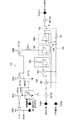
図4は、本実施形態に係るデータ転送回路200におけるPLL回路160、遅延調節部170、および遅延回路群180を含む遅延タイミング調整回路210の構成例を示す回路図である。 FIG. 4 is a circuit diagram showing a configuration example of the delay
PLL回路160は、マスタークロックMCKを分周した基準クロックRCLKに位相同期させたクロックを生成し、このクロックCLKをデジタル制御回路140に供給し、電流Idlを遅延調節部170に供給する。 The
PLL回路160は、図4に示すように、入力分周器(RDIV)161、位相比較器(PFD)162、チャージポンプ(CP)163、ループフィルタ(LPF)164、電圧制御発振器(VCO)165、および帰還分周器(1/N)166により構成される。 As shown in FIG. 4, the
PLL回路160は、入力分周器161にマスタークロックMCKが外部から供給され、チャージポンプ163に外部からバイアス信号BIASが供給され、帰還分周器166に外部から分周数制御信号DCTLが供給される。
入力分周器161は、マスタークロックMCKを入力分周器161で比較周波数まで分周し、基準クロックRCLKとして位相比較器162に出力する。
位相比較器162は、基準クロックRCLKと帰還分周器166からのフィードバッククロックFCLKとの位相差を検出し、その結果をチャージポンプ163に出力する。
チャージポンプ163およびループフィルタ164は、入力された位相差結果を時間軸から電圧軸に変換し、ループフィルタ164が電圧信号を電圧制御発振器165に出力する。
電圧制御発振器165は、ループフィルタ164で得られた電圧信号を入力として、発振器に流す電流を決め、電圧信号に応じた周波数で発振し、発振信号CLKを帰還分周器166に出力する。
帰還分周器166は、発振信号CLKの周波数をN分周し、分周した発信信号をフィードバッククロックFCLKとして位相比較器162に出力する。In the
The
The
The
The voltage controlled
The
図4の電圧制御発振器165は、pチャネルMOS(PMOS)トランジスタPT1〜PT7、nチャネルMOS(NMOS)トランジスタNT1,NT2,NT3、発振遅延素子OSCD1,OSCD2,OSCD3、および出力バッファBF1を有する。 4 includes p-channel MOS (PMOS) transistors PT1 to PT7, n-channel MOS (NMOS) transistors NT1, NT2, NT3, oscillation delay elements OSCD1, OSCD2, OSCD3, and an output buffer BF1.
PMOSトランジスタPT1およびPT2のソースが電源電圧VDDの供給源に接続されている。NMOSトランジスタNT1およびNT2のソースが基準電位源VSSに接続されている。
PMOSトランジスタPT1のドレインがNMOSトランジスタNT1のドレインに接続され、その接続点がPMOSトランジスタPT1のゲートおよびPMOSトランジスタPT2のゲートに接続されている。
NMOSトランジスタNT1のゲートがループフィルタ164の電圧信号の出力に接続されている。すなわち、NMOSトランジスタNT1のゲートにより電圧制御発振器165の入力部が形成される。
PMOSトランジスタPT2のドレインがNMOSトランジスタNT2のドレインおよびゲートに接続され、その接続点によりノードND1が形成されている。
これらのPMOSトランジスタPT1,PT2、およびNMOSトランジスタNT1,NT2によりカレントミラー回路が形成されている。The sources of the PMOS transistors PT1 and PT2 are connected to the supply source of the power supply voltage VDD. The sources of the NMOS transistors NT1 and NT2 are connected to the reference potential source VSS.
The drain of the PMOS transistor PT1 is connected to the drain of the NMOS transistor NT1, and the connection point is connected to the gate of the PMOS transistor PT1 and the gate of the PMOS transistor PT2.
The gate of the NMOS transistor NT1 is connected to the voltage signal output of the
The drain of the PMOS transistor PT2 is connected to the drain and gate of the NMOS transistor NT2, and a node ND1 is formed by the connection point.
These PMOS transistors PT1 and PT2 and NMOS transistors NT1 and NT2 form a current mirror circuit.
PMOSトランジスタPT3のソースが電源電圧VDDの供給源に接続され、ドレインがNMOSトランジスタNT3のドレインが接続され、その接続点により接続ノードND2が形成されている。NMOSトランジスタNT3のソースが基準電位源VSSに接続されている。
NMOSトランジスタNT3のゲートがノードND1に接続され、ノードND2がPMOSトランジスタPT3〜PT6のゲートに共通に接続されている。
これらのPMOSトランジスタPT3〜PT6、およびNMOSNT2,NT3によりカレントミラー回路が形成されている。
そして、ノードND2に電流Idlが発現される。
また、ノードND1に対してNMOSトランジスタNT3に並列にデータチャネル数分のNMOSトランジスタNT3−0〜NT3−pが配置される。そして、各NMOSトランジスタNT3−0〜NT3−pのドレインに発現される電流Idlが電流調節部170に供給される。
このNMOSトランジスタNT3−0〜NT3−pは、各チャネルに対応して配置される電流調節部170に配置されてもよい。The source of the PMOS transistor PT3 is connected to the supply source of the power supply voltage VDD, the drain is connected to the drain of the NMOS transistor NT3, and a connection node ND2 is formed by the connection point. The source of the NMOS transistor NT3 is connected to the reference potential source VSS.
The gate of the NMOS transistor NT3 is connected to the node ND1, and the node ND2 is commonly connected to the gates of the PMOS transistors PT3 to PT6.
These PMOS transistors PT3 to PT6 and NMOS NT2 and NT3 form a current mirror circuit.
Then, the current Idl is developed at the node ND2.
Further, NMOS transistors NT3-0 to NT3-p corresponding to the number of data channels are arranged in parallel with the NMOS transistor NT3 with respect to the node ND1. Then, the current Idl developed at the drains of the NMOS transistors NT3-0 to NT3-p is supplied to the
The NMOS transistors NT3-0 to NT3-p may be arranged in the
PMOSトランジスタPT4〜PT6のソースが電源電圧VDDの供給源に接続され、ドレインが発振遅延素子OSCD1、OSCD2,OSCD3の差動対に接続されている。
発振遅延素子OSCD1,OSCD2,OSCD3は、正負入力および負正出力を有する差動回路により構成される。そして、上記PMOSトランジスタPT3〜PT6は、各発振遅延素子OSCD1,OSCD2,OSCD3の電流源としてそれぞれ機能する。The sources of the PMOS transistors PT4 to PT6 are connected to the supply source of the power supply voltage VDD, and the drains are connected to the differential pair of the oscillation delay elements OSCD1, OSCD2, OSCD3.
The oscillation delay elements OSCD1, OSCD2, and OSCD3 are configured by differential circuits having positive and negative inputs and negative and positive outputs. The PMOS transistors PT3 to PT6 function as current sources for the oscillation delay elements OSCD1, OSCD2, and OSCD3, respectively.
3段の発振遅延素子OSCD1,OSCD2,OSCD3は、正負入力および負正出力が交互に縦続接続され、最終段の出力が初段の出力に帰還されて発振ループが形成されている。
具体的には、初段の発振遅延素子OSCD1の負出力が2段目のOSCD2の正入力に接続され、初段の発振遅延素子OSCD1の正出力が2段目のOSCD2の負入力に接続されている。
2段目の発振遅延素子OSCD2の負出力が最終段のOSCD3の正入力に接続され、2段目の発振遅延素子OSCD2の正出力が最終段のOSCD3の負入力に接続されている。
最終段の発振遅延素子OSCD3の負出力が初段のOSCD1の正入力に接続され、最終段の発振遅延素子OSCD3の正出力が初段のOSCD1の負入力に接続されている。
このように複数段(基本的に奇数段)の発振遅延素子OSCD1〜3をループ状に接続されて、電圧制御発振器165の発振部OSCが形成されている。The three stages of oscillation delay elements OSCD1, OSCD2, and OSCD3 have cascaded positive and negative inputs and negative and positive outputs, and the output of the final stage is fed back to the output of the first stage to form an oscillation loop.
Specifically, the negative output of the first stage oscillation delay element OSCD1 is connected to the positive input of the second stage OSCD2, and the positive output of the first stage oscillation delay element OSCD1 is connected to the negative input of the second stage OSCD2. .
The negative output of the second-stage oscillation delay element OSCD2 is connected to the positive input of the final-stage OSCD3, and the positive output of the second-stage oscillation delay element OSCD2 is connected to the negative input of the final-stage OSCD3.
The negative output of the final stage oscillation delay element OSCD3 is connected to the positive input of the first stage OSCD1, and the positive output of the final stage oscillation delay element OSCD3 is connected to the negative input of the first stage OSCD1.
In this way, the oscillation unit OSC of the voltage controlled
PMOSトランジスタPT7のソースが電源電圧VDDの供給源に接続され、ドレインが出力バッファBF1の差動対に接続されている。PMOSトランジスタPT7のゲートは制御信号CTLの供給ラインに接続されている。
出力バッファBF1は、正負入力および1正出力を有する差動回路により構成される。そして、上記PMOSトランジスタPT7は、出力バッファBF1の電流源として機能する。
出力バッファBF1の正入力が発振部OSCの最終段の発振遅延素子OSCD3の負出力に接続され、負入力が発振遅延素子OSCD3の正出力に接続されている。
出力バッファBF1は発振部OSCの差動出力をシングル信号に変換し、その発振信号CLKを帰還分周器166に出力する。The source of the PMOS transistor PT7 is connected to the supply source of the power supply voltage VDD, and the drain is connected to the differential pair of the output buffer BF1. The gate of the PMOS transistor PT7 is connected to the supply line of the control signal CTL.
The output buffer BF1 is composed of a differential circuit having positive and negative inputs and one positive output. The PMOS transistor PT7 functions as a current source for the output buffer BF1.
The positive input of the output buffer BF1 is connected to the negative output of the oscillation delay element OSCD3 in the final stage of the oscillation unit OSC, and the negative input is connected to the positive output of the oscillation delay element OSCD3.
The output buffer BF1 converts the differential output of the oscillation unit OSC into a single signal, and outputs the oscillation signal CLK to the
電流調節部170は、PLL回路160の電圧制御発振器165のノードND1の信号を受けて発振遅延素子OSCD1〜3の電流源としてのPMOSトランジスタPT4〜PT6に供給される電流Idlに応じた調節信号としての電流を発生する機能を有する。
電流調節部170は、供給電流Idlに応じた電流Ioscを発生し、電流Ioscを遅延回路181の遅延素子に調節信号として供給する。
電流調節部170は、外部からのデータまたはデータクロックの遅延制御信号DDCTL、DCCTLに応じて電流を微調整可能である。The
The
遅延回路群180は、データラインDTL0〜DTLpごとに配置された遅延回路181−0〜181−pを有する。
各遅延回路180−0〜181−pは、電流調節部170により供給される電流Ioscに応じた遅延量をもってデータの遅延量を調節し、このデータを出力インタフェース部150の対応するドライバ151−0〜151−pに出力する。The
Each delay circuit 180-0 ~181-p regulates a delay amount of data with a delay amount corresponding to the current Iosc supplied by the
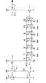
図5は、本実施形態に係る電流調節部170および遅延回路181の1チャネルあたりの構成例を示す図である。 FIG. 5 is a diagram illustrating a configuration example per channel of the
図5の電流調節部170は、PMOSトランジスタPT11〜PT14、ミラー比が調節可能な可変ゲート部171、およびNMOSトランジスタNT11を有する。 The
PMOSトランジスタPT11〜PT14のソースは電源電圧VDDの供給源に接続されている。NMOSトランジスタ11のソースは基準電位源VSSに接続されている。
PMOSトランジスタPT11のドレインが電流Idlの供給ラインに接続され、その接続ノードND11がPMOSトランジスタPT11のゲートおよびPMOSトランジスタPT12のゲートに接続されている。
PMOSトランジスタPT12のドレインが可変ゲート部171に接続され、その接続ノードND12がNMOSトランジスタNT11のゲートに接続されている。
PMOSトランジスタPT13のドレインがNMOSトランジスタNT11のドレインに接続され、その接続ノードND13がPMOSトランジスタPT13のゲートおよびPMOSトランジスタPT14のゲートに接続されている。
そして、PMOSトランジスタPT14のドレインから電流Ioscが遅延回路181の遅延素子に供給される。すなわち、PMOSトランジスタPT14は電流源として遅延回路181と共用される。The sources of the PMOS transistors PT11 to PT14 are connected to the supply source of the power supply voltage VDD. The source of the NMOS transistor 11 is connected to the reference potential source VSS.
The drain of the PMOS transistor PT11 is connected to the supply line of the current Idl, and the connection node ND11 is connected to the gate of the PMOS transistor PT11 and the gate of the PMOS transistor PT12.
The drain of the PMOS transistor PT12 is connected to the
The drain of the PMOS transistor PT13 is connected to the drain of the NMOS transistor NT11, and its connection node ND13 is connected to the gate of the PMOS transistor PT13 and the gate of the PMOS transistor PT14.
Then, the current Iosc is supplied from the drain of the PMOS transistor PT14 to the delay element of the
可変ゲート部171は、NMOSトランジスタNT12を基本としたカレントミラー回路を形成し、外部からの制御信号DDCTLまたはDCCTLによりそのミラー比を調節可能に構成される。 The
図6は、本実施形態に係る電流調節部170のより具体的な構成例を示す回路図である。
なお、図6においては、電流源I11、NMOSトランジスタNT13,NT14により形成されるカレントミラー回路で電流Idlを供給するように構成されている。FIG. 6 is a circuit diagram illustrating a more specific configuration example of the
In FIG. 6, the current Idl is supplied by a current mirror circuit formed by a current source I11 and NMOS transistors NT13 and NT14.
図6の可変ゲート部171は、ノードND12と基準電位源VSSとの間に並列に接続されたNMOSトランジスタNT12,NT121〜NT126を有する。
NMOSトランジスタNT12は、ゲートがノードND12に直接接続されている。
NMOSトランジスタNT121〜NT126は、各ゲートとノードND12とを選択的に接続するスイッチSW11と、各ゲートと基準電位源VSSとを選択的に接続するスイッチSW12とが接続されている。
スイッチSW11,SW12は、6ビットの制御信号DDCTLにより相補的にオンオフされる。
たとえば対応するビットが1の場合はスイッチSW11がオンし、スイッチSW12がオフする。一方、対応するビットが0の場合はスイッチSW11がオフし、スイッチSW12がオンする。
これにより、電流ミラー機能のミラー比Kが調節され、これに応じて電流Ioscが微調整される。The
The gate of the NMOS transistor NT12 is directly connected to the node ND12.
The NMOS transistors NT121 to NT126 are connected to a switch SW11 that selectively connects each gate and the node ND12 and a switch SW12 that selectively connects each gate and the reference potential source VSS.
The switches SW11 and SW12 are complementarily turned on and off by a 6-bit control signal DDCTL.
For example, when the corresponding bit is 1, the switch SW11 is turned on and the switch SW12 is turned off. On the other hand, when the corresponding bit is 0, the switch SW11 is turned off and the switch SW12 is turned on.
Thereby, the mirror ratio K of the current mirror function is adjusted, and the current Iosc is finely adjusted accordingly.
遅延回路群180の各遅延回路181(−0〜−p)は、図5に示すように、遅延素子182、入力レベルシフタ183、出力レベルシフタ184、クロックドインバータ185,186、インバータ187、およびスイッチ188,189を有する。
そして、スイッチ188,189、インバータ187によりバイパス回路190が形成されている。
遅延回路181は、バッファBF181,BF182、データ入力端子TDIN、スタンバイ信号STBの入力端子TSTB、および出力端子TDOUTを有する。
本実施形態において、スタンバイ信号STBはハイレベルでアクティブであり、非スタンバイ時にはローレベルに設定される。As shown in FIG. 5, each delay circuit 181 (−0 to −p) of the
A
In the present embodiment, the standby signal STB is active at a high level, and is set to a low level during non-standby.
バッファBF181の入力がデータ入力端子TDINに接続され、出力がクロックドインバータ185の入力およびスイッチ188の端子aに接続されている。スイッチ188の端子bは出力レベルシフタ184の出力およびスイッチ189の端子aに接続されている。
クロックドインバータ185の出力はクロックドインバータ186の入力および入力レベルシフタ183の負入力に接続されている。そして、クロックドインバータ186の出力が入力レベルシフタ183の正入力に接続されている。
クロックドインバータ185,186の制御端子はスタンバイ信号STBの入力端子TSTBに接続されている。
入力レベルシフタ183の正出力が遅延素子182の負入力に接続され、負出力が遅延素子182の正入力に接続されている。遅延素子182の正出力が出力レベルシフタ184の負入力に接続され、負出力が出力レベルシフタ184の正入力に接続されている。
出力レベルシフタ184の出力がスイッチ189の端子aに接続され、スイッチ189の端子bがバッファBF182の入力に接続され、バッファBF182の出力が出力端子TDOUTに接続されている。
また、スイッチ188の制御端子およびインバータ187の入力がスタンバイ信号STBの入力端子TSTBに接続され、インバータ187の出力がスイッチ189の制御端子に接続されている。Input buffer BF181 is connected to a data input terminal TDIN, the output is connected to the terminal a of the input and
The output of the clocked
Control terminals of the clocked
The positive output of the
The output of the
The control terminal of the
遅延素子182は、PLL回路160の電圧制御発振器165内の3段縦続接続された発振遅延素子OSCD1、OSCD2、OSCD3のうちの1段のたとえば発振遅延素子OSCD2と同一の(等価な)遅延素子により形成されている。
遅延素子182は、電流調節部170により電流Ioscを受けて、この電流Ioscの値に応じた遅延量をもって入力レベルシフタ183の出力データを遅延させ、そのデータを出力レベルシフタ184に出力する。
The
図7は、本実施形態に係る遅延回路181に適用される遅延素子182の構成例を示す回路図である。 FIG. 7 is a circuit diagram showing a configuration example of the
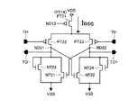
図7の遅延素子182は、PMOSトランジスタPT21,PT22,PT23、NMOSトランジスタNT21〜NT24、入力端子TI+,TI−、および出力端子TO+,TO−を有する。
なお、遅延素子182において、電流源としてのPMOSトランジスタPT21は図5に示す電流調節部170と共用するPMOSトランジスタPT14に相当する。The
In the
PMOSトランジスタPT21のソースが電源電圧VDDの供給源に接続され、ドレインがPMOSトランジスタPT22,PT23のソースに接続されている。
PMOSトランジスタPT21のゲートは、図5に示したように、ノードND13に接続されている。
PMOSトランジスタPT22のドレインがNMOSトランジスタNT21、NT23のドレインに接続され、その接続点によりノードND21が形成されている。PMOSトランジスタPT22のゲートが正の入力端子TI+に接続され、ノードND21が負の出力端子TO−に接続されている。正の入力端子TI+は上述したように、入力レベルシフタ183の負出力に接続され、負の出力端子TO−は出力レベルシフタ184の正入力に接続される。
PMOSトランジスタPT23のドレインがNMOSトランジスタNT22、NT24のドレインに接続され、その接続点によりノードND23が形成されている。PMOSトランジスタPT23のゲートが負の入力端子TI−に接続され、ノードND22が正の出力端子TO+に接続されている。負の入力端子TI−は上述したように、入力レベルシフタ183の正出力に接続され、正の出力端子TO+は出力レベルシフタ184の負入力に接続される。
NMOSトランジスタNT21およびNT23のソースが基準電位源VSSに接続されている。NMOSトランジスタNT21のゲートがノードND22に接続され、NMOSトランジスタNT23ゲートは自身のドレインおよびノードND21に接続されている。NMOSトランジスタNT23はダイオード接続されており、ノードND21の電位を所定電位に保持するリミッタとして機能する。
NMOSトランジスタNT22およびNT24のソースが基準電位源VSSに接続されている。NMOSトランジスタNT22のゲートがノードND21に接続され、NMOSトランジスタNT24ゲートは自身のドレインおよびノードND22に接続されている。NMOSトランジスタNT24はダイオード接続されており、ノードND22の電位を所定電位に保持するリミッタとして機能する。The source of the PMOS transistor PT21 is connected to the supply source of the power supply voltage VDD, and the drain is connected to the sources of the PMOS transistors PT22 and PT23.
The gate of the PMOS transistor PT21 is connected to the node ND13 as shown in FIG.
The drain of the PMOS transistor PT22 is connected to the drains of the NMOS transistors NT21 and NT23, and a node ND21 is formed by the connection point. The gate of the PMOS transistor PT22 is connected to the positive input terminal TI +, and the node ND21 is connected to the negative output terminal TO−. As described above, the positive input terminal TI + is connected to the negative output of the
The drain of the PMOS transistor PT23 is connected to the drains of the NMOS transistors NT22 and NT24, and a node ND23 is formed by the connection point. The gate of the PMOS transistor PT23 is connected to the negative input terminal TI−, and the node ND22 is connected to the positive output terminal TO +. The negative input terminal TI-, as described above, is connected to the positive output of the
The sources of the NMOS transistors NT21 and NT23 are connected to the reference potential source VSS. The gate of the NMOS transistor NT21 is connected to the node ND22, and the gate of the NMOS transistor NT23 is connected to its own drain and the node ND21. The NMOS transistor NT23 is diode-connected and functions as a limiter that holds the potential of the node ND21 at a predetermined potential.
The sources of the NMOS transistors NT22 and NT24 are connected to the reference potential source VSS. The gate of the NMOS transistor NT22 is connected to the node ND21, and the gate of the NMOS transistor NT24 is connected to its own drain and the node ND22. The NMOS transistor NT24 is diode-connected and functions as a limiter that holds the potential of the node ND22 at a predetermined potential.
このような構成を有する遅延素子182は、正の入力端子TI+に入力するデータのレベルを反転させて負の出力端子TO−から出力し、負の入力端子TI−に入力するデータのレベルを反転させて正の出力端子TO+から出力する。
このレベル反転動作の処理時間が電流調節部170から供給される電流Ioscの値で調節される。The
The processing time of the level inversion operation is adjusted by the value of the current Iosc supplied from the
入力レベルシフタ183は、クロックドインバータ185,186から出力される入力データの電圧振幅を次段の遅延素子182(osc)の入力電圧レンジに調節し、振幅調整したデータを遅延素子182に出力する。
たとえば遅延素子182の入力電圧レンジは、電圧最大値VMAXと電圧最小値VMINの範囲である。The
For example, the input voltage range of the
図8は、本実施形態に係る遅延回路181に適用される入力レベルシフタ183の構成例を示す回路図である。 FIG. 8 is a circuit diagram showing a configuration example of the
入力差動回路1831、および出力バッファ部1832,1833を有する。 An
入力差動回路1831は、PMOSトランジスタPT31、PT32、NMOSトランジスタNT31,NT32、正の入力端子TI+、および負の入力端子TI−を有する。
PMOSトランジスタPT31およびPT32のソースが電源電圧VDDの供給源に接続され、NMOSトランジスタNT31およびNT32のソースが基準電位源VSSに接続されている。
PMOSトランジスタPT31のゲートが正の入力端子TI+に接続され、ドレインがNMOSトランジスタNT31のドレインに接続され、その接続点によりノードND31が形成されている。
PMOSトランジスタPT32のゲートが負の入力端子TI−に接続され、ドレインがNMOSトランジスタNT32のドレインに接続され、その接続点によりノードND32が形成されている。
NMOSトランジスタNT31のゲートがノードND32に接続され、NMOSトランジスタNT32のゲートがノードND31に接続されている。
そして、ノードND31が出力バッファ部1832の入力に接続され、ノードND32が出力バッファ部1833の入力に接続されている。The
The sources of the PMOS transistors PT31 and PT32 are connected to the supply source of the power supply voltage VDD, and the sources of the NMOS transistors NT31 and NT32 are connected to the reference potential source VSS.
The gate of the PMOS transistor PT31 is connected to the positive input terminal TI +, the drain is connected to the drain of the NMOS transistor NT31, and a node ND31 is formed by the connection point.
The gate of the PMOS transistor PT32 is connected to the negative input terminal TI−, the drain is connected to the drain of the NMOS transistor NT32, and a node ND32 is formed by the connection point.
The gate of the NMOS transistor NT31 is connected to the node ND32, and the gate of the NMOS transistor NT32 is connected to the node ND31.
The node ND31 is connected to the input of the
出力バッファ部1832は、PMOSトランジスタPT33,PT34、NMOSトランジスタNT33,NT34,および負の出力端子TO−を有する。
PMOSトランジスタPT33,PT34のソースが遅延素子182の電圧最大値VMAXの供給端子TVMAXに接続されている。
NMOSトランジスタNT33,NT34のソースが遅延素子182の電圧最小値VMINの供給端子TVMINに接続されている。
PMOSトランジスタPT33のドレインがNMOSトランジスタNT33のドレインと接続され、その接続点によりノードND33が形成されている。
PMOSトランジスタPT34のドレインがNMOSトランジスタNT34のドレインと接続され、その接続点によりノードND34が形成されている。
PMOSトランジスタPT33のゲートおよびNMOSトランジスタNT33のゲートが入力差動回路1831のノードND31に接続されている。
PMOSトランジスタPT34のゲートおよびNMOSトランジスタNT34のゲートがノードND33に接続され、ノードND34が負の出力端子TO−に接続されている。
すなわち、出力バッファ部1832は、ノードND31と出力端子TO−との間に2つのCMOSインバータを縦続接続して構成されている。The
The sources of the PMOS transistors PT33 and PT34 are connected to the supply terminal TVMAX for the voltage maximum value VMAX of the
The sources of the NMOS transistors NT33 and NT34 are connected to the supply terminal TVMIN of the voltage minimum value VMIN of the
The drain of the PMOS transistor PT33 is connected to the drain of the NMOS transistor NT33, and a node ND33 is formed by the connection point.
The drain of the PMOS transistor PT34 is connected to the drain of the NMOS transistor NT34, and a node ND34 is formed by the connection point.
The gate of the PMOS transistor PT33 and the gate of the NMOS transistor NT33 are connected to the node ND31 of the
The gate of the PMOS transistor PT34 and the gate of the NMOS transistor NT34 are connected to the node ND33, and the node ND34 is connected to the negative output terminal TO−.
That is, the
出力バッファ部1833は、PMOSトランジスタPT33,PT34、NMOSトランジスタNT33,NT34,および正の出力端子TO+を有する。
PMOSトランジスタPT35,PT36のソースが遅延素子182の電圧最大値VMAXの供給端子TVMAXに接続されている。
NMOSトランジスタNT35,NT36のソースが遅延素子182の電圧最小値VMINの供給端子TVMINに接続されている。
PMOSトランジスタPT35のドレインがNMOSトランジスタNT35のドレインと接続され、その接続点によりノードND35が形成されている。
PMOSトランジスタPT36のドレインがNMOSトランジスタNT36のドレインと接続され、その接続点によりノードND36が形成されている。
PMOSトランジスタPT35のゲートおよびNMOSトランジスタNT35のゲートが入力差動回路1831のノードND32に接続されている。
PMOSトランジスタPT36のゲートおよびNMOSトランジスタNT36のゲートがノードND35に接続され、ノードND36が正の出力端子TO+に接続されている。
すなわち、出力バッファ部1833は、ノードND32と出力端子TO+との間に2つのCMOSインバータを縦続接続して構成されている。The
The sources of the PMOS transistors PT35 and PT36 are connected to the supply terminal TVMAX of the voltage maximum value VMAX of the
The sources of the NMOS transistors NT35 and NT36 are connected to the supply terminal TVMIN of the voltage minimum value VMIN of the
The drain of the PMOS transistor PT35 is connected to the drain of the NMOS transistor NT35, and a node ND35 is formed by the connection point.
The drain of the PMOS transistor PT36 is connected to the drain of the NMOS transistor NT36, and a node ND36 is formed by the connection point.
The gate of the PMOS transistor PT35 and the gate of the NMOS transistor NT35 are connected to the node ND32 of the
The gate of the PMOS transistor PT36 and the gate of the NMOS transistor NT36 are connected to the node ND35, and the node ND36 is connected to the positive output terminal TO +.
That is, the
入力レベルシフタ183は、正の入力端子TI+に入力するデータを入力差動回路1831でレベルを反転させ、出力バッファ部1832でデータの電圧振幅を次段の遅延素子182の入力電圧レンジに調節し、負の出力端子TO−から出力する。
また、入力レベルシフタ183は、負の入力端子TI−に入力するデータを入力差動回路1831でレベルを反転させ、出力バッファ部1833でデータの電圧振幅を次段の遅延素子182の入力電圧レンジに調節し、正の出力端子TO+から出力する。The
The
出力レベルシフタ184は、遅延素子182から出力されたデータの出力電圧振幅を再びデータの電圧振幅(VDD−VSS)に戻し、差動からシングルに出力を変換する。 The
図9は、本実施形態に係る遅延回路181に適用される出力レベルシフタ184の構成例を示す回路図である。 FIG. 9 is a circuit diagram showing a configuration example of the
図9の出力レベルシフタ184は、PMOSトランジスタPT41、PT42、NMOSトランジスタNT41,NT42、正の入力端子TI+、負の入力端子TI−、および出力端子TOを有する。
PMOSトランジスタPT41およびPT42のソースが電源電圧VDDの供給源に接続され、NMOSトランジスタNT41およびNT42のソースが基準電位源VSSに接続されている。
PMOSトランジスタPT41のゲートが正の入力端子TI+に接続され、ドレインがNMOSトランジスタNT41のドレインに接続され、その接続点によりノードND41が形成されている。
PMOSトランジスタPT42のゲートが負の入力端子TI−に接続され、ドレインがNMOSトランジスタNT42のドレインに接続され、その接続点によりノードND42が形成されている。
NMOSトランジスタNT41,NT42のゲートがノードND41に接続され、ノードND42が出力端子TOに接続されている。The
The sources of the PMOS transistors PT41 and PT42 are connected to the supply source of the power supply voltage VDD, and the sources of the NMOS transistors NT41 and NT42 are connected to the reference potential source VSS.
The gate of the PMOS transistor PT41 is connected to the positive input terminal TI +, the drain is connected to the drain of the NMOS transistor NT41, and a node ND41 is formed by the connection point.
The gate of the PMOS transistor PT42 is connected to thenegative input terminal TI−, the drain is connected to the drain of the NMOS transistor NT42, and a node ND42 is formed by the connection point.
The gates of the NMOS transistors NT41 and NT42 are connected to the node ND41, and the node ND42 is connected to the output terminal TO.
このような構成を有する出力レベルシフタ184は、上述したように、遅延素子182から出力されたデータの出力電圧振幅を再びデータの電圧振幅(VDD−VSS)に戻し、差動からシングルに出力を変換する。 As described above, the
クロックドインバータ185,186はスタンバイ信号STBが非アクティブのローレベルのときに作動状態となり、入力データを反転して出力する。
スイッチ188,189はスタンバイ信号STBがハイレベルのときにオン状態となり、入力データの経路において、バッファBF181の出力を出力レベルシフタ184側に直接転送する。
すなわち、スイッチ188は、スタンバイ信号STBがアクティブのハイレベルのときに、データ経路におけるクロックドインバータ185,186、入力レベルシフタ183、遅延素子182、出力レベルシフタ184の経路をバイパスさせる。
スイッチ189は、スタンバイ信号STBがローレベルでインバータ187の出力がハイレベルのときにオン状態となり、出力レベルシフタ184の出力をバッファBF182を介して出力端子TDOUTに伝搬させる。
スイッチ189は、スタンバイ信号STBがハイレベルでインバータ187の出力がローレベルのときにオフ状態となり、出力レベルシフタ184の出力側をハイインピーダンス状態に保持する。The clocked
The
That is, the
The
The
ここで、上記構成を有するデータ転送回路200における遅延タイミング調整回路210の動作について、図10、図11(A)〜(D)、および図12(A)〜(D)に関連付けて説明する。
図10は、遅延時間Tdと供給電流Ioscとの関係を説明するための図である。
図11(A)〜(D)は通常動作(非スタンバイ)時のタイミングチャートである。
図12(A)〜(D)はスタンバイ時のタイミングチャートである。Here, the operation of the delay
FIG. 10 is a diagram for explaining the relationship between the delay time Td and the supply current Iosc.
11A to 11D are timing charts during normal operation (non-standby).
12A to 12D are timing charts during standby.
PLL回路160は、マスタークロックMCKを入力分周器161で比較周波数まで分周をかけた後、この基準クロックRCLKと帰還分周器166からのフィードバッククロックFCLKと位相比較器162で位相差を検出する。
検出された位相差はチャージポンプ163とループフィルタ164にて時間軸から電圧軸に変換される。
電圧制御発振器165の出力は帰還分周器166に供給され、そこで比較周波数に分周され位相比較器162にフィードバックされる。そして、フィードバッククロックFCLKと分周後のマスタークロックである基準クロックRCLKの位相が一致する周波数でロックがかかる。The
The detected phase difference is converted from the time axis to the voltage axis by the
The output of the voltage controlled
このフィードバック制御により、温度変化や電源電圧変動、トランジスタのしきい値バラツキ等が発生した際にもロック周波数は一定となり、発振器で生じる位相差はこれらの変動の影響を受けずに安定する。
本実施形態においては、この位相差が遅延回路181の遅延時間の基準値として使用される。
ロック周波数はマスタークロックMCKの周波数、帰還分周器166の分周数、電圧制御発振器165のゲイン、チャージポンプ163の出力電流、ループフィルタ164の伝達関数により決定される。
ただし、本遅延タイミング調整回路210ではPLL回路160のロック周波数は直接遅延時間として使用しないため、任意のロック周波数に設定することが可能である。This feedback control makes the lock frequency constant even when temperature changes, power supply voltage fluctuations, transistor threshold variations, and the like occur, and the phase difference generated by the oscillator is stabilized without being affected by these fluctuations.
In the present embodiment, this phase difference is used as a reference value for the delay time of the
The lock frequency is determined by the frequency of the master clock MCK, the frequency division number of the
However, in the present delay
遅延回路181はPLL回路160の電圧制御発振器165から発振遅延素子OSCD1〜3の供給電流Idlを受け取る。
この電流IdlはPLL回路160の電圧制御発振器165の発振遅延素子OSCD1〜3に供給されるものをミラー(折り返し)したものである。このため、遅延回路181の遅延素子182で生じる位相差はPLL回路160の発振遅延素子OSCD1〜3のうちの1段で生じる位相差と同一のものとなる。
したがって、遅延回路181の遅延素子182cで生じる位相差もPLL回路160と同様に温度変化、電源電圧変動、トランジスタのしきい値バラツキの影響を受けない。
This current Idl is a mirror (turned back) of the current supplied to the oscillation delay elements OSCD1 to OSCD1-3 of the voltage controlled
Therefore, the phase difference generated in the delay element 182c of the
遅延タイミング調整回路210は、図5および図6に示すように、電流調節部(遅延調節部)170にてPLL回路160から供給される電流Idlを微調整することが可能である。
この図5および図6例の場合、遅延時間Tdと遅延素子182への供給電流Ioscは以下のような関係式が成り立つ。As shown in FIGS. 5 and 6, the delay
In the example of FIGS. 5 and 6, the following relational expression is established between the delay time Td and the supply current Iosc to the
[数1]
ΔTd ∝ 1/√ΔIosc ・・・(式1)[Equation 1]
ΔTd ∝ 1 / √ΔIosc (Formula 1)
このことから以下のように電流調節部(遅延調節部)170で電流Ioscを制御することで、遅延時間Tdを線形に調節することが可能である。 Thus, the delay time Td can be linearly adjusted by controlling the current Iosc by the current adjustment unit (delay adjustment unit) 170 as described below.
[数2]
ΔIosc = Idl/ΔK ・・・(式2)[Equation 2]
ΔIosc = Idl / ΔK (Formula 2)
ここで、Kは電流調節部(遅延調節部)170の電流調節係数を示す。IdlはPLL回路160から電流調節部(遅延調節部)170に供給される電流を現している。
ここで、式2を式1に代入すると、次の関係が得られる。Here, K indicates a current adjustment coefficient of the current adjustment unit (delay adjustment unit) 170. Idl represents the current supplied from the
Here, substituting
[数3]
ΔTd ∝ √ΔK/√Idl ・・・(式3)[Equation 3]
ΔTd ∝ √ΔK / √Idl (Formula 3)
√Idlは定数であることから、式3を変形すると次式が得られる。 Since Idl is a constant, the following equation can be obtained by transforming Equation 3.
[数4]
∴ΔTd ∝ √ΔK ・・・(式4)[Equation 4]
∴ΔTd ∝ √ΔK (Formula 4)
遅延時間Tdと電流調節部(遅延調節部)170による電流調節係数Kの平方根とが比例関係になる。
図10は、供給電流Ioscと遅延時間Tdとの関係をグラフ化したものである。
電流調節部(遅延調節部)170は、図5および図6に示されるように、カレントミラー構成であり、ミラー比を外部からの制御信号DDCTLで調節できるように設定可能な構成となっている。
このミラー比がKに相当する。
電流調節部(遅延調節部)170は、カレントミラー比を制御信号DDCTLで切り替えられる構成であるため、ミラー比Kの選び方次第で平方根特性も実現可能である。
たとえば、Kを1,4,9,16,25・・・と切り替えた場合、Kの平方根は1,2,3,4,5・・・となり、ΔTdは線形に増加していくことが確認できる。The delay time Td and the square root of the current adjustment coefficient K by the current adjustment unit (delay adjustment unit) 170 have a proportional relationship.
FIG. 10 is a graph showing the relationship between the supply current Iosc and the delay time Td.
As shown in FIGS. 5 and 6, the current adjustment unit (delay adjustment unit) 170 has a current mirror configuration and can be set so that the mirror ratio can be adjusted by an external control signal DDCTL. .
This mirror ratio corresponds to K.
Since the current adjustment unit (delay adjustment unit) 170 has a configuration in which the current mirror ratio can be switched by the control signal DDCTL, a square root characteristic can be realized depending on how the mirror ratio K is selected.
For example, when K is switched to 1, 4, 9, 16, 25..., The square root of K becomes 1, 2, 3, 4, 5,... And ΔTd increases linearly. it can.
図6に電流調節部(遅延調節部)170の回路例を示すように、電流調節部(遅延調節部)170は6ビット制御の回路となっているが、6ビットに限定されることなく、目標とするΔTdにあわせてビット数を調節することが可能である。 As shown in the circuit example of the current adjustment unit (delay adjustment unit) 170 in FIG. 6, the current adjustment unit (delay adjustment unit) 170 is a 6-bit control circuit, but is not limited to 6 bits. It is possible to adjust the number of bits according to the target ΔTd.
以上のように、通常動作時(非スタンバイ時)には、遅延回路181でタイミング調整され、出力インタフェース部150を介して伝送線路400に出力される。 As described above, during normal operation (non-standby), the timing is adjusted by the
遅延回路181を使わない場合、スタンバイ信号STBがハイレベルに設定されて入力されることで、遅延回路181の入力レベルシフタ183、遅延素子182、出力レベルシフタ184をバイパスする経路で信号を送ることになる。
この場合、バッファの遅延のみに切り替えることができる。
このとき、入力レベルシフタ183、遅延素子182、出力レベルシフタ184は連動してスタンバイ状態となり、消費電力を抑えることができる。
なお、このときの出力レベルシフタ184の出力端子はハイインピーダンスに設定する。
たとえば、イメージセンサのデータレートを落とした際に、出力チャネルの数がそれに連動して減るとすると、減らされた出力チャネルはスタンバイに落とすことで、消費電力の削減を可能としている。When the
In this case, only the buffer delay can be switched.
At this time, the
At this time, the output terminal of the
For example, when the data rate of the image sensor is reduced, if the number of output channels decreases in conjunction with it, the reduced output channels are reduced to standby, thereby reducing power consumption.
上述したように、図11(A)〜(D)が遅延回路動作時を、図12(A)〜(D)が遅延回路をバイパスした場合の入出力関係を表している。
スタンバイ信号STBがローレベルの場合、入力レベルシフタ183、遅延素子182、出力レベルシフタ184を介する。これにより、入力データDATAINに対して、制御信号DDCTLのミラーKの値に比例した遅延時間Tdだけ遅れて出力データDATAOUTが出力される。
スタンバイ信号STBがハイレベルになると、入力レベルシフタ183、遅延素子182、出力レベルシフタ184はスタンバイ状態となり、遅延時間Tdはほぼ0となる。As described above, FIGS. 11A to 11D show the input / output relationship when the delay circuit is operating, and FIGS. 12A to 12D show the input / output relationship when the delay circuit is bypassed.
When the standby signal STB is at the low level, the input signal is shifted through the
When the standby signal STB becomes high level, the
以上説明したように、本実施形態によれば、遅延タイミング調整回路210はPLL回路160を内蔵する。そして、PLL回路160の発振遅延素子と同一のものを遅延回路181の遅延素子182として使用することで温度変化、電源電圧変動、トランジスタのしきい値バラツキに依存しない遅延時間を作り出すことが可能である。
また、遅延タイミング調整回路210は、遅延回路181の遅延素子182に供給する電流を調節する電流調節部170を有しており、多チャネルインタフェースに応用する場合に各遅延回路毎に独立して遅延時間を設定することが可能である。
遅延タイミング調整回路210は、各データラインDTL0〜DTLp上に配置する回路がDLLに比べて少ないため、DLLに比べて小型化が可能であり、イメージセンサ等の周辺回路の小型化が必要なものに適している。
遅延タイミング調整回路210は、PLL回路160内部の発振遅延素子OSCD1〜3で生じる位相差を直接遅延時間として使用するのではない。このため、遅延時間に依らずPLL回路160のロック周波数を任意に定めることが可能であり、PLL回路160の設計難易度を下げることが可能である。As described above, according to the present embodiment, the delay
The delay
The delay
The delay
なお、各実施形態に係るCMOSイメージセンサは、特に限定されないが、たとえば列並列型のアナログ−デジタル変換装置(カラムADC(Analog digital converter)を搭載したCMOSイメージセンサとして構成することも可能である。 The CMOS image sensor according to each embodiment is not particularly limited, but may be configured as, for example, a CMOS image sensor equipped with a column parallel type analog-digital converter (column ADC (Analog digital converter)).
このような効果を有する固体撮像素子は、デジタルカメラやビデオカメラの撮像デバイスとして適用することができる。 A solid-state imaging device having such an effect can be applied as an imaging device for a digital camera or a video camera.
<2.第2の実施形態>
図13は、本発明の実施形態に係る固体撮像素子が適用されるカメラシステムの構成の一例を示す図である。<2. Second Embodiment>
FIG. 13 is a diagram illustrating an example of a configuration of a camera system to which the solid-state imaging device according to the embodiment of the present invention is applied.
本カメラシステム500は、図13に示すように、本実施形態に係るCMOSイメージセンサ(固体撮像素子)100が適用可能な撮像デバイス510を有する。
カメラシステム500は、この撮像デバイス510の画素領域に入射光を導く(被写体像を結像する)光学系、たとえば入射光(像光)を撮像面上に結像させるレンズ520を有する。
また、カメラシステム500は、撮像デバイス510を駆動する駆動回路(DRV)530と、撮像デバイス510の出力信号を処理する信号処理回路(PRC)540と、を有する。As shown in FIG. 13, the
The
In addition, the
駆動回路530は、撮像デバイス510内の回路を駆動するスタートパルスやクロックパルスを含む各種のタイミング信号を生成するタイミングジェネレータ(図示せず)を有し、所定のタイミング信号で撮像デバイス510を駆動する。 The
また、信号処理回路540は、撮像デバイス510の出力信号に対して所定の信号処理を施す。
信号処理回路540で処理された画像信号は、たとえばメモリなどの記録媒体に記録される。記録媒体に記録された画像情報は、プリンタなどによってハードコピーされる。また、信号処理回路540で処理された画像信号を液晶ディスプレイ等からなるモニターに動画として映し出される。The
The image signal processed by the
上述したように、デジタルスチルカメラ等の撮像装置において、撮像デバイス510として、先述した撮像素子100を搭載することで、低消費電力で、高精度なカメラが実現できる。 As described above, by mounting the above-described
100・・・CMOSイメージセンサ(固体撮像素子)、110・・・画素アレイ部、120・・・行選択回路(Vdec)、130・・・カラム読み出し回路(AFE)、140・・・デジタル制御回路、150・・・出力インタフェース部(IF)、160・・・PLL回路、161・・・入力分周器(RDIV)、162・・・位相比較器(PFD)、163・・・チャージポンプ(CP)、164・・・ループフィルタ(LPF)、165・・・電圧制御発振器(VCO)、OSCD1〜3・・・発振遅延素子、166・・・帰還分周器(1/N)、170・・・遅延調節部(電流調節部)、180・・・遅延回路群、181・・・遅延回路、182・・・遅延素子、183・・・入力レベルシフタ、184・・・出力レベルシフタ、200・・・データ転送回路、210・・・遅延タイミング調整回路、500・・・カメラシステム、510・・・撮像デバイス、520・・・レンズ、530・・・駆動回路、540・・・信号処理回路。 DESCRIPTION OF
Claims (13)
Translated fromJapanese発振信号を発振する複数の発振遅延素子を有し、基準クロックとフィードバッククロックとを位相同期させて上記発振信号を発振する位相同期回路と、
上記データラインに配置された上記発振遅延素子と等価な遅延素子を含み、当該データラインを伝搬されるデータを遅延させる、上記複数のデータラインにそれぞれ配置された複数の遅延回路と、
上記遅延回路ごとに独立して配置され、上記位相同期回路の発振にかかわる信号に応じて対応する上記遅延回路の遅延素子の遅延量を調節する複数の遅延調節部と、を有し、
上記位相同期回路は、
基準クロックとフィードバッククロックとの位相比較結果に応じた電圧を受けて、カレントミラー回路により得られた電流を上記発振遅延素子の電流源に供給して発振動作を行う電圧制御発振器を含み、
上記遅延調節部は、
上記位相同期回路のカレントミラー回路により得られた上記電流に応じた電流を、少なくとも一つのカレントミラー回路を介して対応する上記遅延回路の上記遅延素子の遅延量を調節する調節信号として当該遅延素子の電流源に供給する
タイミング調整回路。Multiple data lines,
A plurality of oscillation delay elements that oscillate an oscillation signal, a phase synchronization circuit that oscillates the oscillation signal by synchronizing the phase of a reference clock and a feedback clock, and
A plurality of delay circuits each disposed in the plurality of data lines, each including a delay element equivalent to the oscillation delay element disposed in the data line, and delaying data propagated through the data line;
A plurality of delay adjusting units that are arranged independently for each of the delay circuits and adjust the delay amount of the delay element of the delay circuit corresponding to a signal related to the oscillation of the phase synchronization circuit;
The phase synchronization circuit is
A voltage controlled oscillator that receives a voltage according to a phase comparison result between a reference clock and a feedback clock, and supplies a current obtained by a current mirror circuit to a current source of the oscillation delay element to perform an oscillation operation;
The delay adjuster is
The current corresponding to the current obtained by the current mirror circuit of the phase-locked loop circuit is used as an adjustment signal for adjusting the delay amount of the delay element of the corresponding delay circuit via at least one current mirror circuit. Timing adjustment circuit to supply current source.
上記位相同期回路のカレントミラー回路により得られた上記電流を折り返す第1のカレントミラー回路と、
ミラー比を調整可能で、上記第1のカレントミラー回路による電流を折り返す第2のカレントミラー回路と、を含み、
上記第2のカレントミラー回路による電流を上記遅延素子の電流源に当該遅延素子の遅延量を調節する調節信号として供給する
請求項1記載のタイミング調整回路。The delayadjuster is
A first current mirror circuit that turns back the current obtained by the current mirror circuit of the phase synchronization circuit;
A mirror ratio is adjustable, and a second current mirror circuit that folds back the current by the first current mirror circuit,
The timing adjustment circuit according to claim 1, wherein the current from the second current mirror circuit is supplied to the current source of the delay element as an adjustment signal for adjusting a delay amount of the delay element.
制御信号に応じて上記遅延素子に供給する電流を微調整可能な機能を有する
請求項1または2記載のタイミング調整回路。The delay adjuster is
The timing adjustment circuit according to claim 1, wherein the timing adjustment circuit has a function of finely adjusting a current supplied to the delay element in accordance with a control signal.
少なくとも上記遅延素子の入力側に配置され、入力データを上記遅延素子の入力電圧レンジに調節し、レベル調節したデータを当該遅延素子に供給する入力レベルシフタと、
上記遅延素子から出力されたデータの出力振幅電圧をデータの電圧振幅に戻す出力レベルシフタと、
スタンバイ時に、上記入力レベルシフタ、上記遅延素子、および上記出力レベルシフタのデータ経路をバイパスして、入力データを上記出力レベルシフタの出力側にバイパスするバイパス回路と、を含む
請求項1から3のいずれか一に記載のタイミング調整回路。The delay circuit is
An input level shifter that is arranged at least on the input side of the delay element, adjusts the input data to the input voltage range of the delay element, and supplies the level-adjusted data to the delay element;
An output level shifter for returning the output amplitude voltage of the data output from the delay element to the voltage amplitude of the data;
4. A bypass circuit that bypasses the data path of the input level shifter, the delay element, and the output level shifter during standby and bypasses input data to the output side of the output level shifter. 5. The timing adjustment circuit described in 1.
上記スタンバイ時に、上記出力レベルシフタの出力側をハイインピーダンスに保持する機能を有する
請求項4記載のタイミング調整回路。The bypass circuit is
The timing adjustment circuit according to claim 4, wherein the timing adjustment circuit has a function of holding the output side of the output level shifter at a high impedance during the standby.
上記画素部から画素信号の読み出しを行い、読み出したアナログ画素信号をデジタル信号に変換する機能を含む画素読み出し部と、
上記画素読み出し部によるデジタル信号の遅延タイミングを調整可能なタイミング調整回路と、を有し、
上記タイミング調整回路は、
複数のデータラインと、
発振信号を発振する複数の発振遅延素子を有し、基準クロックとフィードバッククロックとを位相同期させて上記発振信号を発振する位相同期回路と、
上記データラインに配置された上記発振遅延素子と等価な遅延素子を含み、当該データラインを伝搬されるデータを遅延させる、上記複数のデータラインにそれぞれ配置された複数の遅延回路と、
上記遅延回路ごとに独立して配置され、上記位相同期回路の発振にかかわる信号に応じて対応する上記遅延回路の遅延素子の遅延量を調節する複数の遅延調節部と、を有し、
上記位相同期回路は、
基準クロックとフィードバッククロックとの位相比較結果に応じた電圧を受けて、カレントミラー回路により得られた電流を上記発振遅延素子の電流源に供給して発振動作を行う電圧制御発振器を含み、
上記遅延調節部は、
上記位相同期回路のカレントミラー回路により得られた上記電流に応じた電流を、少なくとも一つのカレントミラー回路を介して対応する上記遅延回路の上記遅延素子の遅延量を調節する調節信号として当該遅延素子の電流源に供給する
固体撮像素子。A pixel unit in which a plurality of pixels that perform photoelectric conversion are arranged in a matrix;
A pixel readout unit including a function of reading out a pixel signal from the pixel unit and converting the readout analog pixel signal into a digital signal;
A timing adjustment circuit capable of adjusting the delay timing of the digital signal by the pixel readout unit,
The timing adjustment circuit is
Multiple data lines,
A plurality of oscillation delay elements that oscillate an oscillation signal, a phase synchronization circuit that oscillates the oscillation signal by synchronizing the phase of a reference clock and a feedback clock, and
A plurality of delay circuits each disposed in the plurality of data lines, each including a delay element equivalent to the oscillation delay element disposed in the data line, and delaying data propagated through the data line;
A plurality of delay adjusting units that are arranged independently for each of the delay circuits and adjust the delay amount of the delay element of the delay circuit corresponding to a signal related to the oscillation of the phase synchronization circuit;
The phase synchronization circuit is
A voltage controlled oscillator that receives a voltage according to a phase comparison result between a reference clock and a feedback clock, and supplies a current obtained by a current mirror circuit to a current source of the oscillation delay element to perform an oscillation operation;
The delay adjuster is
The current corresponding to the current obtained by the current mirror circuit of the phase-locked loop circuit is used as an adjustment signal for adjusting the delay amount of the delay element of the corresponding delay circuit via at least one current mirror circuit. A solid-state image sensor that supplies a current source.
上記位相同期回路のカレントミラー回路により得られた上記電流を折り返す第1のカレントミラー回路と、
ミラー比を調整可能で、上記第1のカレントミラー回路による電流を折り返す第2のカレントミラー回路と、を含み、
上記第2のカレントミラー回路による電流を上記遅延素子の電流源に当該遅延素子の遅延量を調節する調節信号として供給する
請求項6記載の固体撮像素子。The delayadjuster is
A first current mirror circuit that turns back the current obtained by the current mirror circuit of the phase synchronization circuit;
A mirror ratio is adjustable, and a second current mirror circuit that folds back the current by the first current mirror circuit,
The solid-state imaging device according to claim 6, wherein a current from the second current mirror circuit is supplied to a current source of the delay element as an adjustment signal for adjusting a delay amount of the delay element.
制御信号に応じて上記遅延素子に供給する電流を微調整可能な機能を有する
請求項6または7記載の固体撮像素子。The delay adjuster is
The solid-state imaging device according to claim 6, wherein the solid-state imaging device has a function of finely adjusting a current supplied to the delay element according to a control signal.
少なくとも上記遅延素子の入力側に配置され、入力データを上記遅延素子の入力電圧レンジに調節し、レベル調節したデータを当該遅延素子に供給する入力レベルシフタと、
上記遅延素子から出力されたデータの出力振幅電圧をデータの電圧振幅に戻す出力レベルシフタと、
スタンバイ時に、上記入力レベルシフタ、上記遅延素子、および上記出力レベルシフタのデータ経路をバイパスして、入力データを上記出力レベルシフタの出力側にバイパスするバイパス回路と、を含む
請求項6から8のいずれか一に記載の固体撮像素子。The delay circuit is
An input level shifter that is arranged at least on the input side of the delay element, adjusts the input data to the input voltage range of the delay element, and supplies the level-adjusted data to the delay element;
An output level shifter for returning the output amplitude voltage of the data output from the delay element to the voltage amplitude of the data;
A bypass circuit that bypasses the data path of the input level shifter, the delay element, and the output level shifter during standby and bypasses input data to the output side of the output level shifter. The solid-state image sensor described in 1.
上記スタンバイ時に、上記出力レベルシフタの出力側をハイインピーダンスに保持する機能を有する
請求項9記載の固体撮像素子。The bypass circuit is
The solid-state imaging device according to claim 9, which has a function of holding the output side of the output level shifter at high impedance during the standby.
上記固体撮像素子に被写体像を結像する光学系と、
上記固体撮像素子の出力画像信号を処理する信号処理回路と、を有し、
上記固体撮像素子は、
光電変換を行う複数の画素が行列状に配列された画素部と、
上記画素部から画素信号の読み出しを行い、読み出したアナログ画素信号をデジタル信号に変換する機能を含む画素読み出し部と、
上記画素読み出し部によるデジタル信号の遅延タイミングを調整可能なタイミング調整回路と、を有し、
上記タイミング調整回路は、
複数のデータラインと、
発振信号を発振する複数の発振遅延素子を有し、基準クロックとフィードバッククロックとを位相同期させて上記発振信号を発振する位相同期回路と、
上記データラインに配置された上記発振遅延素子と等価な遅延素子を含み、当該データラインを伝搬されるデータを遅延させる、上記複数のデータラインにそれぞれ配置された複数の遅延回路と、
上記遅延回路ごとに独立して配置され、上記位相同期回路の発振にかかわる信号に応じて対応する上記遅延回路の遅延素子の遅延量を調節する複数の遅延調節部と、を有し、
上記位相同期回路は、
基準クロックとフィードバッククロックとの位相比較結果に応じた電圧を受けて、カレントミラー回路により得られた電流を上記発振遅延素子の電流源に供給して発振動作を行う電圧制御発振器を含み、
上記遅延調節部は、
上記位相同期回路のカレントミラー回路により得られた上記電流に応じた電流を、少なくとも一つのカレントミラー回路を介して対応する上記遅延回路の上記遅延素子の遅延量を調節する調節信号として当該遅延素子の電流源に供給する
カメラシステム。A solid-state image sensor;
An optical system for forming a subject image on the solid-state image sensor;
A signal processing circuit for processing an output image signal of the solid-state imaging device,
The solid-state imaging device is
A pixel unit in which a plurality of pixels that perform photoelectric conversion are arranged in a matrix;
A pixel readout unit including a function of reading out a pixel signal from the pixel unit and converting the readout analog pixel signal into a digital signal;
A timing adjustment circuit capable of adjusting the delay timing of the digital signal by the pixel readout unit,
The timing adjustment circuit is
Multiple data lines,
A plurality of oscillation delay elements that oscillate an oscillation signal, a phase synchronization circuit that oscillates the oscillation signal by synchronizing the phase of a reference clock and a feedback clock, and
A plurality of delay circuits each disposed in the plurality of data lines, each including a delay element equivalent to the oscillation delay element disposed in the data line, and delaying data propagated through the data line;
A plurality of delay adjusting units that are arranged independently for each of the delay circuits and adjust the delay amount of the delay element of the delay circuit corresponding to a signal related to the oscillation of the phase synchronization circuit;
The phase synchronization circuit is
A voltage controlled oscillator that receives a voltage according to a phase comparison result between a reference clock and a feedback clock, and supplies a current obtained by a current mirror circuit to a current source of the oscillation delay element to perform an oscillation operation;
The delay adjuster is
The current corresponding to the current obtained by the current mirror circuit of the phase-locked loop circuit is used as an adjustment signal for adjusting the delay amount of the delay element of the corresponding delay circuit via at least one current mirror circuit. The camera system that supplies the current source.
上記位相同期回路のカレントミラー回路により得られた上記電流を折り返す第1のカレントミラー回路と、
ミラー比を調整可能で、上記第1のカレントミラー回路による電流を折り返す第2のカレントミラー回路と、を含み、
上記第2のカレントミラー回路による電流を上記遅延素子の電流源に当該遅延素子の遅延量を調節する調節信号として供給する
請求項11記載のカメラシステム。The delayadjuster is
A first current mirror circuit that turns back the current obtained by the current mirror circuit of the phase synchronization circuit;
A mirror ratio is adjustable, and a second current mirror circuit that folds back the current by the first current mirror circuit,
The camera system according to claim 11, wherein a current from the second current mirror circuit is supplied to a current source of the delay element as an adjustment signal for adjusting a delay amount of the delay element.
制御信号に応じて上記遅延素子に供給する電流を微調整可能な機能を有する
請求項11または12記載のカメラシステム。The delay adjuster is
The camera system according to claim 11, wherein the camera system has a function of finely adjusting a current supplied to the delay element in accordance with a control signal.
Priority Applications (5)
| Application Number | Priority Date | Filing Date | Title |
|---|---|---|---|
| JP2008303070AJP5458556B2 (en) | 2008-11-27 | 2008-11-27 | Timing adjustment circuit, solid-state imaging device, and camera system |
| US12/591,132US7965116B2 (en) | 2008-11-27 | 2009-11-10 | Timing adjustment circuit, solid-state image pickup element, and camera system |
| US12/929,246US8093934B2 (en) | 2008-11-27 | 2011-01-11 | Timing adjustment circuit, solid-state image pickup element, and camera system |
| US13/328,378US8471615B2 (en) | 2008-11-27 | 2011-12-16 | Timing adjustment circuit, solid-state image pickup element, and camera system |
| US13/674,555US8502578B2 (en) | 2008-11-27 | 2012-11-12 | Timing adjustment circuit, solid-state image pickup element, and camera system |
Applications Claiming Priority (1)
| Application Number | Priority Date | Filing Date | Title |
|---|---|---|---|
| JP2008303070AJP5458556B2 (en) | 2008-11-27 | 2008-11-27 | Timing adjustment circuit, solid-state imaging device, and camera system |
Publications (3)
| Publication Number | Publication Date |
|---|---|
| JP2010130364A JP2010130364A (en) | 2010-06-10 |
| JP2010130364A5 JP2010130364A5 (en) | 2012-01-05 |
| JP5458556B2true JP5458556B2 (en) | 2014-04-02 |
Family
ID=42195647
Family Applications (1)
| Application Number | Title | Priority Date | Filing Date |
|---|---|---|---|
| JP2008303070AExpired - Fee RelatedJP5458556B2 (en) | 2008-11-27 | 2008-11-27 | Timing adjustment circuit, solid-state imaging device, and camera system |
Country Status (2)
| Country | Link |
|---|---|
| US (4) | US7965116B2 (en) |
| JP (1) | JP5458556B2 (en) |
Families Citing this family (14)
| Publication number | Priority date | Publication date | Assignee | Title |
|---|---|---|---|---|
| JP5458556B2 (en)* | 2008-11-27 | 2014-04-02 | ソニー株式会社 | Timing adjustment circuit, solid-state imaging device, and camera system |
| JP5304280B2 (en)* | 2009-01-30 | 2013-10-02 | 株式会社ニコン | Phase adjusting device and camera |
| JP2010200090A (en)* | 2009-02-26 | 2010-09-09 | Toshiba Corp | Phase compensation clock synchronizing circuit |
| JP2011060385A (en)* | 2009-09-11 | 2011-03-24 | Elpida Memory Inc | Semiconductor device, control method thereof, and data processing system |
| JP6021360B2 (en)* | 2012-03-07 | 2016-11-09 | キヤノン株式会社 | Imaging device, imaging system, and driving method of imaging device. |
| US9521345B2 (en) | 2013-12-05 | 2016-12-13 | Samsung Electronics Co., Ltd. | Data transmission circuit, image sensor including the same |
| KR102275523B1 (en)* | 2013-12-05 | 2021-07-09 | 삼성전자주식회사 | Data transfer circuit, image sensor including the same |
| US9954287B2 (en) | 2014-11-20 | 2018-04-24 | At&T Intellectual Property I, L.P. | Apparatus for converting wireless signals and electromagnetic waves and methods thereof |
| KR102341264B1 (en)* | 2015-02-02 | 2021-12-20 | 삼성전자주식회사 | Laser Detector Using Latch and Semiconductor Device including the same |
| KR102513628B1 (en) | 2015-04-24 | 2023-03-24 | 소니그룹주식회사 | Solid-state imaging devices, semiconductor devices, and electronic devices |
| WO2018056051A1 (en)* | 2016-09-20 | 2018-03-29 | ソニーセミコンダクタソリューションズ株式会社 | Imaging element, imaging element operation method, imaging device, and electronic device |
| KR101907413B1 (en)* | 2017-04-14 | 2018-12-10 | 위드로봇 주식회사 | System for effective clock synchronization and method of synchronization |
| EP3598740B1 (en)* | 2018-02-27 | 2022-09-14 | Shenzhen Goodix Technology Co., Ltd. | Image sensor and output compensation circuit of image sensor |
| US11177815B2 (en) | 2020-03-13 | 2021-11-16 | Analog Devices International Unlimited Company | Timing alignment systems with gap detection and compensation |
Family Cites Families (41)
| Publication number | Priority date | Publication date | Assignee | Title |
|---|---|---|---|---|
| US1010265A (en) | 1910-06-25 | 1911-11-28 | Charles Francis Jenkins | Blast-furnace. |
| JPH08111675A (en)* | 1994-10-07 | 1996-04-30 | Mitsubishi Denki Eng Kk | Synchronous circuit |
| US5982241A (en)* | 1997-07-31 | 1999-11-09 | Dallas Semiconductor Corporation | Monolithic oscillator utilizing frequency-locked loop feedback network |
| JPH1174878A (en)* | 1997-08-28 | 1999-03-16 | Mitsubishi Electric Corp | Digital data transmission system |
| US6236695B1 (en)* | 1999-05-21 | 2001-05-22 | Intel Corporation | Output buffer with timing feedback |
| US6895522B2 (en)* | 2001-03-15 | 2005-05-17 | Micron Technology, Inc. | Method and apparatus for compensating duty cycle distortion in a data output signal from a memory device by delaying and distorting a reference clock |
| JP2003264452A (en)* | 2002-03-07 | 2003-09-19 | Hitachi Ltd | Semiconductor integrated circuit device and digital camera system |
| US6774687B2 (en)* | 2002-03-11 | 2004-08-10 | Micron Technology, Inc. | Method and apparatus for characterizing a delay locked loop |
| US6990644B2 (en)* | 2002-04-18 | 2006-01-24 | International Business Machines Corporation | On chip timing adjustment in multi-channel fast data transfer |
| US6917228B2 (en)* | 2002-06-06 | 2005-07-12 | Micron Technology, Inc. | Delay locked loop circuit with time delay quantifier and control |
| US6696872B1 (en)* | 2002-09-23 | 2004-02-24 | Infineon Technologies Ag | Delay locked loop compensating for effective loads of off-chip drivers and methods for locking a delay loop |
| US7399043B2 (en)* | 2002-12-02 | 2008-07-15 | Silverbrook Research Pty Ltd | Compensation for uneven printhead module lengths in a multi-module printhead |
| US6954093B2 (en)* | 2003-03-27 | 2005-10-11 | Micronas Gmbh | Clocking scheme and clock system for a monolithic integrated circuit |
| JP4521176B2 (en)* | 2003-10-31 | 2010-08-11 | 東芝モバイルディスプレイ株式会社 | Display device |
| US7098714B2 (en)* | 2003-12-08 | 2006-08-29 | Micron Technology, Inc. | Centralizing the lock point of a synchronous circuit |
| US7319345B2 (en) | 2004-05-18 | 2008-01-15 | Rambus Inc. | Wide-range multi-phase clock generator |
| US7757086B2 (en)* | 2004-05-27 | 2010-07-13 | Silverbrook Research Pty Ltd | Key transportation |
| US7149145B2 (en)* | 2004-07-19 | 2006-12-12 | Micron Technology, Inc. | Delay stage-interweaved analog DLL/PLL |
| US7664216B2 (en)* | 2004-08-05 | 2010-02-16 | Micron Technology, Inc. | Digital frequency locked delay line |
| US7218158B2 (en)* | 2004-08-27 | 2007-05-15 | Micron Technology, Inc. | Self-timed fine tuning control |
| CN100383841C (en)* | 2004-12-30 | 2008-04-23 | 鸿富锦精密工业(深圳)有限公司 | Device and method for adjusting virtual pixel clock based on low-end phase-locked loop |
| US7773153B2 (en)* | 2005-01-28 | 2010-08-10 | Mstar Semiconductor, Inc. | Frame-based phase-locked display controller and method thereof |
| JP5005179B2 (en)* | 2005-03-23 | 2012-08-22 | ソニー株式会社 | Solid-state imaging device |
| JP4455409B2 (en)* | 2005-06-02 | 2010-04-21 | キヤノン株式会社 | Scanning circuit and control method thereof |
| US7292080B2 (en)* | 2005-08-25 | 2007-11-06 | Infineon Technologies Ag | Delay locked loop using a FIFO circuit to synchronize between blender and coarse delay control signals |
| KR100747668B1 (en)* | 2005-10-31 | 2007-08-08 | 삼성전자주식회사 | Image signal receiving device including display synchronizing signal generating device and control method thereof |
| JP4561601B2 (en)* | 2005-11-11 | 2010-10-13 | ソニー株式会社 | Display drive signal processing device, display device, and display drive signal processing method |
| WO2007145160A1 (en)* | 2006-06-16 | 2007-12-21 | Panasonic Corporation | Data transmitting device and data transmitting method |
| KR100806235B1 (en)* | 2006-08-21 | 2008-02-27 | 주식회사 유엠비컴 | Image data transmission device using metallic body |
| US8447003B2 (en)* | 2007-03-28 | 2013-05-21 | Panasonic Corporation | Clock synchronization method for use in communication system for transmitting at least one of video data and audio data |
| JP2008283457A (en)* | 2007-05-10 | 2008-11-20 | Sony Corp | Data transfer circuit, solid-state image sensor, and camera system |
| JP5040427B2 (en)* | 2007-05-11 | 2012-10-03 | ソニー株式会社 | DATA PROCESSING METHOD, DATA PROCESSING DEVICE, SOLID-STATE IMAGING DEVICE, IMAGING DEVICE, ELECTRONIC DEVICE |
| US8059200B2 (en)* | 2008-04-14 | 2011-11-15 | National Semiconductor Corporation | Video clock generator for multiple video formats |
| EP2164175B1 (en)* | 2008-09-11 | 2016-10-19 | Zoran Corporation | Phase-locked loop |
| JP5165520B2 (en)* | 2008-10-01 | 2013-03-21 | ソニー株式会社 | Solid-state imaging device, imaging device, and AD conversion method for solid-state imaging device |
| JP5181999B2 (en)* | 2008-10-10 | 2013-04-10 | ソニー株式会社 | Solid-state imaging device, optical device, signal processing device, and signal processing system |
| US7872924B2 (en)* | 2008-10-28 | 2011-01-18 | Micron Technology, Inc. | Multi-phase duty-cycle corrected clock signal generator and memory having same |
| JP5458556B2 (en)* | 2008-11-27 | 2014-04-02 | ソニー株式会社 | Timing adjustment circuit, solid-state imaging device, and camera system |
| US7825711B2 (en)* | 2009-04-01 | 2010-11-02 | Micron Technology, Inc. | Clock jitter compensated clock circuits and methods for generating jitter compensated clock signals |
| JP5507992B2 (en)* | 2009-12-15 | 2014-05-28 | キヤノン株式会社 | Display control apparatus and control method thereof |
| JP5525914B2 (en)* | 2010-05-25 | 2014-06-18 | オリンパス株式会社 | Ramp wave generation circuit and solid-state imaging device |
- 2008
- 2008-11-27JPJP2008303070Apatent/JP5458556B2/ennot_activeExpired - Fee Related
- 2009
- 2009-11-10USUS12/591,132patent/US7965116B2/ennot_activeExpired - Fee Related
- 2011
- 2011-01-11USUS12/929,246patent/US8093934B2/ennot_activeExpired - Fee Related
- 2011-12-16USUS13/328,378patent/US8471615B2/ennot_activeExpired - Fee Related
- 2012
- 2012-11-12USUS13/674,555patent/US8502578B2/ennot_activeExpired - Fee Related
Also Published As
| Publication number | Publication date |
|---|---|
| JP2010130364A (en) | 2010-06-10 |
| US7965116B2 (en) | 2011-06-21 |
| US20130070118A1 (en) | 2013-03-21 |
| US8502578B2 (en) | 2013-08-06 |
| US20110102656A1 (en) | 2011-05-05 |
| US20120086839A1 (en) | 2012-04-12 |
| US8093934B2 (en) | 2012-01-10 |
| US20100127741A1 (en) | 2010-05-27 |
| US8471615B2 (en) | 2013-06-25 |
Similar Documents
| Publication | Publication Date | Title |
|---|---|---|
| JP5458556B2 (en) | Timing adjustment circuit, solid-state imaging device, and camera system | |
| JP5493934B2 (en) | Duty correction circuit, delay locked loop circuit, column A / D converter, solid-state imaging device, and camera system | |
| JP4623546B2 (en) | Voltage controlled oscillator, PLL circuit, pulse modulation signal generation circuit, semiconductor laser modulation device, and image forming apparatus | |
| CN101873137B (en) | Da converter, solid-state imaging device, and camera system | |
| TWI335173B (en) | ||
| JP5540901B2 (en) | Integrating A / D Converter, Integrating A / D Conversion Method, Solid-State Image Sensor, and Camera System | |
| US6385265B1 (en) | Differential charge pump | |
| US6373303B2 (en) | Sync signal generating circuit provided in semiconductor integrated circuit | |
| US7379521B2 (en) | Delay circuit with timing adjustment function | |
| US20110279723A1 (en) | Signal processing circuit, solid-state imaging device, and camera system | |
| US7952409B2 (en) | Clock generation circuit and integrated circuit | |
| JP5245984B2 (en) | Image sensor, readout signal conversion method, and camera | |
| US7339438B2 (en) | Phase and delay locked loops and semiconductor memory device having the same | |
| US10411684B2 (en) | High-speed phase interpolator | |
| US7183824B2 (en) | Duty cycle correction circuit and a method for duty cycle correction in a delay locked loop using an inversion locking scheme | |
| TW201448473A (en) | Crystal-less clock generator and operation method thereof | |
| US20110291726A1 (en) | Duty correcting circuit, delay-locked loop circuit including the circuit, and method of correcting duty | |
| US9667238B2 (en) | Duty cycle correction circuit and image sensing device including the same | |
| WO2018037946A1 (en) | Correcting device | |
| JP2005354271A (en) | Semiconductor device, clock phase adjustment circuit, transmission circuit, and reception circuit. | |
| JP2006191389A (en) | Video camera | |
| JP2013070239A (en) | Semiconductor integrated circuit incorporating delay-locked loop, and method of operating the same | |
| JP2012044554A (en) | Solid-state imaging device and camera system | |
| JPH0216064B2 (en) | ||
| JPS59111421A (en) | oscillation device |
Legal Events
| Date | Code | Title | Description |
|---|---|---|---|
| A521 | Request for written amendment filed | Free format text:JAPANESE INTERMEDIATE CODE: A523 Effective date:20111111 | |
| A621 | Written request for application examination | Free format text:JAPANESE INTERMEDIATE CODE: A621 Effective date:20111111 | |
| A977 | Report on retrieval | Free format text:JAPANESE INTERMEDIATE CODE: A971007 Effective date:20121211 | |
| A131 | Notification of reasons for refusal | Free format text:JAPANESE INTERMEDIATE CODE: A131 Effective date:20121218 | |
| A521 | Request for written amendment filed | Free format text:JAPANESE INTERMEDIATE CODE: A523 Effective date:20130214 | |
| A131 | Notification of reasons for refusal | Free format text:JAPANESE INTERMEDIATE CODE: A131 Effective date:20130702 | |
| A521 | Request for written amendment filed | Free format text:JAPANESE INTERMEDIATE CODE: A523 Effective date:20130826 | |
| TRDD | Decision of grant or rejection written | ||
| A01 | Written decision to grant a patent or to grant a registration (utility model) | Free format text:JAPANESE INTERMEDIATE CODE: A01 Effective date:20131217 | |
| A61 | First payment of annual fees (during grant procedure) | Free format text:JAPANESE INTERMEDIATE CODE: A61 Effective date:20131230 | |
| R151 | Written notification of patent or utility model registration | Ref document number:5458556 Country of ref document:JP Free format text:JAPANESE INTERMEDIATE CODE: R151 | |
| S111 | Request for change of ownership or part of ownership | Free format text:JAPANESE INTERMEDIATE CODE: R313111 | |
| R350 | Written notification of registration of transfer | Free format text:JAPANESE INTERMEDIATE CODE: R350 | |
| R250 | Receipt of annual fees | Free format text:JAPANESE INTERMEDIATE CODE: R250 | |
| R250 | Receipt of annual fees | Free format text:JAPANESE INTERMEDIATE CODE: R250 | |
| R250 | Receipt of annual fees | Free format text:JAPANESE INTERMEDIATE CODE: R250 | |
| R250 | Receipt of annual fees | Free format text:JAPANESE INTERMEDIATE CODE: R250 | |
| LAPS | Cancellation because of no payment of annual fees |