JP5455299B2 - Method for manufacturing semiconductor device - Google Patents
Method for manufacturing semiconductor deviceDownload PDFInfo
- Publication number
- JP5455299B2 JP5455299B2JP2007290447AJP2007290447AJP5455299B2JP 5455299 B2JP5455299 B2JP 5455299B2JP 2007290447 AJP2007290447 AJP 2007290447AJP 2007290447 AJP2007290447 AJP 2007290447AJP 5455299 B2JP5455299 B2JP 5455299B2
- Authority
- JP
- Japan
- Prior art keywords
- layer
- substrate
- semiconductor
- bonding
- release layer
- Prior art date
- Legal status (The legal status is an assumption and is not a legal conclusion. Google has not performed a legal analysis and makes no representation as to the accuracy of the status listed.)
- Expired - Fee Related
Links
Images


Landscapes
- Thin Film Transistor (AREA)
- Element Separation (AREA)
Description
Translated fromJapanese本発明は、半導体装置の作製方法に関する。特に、可撓性基板上に半導体装置を作製する半導体装置の作製方法に関する。The present invention relates to a method for manufacturing a semiconductor device. In particular, the present invention relates to a method for manufacturing a semiconductor device in which a semiconductor device is manufactured over a flexible substrate.
半導体装置を設ける基板として可撓性基板を用いることで、フレキシブルな半導体装置を作製する技術が開発されている(特許文献1を参照)。可撓性基板上に半導体層を有する半導体装置の作製方法として、可撓性基板上に半導体層を直接形成する方法が挙げられる。しかし、好ましくは、必要な耐熱性を有する基板上に剥離層を形成し、該剥離層上に半導体層を有する素子を形成し、該剥離層をきっかけとして可撓性基板に素子を転置する方法を用いる。
耐熱性を有する基板としては、耐熱性ガラスなどの絶縁性基板を用い、剥離層は、例えば、スパッタリング法等により設ける。A technique for manufacturing a flexible semiconductor device by using a flexible substrate as a substrate on which the semiconductor device is provided has been developed (see Patent Document 1). As a method for manufacturing a semiconductor device having a semiconductor layer over a flexible substrate, a method in which the semiconductor layer is directly formed over the flexible substrate can be given. However, preferably, a method of forming a release layer on a substrate having necessary heat resistance, forming an element having a semiconductor layer on the release layer, and transferring the element to a flexible substrate using the release layer as a trigger. Is used.
As the substrate having heat resistance, an insulating substrate such as heat-resistant glass is used, and the release layer is provided by, for example, a sputtering method.
一方、耐熱性ガラスなどの絶縁性基板に単結晶シリコン層を設けた半導体装置が開示されている(特許文献2を参照)。この半導体装置は、歪み点が750℃以上の結晶化ガラスの全面を絶縁性シリコン膜で保護し、水素イオン注入剥離法により得られる単結晶シリコン層を該絶縁性シリコン膜上に固着した構成を有する。
耐熱性を有する基板上に剥離層を形成し、その上に半導体層を有する素子を形成し、前記剥離層をきっかけとして可撓性基板に素子を転置する場合、歩留まり良く転置できることが望ましい。しかしながら所望する半導体層を有する素子のサイズ、工程温度上限、あるいは半導体層を有する素子の構造の厚さによっては、転置工程時にクラックが発生する。In the case where a peeling layer is formed over a substrate having heat resistance, an element having a semiconductor layer is formed thereon, and the element is transferred to the flexible substrate using the peeling layer as a trigger, it is preferable that the element can be transferred with a high yield. However, depending on the size of the element having the desired semiconductor layer, the upper limit of the process temperature, or the thickness of the structure of the element having the semiconductor layer, cracks may occur during the transfer process.
本発明は、耐熱性及び耐薬品性の低い基板上に、信頼性の高い半導体装置を作製することを課題の一とする。また、耐熱性及び耐薬品性の低い基板上に半導体装置を歩留まり良く作製することを課題の一とする。An object of the present invention is to manufacture a highly reliable semiconductor device over a substrate with low heat resistance and chemical resistance. Another object is to manufacture a semiconductor device with high yield over a substrate with low heat resistance and chemical resistance.
本発明の半導体装置の作成方法の一は、上記課題を達成するために、耐熱性を有する基板上にTFTが形成される構造にて、前記耐熱性を有する基板とTFTとの間に剥離層を形成する工程を有する。さらに所望する半導体装置が形成される隙間(すなわち平面上で半導体装置と、半導体装置と、の間の領域)の、剥離層の膜厚を変える、すなわち剥離層に段差を設ける加工工程を有する。In order to achieve the above object, a method for manufacturing a semiconductor device according to the present invention includes a structure in which a TFT is formed on a heat-resistant substrate, and a release layer between the heat-resistant substrate and the TFT. Forming a step. In addition, there is a processing step of changing the film thickness of the separation layer, that is, providing a step in the separation layer, in a gap where a desired semiconductor device is formed (that is, a region between the semiconductor device and the semiconductor device on a plane).
この構造により、例え前記剥離層をきっかけとして可撓性基板に素子を転置する工程にてクラックが入るのを避けられない状態でも、所望の素子自体へのダメージを避け、歩留まりを高くすることができる。なぜなら、所望する半導体装置が形成される間の領域のみ比較的脆弱となり、クラックが優先的に入るからである。With this structure, even if it is inevitable that cracks will occur in the process of transferring the element to the flexible substrate using the release layer as a trigger, damage to the desired element itself can be avoided and the yield can be increased. it can. This is because only the region during the formation of the desired semiconductor device becomes relatively fragile and cracks preferentially enter.
所望する半導体装置が形成される間の領域は、後に素子を個別に分離するとき余白となる領域であり、この領域のクラックは歩留まりに影響することは無い。A region during which a desired semiconductor device is formed is a region that becomes a blank when elements are individually separated later, and cracks in this region do not affect the yield.
尚、好適には、前記剥離層は、タングステン上に酸化シリコンを積層する構造とする。そしてこのとき、剥離層の膜厚を変える工程では、酸化シリコンの膜厚を変える。スパッタ成膜の酸化シリコン膜厚については、200nm〜500nmとする。すなわち、この範囲にて段差を設ける。Preferably, the release layer has a structure in which silicon oxide is stacked on tungsten. At this time, in the step of changing the thickness of the release layer, the thickness of the silicon oxide is changed. The thickness of the silicon oxide film formed by sputtering is set to 200 nm to 500 nm. That is, a step is provided in this range.
上記原理の一つは、剥離層であるタングステン膜とその上層に形成された酸化シリコンの積層構造の各膜厚にて、タングステン膜厚が一定のとき、酸化シリコン膜厚が厚いほど剥離転置時に剥離しやすく、逆に酸化シリコン膜厚が薄くなれば剥離転置時に基板に残りやすい傾向がある、という本発明者らの経験に基づいたものである。本発明者の標準とするプロセスでは、酸化シリコン膜厚200nm以上にて剥離が可能であることが判っている。本発明者はこの原理を、酸化シリコン膜の膜厚が厚いほど、欠陥や転位などが増え、剥離の切掛けが出来やすくなるものと考察する。One of the above principles is that when the tungsten film thickness is constant at each film thickness of the tungsten film which is the peeling layer and the silicon oxide layer formed thereon, the larger the silicon oxide film thickness, This is based on the experiences of the present inventors that the film tends to be peeled off and tends to remain on the substrate when the silicon oxide film is thinned. It has been found that peeling can be performed with a silicon oxide film thickness of 200 nm or more in the process of the present inventor's standard. The present inventor considers this principle that the larger the thickness of the silicon oxide film, the greater the number of defects, dislocations, and the like, and the easier it is to peel off.
もう一つの上記原理は、剥離転置の際、特に構造の境目に、クラックが出来やすい、あるいは基板に残りやすいという現象に基づいたものである。本発明者はこの現象を、構造が異なる部分にて、両領域の応力の差からクラックの切掛けが出来やすいため、と考察する。すなわち剥離層部分で構造の違いがあっても、そこにクラックが出来やすいと考えられる。The other principle is based on the phenomenon that cracks are likely to be formed or remain on the substrate, especially at the boundary of the structure during peeling and transfer. The present inventor considers this phenomenon because cracks can be easily formed due to the difference in stress between the two regions at different structures. That is, even if there is a difference in structure in the release layer portion, it is considered that cracks are likely to occur there.
尚、膜厚が厚くなるにつれ、欠陥や転位などが増え、剥離の切掛けが出来やすくなることから、剥離層が他の材料からなる単層の場合でも、局所的に膜厚を変えることでクラックの入りやすさを制御できると考えられる。すなわち本発明において、剥離層は単層でも、2層以上の積層構造でも有効である。As the film thickness increases, defects and dislocations increase, making it easier to peel off the peeling. Therefore, even if the peeling layer is a single layer made of another material, the film thickness can be changed locally. It is thought that the ease of cracking can be controlled. In other words, in the present invention, the release layer is effective for a single layer or a laminated structure of two or more layers.
本発明の作成方法は、耐熱性を有する基板上に剥離層を形成し、該剥離層上に半導体層を有する素子を形成する場合に用いられる一方、耐熱性を有する基板上に、水素イオン注入剥離法により得られる単結晶シリコン層を固着した構成にも適用できる。The production method of the present invention is used when a release layer is formed on a substrate having heat resistance, and an element having a semiconductor layer is formed on the release layer, while hydrogen ion implantation is performed on the substrate having heat resistance. The present invention can also be applied to a structure in which a single crystal silicon layer obtained by a peeling method is fixed.
耐熱性を有する基板上に単結晶シリコン層を固着するときは、前記耐熱性を有する基板と、前記単結晶シリコン層との間に剥離層を形成する。より詳細には、耐熱性を有する基板と水素イオン注入剥離法により得られる単結晶シリコン層が設けられたシリコンウエハ基板とを貼りあわせる工程前に、シリコンウエハ基板もしくは耐熱性を有する基板、いずれかの張り合わせ面に剥離層を形成する。この酸化シリコンは成膜後、フォトリソグラフィー及びプラズマエッチングにより、所望する半導体装置間の膜厚を選択的に薄くする。When a single crystal silicon layer is fixed to a substrate having heat resistance, a separation layer is formed between the substrate having heat resistance and the single crystal silicon layer. More specifically, before the step of bonding the heat-resistant substrate and the silicon wafer substrate provided with the single crystal silicon layer obtained by the hydrogen ion implantation separation method, either a silicon wafer substrate or a heat-resistant substrate, A release layer is formed on the pasting surface. After the silicon oxide film is formed, the desired film thickness between the semiconductor devices is selectively reduced by photolithography and plasma etching.
上記手段の剥離層を形成した後、さらに絶縁層を形成する。この絶縁層をCMP(Chemical Mechanical Polishing)にて平坦化し、接合層を形成する。すなわち耐熱性を有する基板とシリコンウエハ基板のいずれかの面に接合層が形成される。もしくは、両方の基板に接合層を設けても良い。接合層を介し耐熱性を有する基板とシリコンウエハ基板を貼りあわせた後、損傷層を境に単結晶シリコン層が設けられた耐熱性を有する基板と、シリコンウエハ基板とを引き剥がす。その後耐熱性を有する基板上にて所望の素子を形成後、粘着シート等により可撓性基板に剥離転置する。After the release layer of the above means is formed, an insulating layer is further formed. This insulating layer is planarized by CMP (Chemical Mechanical Polishing) to form a bonding layer. That is, a bonding layer is formed on either surface of the substrate having heat resistance and the silicon wafer substrate. Alternatively, a bonding layer may be provided on both substrates. After the heat resistant substrate and the silicon wafer substrate are bonded to each other through the bonding layer, the heat resistant substrate provided with the single crystal silicon layer with the damaged layer as a boundary is peeled off from the silicon wafer substrate. Thereafter, a desired element is formed on a substrate having heat resistance, and then peeled and transferred to a flexible substrate with an adhesive sheet or the like.
本発明の一は、第1の基板上に剥離層を形成し、前記剥離層に段差を設け、前記剥離層上に、表面の平坦性が高い第1の接合層を形成し、半導体基板の表面から一定の深さに損傷層を形成し、該損傷層が形成された半導体基板上に表面に、下地絶縁膜を形成し、前記下地絶縁膜上に、第2の接合層を形成し、前記第1の接合層と、前記第2の接合層とを貼り合わせて前記損傷層で剥離することで、前記第1の基板上に半導体層を形成し、前記半導体層を有する半導体素子を形成し、前記半導体素子を第2の基板上に転置することを特徴とする半導体装置の作製方法である。According to one embodiment of the present invention, a separation layer is formed over a first substrate, a step is provided in the separation layer, a first bonding layer with high surface flatness is formed over the separation layer, and a semiconductor substrate Forming a damaged layer at a certain depth from the surface, forming a base insulating film on the surface of the semiconductor substrate on which the damaged layer is formed, and forming a second bonding layer on the base insulating film; The first bonding layer and the second bonding layer are bonded to each other and separated by the damaged layer, whereby a semiconductor layer is formed on the first substrate and a semiconductor element having the semiconductor layer is formed. A semiconductor device manufacturing method is characterized in that the semiconductor element is transferred onto a second substrate.
本発明の一は、第1の基板上に表面の平坦性が高い第1の接合層を形成し、半導体基板の表面から一定の深さに損傷層を形成し、該損傷層が形成された半導体基板上に表面に、下地絶縁膜を形成し、前記下地絶縁膜上に剥離層を形成し、前記剥離層に段差を設け、前記剥離層上に表面の平坦性が高い第2の接合層を形成し、前記第1の接合層と、前記第2の接合層とを貼り合わせて前記損傷層で剥離することで、前記第1の基板上に半導体層を形成し、前記半導体層を有する半導体素子を形成し、前記半導体素子を第2の基板上に転置することを特徴とする半導体装置の作製方法である。According to one aspect of the present invention, a first bonding layer having high surface flatness is formed on a first substrate, a damaged layer is formed at a certain depth from the surface of the semiconductor substrate, and the damaged layer is formed Forming a base insulating film on a surface of the semiconductor substrate; forming a release layer on the base insulating film; providing a step in the release layer; and a second bonding layer having high surface flatness on the release layer And forming the semiconductor layer on the first substrate by bonding the first bonding layer and the second bonding layer together and peeling off the damaged layer. A method for manufacturing a semiconductor device, comprising: forming a semiconductor element; and transferring the semiconductor element onto a second substrate.
上記構成の本発明において、好ましくは、前記耐熱性を有する基板は、ガラス基板である。In this invention of the said structure, Preferably, the board | substrate which has the said heat resistance is a glass substrate.
上記構成の本発明において、好ましくは、前記半導体基板は単結晶シリコン基板である。In the present invention configured as described above, preferably, the semiconductor substrate is a single crystal silicon substrate.
本発明によれば、剥離層に段差を設けることで、その段差が可撓性基板に半導体装置を剥離転置するときの、クラック発生領域の選択性に作用し、半導体装置へのクラック発生を防止するので、半導体装置の製造歩留まりを向上させることができる。According to the present invention, by providing a step in the release layer, the step affects the selectivity of the crack generation region when the semiconductor device is peeled and transferred to the flexible substrate, thereby preventing the occurrence of cracks in the semiconductor device. Therefore, the manufacturing yield of the semiconductor device can be improved.
本発明の実施の形態について、図面を参照して以下に説明する。ただし、本発明は以下の説明に限定されるものではない。本発明の趣旨及びその範囲から逸脱することなくその形態及び詳細を様々に変更し得ることは、当業者であれば容易に理解されるからである。したがって、本発明は以下に示す実施の形態及び実施例の記載内容のみに限定して解釈されるものではない。なお、図面を用いて本発明の構成を説明するにあたり、同じものを指す符号は異なる図面間でも共通して用いる。Embodiments of the present invention will be described below with reference to the drawings. However, the present invention is not limited to the following description. It will be readily understood by those skilled in the art that various changes in form and details can be made without departing from the spirit and scope of the present invention. Therefore, the present invention should not be construed as being limited to the description of the following embodiments and examples. Note that in describing the structure of the present invention with reference to the drawings, the same portions are denoted by the same reference numerals in different drawings.
(実施の形態1)
本実施の形態では、本発明に係る半導体装置の作製方法の例について、図面を参照して説明する。本発明に係る半導体装置の作製方法では、まず、第1の基板100と半導体基板200を用いる。(Embodiment 1)
In this embodiment, an example of a method for manufacturing a semiconductor device according to the present invention will be described with reference to drawings. In the method for manufacturing a semiconductor device according to the present invention, first, a
第1の基板100は、作製工程に耐えうる程度に高耐熱性及び高耐薬品性等であればよく、基板の材料は特定のものに限定されない。例えば、ガラス基板、石英基板、シリコン基板若しくはステンレス基板等又はこれらの基板上に絶縁膜を形成した基板を用いることができる。本実施の形態では、ガラス基板を用いる。The
半導体基板200の材料としては、代表的にはシリコン又はゲルマニウムを用いる。または、ガリウムヒ素、インジウムリン等の化合物半導体を用いても良い。また、半導体基板200は単結晶半導体基板に限定されず、多結晶半導体基板であってもよい。本実施の形態では、単結晶シリコン基板を用いる。As a material of the
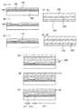
まず、第1の基板100上に剥離層102を形成する(図1(A−1)を参照)。剥離層102は単層であってもよいし、積層に形成しても良い。本実施の形態では、剥離層102は積層構造を有し、第1の剥離層104上に第2の剥離層106が形成されている。First, the
剥離層102は、スパッタリング法を用いて、タングステン、モリブデン、チタン、タンタル、ニオブ、ニッケル、コバルト、ジルコニウム、亜鉛、ルテニウム、ロジウム、パラジウム、オスミウム、イリジウム及び珪素から選択された元素、又はこれらの元素を主成分とする合金材料、又はこれらの元素を主成分とする化合物材料からなる層を、単層で、又は複数の層を積層して形成する。珪素を含む層の結晶構造は、非晶質、微結晶、多結晶のいずれの場合でもよい。The
剥離層102が単層構造の場合には、好ましくは、タングステン、モリブデン、又はタングステンとモリブデンの混合物を含む層を形成する。または、タングステンの酸化物若しくはタングステンの酸化窒化物を含む層、モリブデンの酸化物若しくはタングステンの酸化窒化物を含む層、又はタングステンとモリブデンの混合物の酸化物若しくは酸化窒化物を含む層を形成する。なお、タングステンとモリブデンの混合物とは、例えば、タングステンとモリブデンの合金に相当する。In the case where the
剥離層102が積層構造の場合には、好ましくは、1層目として金属層を形成し、2層目として金属酸化物層を形成する。代表的には、1層目として、タングステン、モリブデン、又はタングステンとモリブデンの混合物を含む層を形成し、2層目として、これらの酸化物、窒化物、酸化窒化物又は窒化酸化物を含む層を形成する。In the case where the
剥離層102として、1層目に金属層、2層目に金属酸化物層の積層構造を形成する場合には、金属層としてタングステンを含む層を形成し、その上に金属酸化物からなる絶縁層を形成すると、タングステンを含む層と絶縁層との界面に金属酸化物層としてタングステンの酸化物を含む層が形成されるため、これを活用してもよい。さらには、金属層の表面に対して、熱酸化処理、酸素プラズマ処理、又はオゾン水等の酸化力の強い溶液による処理等を行って金属酸化物層を形成してもよい。例えば、タングステン上に酸化シリコンを成膜して、タングステンと酸化シリコンとの間にタングステン酸化物を形成しても良い。しかし、タングステンの酸化物と酸化シリコンとは密着し難く、剥離には有利であるが、作製工程中において意図せず剥離してしまう可能性がある。一方、タングステンと酸化シリコンとの間にタングステン窒化物を形成すると、作製工程中における意図しない剥離を防止することはできるが、剥離し難くなるという問題がある。そのため、剥離層と窒化シリコンとの間に設ける層は、実施者の意思に応じて適宜設定するとよい。In the case of forming a stacked structure of a metal layer as the first layer and a metal oxide layer as the second layer as the
更には、剥離層102として、1層目に金属層、2層目に金属窒化物層又は金属酸化窒化物層を形成してもよい。代表的には、1層目にタングステンを含む層を形成し、2層目に、窒化タングステン層又は酸化窒化タングステン層を形成すればよい。Further, as the
剥離層102の膜厚は、本実施の形態では、第1の剥離層104としてタングステン膜を30nmで、第2の剥離層106として酸化シリコン膜を300nmで形成する。第1の剥離層104及び第2の剥離層106は、スパッタリング法又はCVD法等により形成することができる。第1の剥離層104及び第2の剥離層106は、スパッタリング法により形成することが好ましい。In this embodiment mode, the
なお、第1の剥離層104としてタングステン膜を形成し、第2の剥離層106としてCVD法により酸化シリコンを形成する場合には、第1の剥離層104であるタングステン膜を成膜した直後にN2Oプラズマ処理を行うことが好ましい。Note that in the case where a tungsten film is formed as the
次に、剥離層102の表面に段差を設ける。具体的には、所望の半導体素子の下のSiO2膜の膜厚を保持し、前記所望の半導体素子が形成されていない領域はSiO2膜の膜厚を薄くする。パターンの形成にはレジストマスクを用いる。所望のパターンを有するレジストマスクが形成された状態で、第2の剥離層106すなわち酸化シリコン膜をエッチングする。このエッチングの方法は、ドライエッチング又はウエットエッチングのいずれでも良い。また酸化シリコン膜は、後に可撓性基板等に剥離転置可能な膜厚の範囲で薄くする。ここでは膜厚200nmまでエッチングする。Next, a step is provided on the surface of the
次に、剥離層108上に、絶縁膜である第1の接合層110を形成する。第1の接合層110は表面が親水性を有する材料により設ける。第1の接合層110としては、酸化シリコン膜が適している。特にシランガス、ジシランガス、トリシランガス又は有機シランガス等のシラン系ガスを用いて化学気相成長法により作製される酸化シリコン膜が好ましい。シランガスを用いる場合、二酸化窒素又は一酸化二窒素との混合ガスを用いることが好適である。有機シランガスとしては、珪酸エチル(TEOS:化学式Si(OC2H5)4)、トリメチルシラン(TMS:(CH3)3SiH)、テトラメチルシクロテトラシロキサン(TMCTS)、オクタメチルシクロテトラシロキサン(OMCTS)、ヘキサメチルジシラザン(HMDS)、トリエトキシシラン(SiH(OC2H5)3)又はトリスジメチルアミノシラン(SiH(N(CH3)2)3)等のシリコン含有化合物を用いることができる。化学気相成長法としては、プラズマCVD、熱CVD又は光CVDを用いればよい。Next, a
なお、本明細書中において、親水性とは、固体表面における水の接触角により定義される。接触角とは、滴下したドットの淵における、形成面と液滴の接線がなす角度θのことを指す(図12を参照)。固体表面に水を滴下した際の接触角が0°以上90°以下であるときには該固体表面は親水性であるとし、90°以上180°以下であるときには該固体表面は撥水性であるとする。In the present specification, hydrophilicity is defined by the contact angle of water on the solid surface. The contact angle refers to an angle θ formed by the tangent line between the formation surface and the droplet in the mist of the dropped dot (see FIG. 12). When the contact angle when water is dropped on the solid surface is 0 ° or more and 90 ° or less, the solid surface is hydrophilic, and when the contact angle is 90 ° or more and 180 ° or less, the solid surface is water repellent. .
上記の、親水性表面を有する第1の接合層110は50nm以上500nm以下の厚さで設けるとよい。前記厚さは、剥離層102の表面の段差を十分埋める大きさが必要であり、すなわち段差に応じた膜厚とする。The
前記第1の接合層110は、凹凸を有している。表面に凹凸を有すると、後の工程にて二つの基板上の接合層を接合する際に、接合層間の接触面積が小さくなり、十分な接合強度を確保することが困難である。そのため、第1の接合層110を平坦化する。The
第1の接合層110の平坦化は、剥離層の全面を均一に平坦化できる方法により行うとよい。このような工程として、例えば、CMPや逆スパッタリング法が挙げられる。但し、これに限定されず、物理的エッチング方法又は化学的エッチング方法等、平坦性を高めることのできる処理であれば、処理方法は特に問わない。The
上記第1の接合層110の平坦化後の膜厚は、所望する素子の形成される領域では、5nm以上あることが好ましい。膜厚に上限は無いものの、スループットを考慮し、好適には100nm以下とする。The thickness of the
上記のように第1の基板100上に薄膜を形成する一方で、半導体基板200にも処理を行う。While the thin film is formed on the
半導体基板200には、まず表面から一定の深さの位置に、損傷層202を形成する。損傷層202は、清浄化された半導体基板200の表面から、電界で加速されたイオンを所定の深さに注入することで形成される。イオンの注入では、第1の基板100上に形成する半導体層(以下、LTSS層という。)の厚さを考慮して加速電圧等を調整する。LTSS層の厚さは、5nm以上500nm以下、好ましくは10nm以上200nm以下である。損傷層202の形成には、水素、不活性ガス又はハロゲンを用いる。不活性ガスとしてはヘリウムが挙げられ、ハロゲンとしてはフッ素が挙げられる。First, a
損傷層202の形成ではイオンを高ドーズ条件にて注入するため、半導体基板200の表面が粗くなる場合がある。この、表面の荒れを防ぐためには、イオン注入される表面に、保護膜を設けておくとよい。この保護膜は、酸化シリコン膜、窒化シリコン膜又は窒化酸化シリコン膜等により0.5nm以上200nm以下の厚さで設ければよい。In forming the damaged
なお、ここでイオン注入時の高ドーズ条件とは、本発明を実施する者が目的に応じて適宜設定すればよい。このドーズ条件により、損傷層202が半導体基板表面からどれだけの深さの位置に形成されるかが決定される。例えば、加速電圧を60kV、ドーズ量を2.0×10cm−2とすると、半導体基板表面から約150nmの深さの位置に損傷層202が形成される。Here, the high dose condition at the time of ion implantation may be appropriately set according to the purpose by a person who implements the present invention. This dose condition determines how deep the damaged
次に、半導体基板表面に、下地絶縁膜203を形成する。下地絶縁膜203としては、酸化シリコン膜、窒化シリコン膜または酸化窒化シリコン膜(SiOxNy)等の絶縁膜を用いる。代表的な一例は下地絶縁膜203として2層構造から成り、SiH4、及びN2Oを反応ガスとして成膜される酸化窒化シリコン膜を100〜150nm、SiH4、NH3、及びN2Oを反応ガスとして成膜される窒化酸化シリコン膜を50〜100nm、の厚さに積層形成する構造が採用される。また、下地絶縁膜203の一層として膜厚10nm以下の窒化シリコン膜(SiN膜)、或いは窒化酸化シリコン膜(SiNxOy膜(X>Y))を用いることが好ましい。また、窒化シリコン膜、酸化窒化シリコン膜、窒化酸化シリコン膜、を順次積層した3層構造を用いてもよい。下地絶縁膜203は基板からTFTにナトリウム等の可動イオンが侵入することを防ぐためのブロッキング層として機能する。また、下地絶縁膜203はバッファ層として機能する。
Next, a
次に、第1の基板100と接合する面に、表面の平坦性が高い絶縁膜である第2の接合層210を形成する(図1(B−2)を参照)。第2の接合層210は、酸化シリコン膜により形成することが好ましい。酸化シリコン膜としては上述のように有機シランガスを用いて化学気相成長法により作製される酸化シリコン膜が好ましく、シランガス、ジシランガス又はトリシランガス等シラン系ガスを用いて、化学気相成長法により作製される酸化シリコン膜を適用してもよい。化学気相成長法による成膜では、半導体基板200に形成した損傷層202から脱ガスが起こらない温度(例えば、350℃以下)とする。また、単結晶若しくは多結晶半導体基板からLTSS層を剥離する熱処理には、成膜温度よりも高い熱処理温度が適用される。Next, a
なお、化学気相成長法としては、プラズマCVD法、熱CVD法又は光CVD法を用いれば良い。特にTEOSとO2によりプラズマCVDを用いて、又はSiH4とNO2により熱CVD法を用いて形成すると、接合層に適した平坦な酸化シリコン膜を低温(350℃以下)で形成する事ができるため、好ましい。Note that a plasma CVD method, a thermal CVD method, or a photo CVD method may be used as the chemical vapor deposition method. In particular, when a plasma CVD method using TEOS and O2 or a thermal CVD method using SiH4 and NO2 is used, a flat silicon oxide film suitable for the bonding layer may be formed at a low temperature (350 ° C. or lower). This is preferable because it is possible.
また、第2の接合層210となる酸化シリコン膜は、オゾン水と過酸化水素とを含む薬液で形成してもよいし、オゾン水で形成しても良い。その場合には、膜厚は0.5nm以上5nm以下で良い。また、接合層は水素又はフッ素で終端した半導体表面であってもよい。Further, the silicon oxide film to be the
なお、第1の接合層110と半導体基板200との接合強度に問題がなければ、第2の接合層210を形成することなく、第1の接合層110と半導体基板200とを直接接合しても良い。Note that if there is no problem in the bonding strength between the
同様に、剥離層102と第2の接合層210との接合強度に問題がなければ、第1の接合層110を形成することなく、剥離層102と第2の接合層210とを直接接合しても良い。Similarly, if there is no problem in the bonding strength between the
つまり、接合強度に問題がなければ、必ずしも第1の基板100上と半導体基板200上の双方に接合層を形成しなくともよい。接合層を形成しないことで、半導体装置の作製工程において、スループットを向上させることができる。That is, if there is no problem in bonding strength, the bonding layer is not necessarily formed on both the
次に、第1の基板100上に形成された第1の接合層110と、半導体基板200上に形成された第2の接合層210とを密接させて接合する(図1(D)を参照)。これにより、接合形成層112が形成される。第1の接合層110と第2の接合層210とを密接させることで、室温でも接合することが可能である。より強固に接合するためには、第1の基板100と半導体基板200を押圧すれば良い。更には、熱処理を加えることが好ましい。加圧した状態で熱処理をしても良い。加圧した状態で熱処理を行うことで、第1の接合層110と第2の接合層210との接合がより強固になるため、接合層間の剥離を低減することができ、歩留まりが向上する。また、得られる半導体装置の信頼性が向上する。Next, the
接合を形成する面が異種材料である場合、低温で接合する際には接合を形成する面を清浄化する。清浄化した、第1の接合層110と第2の接合層210とを密接させると、表面間引力により接合形成層112が形成される。清浄化した表面を親水性表面とするためには、多数の水酸基を付着させればよい。例えば、第1の接合層110又は第2の接合層210の表面を、酸素プラズマ処理若しくはオゾン処理することで、これらの表面を親水性にすることができる。このように表面を親水性にする処理を加えると、表面の水酸基が作用して水素結合により強固な接合が形成される。When the surface on which the bond is formed is made of a different material, the surface on which the bond is formed is cleaned when bonding at a low temperature. When the cleaned
また、良好な接合を形成するために、接合を形成する面を活性化しておいても良い。例えば、接合を形成する面に原子ビーム若しくはイオンビームを照射する。原子ビーム若しくはイオンビームを利用する場合、アルゴン等の、不活性ガス中性原子ビーム若しくは不活性ガスイオンビームを照射することができる。イオンビームの照射により、第1の接合層110又は第2の接合層210の表面に未結合手が露出し、非常に活性な表面が形成される。または、プラズマ照射若しくはラジカル処理を行ってもよい。接合を形成する面に対してこのような表面処理を行うことにより、200℃乃至400℃程度の温度で、第1の接合層110と第2の接合層210が異種材料であっても、接合形成層112を容易に形成することができる。表面を活性化して接合する方法は、当該表面を高度に清浄化しておくことが要求されるので、真空中で行うことが好ましい。また、更に好ましくは高真空中で行う。Further, in order to form a good bond, the surface on which the bond is formed may be activated. For example, an atomic beam or an ion beam is irradiated to the surface on which the junction is formed. When an atomic beam or an ion beam is used, an inert gas neutral atom beam or inert gas ion beam such as argon can be irradiated. By irradiation with the ion beam, dangling bonds are exposed on the surface of the
接合形成層112の接合強度を高めるためには、接合後に加熱処理又は加圧処理を行うことが好ましい。接合形成層112が室温にて貼り合わせられた場合には、接合後に熱処理を行うことが、特に好ましい。加熱処理又は加圧処理を行うことで、接合を形成する面において接合に寄与する主な結合を、水素結合から共有結合に変換することができ、接合強度が向上する。加熱処理の温度は、第1の基板100の耐熱温度以下で行う。加圧処理においては、接合面に対して垂直な方向に圧力を加える。ここで加える圧力は、第1の基板100と半導体基板200の機械的強度を考慮して決定する。In order to increase the bonding strength of the
次に、半導体基板200が貼り合わせられた第1の基板100に熱処理を行い、損傷層202内の任意の位置を劈開面として、半導体基板200を第1の基板100から剥離する。剥離には物理的手段を用いればよい。熱処理の温度は第1の接合層110及び第2の接合層210の成膜温度以上、第1の基板100の耐熱温度以下で行うことが好ましい。例えば、400℃乃至600℃の熱処理を行うことにより、損傷層202に形成された微小な空洞の体積変化が起こり、損傷層202に沿って劈開することが可能となる。接合形成層112は第1の基板100と接合しているので、第1の基板100上には半導体基板200と同じ結晶性のLTSS層が残存することとなる。Next, heat treatment is performed on the
なお、物理的手段とは、力学的手段または機械的手段を指し、何らかの力学的エネルギー(機械的エネルギー)を変化させる手段を指しており、その手段は、代表的には機械的な力を加えること(例えば、人間の手や把治具で引き剥がす処理や、ローラーを回転させながら分離する処理)である。The physical means refers to mechanical means or mechanical means, and means means for changing some mechanical energy (mechanical energy). The means typically applies mechanical force. (For example, a process of peeling with a human hand or a grip jig, or a process of separating while rotating a roller).
LTSS層116は、上記剥離工程後にCMP等を用いて、平坦化及び薄膜化されることが好ましい。例えば、単結晶半導体基板の所定の深さに、水素、ヘリウムに代表される不活性ガス、又はフッ素に代表されるハロゲンのイオンを注入し、その後熱処理を行って表層の単結晶シリコン層を剥離するイオン注入剥離法で形成することができる。また、ポーラスシリコン上に単結晶シリコンをエピタキシャル成長させ、ポーラスシリコン層をウオータージェットで劈開して剥離する方法を適用しても良い。LTSS層116の厚さは5nm乃至500nm、好ましくは10nm乃至200nmである。なお、本発明はこれに限定されず、LTSS層の平坦化及び薄膜化は逆スパッタリング法にて行ってもよい。更には、CMPと逆スパッタリング法を併用して平坦化及び薄膜化を行ってもよい。The
また、損傷層202を劈開面として半導体基板200を剥離する前に、剥離を容易に行うためのきっかけを形成してもよい。さらには、半導体基板200を剥離する際、第1の基板100又は半導体基板200の少なくとも一方の表面に光又は熱により剥離可能な粘着シートを設けて、第1の基板100及び半導体基板200のいずれかを固定し、他方を引き剥がすと、剥離が更に容易になる。このとき、第1の基板100又は半導体基板200の他方に支持部材を設けることで、容易に引き剥がすことができる。Further, before the
なお、図示していないが、LTSS層116と接合形成層114の間にバリア層を設けても良い。バリア層は、第1の基板100として用いられるガラス基板からアルカリ金属若しくはアルカリ土類金属のような可動イオン不純物が拡散してLTSS層116が汚染されることを防止できる材質の膜を形成する。また、第1の剥離層104又は第2の剥離層106からの不純物の拡散を防止することもできる。バリア層として、例えば、窒素含有絶縁層を用いることができる。窒素含有絶縁層は窒化シリコン膜、窒化酸化シリコン膜若しくは酸化窒化シリコン膜を単層で、又は積層して形成することができる。例えば、LTSS層116側から酸化窒化シリコン膜と、窒化酸化シリコン膜と、を積層して形成することで、窒素含有絶縁膜によりバリア層を設けることができる。Although not shown, a barrier layer may be provided between the
なお、ここで酸化窒化シリコン膜とは、その組成として、窒素よりも酸素の含有量が多いものであって、濃度範囲として酸素が55〜65原子%、窒素が1〜20原子%、Siが25〜35原子%、水素が0.1〜10原子%の範囲で含まれるものをいう。また、窒化酸化シリコン膜とは、その組成として、酸素よりも窒素の含有量が多いものであって、濃度範囲として酸素が15〜30原子%、窒素が20〜35原子%、Siが25〜35原子%、水素が15〜25原子%の範囲で含まれるものをいう。Here, the silicon oxynitride film has a composition with a higher oxygen content than nitrogen, and the concentration ranges are oxygen of 55 to 65 atomic%, nitrogen of 1 to 20 atomic%, and Si. 25 to 35 atomic%, and hydrogen is included in the range of 0.1 to 10 atomic%. The silicon nitride oxide film has a composition containing more nitrogen than oxygen, and the concentration ranges of oxygen are 15 to 30 atomic%, nitrogen is 20 to 35 atomic%, and Si is 25 to 25%. 35 atomic% and hydrogen are included in the range of 15 to 25 atomic%.
なお、本発明は上記の説明に限定されない。第2の接合層210が不要な場合には特に形成しなくても良い(図3を参照)。なお、接合層が不要な場合とは、接合層を形成しなくとも、貼り合わせ面と被貼り合わせ面が良好に貼り合わせられる場合をいう。第1の接合層110及び第2の接合層210の一方のみを形成し、又は双方を形成しないことで、工程が削減され、スループットが向上する。The present invention is not limited to the above description. When the
以上説明したように、本発明により素子領域211と、その間すなわち素子間領域212との間に段差が設けられた剥離層により、可撓性基板への転写時の歩留まりを向上させることができる(図1〜図4参照)。As described above, according to the present invention, the yield at the time of transfer to a flexible substrate can be improved by the separation layer provided with a step between the
(実施の形態2)
本発明は、実施の形態1にて説明した形態に限定されず、例えば、剥離層を半導体基板上に形成しても良い。このような形態について、以下に説明する。なお、重複する点については、説明を省略する。(Embodiment 2)
The present invention is not limited to the embodiment described in
図4は、剥離層を半導体基板上に形成する形態の一例を示す。FIG. 4 shows an example of a mode in which a release layer is formed on a semiconductor substrate.
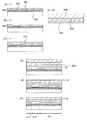
まず、半導体基板200に実施の形態1と同様にドープを行って損傷層202を形成する(図4(A−2)を参照)。First, the damaged
次に、損傷層202が形成された半導体基板200上に、実施の形態1と同様に剥離層102を形成する(図4(B−2)を参照)。Next, the
次に、剥離層102に段差を設け、さらに絶縁膜を形成する。Next, a step is provided in the
次に、絶縁膜を平坦化し、第2の接合層210を形成する。なお、平坦化はCMP法により行うことが好ましい(図4(C−2)を参照)。Next, the insulating film is planarized and the
半導体基板200に処理を行う一方で、第1の基板100上に実施の形態1と同様に、表面の平坦性が高い絶縁膜である第1の接合層110を形成する(図4(A−1)を参照)。While the
以上のように処理を行った第1の基板100と、半導体基板200と、を貼り合わせる。つまり、実施の形態1と同様に、第1の接合層110と第2の接合層210とを接合させ、接合形成層112を形成することができる(図4(D)を参照)。The
次に、半導体基板200を損傷層で剥離することで、第1の基板上に半導体層を形成する(図4(E)を参照)。更には、半導体層を平坦化することで、LTSS層116を形成する。Next, the
なお、本発明は上記の説明に限定されない。第1の接合層110が不要な場合には特に形成しなくても良い(図5を参照)。なお、接合層が不要な場合とは、接合層を形成しなくとも、貼り合わせ面と被貼り合わせ面が良好に貼り合わせられる場合をいう。第1の接合層110及び第2の接合層210の一方のみを形成し、又は双方を形成しないことで、工程が削減され、スループットが向上する。The present invention is not limited to the above description. When the
尚、剥離層を第1の剥離層、第2の剥離層の順で形成する2層構造とし、第1の剥離層と、第2の剥離層との間で剥離する構造の場合、実施の形態1では、剥離層2の一部が残り、実施の形態2では、剥離層1の一部が残ることとなる。所望の構造が形成されるように、いずれかを選択することができる。
(実施の形態3)
本発明は、実施の形態1および実施の形態2にて説明した形態にて好適に用いられるが、接合層および半導体基板を用いず、第1の基板100上に直接所望の半導体素子を形成しても良い。このような形態について、図5を用い以下に説明する。なお、重複する点については、説明を省略する。In the case of a two-layer structure in which the release layer is formed in the order of the first release layer and the second release layer, and in the case of a structure that peels between the first release layer and the second release layer, In
(Embodiment 3)
The present invention is preferably used in the modes described in the first and second embodiments, but a desired semiconductor element is formed directly on the
まず、第1の基板100上に実施の形態1と同様に、剥離層102を形成する。First, the
次に、剥離層102に段差を設け、剥離層108を形成し、さらに絶縁膜110を形成する。Next, a step is provided in the
次に、絶縁膜を平坦化し、さらに下地絶縁膜203を形成する。Next, the insulating film is planarized and a
下地絶縁膜203は、酸化シリコン、窒化シリコン、窒化酸化シリコン、酸化窒化シリコン等の絶縁材料の単層膜または積層膜で形成することができる。これらの絶縁膜はCVD法、スパッタ法で形成することができる。下地絶縁膜203を形成することで、半導体膜の基板側の界面準位密度を低減すること、基板からアルカリ金属などの汚染物質が半導体膜に侵入することを防ぐ、などの効果がある。The base
その上に、半導体膜206を形成する。半導体膜206は、非単結晶半導体膜であり、多結晶半導体で形成されたものが好ましい。半導体材料としては、シリコンが好ましく、その他、シリコンゲルマニウムおよびゲルマニウムを用いることができる。これらは公知の手段(スパッタ法、LPCVD法、またはプラズマCVD法等)で成膜することによって得る。A
以上の工程により、実施の形態1あるいは実施の形態2のように、必要な耐熱性を有する基板上に剥離層を形成し、該剥離層上に半導体層を形成することができる。本実施の形態で形成される半導体層は非単結晶であり、実施の形態1あるいは実施の形態2の工程にて形成されるものより、若干半導体層の結晶性は低くなるものの、より少ない工程を経るためスループットの向上を見込むことができる。Through the above steps, as in
(実施の形態4)
実施の形態1、又は実施の形態2、実施の形態3にて説明したように、SOI基板を作製し、該SOI基板を用いて半導体装置を作製することができる。本実施の形態では、本発明を適用した薄膜集積回路の作製方法について、図面を参照してより詳細に説明する。尚、本実施の形態では、LTSS層及び非単結晶半導体膜は、半導体膜と称する。(Embodiment 4)
As described in
図7(A)は、実施の形態1、又は実施の形態2、実施の形態3にて説明したように作製したSOI基板を示す。但し、素子領域211部分のみを表している。まず、SOI基板の半導体膜214を所望の形状となるようパターンを形成する(図7(B)を参照)。パターンの形成にはレジストマスクを用いる。所望のパターンを有するレジストマスクが形成された状態で、半導体膜214をエッチングし、半導体膜216を形成する。このときのエッチング条件は、LTSS層に対するエッチングレートが高く、接合形成層112に対するエッチングレートの低い条件とすればよく、ドライエッチング又はウエットエッチングのいずれかを選択する。FIG. 7A illustrates an SOI substrate manufactured as described in
次に、ゲート絶縁膜120、ゲート電極層122及びサイドウォール124を順次形成し、半導体膜216にソース領域又はドレイン領域126及びLDD領域128を形成する(図7(C)を参照)。Next, a
ゲート絶縁膜120は、酸化シリコン、窒化シリコン、酸化窒化シリコン又は窒化酸化シリコン等により形成する。形成には、CVD法、スパッタリング法、プラズマCVD法等を用いればよい。膜厚は、5nm以上200nm以下とする。なお、ゲート絶縁膜120は、図示する構造に限定されず、全面に形成されていても良い。The
ゲート電極層122は、CVD法、スパッタリング法又は液滴吐出法等を用いて形成することができる。ゲート電極層122は、タンタル、タングステン、チタン、モリブデン、アルミニウム、銅から選ばれた元素又は前記元素を主成分とする合金材料若しくは化合物材料で形成すればよい。ゲート電極層122にアルミニウムを使用する際には、タンタルを添加して合金化したAl−Ta合金を用いるとヒロックが抑制される。また、ネオジムを添加して合金化したAl−Nd合金を用いると、ヒロックが抑制されるだけでなく、抵抗の低い配線を形成することができる。そのため、Al−Ta合金又はAl−Nd合金を用いることが好ましい。また、リン等の不純物元素をドーピングした多結晶シリコンに代表される半導体膜やAgPdCu合金を用いてもよい。また、単層でも積層でもよい。例えば、窒化チタン膜とモリブデン膜から構成される2層の積層構造又は膜厚50nmのタングステン膜と膜厚500nmのアルミニウムとシリコンの合金膜と膜厚30nmの窒化チタン膜を積層した3層の積層構造としてもよい。また、3層の積層構造とする場合、第1の導電膜のタングステンに代えて窒化タングステンを用いてもよいし、第2の導電膜のアルミニウムとシリコンの合金膜に代えてアルミニウムとチタンの合金膜を用いてもよいし、第3の導電膜の窒化チタン膜に代えてチタン膜を用いてもよい。ゲート電極層122は単層で形成してもよいし、積層で形成してもよい。例えば、主成分がモリブデンである膜により形成すればよい。The
ゲート電極層122の側面にはサイドウォール124を設ける。サイドウォール124は、絶縁膜を全面に形成し、選択的にエッチングすることにより行う。なお、絶縁膜種はゲート絶縁膜120と同様である。
ソース領域又はドレイン領域126、及びLDD領域128は、一導電型の不純物元素を添加することにより形成する。ソース領域又はドレイン領域126は一導電型の不純物が高濃度に導入された高濃度不純物領域であり、LDD領域128は一導電型の不純物が低濃度に導入された高濃度不純物領域である。濃度の異なる領域を作り分けるためには、低濃度不純物領域を、絶縁膜を介したドープにより形成し、高濃度不純物領域をベアドープにより形成すればよい。または、低濃度不純物領域及び高濃度不純物領域の双方に低濃度に不純物を導入し、その後、高濃度不純物領域にのみ不純物を高濃度に導入してもよい。なお、LDD領域とは半導体層が多結晶シリコン膜により形成されているTFTにおいて、信頼性の向上を目的として形成される領域である。半導体層が多結晶シリコンであるTFTにおいてオフ電流を抑えることは重要であり、特に、画素回路などのアナログスイッチとして用いる場合には十分に低いオフ電流が要求される。しかし、ドレイン接合部の逆バイアス強電界により、オフ時にも欠陥を介するリーク電流が存在する。LDD領域により、ドレイン端近傍の電界を緩和するため、オフ電流を低減させることができる。また、ドレイン接合部の逆バイアス電界をチャネル形成領域とLDD領域の接合部と、LDD領域とドレイン領域の接合部とに分散させることができ、電界が緩和されるため、リーク電流が低減される。その後アニールを行うことで、不純物の活性化を行う。The source or drain
次に、絶縁膜130を形成し、所望の位置に開口部を形成する。絶縁膜130に設けられた開口部を介して、半導体膜216のソース領域及びドレイン領域に接続されるように、ソース電極及びドレイン電極を形成する。その後、絶縁膜134を形成する(図7(D)を参照)。なお、絶縁膜134は必要のない場合には設けなくても良い。Next, the insulating
絶縁膜130を選択的に形成する。絶縁膜130はポリイミドやアクリル等に代表される有機材料からなる膜を、スピンコート法等により形成すればよい。パターンの形成に際しては、ソース領域及びドレイン領域126を露出するように開口部を形成する。なお、酸化シリコン膜、窒化シリコン膜、酸化窒化シリコン膜、又は窒化酸化シリコン膜のような無機材料からなる膜上に有機材料からなる膜を形成してもよい。または、これらの無機材料のみで形成してもよい。An insulating
次に、絶縁膜134を第2の基板136に固着する(図8(E)を参照)。第2の基板はすなわち可撓性基板が有効であり、この材料としては、PET(ポリエチレンテレフタレート)、PEN(ポリエチレンナフタレート)、PES(ポリエーテルスルホン)、ポリプロピレン、ポリプロピレンサルファイド、ポリカーボネート、ポリエーテルイミド、ポリフェニレンサルファイド、ポリフェニレンオキサイド、ポリサルフォン、ポリフタールアミド等からなるプラスチック基板または繊維質の材料からなる紙がある。Next, the insulating
また、第2の基板136としては、プリプレグを用いることで、後に作製されるSOI基板や半導体装置の点圧、線圧による破壊を防ぐことが可能である。プリプレグの代表例としては、ポリビニルアルコール系繊維、ポリエステル系繊維、ポリアミド系繊維、ポリエチレン系繊維、アラミド系繊維、ポリパラフェニレンベンゾビスオキサゾール繊維、ガラス繊維、または炭素繊維等の繊維体に、エポキシ樹脂、不飽和ポリエステル樹脂、ポリイミド樹脂又はフッ素樹脂等のマトリックス樹脂を有機溶剤で希釈したワニスを含浸させた後、乾燥して有機溶剤を揮発させてマトリックス樹脂を半硬化させたものである。In addition, by using a prepreg as the
また、第2の基板136としては、アルミノシリケートガラス、アルミノホウケイ酸ガラス又はバリウムホウケイ酸ガラスのような電子工業用に使われる各種ガラス基板を用いることができる。As the
次に、剥離層102をきっかけとして、第1の基板100から薄膜集積回路を剥離する。剥離は、加熱処理又はウエットエッチング等を用いればよい。Next, the thin film integrated circuit is peeled from the
この剥離が問題なく行えればよいが、工程の熱処理条件によっては、工程中のピーリング等を避けるため、剥離層をある程度強固にする必要がある。このためやむなく、剥離工程時に、基板面内のいずれかに剥離不良、クラックなどの欠陥が残ってしまうことがある。この条件時について、図8(F)で説明する。It is sufficient that this peeling can be performed without any problem. However, depending on the heat treatment conditions of the process, it is necessary to make the peeling layer somewhat strong in order to avoid peeling in the process. For this reason, it is unavoidable that defects such as defective peeling and cracks may remain in any part of the substrate surface during the peeling process. This condition will be described with reference to FIG.
図8(F)では、素子領域210と素子間領域212との境界付近を、剥離層の厚さの違いで説明している。剥離層の薄い素子間領域212は、素子領域210に比べて、剥離しにくくなっている。そのため、素子間領域212では耐熱性基板側に剥離層残渣218が残る、あるいは第2の基板側に転置された層にクラック220が発生する可能性がある。しかしながら素子領域210にはこれを避けることが出来る。そのため、素子の歩留まりを上げることができる。In FIG. 8F, the vicinity of the boundary between the
以上のように、半導体装置に設けられた薄膜集積回路が有するトランジスタを形成することができるが、本実施の形態は一例に過ぎない。即ち、本発明は本実施の形態に限定されず、実施の形態1又は実施の形態2にて説明したSOI基板を用いて作製する、如何なるトランジスタにも適用することができる。As described above, a transistor included in a thin film integrated circuit provided in a semiconductor device can be formed; however, this embodiment is merely an example. In other words, the present invention is not limited to this embodiment mode, and can be applied to any transistor manufactured using the SOI substrate described in
(実施の形態5)
次に、実施の形態1、又は実施の形態2、実施の形態3を適用して作製したSOI基板を用いて作製した半導体装置の一例として、マイクロプロセッサ300を図9に示す。このマイクロプロセッサ300は、演算回路301(Arithmeticlogicunit。ALUともいう。)、演算回路制御部302(ALUController)、命令解析部303(InstructionDecoder)、割り込み制御部304(InterruptController)、タイミング制御部305(TimingController)、レジスタ306(Register)、レジスタ制御部307(RegisterController)、バスインターフェース308(BusI/F)、ROM309(ReadOnlyMemory)、及びROMインターフェース310(ROMI/F)を有する。(Embodiment 5)
Next, a microprocessor 300 is illustrated in FIG. 9 as an example of a semiconductor device manufactured using an SOI substrate manufactured by applying
バスインターフェース308を介してマイクロプロセッサ300に入力された命令は、命令解析部303に入力され、デコードされた後、演算回路制御部302、割り込み制御部304、レジスタ制御部307及びタイミング制御部305に入力される。演算回路制御部302、割り込み制御部304、レジスタ制御部307及びタイミング制御部305は、デコードされた命令に基づき各種制御を行う。具体的に、演算回路制御部302は、演算回路301の動作を制御するための信号を生成する。また、割り込み制御部304は、マイクロプロセッサ300のプログラム実行中に、外部の入出力装置や周辺回路からの割り込み要求を、その優先度やマスク状態から判断して処理する。レジスタ制御部307は、レジスタ306のアドレスを生成し、マイクロプロセッサ300の状態に応じてレジスタ306の読み出しや書き込みを行う。タイミング制御部305は、演算回路301、演算回路制御部302、命令解析部303、割り込み制御部304、レジスタ制御部307の動作のタイミングを制御する信号を生成する。例えば、タイミング制御部305は、基準クロック信号CLK1を元に、内部クロック信号CLK2を生成する内部クロック生成部を備えており、クロック信号CLK2を上記の各種回路に供給する。なお、図9に示すマイクロプロセッサ300は、その構成を簡略化して示した一例にすぎず、実際にはその用途によって多種多様な構成を備えることができる。An instruction input to the microprocessor 300 via the
このようなマイクロプロセッサ300は、可撓性を有する基板上に接合される工程の際、素子内へのクラックが抑えられるので、歩留まりの向上を図ることができる。In such a microprocessor 300, cracks in the element can be suppressed in the process of bonding onto a flexible substrate, so that the yield can be improved.
次に、非接触でデータの送受信を行うことのできる演算機能を備えた半導体装置の一例について図10を参照して説明する。図10は無線通信により外部装置と信号の送受信を行って動作するコンピュータ(以下、「RFCPU」という)の一例を示す。RFCPU311は、アナログ回路部312及びデジタル回路部313を有している。アナログ回路部312とは、共振容量を有する共振回路314、整流回路315、定電圧回路316、リセット回路317、発振回路318、復調回路319と、変調回路320を有している。デジタル回路部313は、RFインターフェース321、制御レジスタ322、クロックコントローラ323、CPUインターフェース324、CPU325、RAM326及びROM327を有している。Next, an example of a semiconductor device having an arithmetic function capable of transmitting and receiving data without contact will be described with reference to FIGS. FIG. 10 shows an example of a computer (hereinafter referred to as “RFCPU”) that operates by transmitting and receiving signals to and from an external device by wireless communication. The RFCPU 311 has an analog circuit portion 312 and a digital circuit portion 313. The analog circuit portion 312 includes a
このような構成のRFCPU311の動作は概略以下の通りである。アンテナ328が受信した信号は共振回路314により誘導起電力を生じさせる。誘導起電力は、整流回路315を経て容量部329に充電される。この容量部329はセラミックコンデンサーや電気二重層コンデンサーなどのキャパシタで形成されていることが好ましい。容量部329はRFCPU311と一体形成されている必要はなく、別部品としてRFCPU311を構成する絶縁表面を有する基板に取り付けられていれば良い。The operation of the RFCPU 311 having such a configuration is roughly as follows. A signal received by the antenna 328 causes an induced electromotive force by the
リセット回路317は、デジタル回路部313をリセットし、初期化する信号を生成する。例えば、電源電圧の上昇に遅延して立ち上がる信号をリセット信号として生成する。発振回路318は、定電圧回路316により生成される制御信号に応じて、クロック信号の周波数とデューティー比を変更する。ローパスフィルタで形成される復調回路319は、例えば振幅変調(ASK)方式の受信信号の振幅の変動を二値化する。変調回路320は、送信データを振幅変調(ASK)方式の送信信号の振幅の変動により送信する。変調回路320は、共振回路314の共振点を変化させることで通信信号の振幅を変化させている。クロックコントローラ323は、電源電圧又はCPU325における消費電流に応じてクロック信号の周波数とデューティー比を変更するための制御信号を生成する。電源電圧の監視は電源管理回路330が行う。The
アンテナ328からRFCPU311に入力された信号は復調回路319で復調された後、RFインターフェース321で制御コマンドやデータなどに分解される。制御コマンドは制御レジスタ322に格納される。制御コマンドには、ROM327に記憶されているデータの読み出し、RAM326へのデータの書き込み、CPU325への演算命令などが含まれている。CPU325は、CPUインターフェース324を介してROM327、RAM326及び制御レジスタ322にアクセスする。CPUインターフェース324は、CPU325が要求するアドレスより、ROM327、RAM326及び制御レジスタ322のいずれかに対するアクセス信号を生成する機能を有する。A signal input from the antenna 328 to the RFCPU 311 is demodulated by the
CPU325の演算方式は、ROM327にOS(オペレーティングシステム)を記憶させておき、起動とともにプログラムを読み出し実行する方式を採用することができる。また、専用回路で演算回路を構成して、演算処理をハードウェア的に処理する方式を採用することもできる。ハードウェアとソフトウェアを併用する方式では、専用の演算回路で一部の処理を行い、プログラムを用いて残りの演算をCPU325が実行する方式を適用することができる。As a calculation method of the
本発明を適用したSOI基板を用いた半導体装置を、可撓性を有する基板上に接合される工程の際、素子内へのクラックが抑えられるので、歩留まりの向上を図ることができる。In the process of bonding a semiconductor device using an SOI substrate to which the present invention is applied to a flexible substrate, cracks in the element are suppressed, so that yield can be improved.
以上のように、本発明を適用したSOI基板を用いてマイクロプロセッサ又はRFCPUを作製することができる。しかし、本実施の形態は一例に過ぎない。即ち、本発明は本実施の形態に限定されず、実施の形態1又は実施の形態2にて説明したSOI基板を用いて作製する、如何なる半導体装置にも適用することができる。As described above, a microprocessor or an RFCPU can be manufactured using an SOI substrate to which the present invention is applied. However, this embodiment is only an example. In other words, the present invention is not limited to this embodiment mode, and can be applied to any semiconductor device manufactured using the SOI substrate described in
(実施の形態6)
本発明を適用して作製したSOI基板を用いて表示パネルを作製することもできる。本実施の形態では、このような表示パネルについて説明する。(Embodiment 6)
A display panel can also be manufactured using an SOI substrate manufactured by applying the present invention. In this embodiment, such a display panel is described.
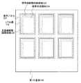
図11は実施の形態1、又は実施の形態2を適用し、第1の基板100として、大面積基板を用い、半導体基板200を貼り合わせて、第1の基板上にLTSS層116を形成する場合を示す。大面積基板からは複数の表示パネルを切り出すため、LTSS層116は、表示パネル331の形成領域に合わせて接合することが好ましい。単結晶半導体基板に比べて、表示パネルを形成する大面積基板は面積が大きいため、LTSS層116は図11のように分割して配置することが好ましい。表示パネル331は、走査線駆動回路領域332、信号線駆動回路領域333及び画素形成領域334を有し、これらの領域が含まれるようにLTSS層116を第1の基板100に接合する。尚、実施の形態3を適用した場合は半導体層を基板一面に形成できるので、この操作は不要である。FIG. 11 applies
図12は実施の形態1又は実施の形態2を適用して形成されたLTSS層、または実施の形態3を適用して形成された非単結晶半導体膜、の何れかを用いた半導体層により画素トランジスタ401が構成される発光表示パネルの画素の一例の断面図を示す。FIG. 12 illustrates a pixel using a semiconductor layer using either an LTSS layer formed by applying
図12(A)において、画素トランジスタ401は第1の電極402に接続され、第1の電極402上にはEL層403が形成され、EL層403上には第2の電極404が形成されている。図12(A)は、第1の基板100上に発光表示パネルを形成し、剥離した様子を示す。転置される第2の基板として、プラスチック基板405を用いている。なお、図12(A)では、第1の剥離層104と第2の剥離層106との境界にて剥離されているが、本発明はこれに限定されない。In FIG. 12A, a
図12(B)は、図12(A)において転置した発光表示パネルの下にプラスチック基板406を設けた構成を示す。このようにプラスチック基板406を設けることで、発光表示パネルの耐衝撃性等を高め、信頼性を向上させることができる。FIG. 12B illustrates a structure in which a
本発明を適用したSOI基板を用いて発光表示パネルを作製することができる。しかし、本実施の形態は一例に過ぎない。即ち、本発明は本実施の形態に限定されず、実施の形態1又は実施の形態2にて説明したSOI基板を用いて作製する、如何なる半導体装置にも適用することができる。A light-emitting display panel can be manufactured using an SOI substrate to which the present invention is applied. However, this embodiment is only an example. In other words, the present invention is not limited to this embodiment mode, and can be applied to any semiconductor device manufactured using the SOI substrate described in
このように、可撓性を有する大面積基板に本発明を適用した発光表示パネルを設けることも可能である。発光表示パネルは一つの装置あたりの面積が大きく、一箇所でも素子に欠損があると全体が不良になるが、本発明を適用し、これらを図1乃至図5に何れかにおける素子領域211にて形成することで、可撓性を有する基板上に接合される工程の際、素子内へのクラックが抑えられ、歩留まりの向上を図ることができる。In this manner, a light-emitting display panel to which the present invention is applied can be provided over a flexible large-area substrate. A light-emitting display panel has a large area per device, and if an element is defective even at one place, the whole becomes defective. However, the present invention is applied, and these are applied to the
尚、実施の形態4にて説明したマイクロプロセッサも同一基板上に形成すれば、表示パネル内にコンピュータの機能を搭載することもできる。同様に、非接触でデータの入出力が可能なディスプレイを作製することもできる。Note that if the microprocessor described in Embodiment 4 is also formed over the same substrate, the function of a computer can be mounted in the display panel. Similarly, a display capable of inputting and outputting data without contact can be manufactured.
100 第1の基板
102 剥離層
104 第1の剥離層
106 第2の剥離層
108 剥離層
110 第1の接合層
112 接合形成層
114 接合形成層
116 LTSS層
120 ゲート絶縁膜
122 ゲート電極層
124 サイドウォール
126 ドレイン領域
128 LDD領域
130 絶縁膜
134 絶縁膜
136 第2の基板
200 半導体基板
202 損傷層
203 下地層
206 半導体膜
210 接合層
211 素子領域
212 素子間領域
214 半導体膜
216 半導体膜
218 剥離層残渣
220 クラック
300 マイクロプロセッサ
301 演算回路
302 演算回路制御部
303 命令解析部
304 制御部
305 タイミング制御部
306 レジスタ
307 レジスタ制御部
308 バスインターフェース
309 ROM
310 ROMインターフェース
311 RFCPU
312 アナログ回路部
313 デジタル回路部
314 共振回路
315 整流回路
316 定電圧回路
317 リセット回路
318 発振回路
319 復調回路
320 変調回路
321 RFインターフェース
322 制御レジスタ
323 クロックコントローラ
324 CPUインターフェース
325 CPU
326 RAM
327 ROM
328 アンテナ
329 容量部
330 電源管理回路
331 表示パネル
332 走査線駆動回路領域
333 信号線駆動回路領域
334 画素形成領域
401 画素トランジスタ
402 電極
403 EL層
404 電極
405 プラスチック基板
406 プラスチック基板DESCRIPTION OF
310 ROM interface 311 RFCPU
312 Analog circuit unit 313
326 RAM
327 ROM
Claims (10)
Translated fromJapanese単結晶シリコン基板である半導体基板の表面から一定の深さに損傷層を形成し、該損傷層が形成された前記半導体基板の表面に、下地絶縁膜を形成し、前記下地絶縁膜上に、第2の接合層を形成する工程と、
前記第1の接合層と、前記第2の接合層とを貼り合わせて前記損傷層で剥離することで、前記第1の基板上に半導体層を形成し、前記半導体層を有する半導体素子を形成する工程と、
前記半導体素子を前記剥離層に設けられた前記段差から剥離することで可撓性基板である第2の基板上に転置する工程と、を有し、
前記剥離層が前記段差により厚くなっている領域に前記半導体素子が形成されることを特徴とする半導体装置の作製方法。Forming a release layer on a first substrate having a strain point of 750 ° C. or higher, providing a step in the release layer, and forming a first bonding layer filling the step on the release layer;
A damaged layer is formed at a certain depth from the surface of the semiconductor substrate which is a single crystal silicon substrate, a base insulating film is formed on the surface of the semiconductor substrate on which the damaged layer is formed, and the base insulating film is formed on the base insulating film. Forming a second bonding layer;
The first bonding layer and the second bonding layer are bonded to each other and separated by the damaged layer, whereby a semiconductor layer is formed on the first substrate and a semiconductor element having the semiconductor layer is formed. And a process of
Have a, a step of transposition to a second substrate is a flexible substrate by peeling the semiconductor element from the step provided on the releaselayer,
A method for manufacturing a semiconductor device, wherein the semiconductor element is formed in a region where the release layer is thick due to the step .
単結晶シリコン基板である半導体基板の表面から一定の深さに損傷層を形成し、該損傷層が形成された前記半導体基板の表面に、下地絶縁膜を形成する工程と、
前記第1の接合層と、前記下地絶縁膜とを貼り合わせて前記損傷層で剥離することで、前記第1の基板上に半導体層を形成し、前記半導体層を有する半導体素子を形成する工程と、
前記半導体素子を前記剥離層に設けられた前記段差から剥離することで可撓性基板である第2の基板上に転置する工程と、を有し、
前記剥離層が前記段差により厚くなっている領域に前記半導体素子が形成されることを特徴とする半導体装置の作製方法。Forming a release layer on a first substrate having a strain point of 750 ° C. or higher, providing a step in the release layer, and forming a first bonding layer filling the step on the release layer;
Forming a damaged layer at a certain depth from the surface of the semiconductor substrate which is a single crystal silicon substrate, and forming a base insulating film on the surface of the semiconductor substrate on which the damaged layer is formed;
A step of forming a semiconductor element having the semiconductor layer by forming a semiconductor layer on the first substrate by bonding the first bonding layer and the base insulating film and separating the first insulating layer from the damaged layer. When,
Have a, a step of transposition to a second substrate is a flexible substrate by peeling the semiconductor element from the step provided on the releaselayer,
A method for manufacturing a semiconductor device, wherein the semiconductor element is formed in a region where the release layer is thick due to the step .
前記半導体素子を前記剥離層に設けられた前記段差から剥離することで可撓性基板である第2の基板上に転置する工程と、を有し、
前記剥離層が前記段差により厚くなっている領域に前記半導体素子が形成されることを特徴とする半導体装置の作製方法。A damaged layer is formed at a certain depth from the surface of the semiconductor substrate, which is a single crystal silicon substrate, a base insulating film is formed on the surface of the semiconductor substrate on which the damaged layer is formed, and peeling is performed on the base insulating film. Forming a layer, providing a step in the release layer, and forming a first bonding layer on the release layer; a surface of the first substrate having a strain point of 750 ° C. or higher; and the first bonding Forming a semiconductor element having the semiconductor layer by forming a semiconductor layer on the first substrate by laminating the layer and peeling off the damaged layer; and
Have a, a step of transposition to a second substrate is a flexible substrate by peeling the semiconductor element from the step provided on the releaselayer,
A method for manufacturing a semiconductor device, wherein the semiconductor element is formed in a region where the release layer is thick due to the step .
前記第1の接合層はCMPにて平坦化されていることを特徴とする半導体装置の作製方法。In any one of Claims 1 thru | or 3,
The method for manufacturing a semiconductor device, wherein the first bonding layer is planarized by CMP.
単結晶シリコン基板である半導体基板の表面から一定の深さに損傷層を形成し、該損傷層が形成された前記半導体基板の表面に、下地絶縁膜を形成し、前記下地絶縁膜上に剥離層を形成し、前記剥離層に段差を設け、前記剥離層上に前記段差を埋める第2の接合層を形成する工程と、
前記第1の接合層と、前記第2の接合層とを貼り合わせて前記損傷層で剥離することで、前記第1の基板上に半導体層を形成し、前記半導体層を有する半導体素子を形成する工程と、
前記半導体素子を前記剥離層に設けられた前記段差から剥離することで可撓性基板である第2の基板上に転置する工程と、を有し、
前記剥離層が前記段差により厚くなっている領域に前記半導体素子が形成されることを特徴とする半導体装置の作製方法。Forming a first bonding layer on a first substrate having a strain point of 750 ° C. or higher;
A damaged layer is formed at a certain depth from the surface of the semiconductor substrate, which is a single crystal silicon substrate, a base insulating film is formed on the surface of the semiconductor substrate on which the damaged layer is formed, and peeling is performed on the base insulating film. Forming a layer, providing a step in the release layer, and forming a second bonding layer filling the step on the release layer;
The first bonding layer and the second bonding layer are bonded to each other and separated by the damaged layer, whereby a semiconductor layer is formed on the first substrate and a semiconductor element having the semiconductor layer is formed. And a process of
Have a, a step of transposition to a second substrate is a flexible substrate by peeling the semiconductor element from the step provided on the releaselayer,
A method for manufacturing a semiconductor device, wherein the semiconductor element is formed in a region where the release layer is thick due to the step .
前記第2の接合層はCMPにて平坦化されていることを特徴とする半導体装置の作製方法。In claim 5,
The method for manufacturing a semiconductor device, wherein the second bonding layer is planarized by CMP.
前記半導体素子を第2の基板上に転置する工程において、前記第1の基板上の各半導体素子が形成される領域の、前記剥離層の膜厚は略均一であることを特徴とする半導体装置の作製方法。In any one of Claims 1 thru | or 6,
In the step of transferring the semiconductor element onto the second substrate, the thickness of the release layer in the region where each semiconductor element is formed on the first substrate is substantially uniform. Manufacturing method.
前記剥離層は、金属材料で形成される第1の剥離層と、絶縁材料で形成される第2の剥離層とで形成することを特徴とする半導体装置の作製方法。In any one of Claims 1 thru | or 7,
The method for manufacturing a semiconductor device, characterized in that the release layer is formed of a first release layer formed of a metal material and a second release layer formed of an insulating material.
前記第1の剥離層がタングステン膜であり、前記第2の剥離層が酸化シリコン膜であることを特徴とする半導体装置の作製方法。In claim 8,
The method for manufacturing a semiconductor device, wherein the first release layer is a tungsten film and the second release layer is a silicon oxide film.
前記第2の剥離層に段差部を形成することを特徴とする半導体装置の作製方法。In claim 8 or claim 9,
A method for manufacturing a semiconductor device, wherein a step portion is formed in the second release layer.
Priority Applications (1)
| Application Number | Priority Date | Filing Date | Title |
|---|---|---|---|
| JP2007290447AJP5455299B2 (en) | 2007-11-08 | 2007-11-08 | Method for manufacturing semiconductor device |
Applications Claiming Priority (1)
| Application Number | Priority Date | Filing Date | Title |
|---|---|---|---|
| JP2007290447AJP5455299B2 (en) | 2007-11-08 | 2007-11-08 | Method for manufacturing semiconductor device |
Publications (3)
| Publication Number | Publication Date |
|---|---|
| JP2009117688A JP2009117688A (en) | 2009-05-28 |
| JP2009117688A5 JP2009117688A5 (en) | 2010-12-09 |
| JP5455299B2true JP5455299B2 (en) | 2014-03-26 |
Family
ID=40784460
Family Applications (1)
| Application Number | Title | Priority Date | Filing Date |
|---|---|---|---|
| JP2007290447AExpired - Fee RelatedJP5455299B2 (en) | 2007-11-08 | 2007-11-08 | Method for manufacturing semiconductor device |
Country Status (1)
| Country | Link |
|---|---|
| JP (1) | JP5455299B2 (en) |
Families Citing this family (7)
| Publication number | Priority date | Publication date | Assignee | Title |
|---|---|---|---|---|
| CN101944477B (en)* | 2009-07-03 | 2012-06-20 | 清华大学 | Manufacturing method for flexible semiconductor device |
| KR101845480B1 (en)* | 2010-06-25 | 2018-04-04 | 가부시키가이샤 한도오따이 에네루기 켄큐쇼 | Method for manufacturing semiconductor device |
| US9324449B2 (en) | 2012-03-28 | 2016-04-26 | Semiconductor Energy Laboratory Co., Ltd. | Driver circuit, signal processing unit having the driver circuit, method for manufacturing the signal processing unit, and display device |
| KR20150120376A (en) | 2013-02-20 | 2015-10-27 | 가부시키가이샤 한도오따이 에네루기 켄큐쇼 | Peeling method, semiconductor device, and peeling apparatus |
| CN105793957B (en) | 2013-12-12 | 2019-05-03 | 株式会社半导体能源研究所 | Stripping method and stripping device |
| US9799829B2 (en) | 2014-07-25 | 2017-10-24 | Semiconductor Energy Laboratory Co., Ltd. | Separation method, light-emitting device, module, and electronic device |
| CN105304816B (en)* | 2015-11-18 | 2017-11-10 | 上海大学 | Flexible substrates stripping means |
Family Cites Families (1)
| Publication number | Priority date | Publication date | Assignee | Title |
|---|---|---|---|---|
| JP4746262B2 (en)* | 2003-09-17 | 2011-08-10 | Okiセミコンダクタ株式会社 | Manufacturing method of semiconductor device |
- 2007
- 2007-11-08JPJP2007290447Apatent/JP5455299B2/ennot_activeExpired - Fee Related
Also Published As
| Publication number | Publication date |
|---|---|
| JP2009117688A (en) | 2009-05-28 |
Similar Documents
| Publication | Publication Date | Title |
|---|---|---|
| JP5367330B2 (en) | Method for manufacturing SOI substrate and method for manufacturing semiconductor device | |
| JP5490371B2 (en) | Method for manufacturing semiconductor device | |
| JP5366517B2 (en) | Method for manufacturing semiconductor device | |
| JP5455299B2 (en) | Method for manufacturing semiconductor device | |
| JP5348939B2 (en) | Method for manufacturing semiconductor device | |
| JP5542256B2 (en) | Method for manufacturing SOI substrate | |
| JP5328276B2 (en) | Method for manufacturing semiconductor device | |
| JP5460972B2 (en) | Method for manufacturing SOI substrate and method for manufacturing semiconductor device | |
| JP5866086B2 (en) | Method for manufacturing semiconductor device | |
| JP2009076879A (en) | Semiconductor device | |
| JP2008288569A (en) | Method for manufacturing semiconductor substrate | |
| CN102280409B (en) | For the manufacture of the method for semiconductor equipment | |
| US8330221B2 (en) | Method for manufacturing semiconductor substrate, and semiconductor device | |
| US8946820B2 (en) | Method for manufacturing semiconductor substrate, substrate for forming semiconductor substrate, stacked substrate, semiconductor substrate, and electronic device | |
| JP5511173B2 (en) | Method for manufacturing semiconductor device | |
| JP5346490B2 (en) | Method for manufacturing semiconductor device | |
| JP5478916B2 (en) | Method for manufacturing SOI substrate | |
| JP5137461B2 (en) | Semiconductor device |
Legal Events
| Date | Code | Title | Description |
|---|---|---|---|
| A521 | Written amendment | Free format text:JAPANESE INTERMEDIATE CODE: A523 Effective date:20101026 | |
| A621 | Written request for application examination | Free format text:JAPANESE INTERMEDIATE CODE: A621 Effective date:20101026 | |
| RD02 | Notification of acceptance of power of attorney | Free format text:JAPANESE INTERMEDIATE CODE: A7422 Effective date:20101026 | |
| A131 | Notification of reasons for refusal | Free format text:JAPANESE INTERMEDIATE CODE: A131 Effective date:20130416 | |
| TRDD | Decision of grant or rejection written | ||
| A01 | Written decision to grant a patent or to grant a registration (utility model) | Free format text:JAPANESE INTERMEDIATE CODE: A01 Effective date:20131224 | |
| A61 | First payment of annual fees (during grant procedure) | Free format text:JAPANESE INTERMEDIATE CODE: A61 Effective date:20140107 | |
| R150 | Certificate of patent or registration of utility model | Free format text:JAPANESE INTERMEDIATE CODE: R150 Ref document number:5455299 Country of ref document:JP Free format text:JAPANESE INTERMEDIATE CODE: R150 | |
| R250 | Receipt of annual fees | Free format text:JAPANESE INTERMEDIATE CODE: R250 | |
| LAPS | Cancellation because of no payment of annual fees |