JP5454781B2 - Lead-acid battery charger - Google Patents
Lead-acid battery chargerDownload PDFInfo
- Publication number
- JP5454781B2 JP5454781B2JP2010006341AJP2010006341AJP5454781B2JP 5454781 B2JP5454781 B2JP 5454781B2JP 2010006341 AJP2010006341 AJP 2010006341AJP 2010006341 AJP2010006341 AJP 2010006341AJP 5454781 B2JP5454781 B2JP 5454781B2
- Authority
- JP
- Japan
- Prior art keywords
- lead
- current
- coil
- acid battery
- frequency
- Prior art date
- Legal status (The legal status is an assumption and is not a legal conclusion. Google has not performed a legal analysis and makes no representation as to the accuracy of the status listed.)
- Expired - Fee Related
Links
Images


Classifications
- Y—GENERAL TAGGING OF NEW TECHNOLOGICAL DEVELOPMENTS; GENERAL TAGGING OF CROSS-SECTIONAL TECHNOLOGIES SPANNING OVER SEVERAL SECTIONS OF THE IPC; TECHNICAL SUBJECTS COVERED BY FORMER USPC CROSS-REFERENCE ART COLLECTIONS [XRACs] AND DIGESTS
- Y02—TECHNOLOGIES OR APPLICATIONS FOR MITIGATION OR ADAPTATION AGAINST CLIMATE CHANGE
- Y02E—REDUCTION OF GREENHOUSE GAS [GHG] EMISSIONS, RELATED TO ENERGY GENERATION, TRANSMISSION OR DISTRIBUTION
- Y02E60/00—Enabling technologies; Technologies with a potential or indirect contribution to GHG emissions mitigation
- Y02E60/10—Energy storage using batteries
Landscapes
- Charge And Discharge Circuits For Batteries Or The Like (AREA)
- Secondary Cells (AREA)
Description
Translated fromJapanese本発明は、鉛蓄電池の充電装置、特に移動体に搭載された鉛蓄電池に対して誘導線路から充電する充電装置に関するものである。 The present invention relates to a lead-acid battery charging device, and more particularly to a charging device for charging a lead-acid battery mounted on a moving body from an induction line.
従来の鉛蓄電池への充電方法の一例が、特許文献1に開示されている。
この特許文献1に開示されている鉛蓄電池への充電方法は、“1.0C以上の比較的大きな定電流による急速充電方式では、十分な充電量を充電する前に電池電圧がガス発生電圧以上となり、酸素ガス及び水素ガスが発生して充電効率の低下とともに寿命特性の低下を引き起こすという不具合”を解消することを目的としており、その充電方法は、1.0C以上の定電流により、所定の通電時間T1の間、鉛蓄電池を充電し、所定の停止時間T2の間、前記鉛蓄電池の充電を停止するパルス充電であり、前記通電時間T1を、0.005秒以上0.1秒未満の範囲に、かつ、前記停止時間T2を0.1秒未満に設定し、前記通電時間T1と前記停止時間T2とを、T1≦T2≦3T1なる関係を満足するように設定している。前記パルスは、特許文献1の新規性喪失の例外として挙げた文献(平成11年2月10日電気学会全国大会委員会発行の「平成11年電気学会全国大会講演論文集4」の“電気自動車用制御弁式鉛電池のパルス充電特性”)によると、完全な方形波として開示されている。An example of a conventional method for charging a lead storage battery is disclosed in Patent Document 1.
The charging method for the lead-acid battery disclosed in Patent Document 1 is as follows: “In the rapid charging method with a relatively large constant current of 1.0 C or more, the battery voltage is equal to or higher than the gas generation voltage before charging a sufficient amount of charge. The purpose of this method is to eliminate the problem that oxygen gas and hydrogen gas are generated to cause deterioration of the life characteristics as well as the charging efficiency. during the energization time T1, charging the lead storage battery, for a predetermined stop time T2, a pulse charging to stop charging of the lead-acid battery, the current supply time T1, 0.005 second or more 0.1 in the range of less than a second, and the stoppage timeT 2 is set to less than 0.1 seconds, which satisfies the energization time T1 and said stop timeT 2, T 1 ≦ T 2 ≦ 3T 1 the relationship It is set as follows. The above-mentioned pulse is a document cited as an exception to the loss of novelty in Patent Document 1 ("Electric Vehicle" in "National Institute of Electrical Engineers Annual Meeting 4" published on February 10, 1999 by the National Congress of the Institute of Electrical Engineers of Japan. According to the pulse charging characteristics of the control valve type lead battery for use "), it is disclosed as a complete square wave.
この充電方法によると、ある程度充電が進んだ状態では、通電中、分極成分により電圧の急激な上昇が起こってガス発生電圧以上となり、電極よりガス発生が起こって充電効率が低下するが、通電時間T1及び停止時間T2を短縮することによって分極成分による電圧上昇を抑制でき、効率良く充電させることが可能となる。According to this charging method, in a state where the charging has progressed to some extent, during energization, the voltage rapidly increases due to the polarization component and exceeds the gas generation voltage, and gas generation occurs from the electrode, resulting in a decrease in charging efficiency. By shortening T1 and the stop time T2 , it is possible to suppress the voltage increase due to the polarization component and to charge the battery efficiently.
しかし、従来の特許文献1に開示されている鉛蓄電池への充電方法には、1.0C以上の定電流により通電時間T1と停止時間T2により規定されるパルスをどのように具体的に発生させるかについて、充電装置について開示されてない。すなわち、例えば、鉛蓄電池の1Cを通常の30Aとすると、30A以上(1.0C以上)、一例として50Aの電流を0.005秒以上0.1秒未満の範囲で流し、かつ0.1秒未満停止する、完全な方形波のパルスを発生する充電装置は、とても複雑な回路構成となり、実際には安価な装置での実現は困難であり、極めて高価な装置になるという問題があった。However, in the conventional method for charging a lead storage battery disclosed in Patent Document 1, how to specifically apply a pulse defined by the energization time T1 and the stop time T2 with a constant current of 1.0 C or more. The charging device is not disclosed as to whether it is generated. That is, for example, if 1C of a lead storage battery is set to 30A, 30A or more (1.0C or more), for example, a current of 50A flows in a range of 0.005 seconds or more and less than 0.1 seconds, and 0.1 seconds. A charging device that generates a pulse of a complete square wave that stops less than a short circuit has a very complicated circuit configuration, and is actually difficult to implement with an inexpensive device, resulting in a very expensive device.
また鉛蓄電池には定格電流が異なる複数のタイプ(定格)があり、これらタイプに合わせて鉛蓄電池の充電電流を簡単に調整できることが望まれている。
そこで、本発明は、簡易な装置構成でパルス充電方式を実現でき、簡単に充電電流を調整できる鉛蓄電池の充電装置を提供することを目的としたものである。In addition, there are a plurality of types (rated) of lead-acid batteries having different rated currents, and it is desired that the charging current of the lead-acid battery can be easily adjusted according to these types.
SUMMARY OF THE INVENTION An object of the present invention is to provide a lead-acid battery charging device that can realize a pulse charging method with a simple device configuration and can easily adjust a charging current.
前述した目的を達成するために、本発明のうち請求項1に記載の発明は、商用電源を使用して鉛蓄電池を充電する充電装置であって、
前記商用電源から供給される交流電流を半波整流する半波整流器と、前記半波整流器により半波整流された出力電流を所定周波数の高周波電流へ変換して出力する高周波発生回路と、前記高周波発生回路より前記高周波電流が供給される誘導コイルと、前記誘導コイルに対向して配置され、誘導コイルに発生する磁束により起電力が誘起される受電コイルと、前記受電コイルに並列に接続され、受電コイルとともに前記所定周波数で共振回路を形成する共振コンデンサと、前記共振回路の出力電流を全波整流し、前記鉛蓄電池へ供給する全波整流器を備えることを特徴とするものである。In order to achieve the above-mentioned object, the invention according to claim 1 of the present invention is a charging device for charging a lead storage battery using a commercial power source,
A half-wave rectifier for half-wave rectifying an alternating current supplied from the commercial power supply; a high-frequency generating circuit for converting an output current half-wave rectified by the half-wave rectifier into a high-frequency current having a predetermined frequency; An induction coil to which the high-frequency current is supplied from a generation circuit; a receiving coil that is arranged opposite to the induction coil and in which an electromotive force is induced by a magnetic flux generated in the induction coil; and is connected in parallel to the receiving coil; with the power receiving coil and a resonance capacitor that forms a resonant circuit at the predetermined frequency, the output current beforeSymbol co-oscillating circuit and full-wave rectification, and is characterized in further comprising a full wave rectifier supplied to the lead-acid battery.
上記構成によれば、半波整流器と高周波発生回路との間に平滑回路が存在しないことにより、高周波発生回路より誘導コイルへ、商用電源の周波数の半サイクル毎に半サイクルを空けて、半サイクルの電流波形を包絡線とする所定周波数の高周波電流が供給され、受電コイルには、この商用電源の周波数の半サイクルの電流波形を包絡線とする所定周波数の起電力が誘起され、並列共振回路(コイルおよびそれと並列に接続された共振コンデンサによる共振回路)の出力電流は、前記誘起される起電力に比例して、負荷の大小に無関係に増減し、ピーク電流が抑えられる。続いて全波整流器によって全波整流されることにより、全波整流器の出力電流の波形は、略商用電源の周波数の半サイクル毎に半サイクルを空けた波形となり、鉛蓄電池には商用周波数の半サイクルで充電が実行され、次の半サイクルでは充電は実行されない、半波ではあるが定電流ではない山なりの電流によるパルス充電方式が実現される。このパルス充電方式によって、鉛蓄電池の急速充電ができ、確実に鉛蓄電池の寿命を延長することができる。According to the above configuration, since there is no smoothing circuit between the half-wave rectifier and the high-frequency generation circuit, a half cycle is provided from the high-frequency generation circuit to the induction coil every half cycle of the frequency of the commercial power supply. A high frequency current having a predetermined frequency having an envelope of the current waveform of the current is supplied, and an electromotive force having a predetermined frequency having an envelope of the current waveform of a half cycle of the frequency of the commercial power supply is induced in the power receiving coil. The output currentof the (resonant circuit including the coil and the resonance capacitor connected in parallel with the coil) increases or decreases in proportion to the induced electromotive force regardless of the magnitude of the load, and the peak current is suppressed. Subsequently, full-wave rectification is performed by the full-wave rectifier, so that the waveform of the output current of the full-wave rectifier becomes a waveform with a half cycle every half cycle of the frequency of the commercial power supply. Charging is executed in a cycle, and charging is not executed in the next half cycle, and a pulse charging method using a mountain current that is a half wave but not a constant current is realized. With this pulse charging method, the lead storage battery can be rapidly charged, and the life of the lead storage battery can be reliably extended.
また請求項2に記載の発明は、請求項1に記載の発明であって、前記全波整流器から前記鉛蓄電池へは、DCチョークを介して充電することを特徴とするものである。
上記構成によれば、全波整流器の高周波の出力電流はDCチョークの作用により流れ続けようとすることにより、鉛蓄電池へ出力される電流の波形は、高周波波形の包絡線の滑らかな商用電源の半サイクルの波形となり、ノイズの発生が防止される。The invention described in claim 2 is the invention described in claim 1, characterized in that the lead-acid battery is charged from the full-wave rectifier through a DC choke.
According to the above configuration, the high-frequency output current of the full-wave rectifier continues to flow due to the action of the DC choke, so that the waveform of the current output to the lead-acid battery is the same as that of the commercial power supply with a smooth high-frequency waveform envelope. A half-cycle waveform is generated, and noise generation is prevented.
また請求項3に記載の発明は、請求項1または請求項2に記載の発明であって、前記共振回路と前記全波整流器との間に、絶縁トランスを配置し、前記絶縁トランスの一次巻線と二次巻線の巻線比により、前記鉛蓄電池へ供給する電流を設定することを特徴とするものである。 The invention according to claim 3 is the invention according to claim 1 or 2, wherein an insulating transformer is disposed between the resonance circuit and the full-wave rectifier, and the primary winding of the insulating transformer is provided. The current supplied to the lead storage battery is set according to the winding ratio of the wire and the secondary winding.
上記構成によれば、絶縁トランスの巻線比により、鉛蓄電池のパルス充電に最適な電流を実現することができる。また入力が高周波であるために、絶縁トランスは大きさ(サイズ)が小さく、安価なものを使用できる。 According to the said structure, the optimal electric current for the pulse charge of a lead storage battery is realizable with the winding ratio of an insulation transformer. In addition, since the input is a high frequency, an insulating transformer having a small size (size) can be used.
また請求項4に記載の発明は、請求項1〜請求項3のいずれか1項に記載の発明であって、前記誘導コイルと受電コイルとの間隔を可変することにより、前記鉛蓄電池へ供給する電流を可変することを特徴とするものである。 The invention according to claim 4 is the invention according to any one of claims 1 to 3, wherein the lead coil is supplied to the lead storage battery by varying a distance between the induction coil and the power receiving coil. The current to be varied is variable.
上記構成によれば、前記誘導コイルと受電コイルとの間隔の変化に応じて、受電コイルに誘起される起電力が変化し、これにより並列共振回路より発生する出力電流が変化することにより、鉛蓄電池への充電電流が可変する。よって、前記間隔を調整することにより、鉛蓄電池の容量(定格)に合わせて、ピーク電流および平均電流を調整することができる。 According to the above configuration, the electromotive force induced in the power receiving coil changes according to the change in the interval between the induction coil and the power receiving coil, thereby changing the output current generated from the parallel resonant circuit, thereby The charging current to the storage battery is variable. Therefore, by adjusting the interval, the peak current and the average current can be adjusted according to the capacity (rated) of the lead storage battery.
本発明の鉛蓄電池の充電装置は、半波整流器と高周波発生回路との間に平滑回路が存在しないことによって、高周波発生回路、誘導コイル、受電コイル、並列共振回路および全波整流器を介して、鉛蓄電池へ、略商用電源の周波数の半サイクル毎に半サイクルを空けた波形の電流が供給されることにより、鉛蓄電池を、商用周波数の半サイクルで充電し、次の半サイクルでは充電しない、半波ではあるが定電流ではない山なりの電流によるパルス充電方式で充電することができ、よって簡単な回路構成で、鉛蓄電池を急速充電ができ、さらに鉛蓄電池の寿命を延長することができる、という効果を有している。 The charging device of the lead storage battery of the present invention has no smoothing circuit between the half-wave rectifier and the high-frequency generator circuit, so that through the high-frequency generator circuit, the induction coil, the power receiving coil, the parallel resonant circuit, and the full-wave rectifier, A lead-acid battery is charged at a half-cycle of the commercial frequency and not charged in the next half-cycle by supplying a current having a waveform with a half-cycle for each half-cycle of the frequency of the commercial power supply to the lead-acid battery. It can be charged by a pulse charging method using a mountain current that is half-wave but not a constant current. Therefore, with a simple circuit configuration, a lead-acid battery can be rapidly charged, and the life of the lead-acid battery can be extended. Has the effect of.
以下、本発明の実施の形態を図面に基づいて説明する。
[基本回路]
図1は本発明の実施の形態における鉛蓄電池の充電装置の基本回路図である。Hereinafter, embodiments of the present invention will be described with reference to the drawings.
[Basic circuit]
FIG. 1 is a basic circuit diagram of a lead-acid battery charging device according to an embodiment of the present invention.
図1に示すように、鉛蓄電池の充電装置10は、商用電源11から給電されて鉛蓄電池12を充電する装置であり、給電入力端子20と、半波整流器21と、高周波発生回路22と、誘導コイル23と、受電コイル24と、共振コンデンサ25と、絶縁トランス26と、全波整流器27と、DCチョーク28と、充電出力端子29から構成されている。 As shown in FIG. 1, the lead-acid
すなわち、鉛蓄電池の充電装置10は、
交流の商用電源11に接続される給電入力端子20と、
給電入力端子20を介して商用電源11から給電される交流電流を直流電流へと半波整流し、半波整流した直流電流を供給する半波整流器21と、
半波整流器21により半波整流された出力電流を所定周波数の高周波電流へ変換して出力する高周波発生回路22と、
高周波発生回路22より前記高周波電流が供給される誘導コイル23と、
誘導コイル23に対向して、そのギャップを調整可能に配置され、誘導コイル23に発生する磁束により起電力が誘起される受電コイル24と、
受電コイル24に並列に接続され、受電コイル24とともに前記所定周波数で並列共振回路を形成する共振コンデンサ25と、
一次巻線の両端が共振コンデンサ25の両端に接続され、一次巻線と二次巻線の巻線比により、鉛蓄電池12へ供給する充電電流(例えば、3.0C)を設定する絶縁トランス(高周波トランス)26と、
絶縁トランス26の二次巻線の両端に接続され、絶縁トランス26の出力電流を全波整流する全波整流器27と、
一端が全波整流器27のプラス出力端子に接続されたDCチョーク28と、
一方のプラス出力端子がDCチョーク28の他端に接続され、他方のマイナス出力端子が全波整流器27のマイナスの出力端子に接続された充電出力端子29により構成されている。That is, the lead-acid
A
A half-
A high-
An
Opposing to the
A
Both ends of the primary winding are connected to both ends of the
A full-
A
One plus output terminal is connected to the other end of the
前記充電出力端子29のプラス出力端子に、鉛蓄電池12のプラス電極が接続され、前記充電出力端子29のマイナス出力端子に、鉛蓄電池12のマイナス電極が接続される。
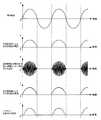
上記充電装置10の回路構成による作用を図2に示す特性図を参照しながら説明する。A positive electrode of the
The effect | action by the circuit structure of the said
充電を開始する前に、充電出力端子29に、例えば、1.0Cが30Aの充電対象の鉛蓄電池12を接続し、接続した鉛蓄電池12の定格電流に合わせて誘導コイル23と受電コイル24との間のギャップを調整する。誘導コイル23と受電コイル24との間のギャップにより受電コイル24に誘起される起電力が調整され、並列共振回路から出力される電流(誘起される起電力に応じて、負荷の大小に無関係に増減する電流)が調整される。例えば、一定のギャップで、且つ絶縁トランス26の一次巻線と二次巻線の巻線比により1.0Cが30Aの鉛蓄電池12へ供給する電流が設定されているとき{例えば、3.0C=90Aに設定されているとき}、充電対象の鉛蓄電池12の1.0Cが30Aより小さい場合、ギャップを広げ、30Aより大きい場合、ギャップを縮める。 Before starting charging, for example, a
そして、給電入力端子20に商用電源11を接続する。
1.充電装置10の給電入力端子20に商用電源11が接続されると、交流電流が半波整流器21へ供給され、半波整流器21で半波整流された直流電流が高周波発生回路22へ供給される。Then, the
1. When the
2.高周波発生回路22は、商用電源11の周波数の半サイクル毎に半サイクルを空けて、半サイクルの波形を包絡線とする所定周波数(例えば、10kHz)の高周波電流を発生し、誘導コイル23へ出力する。 2. The high
3.誘導コイル23により発生する磁束により、受電コイル24には、商用電源11の周波数の半サイクルの波形を包絡線とする前記所定周波数の起電力が誘起され、並列共振回路の出力電流は、誘起された起電力に比例して増減する。このとき、並列共振回路の作用により、負荷の大小に無関係に並列共振回路の出力電流は増減し、負荷が小さくなることにより出力電流が極端に大きくなることが防止され、負荷が変化しても、半波の電流で充電を続行でき、並列共振回路の出力電流のピーク電流が抑えられる。よって鉛蓄電池12に充電する電流を最適な電流とすることが可能となり、目的の電流で充電できる。 3. Due to the magnetic flux generated by the
4.並列共振回路より出力された電流は、絶縁トランス26により鉛蓄電池12へ供給する電流(例えば、3.0C)へ変換される。
5.全波整流器27により所定周波数の電流が全波整流されることにより、全波整流器27の出力電流の波形は、半波整流器21の半波整流後の電圧と略同様の休止する商用周波数の波形を包絡線とする高周波の波形(略商用周波数の半サイクル毎に半サイクルを空けた波形)となり、続けてDCチョーク28により電流が流れ続けようとする作用により、商用周波数の波形を包絡線とする高周波の電流が平滑されて、滑らかな半サイクルの波形となり、充電出力端子29へ出力される。4). The current output from the parallel resonance circuit is converted into a current (for example, 3.0 C) supplied to the
5. The current of a predetermined frequency is full-wave rectified by the full-
6.鉛蓄電池12ヘは、充電出力端子29より略商用電源の周波数の半サイクル毎に滑らかな波形の半波電流が供給される。なお、次の半サイクルでは充電電流はゼロとなる。そして、鉛蓄電池12には所定電流未満では充電は実行されないことから、半波電流の電流値が所定電流以上となると、鉛蓄電池12に充電される。すなわち、ピーク電流が抑えられた商用周波数の半サイクルで充電が実行され、次の半サイクルでは充電が実行されない、半波ではあるが定電流ではない山なりの電流によるパルス充電方式で、鉛蓄電池12が充電される。 6). The lead-
以上のように、本実施の形態によれば、半波整流器21と高周波発生回路22との間に平滑回路が存在しないことにより、高周波発生回路22、誘導コイル23、受電コイル24、共振コンデンサ25、絶縁トランス26、および全波整流器27を介して、鉛蓄電池12へ、商用電源11の周波数の半サイクル毎に半サイクルを空けた波形の電流が供給され、鉛蓄電池12には商用周波数の半サイクルで充電が実行され、鉛蓄電池12に対する充電を、商用周波数の半サイクルの波形による、半波ではあるが定電流ではない山なりの電流によるパルス充電方式とすることができ、よって、簡単な回路構成で、鉛蓄電池12を急速充電でき、さらに鉛蓄電池12の寿命を延長することができる。 As described above, according to the present embodiment, since there is no smoothing circuit between the half-
また本実施の形態によれば、DCチョーク28の作用により鉛蓄電池12に滑らかな半サイクルの波形の半波電流を供給でき、ノイズの発生を回避できる。
また本実施の形態によれば、絶縁トランス26により、充電対象の鉛蓄電池12の定格電流に適応して充電電流(例えば、ピーク電流で90A)を供給することができる。In addition, according to the present embodiment, a smooth half-cycle waveform half-wave current can be supplied to the
In addition, according to the present embodiment, the insulating
また本実施の形態によれば、非接触で絶縁トランス26を使用することで、50Aとか100Aとかの大きな電流でパルスを発生する充電装置10を、簡易な回路構成とすることができ、また絶縁トランス26は、入力が高周波であることから大きさ(サイズ)が小さく安価な高周波トランスを使用でき、さらに半波整流器21と高周波発生回路22との間に平滑回路がなく平滑コンデンサを不要とすることができることにより、充電装置10を、簡易な回路構成で、効率がよく、小さいサイズで、安価に実現することができる。 Further, according to the present embodiment, by using the insulating
また本実施の形態によれば、絶縁トランス26に設定した充電対象の鉛蓄電池12とは定格電流が異なる鉛蓄電池12が充電対象なった場合は、誘導コイル23と受電コイル24との間のギャップを調整することにより、最適な充電電流を供給することができる。すなわち、前記ギャップを調整することにより、鉛蓄電池12の容量(定格)に合わせて、最適なピーク電流および平均電流に調整することができる。 In addition, according to the present embodiment, when a
なお、本実施の形態は、鉛蓄電池12を主な充電対象としているが、パルス充電方式が充電として有効な蓄電池に適用できることはいうまでもない。
[詳細回路]
高周波発生回路22について、具体的な回路構成を図3に示す。図3の高周波発生回路22は、自励式のプッシュプル回路を構成しており、後述するトランジスタ39,40の駆動回路を不要としている。In addition, although this Embodiment makes the
[Detailed circuit]
A specific circuit configuration of the high
高周波発生回路22は、
半波整流器21のプラス出力端子21aに一端が接続され、半波整流器21より直流電流が供給されるDCチョーク31と、
DCチョーク31の他端にセンタータップ23aが接続されたセンタータップ付き一次コイル33、誘導コイル23に接続された二次コイル34、および整流器21のマイナス出力端子21bにセンタータップ35aが接続されたセンタータップ付き三次コイル35からなる絶縁トランス36と、
二次コイル34の両端に並列接続され、誘導コイル23と所定周波数で共振回路を形成する共振コンデンサ37と、
前記センタータップ付き一次コイル33の一端33bと前記整流器21のマイナス出力端子21bとの間に接続された第1トランジスタ39と、
前記センタータップ付き一次コイル33の他端33cと前記整流器21のマイナス出力端子21bとの間に接続された第2トランジスタ40と、
アノードが、前記センタータップ付き一次コイル33の他端33cに接続された、例えば10mAに電流を一定とする第1定電流ダイオード41と、
カソードが、前記第1定電流ダイオード41のカソードおよび前記第1トランジスタ39のゲートに接続され、アノードが、前記整流器21のマイナス出力端子21bに接続された第1ツェナーダイオード43と、
アノードが、前記センタータップ付き一次コイル33の一端33bに接続された、例えば10mAに電流を一定とする第2定電流ダイオード42と、
カソードが、前記第2定電流ダイオード42のカソードおよび前記第2トランジスタ40のゲートに接続され、アノードが、前記半波整流器21のマイナス出力端子21bに接続された第2ツェナーダイオード44と、
アノードが、前記第1定電流ダイオード41のカソードに接続され、カソードが、前記センタータップ付き一次コイル33の他端33cに接続された第1切換えダイオード45と、
アノードが、前記第2定電流ダイオード42のカソードに接続され、カソードが、前記センタータップ付き一次コイル33の一端33bに接続された第2切換えダイオード46と、
第1トランジスタ39のゲートへ電荷を供給する第1駆動回路47と、
第2トランジスタ40のゲートへ電荷を供給する第2駆動回路48と、
第1トランジスタ39のゲートへ急速に電荷を供給する第1進み回路49と、
第2トランジスタ40のゲートへ急速に電荷を供給する第2進み回路50と、
これら部品が配置された空冷用の冷却フィン(図示せず)と
から構成されている。The high
A
A
A resonant capacitor 37 connected in parallel to both ends of the
A
A
A first constant current diode 41 whose anode is connected to the
A first Zener diode 43 having a cathode connected to the cathode of the first constant current diode 41 and the gate of the
A second constant current diode 42 whose anode is connected to one
A
A first switching diode 45 having an anode connected to the cathode of the first constant current diode 41 and a cathode connected to the
A second switching diode 46 having an anode connected to the cathode of the second constant current diode 42 and a cathode connected to one
A first drive circuit 47 for supplying charge to the gate of the
A
A
A
It consists of cooling fins (not shown) for air cooling in which these components are arranged.
前記絶縁トランス36のセンタータップ付き一次コイル33と、二次コイル34と、センタータップ付三次コイル35の巻線比は、センタータップ付き一次コイル33の両端電圧がAC200Vとなる時、二次コイル34の両端電圧が、例えば、AC480V、センタータップ付き三次コイル35の両端電圧が大きく降圧するように、例えば48Vとなるように設定されている。 The winding ratio of the
また前記第1定電流ダイオード41と前記第1ツェナーダイオード43とにより、第1トランジスタ39のゲートに電圧を印加し、第1トランジスタ39をオン(導通)状態にする第1立ち上げ回路51が構成され、また前記第2定電流ダイオード42と前記第2ツェナーダイオード44により、第2トランジスタ40のゲートに電圧を印加し、第2トランジスタ40をオン(導通)状態にする第2立ち上げ回路52が構成されている。 The first constant current diode 41 and the first Zener diode 43 constitute a first start-up
また前記第1駆動回路47は、
前記センタータップ付き三次コイル35の一端35bに、一端が接続された第1乗換え抵抗57と、
アノードが、前記第1乗換え抵抗57の他端に接続され、カソードが、第1定電流ダイオード41のカソードおよび第1トランジスタ39のゲートに接続された第1乗換えダイオード58と
から構成され、
前記第2駆動回路48は、
前記センタータップ付き三次コイル25の他端に、一端が接続された第2乗換え抵抗59と、
アノードが、前記第2乗換え抵抗59の他端に接続され、カソードが、第2定電流ダイオード42のカソードおよび第2トランジスタ40のゲートに接続された第2乗換えダイオード60と
から構成されている。The first drive circuit 47 includes:
A first transfer resistor 57 having one end connected to one
The anode is connected to the other end of the first transfer resistor 57, and the cathode is composed of a first transfer diode 58 connected to the cathode of the first constant current diode 41 and the gate of the
The
A
The anode is connected to the other end of the
また前記第1進み回路49は、
前記センタータップ付き三次コイル35の一端35bに、一端が接続された第1進み抵抗61と、
一端が前記第1進み抵抗61の他端に接続された第1進みコンデンサ62と、
アノードが、前記第1進みコンデンサ62の他端に接続され、カソードが、前記第1定電流ダイオード41のカソードおよび第1トランジスタ39のゲートに接続された第1進みダイオード63と、
前記第1進みダイオード63のアノードと前記整流器21のマイナス出力端子21bとの間に接続された第1抵抗64と、
から構成され、
前記第2進み回路50は、
前記センタータップ付き三次コイル35の他端35cに、一端が接続された第2進み抵抗65と、
一端が前記第2進み抵抗65の他端に接続された第2進みコンデンサ66と、
アノードが、前記第2進みコンデンサ66の他端に接続され、カソードが、前記第2定電流ダイオード42のカソードおよび第2トランジスタ40のゲートに接続された第2進みダイオード67と、
前記第2進みダイオード67のアノードと前記整流器21のマイナス出力端子21bとの間に接続された第2抵抗68と
から構成されている。Further, the
A first advance resistor 61 having one end connected to one
A first lead capacitor 62 having one end connected to the other end of the first lead resistor 61;
A first lead diode 63 having an anode connected to the other end of the first lead capacitor 62 and a cathode connected to the cathode of the first constant current diode 41 and the gate of the
A first resistor 64 connected between the anode of the first lead diode 63 and the
Consisting of
The
A second lead resistor 65 having one end connected to the other end 35c of the tertiary coil 35 with the center tap;
A second lead capacitor 66 having one end connected to the other end of the second lead resistor 65;
A second lead diode 67 having an anode connected to the other end of the second lead capacitor 66 and a cathode connected to the cathode of the second constant current diode 42 and the gate of the
The
また前記誘導コイル23は、磁心を形成するフェライトコア部材に巻かれて給電ユニット69が構成され、また前記受電コイル24は、磁心を形成するフェライトコア部材に巻かれて受電ユニット69が構成されている。 The
給電ユニット69は、図5に示すように、
平板状のフェライトコア部材71a,71c,71dの組み合わせにより構成された側面形状がコ字状の第1フェライト72と、
前記第1フェライト72に対向して配置され、平板状のフェライトコア部材71a,71c,71dの組み合わせにより構成された側面形状がコ字状の第2フェライト73と、
平板状のフェライトコア部材71bにより構成され、前記第1フェライト72の両側の各凸部を形成するフェライト72c,72dの底部にそれぞれ位置するフェライト72a,72bと前記第2フェライト73の両側の各凸部を形成するフェライト73c,73dの底部にそれぞれ位置するフェライト73a,73bとの間をそれぞれ結合する第3フェライト74(74a,74b)と、
前記第1フェライト72の両側の各凸部を形成するフェライト72c,72dに巻かれた前記誘電コイル23aと、
前記誘電コイル23aと直列接続され、前記誘電コイル23aとは逆極性となるように、前記第2フェライト73の両側の各凸部を形成するフェライト73c,73dに巻かれた前記誘導コイル23bと、
第1フェライト72および第2フェライト73を支持するアルミ製の床材75と
から形成されている。誘電コイル23aと誘導コイル23bとにより誘導コイル23が形成されている。As shown in FIG.
A
A
The
The
An
上記給電ユニット69の構成により、誘導コイル23a,23bに給電されると、磁束が発生し、その磁束経路は、図5に示すように、
第1フェライト72の他方側の底部のフェライト72b−第1フェライト72の一方側の底部のフェライト72a−第1フェライト72の一方側の凸部のフェライト72c−第1フェライト72の他方側の凸部のフェライト72d−第1フェライト72の他方側の底部のフェライト72bと、
第1フェライト72の一方側の底部のフェライト72a−第1フェライト72の一方側の凸部のフェライト72c−第2フェライト73の一方側の凸部のフェライト73c−第2フェライト73の一方側の底部のフェライト73a−第3フェライト74a−第1フェライト72の一方側の底部のフェライト72aと、
第2フェライト73の一方側の底部のフェライト73a−第2フェライト73の他方側の底部のフェライト73b−第2フェライト73の他方側の凸部のフェライト73d−第2フェライト73の一方側の凸部のフェライト73c−第2フェライトの一方側の底部のフェライト73aと、
第2フェライト73の他方側の底部のフェライト73b−第2フェライト73の他方側の凸部のフェライト73d−第1フェライト72の他方側の凸部のフェライト72d−第1フェライト72の他方側の底部のフェライト72b−第3フェライト74b−第2フェライト73の他方側の底部のフェライト73bと
の4通りに形成され、これら4通りの磁束経路によって給電ユニット69から受電ユニット70へ飛ぶ磁束を最大とすることができ、電力の伝送効率を向上させることができる。With the configuration of the
Ferrite 73a on the bottom of one side of the second ferrite 73-
また前記受電ユニット69は、図5に示すように、
平板上のフェライトコア部材81a,81c,81dの組み合わせにより構成された側面形状がコ字状の第1フェライト82と、
第1フェライト82に対向して配置され、平板上のフェライトコア部材81a,81c,81dの組み合わせにより構成された側面形状がコ字状の第2フェライト83と、
平板状のフェライトコア部材81bにより構成され、第1フェライト82の両側の各凸部を形成するフェライト82c,82dの底部にそれぞれ位置するフェライト82a,82bと第2フェライト83の両側の各凸部を形成するフェライト83c,83dの底部にそれぞれ位置するフェライト83a,83bをそれぞれ結合する第3フェライト84(84a,84b)と、
第1フェライト82の両側の各凸部を形成するフェライト82c,82dに巻かれた受電コイル24aと、
受電コイル24aと並列接続され、受電コイル24aとは逆極性となるように、第2フェライト83の両側の各凸部を形成するフェライト83c,83dに巻かれた受電コイル24bと、
第1フェライト82および第2フェライト83を支持するアルミ製の床材85と
から形成されている。受電コイル24aと受電コイル24bとにより、受電コイル24が形成されている。In addition, as shown in FIG.
A
A
Each of the convex portions on both sides of the
A
A
An
そして、図5に示すように、受電ユニット70(受電コイル24)は、受電ユニット70の凸部の先端に配置された4つのフェライトコア部材81が、給電ユニット69の4つの凸部の先端に配置されたフェライトコア部材71に対向するように配置される。 As shown in FIG. 5, the power receiving unit 70 (the power receiving coil 24) has four ferrite core members 81 arranged at the tips of the convex portions of the
上記詳細回路の構成による動作を図4を用いて説明する。
1.充電装置10が商用電源11に接続されると、交流電流が半波整流器21へ供給され、半端整流器21で整流された直流電流が高周波発生回路22のDCチョーク31に供給される。この状態では、第1トランジスタ39、第2トランジスタ40ともにオフ(非導通)状態にある。The operation of the detailed circuit configuration will be described with reference to FIG.
1. When charging
2.DCチョーク31に供給された直流電流は、部品の定格が同じでも、第1トランジスタ39、第2トランジスタ40の特性のバラツキなどで電流の流れやすさに差が出る。ここで、センタータップ付き一次コイル33の他端33cから第1定電流ダイオード41を介して第1ツェナーダイオード43に電流が流れて、第1トランジスタ39のゲート電圧が、閾値電圧以上となり、第1トランジスタ39が先にオン(導通)状態となるものとする(図4の第1トランジスタ29のゲートがオンの状態)。 2. The direct current supplied to the
第1トランジスタ39がオン(導通)状態となると、一次コイル33の一端33bから第1トランジスタ39、整流器21のマイナス出力端子21bと電流が流れる。
すると、センタータップ付き一次コイル33の一端33bと第1トランジスタ39のコレクタの接続点の電圧は略0Vとなるため、第2トランジスタ40のゲートの電荷は、第2切換ダイオード46を介して、センタータップ付き一次コイルの一端と第1トランジスタ39のコレクタの接続点へと流れて放電され、第2トランジスタ40は完全にオフ(非導通)状態となり、第2トランジスタ40のゲート電圧が閾値電圧を越えることはない。When the
Then, since the voltage at the connection point between the one
3.さらに、このとき、三次コイル35には、一次コイル33の一端33bから第1トランジスタ39、整流器21のマイナス出力端子21bと流れる電流によって一次コイル33に発生する磁束により起電力が発生し、極性が逆なことから、一次コイル33に流れる電流とは逆方向の誘導電流が流れ、この誘導電流は、三次コイル35の他端35cから第2進み抵抗65、第2進みコンデンサ66、第2抵抗68、三次コイル35のセンタータップ35aと流れ、第2の閉ループが形成されて第2進みコンデンサ66に電荷が蓄えられ、同時に三次コイル35の他端35cから、第2進み抵抗65、第2進みコンデンサ66、第2進みダイオード67、第2切換ダイオード46を介して、センタータップ付き一次コイル33の一端33bと第1トランジスタ39のコレクタの接続点へ流れ、さらに三次コイル35の他端35cから、第2乗換え抵抗59、第2乗換えダイオード60、第2切換ダイオード46を介して、センタータップ付き一次コイル33の一端33bと第1トランジスタ39のコレクタの接続点へ流れ、第2トランジスタ40のゲート電圧が閾値電圧を超えることはない。 3. Further, at this time, an electromotive force is generated in the tertiary coil 35 due to the magnetic flux generated in the
4.次に、センタータップ付き一次コイル33に流れる第1トランジスタ39の電流は、二次コイル34を通じて、共振コンデンサ37および誘導コイル23(23a,23b)に電流を供給し、共振コンデンサ37および誘導コイル23は、所定の周波数で共振を開始し、二次コイル34の両端の電圧は、一定時間の後に逆転するので、これによってセンタータップ付き一次コイル33の他端33cの電圧が一端33bの電圧より、低くなる。 4). Next, the current of the
5.そうすると、第1トランジスタ39のゲートの電荷は、第1切換えダイオード41、一次コイル33の他端33cへと流れ、第1トランジスタ39のゲート電圧が閾値電圧を下回ると、第1トランジスタ39がオフ(非導通)状態となり、同時に、前記第2の閉ループの第2進みコンデンサ66に蓄えられた電荷は、第2進みダイオード67を介して、急激に第2トランジスタ40のゲートへ流れ、同時に、第2乗換え抵抗59、第2乗換えダイオード60を介して、第2トランジスタ40のゲートと流れ、第2トランジスタ40のゲート電圧が、急速に閾値電圧以上となり、第2トランジスタ40がオン(導通)状態となる(図4に示す第2トランジスタ30のゲートがオンの状態)。 5. Then, the charge of the gate of the
第2トランジスタ40がオン(導通)状態となると、一次コイル33の他端33cから第2トランジスタ40、整流器21のマイナス出力端子21bと電流が流れる。
すると、センタータップ付き一次コイル33の他端33Cと第2トランジスタ40のコレクタの接続点の電圧は略0Vとなるため、第1トランジスタ39のゲートの電荷は第1切換ダイオード45を介して、センタータップ付き一次コイル33の他端33Cと第2トランジスタ40のコレクタの接続点へと流れ、放電され、第1トランジスタ39は完全にオフ(非導通)状態となり、第1トランジスタ39のゲート電圧が閾値電圧を越えることはない。When the
Then, since the voltage at the connection point between the other end 33C of the
6.さらに、このとき、三次コイル35には、一次コイル33の他端33cから第2トランジスタ40、整流器21のマイナス出力端子21bと流れる電流によって一次コイル33に発生する磁束により起電力が発生し、極性が逆なことから、一次コイル33に流れる電流とは逆方向の誘導電流が流れ、この誘導電流は、三次コイル35の一端35bから第1進み抵抗61、第1進みコンデンサ62、第1抵抗64、三次コイル35のセンタータップ35aと流れ、第1の閉ループが形成されて第1進みコンデンサ62に電荷が蓄えられ、同時に三次コイル35の一端35bから、第1進み抵抗61、第1進みコンデンサ62、第1進みダイオード63、第1切換ダイオード41を介して、センタータップ付き一次コイル33の他端33Cと第2トランジスタ40のコレクタの接続点へ流れ、さらに三次コイル35の一端35bから、第1乗換え抵抗57、第1乗換えダイオード58、第1切換ダイオード41を介して、センタータップ付き一次コイル33の他端33Cと第1トランジスタ39のコレクタの接続点へ流れ、第1トランジスタ39のゲート電圧が閾値電圧を超えることはない。 6). Further, at this time, an electromotive force is generated in the tertiary coil 35 by the magnetic flux generated in the
7.次に、センタータップ付き一次コイル33に流れる第2トランジスタ40の電流は、二次コイル34を通じて、共振コンデンサ37および誘導コイル23(23a,23b)に電流を供給し、共振コンデンサ37および誘導コイル23は、所定の周波数で共振し、二次コイル34の両端の電圧は、一定時間の後に逆転するので、これによってセンタータップ付き一次コイル33の一端33bの電圧が他端33cの電圧より、低くなる。 7). Next, the current of the
8.そうすると、第2トランジスタ40のゲートの電荷は、第2切換えダイオード46、一次コイル33の一端33bへと流れ、第2トランジスタ40のゲート電圧が閾値電圧を下回ると、第2トランジスタ40がオフ(非導通)状態となると同時に、前記第1の閉ループの第1進みコンデンサ62に蓄えられていた電荷は、第1進みダイオード63を介して、急激に第1トランジスタ39のゲートへ流れ、同時に、第1乗換え抵抗57、第1乗換えダイオード58を介して、第1トランジスタ39のゲートと流れ、第1トランジスタ39のゲート電圧が、急速に閾値電圧以上となり、第1トランジスタ39がオン(導通)状態となる。 8). Then, the charge of the gate of the
以上の動作を繰り返すことにより発振する。
このように、第1トランジスタ39と第2トランジスタ40が交互にオン(導通)状態となり、その毎に、一次コイル33に流れる電流の向きは逆になる。Oscillation occurs by repeating the above operation.
In this way, the
9.これに伴い、二次コイル34に交互に逆向きの電流が流れ、共振コンデンサ37および誘導コイル23(23a,23b)からなる共振回路の周波数が、共振周波数(例えば、12kHz)のときに最も良く電流が良く流れることから、第1トランジスタ39と第2トランジスタ40は、前記共振周波数で交互に180゜ずれてスイッチングされる。すなわち、共振コンデンサ37と誘導コイル23からなる回路の共振周波数で自己発振し、この共振周波数の交流電流が誘導コイル23に供給され、図4に示すように、一次コイル33には、半波整流器21から出力される半波電圧の波形を包絡線とする共振周波数の電圧が発生する。 9. Along with this, reverse current flows alternately through the
このように、電力損失の原因となるAC/DCコンバータを設けることなく、誘導コイル23へ商用電源11から電力を供給でき、電力の伝送効率を向上させることができる。
10.給電ユニット69に対向する受電ユニット70においては、誘導コイル23に発生する磁束により、誘導コイル23の周波数に共振する受電コイル24に大きな起電力が発生する。Thus, power can be supplied from the
10. In the
この起電力により受電コイル24に並列に接続された絶縁トランス26の一次巻線に交流電流が流れ、一次巻線に発生する電圧に対して巻線数の比により絶縁トランス26の二次巻線に降圧された電圧が発生し、増加した交流電流が流れる。この交流電流は全波整流器27へ供給され、この全波整流器27で整流された直流電流は、DCチョーク28を介して鉛蓄電池12へ流れ、鉛蓄電池12が充電される。 This electromotive force causes an alternating current to flow in the primary winding of the insulating
このとき、上述したように、半波整流器21の半波整流後の電圧と略同様の休止する商用周波数の半サイクルの波形となり、一方、鉛蓄電池12には一定電流以上の電流のときしか充電は実行されず、商用周波数の半サイクルで充電されることにより、鉛蓄電池12に対する充電がパルス充電となる。このように、半波ではあるが定電流ではない山なりの電流によるパルス充電方式となることにより、鉛蓄電池12を急速充電でき、さらに鉛蓄電池12の寿命を延長することができる。 At this time, as described above, the half-cycle waveform of the commercial frequency to be paused is substantially the same as the voltage after the half-wave rectification of the half-
このような詳細回路の構成によれば、交流の商用電源11に直接接続しても、第1立ち上げ回路51、第2立ち上げ回路52、第1駆動回路47、第2駆動回路48、第1進み回路49、および第2進み回路50の作用により、第1トランジスタ39または第2トランジスタ40は、二次コイル34に所定周波数で交流電流が流れるように、遅れることなく安定して交互に駆動されるために、前記第1トランジスタ39と前記第2トランジスタ40が同時にオフ(非導通)状態となる可能性が低減され、スイッチング動作の安定性を確保でき、電力の伝送効率を向上させることができる。 According to the configuration of such a detailed circuit, the
10 充電装置
11 商用電源
12 鉛蓄電池
21 半波整流器
22 高周波発生回路
23 誘導コイル
24 受電コイル
25 共振コンデンサ
26 絶縁トランス
27 全波整流器
28 DCチョークDESCRIPTION OF
Claims (4)
Translated fromJapanese前記商用電源から供給される交流電流を半波整流する半波整流器と、
前記半波整流器により半波整流された出力電流を所定周波数の高周波電流へ変換して出力する高周波発生回路と、
前記高周波発生回路より前記高周波電流が供給される誘導コイルと、
前記誘導コイルに対向して配置され、誘導コイルに発生する磁束により起電力が誘起される受電コイルと、
前記受電コイルに並列に接続され、受電コイルとともに前記所定周波数で共振回路を形成する共振コンデンサと、
前記共振回路の出力電流を全波整流し、前記鉛蓄電池へ供給する全波整流器
を備えることを特徴とする鉛蓄電池の充電装置。A charging device for charging a lead-acid battery using a commercial power source,
A half-wave rectifier for half-wave rectifying an alternating current supplied from the commercial power supply;
A high-frequency generating circuit for converting the output current half-wave rectified by the half-wave rectifier into a high-frequency current of a predetermined frequency and outputting it;
An induction coil to which the high-frequency current is supplied from the high-frequency generation circuit;
A power receiving coil disposed opposite to the induction coil and in which an electromotive force is induced by a magnetic flux generated in the induction coil;
A resonance capacitor connected in parallel to the power reception coil and forming a resonance circuit at the predetermined frequency together with the power reception coil;
Full-wave rectifying the output current beforeSymbol co-oscillating circuit, the charging device of a lead-acid battery, characterized in that it comprises a full-wave rectifier supplied to the lead-acid battery.
を特徴とする請求項1に記載の鉛蓄電池の充電装置。The lead-acid battery charging device according to claim 1, wherein the lead-acid battery is charged from the full-wave rectifier via a DC choke.
を特徴とする請求項1または請求項2に記載の鉛蓄電池の充電装置。An insulating transformer is disposed between the resonant circuit and the full-wave rectifier, and a current supplied to the lead storage battery is set according to a winding ratio of a primary winding and a secondary winding of the insulating transformer. The lead-acid battery charging device according to claim 1 or 2.
を特徴とする請求項1〜請求項3のいずれか1項に記載の鉛蓄電池の充電装置。The lead-acid battery charging device according to any one of claims 1 to 3, wherein a current supplied to the lead-acid battery is varied by varying a distance between the induction coil and the power-receiving coil. .
Priority Applications (1)
| Application Number | Priority Date | Filing Date | Title |
|---|---|---|---|
| JP2010006341AJP5454781B2 (en) | 2010-01-15 | 2010-01-15 | Lead-acid battery charger |
Applications Claiming Priority (1)
| Application Number | Priority Date | Filing Date | Title |
|---|---|---|---|
| JP2010006341AJP5454781B2 (en) | 2010-01-15 | 2010-01-15 | Lead-acid battery charger |
Publications (2)
| Publication Number | Publication Date |
|---|---|
| JP2011147278A JP2011147278A (en) | 2011-07-28 |
| JP5454781B2true JP5454781B2 (en) | 2014-03-26 |
Family
ID=44461618
Family Applications (1)
| Application Number | Title | Priority Date | Filing Date |
|---|---|---|---|
| JP2010006341AExpired - Fee RelatedJP5454781B2 (en) | 2010-01-15 | 2010-01-15 | Lead-acid battery charger |
Country Status (1)
| Country | Link |
|---|---|
| JP (1) | JP5454781B2 (en) |
Cited By (2)
| Publication number | Priority date | Publication date | Assignee | Title |
|---|---|---|---|---|
| JP2018519780A (en)* | 2016-02-05 | 2018-07-19 | グァンドン オッポ モバイル テレコミュニケーションズ コーポレーション リミテッド | Adapter and charge control method |
| KR101906977B1 (en)* | 2016-02-05 | 2018-10-11 | 광동 오포 모바일 텔레커뮤니케이션즈 코포레이션 리미티드 | Charge mehtod, adapter and mobile terminal |
Families Citing this family (6)
| Publication number | Priority date | Publication date | Assignee | Title |
|---|---|---|---|---|
| WO2013121535A1 (en)* | 2012-02-15 | 2013-08-22 | パイオニア株式会社 | Non-contact power supply apparatus |
| US9641223B2 (en) | 2012-03-26 | 2017-05-02 | Semiconductor Enegry Laboratory Co., Ltd. | Power receiving device and power feeding system |
| JP6089330B2 (en)* | 2012-08-10 | 2017-03-08 | パナソニックIpマネジメント株式会社 | Small electric device and non-contact power transmission device having the same |
| JP5978184B2 (en)* | 2013-09-04 | 2016-08-24 | 株式会社イージーメジャー | Contactless power supply |
| JP6252051B2 (en)* | 2013-09-06 | 2017-12-27 | 株式会社村田製作所 | Power converter |
| GB2531505A (en)* | 2014-10-09 | 2016-04-27 | Bombardier Transp Gmbh | A method of operating an inductive power transfer system and an inductive power transfer system |
Family Cites Families (8)
| Publication number | Priority date | Publication date | Assignee | Title |
|---|---|---|---|---|
| JPH03107337A (en)* | 1989-09-19 | 1991-05-07 | Ueyama:Kk | Power unit |
| JPH09191580A (en)* | 1996-01-12 | 1997-07-22 | Tdk Corp | Non-contact type charging device |
| JPH10136573A (en)* | 1996-10-28 | 1998-05-22 | Sanyo Electric Co Ltd | Charge system of electric vehicle |
| JPH10136588A (en)* | 1996-10-28 | 1998-05-22 | Sanyo Electric Co Ltd | Charge system of motorized vehicle |
| US6239879B1 (en)* | 1998-07-29 | 2001-05-29 | Hewlett-Packard Company | Non-contacting communication and power interface between a printing engine and peripheral systems attached to replaceable printer component |
| JP2000217279A (en)* | 1999-01-26 | 2000-08-04 | Matsushita Electric Ind Co Ltd | Non-contact power supply |
| JP2002049428A (en)* | 2000-08-04 | 2002-02-15 | Kansai Tlo Kk | Immittance transformer and power unit and non-contact feeder system |
| JP2007012546A (en)* | 2005-07-04 | 2007-01-18 | Gs Yuasa Corporation:Kk | Method of charging lead accumulator and charger for lead accumulator |
- 2010
- 2010-01-15JPJP2010006341Apatent/JP5454781B2/ennot_activeExpired - Fee Related
Cited By (33)
| Publication number | Priority date | Publication date | Assignee | Title |
|---|---|---|---|---|
| JP2018519780A (en)* | 2016-02-05 | 2018-07-19 | グァンドン オッポ モバイル テレコミュニケーションズ コーポレーション リミテッド | Adapter and charge control method |
| KR101906977B1 (en)* | 2016-02-05 | 2018-10-11 | 광동 오포 모바일 텔레커뮤니케이션즈 코포레이션 리미티드 | Charge mehtod, adapter and mobile terminal |
| US10291060B2 (en) | 2016-02-05 | 2019-05-14 | Guangdong Oppo Mobile Telecommunications Corp., Ltd. | Adapter and charging control method |
| US10320225B2 (en) | 2016-02-05 | 2019-06-11 | Guangdong Oppo Mobile Telecommunications Corp., Ltd. | Charging system and charging method for increasing service life of battery of terminal and power adapter thereof |
| US10340727B2 (en) | 2016-02-05 | 2019-07-02 | Guangdong Oppo Mobile Telecommunications Corp., Ltd. | Charging system and charging method, and power adapter |
| US10340718B2 (en) | 2016-02-05 | 2019-07-02 | Guangdong Oppo Mobile Telecommunications Corp., Ltd. | Charging system, charging method, and power adapter |
| US10340717B2 (en) | 2016-02-05 | 2019-07-02 | Guangdong Oppo Mobile Telecommunications Corp., Ltd. | Charging system, charging method, and power adapter |
| US10348119B2 (en) | 2016-02-05 | 2019-07-09 | Guangdong Oppo Mobile Telecommunications Corp., Ltd. | Adapter and method for charging control |
| US10381860B2 (en) | 2016-02-05 | 2019-08-13 | Guangdong Oppo Mobile Telecommunications Corp., Ltd. | Adapter and charging control method |
| US10389164B2 (en) | 2016-02-05 | 2019-08-20 | Guangdong Oppo Mobile Telecommunications Corp., Ltd. | Charging system, protection method for preventing from impact of surge voltage and power adapter |
| US10411494B2 (en) | 2016-02-05 | 2019-09-10 | Guangdong Oppo Mobile Telecommunications Corp., Ltd. | Adapter and method for charging control |
| US10411496B2 (en) | 2016-02-05 | 2019-09-10 | Guangdong Oppo Mobile Telecommunications Corp., Ltd. | Charging system and charging method, and power adapter |
| US10461568B2 (en) | 2016-02-05 | 2019-10-29 | Guangdong Oppo Mobile Telecommunications Corp., Ltd. | Charging system, charging method, and power adapter |
| US10491030B2 (en) | 2016-02-05 | 2019-11-26 | Guangdong Oppo Mobile Telecommunications Corp., Ltd. | Charging system and charging method for terminal and terminal |
| US10541553B2 (en) | 2016-02-05 | 2020-01-21 | Guangdong Oppo Mobile Telecommunications Corp., Ltd. | Adapter and charging control method |
| US10566829B2 (en) | 2016-02-05 | 2020-02-18 | Guangdong Oppo Mobile Telecommunications Corp., Ltd. | Adapter and charging control method |
| US10566828B2 (en) | 2016-02-05 | 2020-02-18 | Guangdong Oppo Mobile Telecommunications Corp., Ltd. | Adapter and charging control method |
| US10566827B2 (en) | 2016-02-05 | 2020-02-18 | Guangdong Oppo Mobile Telecommunications Corp., Ltd. | Adapter and charging control method |
| US10581264B2 (en) | 2016-02-05 | 2020-03-03 | Guangdong Oppo Mobile Telecommunications Corp., Ltd. | Adapter and charging control method |
| US10622829B2 (en) | 2016-02-05 | 2020-04-14 | Guangdong Oppo Mobile Telecommunications Corp., Ltd. | Charging control method and apparatus |
| US10637276B2 (en) | 2016-02-05 | 2020-04-28 | Guangdong Oppo Mobile Telecommunications Corp., Ltd. | Adapter and method for charging control |
| US10644529B2 (en) | 2016-02-05 | 2020-05-05 | Guangdong Oppo Mobile Telecommunications Corp., Ltd. | Adapter and method for charging control |
| US10644530B2 (en) | 2016-02-05 | 2020-05-05 | Guangdong Oppo Mobile Telecommunications Corp., Ltd. | Charging system, charging method, and device |
| US10651677B2 (en) | 2016-02-05 | 2020-05-12 | Guangdong Oppo Mobile Telecommunications Corp., Ltd. | Charging system and charging method, and power adapter and switching-mode power supply |
| US10680460B2 (en) | 2016-02-05 | 2020-06-09 | Guangdong Oppo Mobile Telecommunications Corp., Ltd. | Charging system and charging method and power adapter for charging a rechargeable battery |
| US10714963B2 (en) | 2016-02-05 | 2020-07-14 | Guangdong Oppo Mobile Telecommunications Corp., Ltd. | Charging system, charging method, and device |
| US10727687B2 (en) | 2016-02-05 | 2020-07-28 | Guangdong Oppo Mobile Telecommunications Corp., Ltd. | Charging system and method for terminal, power adapter and charging device |
| US10819134B2 (en) | 2016-02-05 | 2020-10-27 | Guangdong Oppo Mobile Telecommuncations Corp., Ltd. | Adapter and method for charging control |
| US10886772B2 (en) | 2016-02-05 | 2021-01-05 | Guangdong Oppo Mobile Telecommunications Corp., Ltd. | Charging system and charging method for terminal, and power adapter |
| US10910866B2 (en) | 2016-02-05 | 2021-02-02 | Guangdong Oppo Mobile Telecommunications Corp., Ltd. | Charging system and charging method for terminal and power adapter |
| US10985595B2 (en) | 2016-02-05 | 2021-04-20 | Guangdong Oppo Mobile Telecommunications Corp., Ltd. | Adapter and method of controlling charging process |
| US11070076B2 (en) | 2016-02-05 | 2021-07-20 | Guangdong Oppo Mobile Telecommunications Corp., Ltd. | Charging method, charging system, and power adapter |
| US11539230B2 (en) | 2016-02-05 | 2022-12-27 | Guangdong Oppo Mobile Telecommunications Corp., Ltd. | Device charging system, charging method, and power adapter |
Also Published As
| Publication number | Publication date |
|---|---|
| JP2011147278A (en) | 2011-07-28 |
Similar Documents
| Publication | Publication Date | Title |
|---|---|---|
| JP5454781B2 (en) | Lead-acid battery charger | |
| US10696182B2 (en) | Integrated dual-output grid-to-vehicle (G2V) and vehicle-to-grid (V2G) onboard charger for plug-in electric vehicles | |
| KR101628133B1 (en) | A Pulse Width Modulation Resonance Converter and Charger for Vehicle Using the Same | |
| JP4539718B2 (en) | Secondary power receiving circuit for contactless power supply equipment | |
| US8933662B2 (en) | Charging apparatus for lead storage battery | |
| US9431840B2 (en) | Charger and driving method thereof | |
| CN102439819B (en) | Contactless power supply equipment | |
| JP6111139B2 (en) | Bi-directional contactless power feeder | |
| US7388760B2 (en) | Switching power supply circuit | |
| JP5472249B2 (en) | Wireless power supply apparatus and wireless power transmission system | |
| JP2016100989A (en) | Direct current conversion device | |
| Han et al. | A high efficiency LLC resonant converter with wide ranged output voltage using adaptive turn ratio scheme for a Li-ion battery charger | |
| US9570225B2 (en) | Magnetoelectric device capable of storing usable electrical energy | |
| US9705409B2 (en) | Equations for an LLC converter having increased power output capabilities | |
| JP2013158168A (en) | Resonant converter | |
| JP4915438B2 (en) | Wireless power supply apparatus and wireless power transmission system | |
| KR101765319B1 (en) | Hybrid converter and control method thereof | |
| KR20160066754A (en) | Improved ZVS active clamp forward converter | |
| JP5451909B2 (en) | Power supply unit and non-contact power supply equipment including the power supply unit | |
| JP2017147823A (en) | Wireless power reception device and wireless power transmission system | |
| JP3478114B2 (en) | Secondary side power receiving circuit of non-contact power supply equipment | |
| US20240234003A9 (en) | Contactless power feed apparatus and power transmission coil | |
| JPWO2020049853A1 (en) | Contactless power supply system | |
| US10084351B2 (en) | Power feeding device | |
| JP5366090B2 (en) | Contactless power supply equipment |
Legal Events
| Date | Code | Title | Description |
|---|---|---|---|
| A711 | Notification of change in applicant | Free format text:JAPANESE INTERMEDIATE CODE: A711 Effective date:20111004 | |
| A621 | Written request for application examination | Free format text:JAPANESE INTERMEDIATE CODE: A621 Effective date:20120206 | |
| A977 | Report on retrieval | Free format text:JAPANESE INTERMEDIATE CODE: A971007 Effective date:20130809 | |
| A131 | Notification of reasons for refusal | Free format text:JAPANESE INTERMEDIATE CODE: A131 Effective date:20130820 | |
| A521 | Request for written amendment filed | Free format text:JAPANESE INTERMEDIATE CODE: A523 Effective date:20130918 | |
| TRDD | Decision of grant or rejection written | ||
| A01 | Written decision to grant a patent or to grant a registration (utility model) | Free format text:JAPANESE INTERMEDIATE CODE: A01 Effective date:20131126 | |
| A61 | First payment of annual fees (during grant procedure) | Free format text:JAPANESE INTERMEDIATE CODE: A61 Effective date:20131224 | |
| R150 | Certificate of patent or registration of utility model | Ref document number:5454781 Country of ref document:JP Free format text:JAPANESE INTERMEDIATE CODE: R150 Free format text:JAPANESE INTERMEDIATE CODE: R150 | |
| S111 | Request for change of ownership or part of ownership | Free format text:JAPANESE INTERMEDIATE CODE: R313117 | |
| R350 | Written notification of registration of transfer | Free format text:JAPANESE INTERMEDIATE CODE: R350 | |
| R250 | Receipt of annual fees | Free format text:JAPANESE INTERMEDIATE CODE: R250 | |
| R250 | Receipt of annual fees | Free format text:JAPANESE INTERMEDIATE CODE: R250 | |
| R250 | Receipt of annual fees | Free format text:JAPANESE INTERMEDIATE CODE: R250 | |
| R250 | Receipt of annual fees | Free format text:JAPANESE INTERMEDIATE CODE: R250 | |
| R250 | Receipt of annual fees | Free format text:JAPANESE INTERMEDIATE CODE: R250 | |
| R250 | Receipt of annual fees | Free format text:JAPANESE INTERMEDIATE CODE: R250 | |
| LAPS | Cancellation because of no payment of annual fees |