JP5450329B2 - DC power supply system - Google Patents
DC power supply systemDownload PDFInfo
- Publication number
- JP5450329B2 JP5450329B2JP2010207253AJP2010207253AJP5450329B2JP 5450329 B2JP5450329 B2JP 5450329B2JP 2010207253 AJP2010207253 AJP 2010207253AJP 2010207253 AJP2010207253 AJP 2010207253AJP 5450329 B2JP5450329 B2JP 5450329B2
- Authority
- JP
- Japan
- Prior art keywords
- converter
- voltage
- secondary battery
- power supply
- circuit
- Prior art date
- Legal status (The legal status is an assumption and is not a legal conclusion. Google has not performed a legal analysis and makes no representation as to the accuracy of the status listed.)
- Expired - Fee Related
Links
Images


Classifications
- H—ELECTRICITY
- H02—GENERATION; CONVERSION OR DISTRIBUTION OF ELECTRIC POWER
- H02J—CIRCUIT ARRANGEMENTS OR SYSTEMS FOR SUPPLYING OR DISTRIBUTING ELECTRIC POWER; SYSTEMS FOR STORING ELECTRIC ENERGY
- H02J9/00—Circuit arrangements for emergency or stand-by power supply, e.g. for emergency lighting
- H—ELECTRICITY
- H01—ELECTRIC ELEMENTS
- H01M—PROCESSES OR MEANS, e.g. BATTERIES, FOR THE DIRECT CONVERSION OF CHEMICAL ENERGY INTO ELECTRICAL ENERGY
- H01M10/00—Secondary cells; Manufacture thereof
- H01M10/42—Methods or arrangements for servicing or maintenance of secondary cells or secondary half-cells
- H01M10/44—Methods for charging or discharging
- H—ELECTRICITY
- H02—GENERATION; CONVERSION OR DISTRIBUTION OF ELECTRIC POWER
- H02J—CIRCUIT ARRANGEMENTS OR SYSTEMS FOR SUPPLYING OR DISTRIBUTING ELECTRIC POWER; SYSTEMS FOR STORING ELECTRIC ENERGY
- H02J7/00—Circuit arrangements for charging or depolarising batteries or for supplying loads from batteries
- H02J7/34—Parallel operation in networks using both storage and other DC sources, e.g. providing buffering
- Y—GENERAL TAGGING OF NEW TECHNOLOGICAL DEVELOPMENTS; GENERAL TAGGING OF CROSS-SECTIONAL TECHNOLOGIES SPANNING OVER SEVERAL SECTIONS OF THE IPC; TECHNICAL SUBJECTS COVERED BY FORMER USPC CROSS-REFERENCE ART COLLECTIONS [XRACs] AND DIGESTS
- Y02—TECHNOLOGIES OR APPLICATIONS FOR MITIGATION OR ADAPTATION AGAINST CLIMATE CHANGE
- Y02E—REDUCTION OF GREENHOUSE GAS [GHG] EMISSIONS, RELATED TO ENERGY GENERATION, TRANSMISSION OR DISTRIBUTION
- Y02E60/00—Enabling technologies; Technologies with a potential or indirect contribution to GHG emissions mitigation
- Y02E60/10—Energy storage using batteries
Landscapes
- Engineering & Computer Science (AREA)
- Power Engineering (AREA)
- Manufacturing & Machinery (AREA)
- Chemical & Material Sciences (AREA)
- Chemical Kinetics & Catalysis (AREA)
- Electrochemistry (AREA)
- General Chemical & Material Sciences (AREA)
- Business, Economics & Management (AREA)
- Emergency Management (AREA)
- Charge And Discharge Circuits For Batteries Or The Like (AREA)
- Dc-Dc Converters (AREA)
- Secondary Cells (AREA)
Description
Translated fromJapanese本発明は、二次電池でバックアップされた直流電源システムに関する。 The present invention relates to a DC power supply system backed up by a secondary battery.
近年、太陽光発電や家庭用燃料電池などを用いた直流電源システムが普及しつつある。ところで、太陽電池は、気象条件や温度などによって発電量が変化するため、その出力電圧が安定せず、一般的に二次電池によってバックアップされている(例えば、特許文献1参照)。 In recent years, DC power supply systems using photovoltaic power generation, household fuel cells, and the like are becoming popular. By the way, since the amount of power generation of a solar cell varies depending on weather conditions, temperature, and the like, its output voltage is not stable and is generally backed up by a secondary battery (see, for example, Patent Document 1).
直流電源システムは、二次電池充電用DC/DCコンバータ及び二次電池放電用DC/DCコンバータの並列回路に二次電池が直列接続された回路が、太陽電池などの直流電源と並列に接続されている。通常、二次電池として、その電圧が直流電源の定電圧よりも低いものが使用される。そして、直流電源の電圧が二次電池の電圧よりも高いときは、充電用DC/DCコンバータを介して二次電池に充電用電流が流れ、二次電池が充電される。一方、直流電源の電圧が二次電池の電圧よりも低いときは、放電用DC/DCコンバータを介して二次電池から放電電流が流れ、二次電池から電力が供給される。 In a DC power supply system, a circuit in which a secondary battery is connected in series to a parallel circuit of a DC / DC converter for charging a secondary battery and a DC / DC converter for discharging a secondary battery is connected in parallel with a DC power supply such as a solar battery. ing. Usually, a secondary battery whose voltage is lower than the constant voltage of the DC power supply is used. When the voltage of the DC power supply is higher than the voltage of the secondary battery, a charging current flows through the secondary battery via the charging DC / DC converter, and the secondary battery is charged. On the other hand, when the voltage of the DC power supply is lower than the voltage of the secondary battery, a discharge current flows from the secondary battery via the discharge DC / DC converter, and power is supplied from the secondary battery.
太陽光発電の場合、負荷により電力が消費されていないときでも太陽電池は発電を続けるため、その間を利用して発電された電力が二次電池に充電される。ところが、例えば日照条件が良すぎて太陽電池自体の温度が高くなりすぎると、かえって太陽電池の出力電圧が低下する。特許文献1には、直流電源の電圧が二次電池の電圧よりも低いときに、二次電池に充電することに関して直接の記載はないが、例えば昇圧可能なDC/DCコンバータを用いることにより、二次電池に充電することは可能である。しかしながら、太陽電池の出力電圧を二次電池の電圧以上に昇圧させて充電する場合、DC/DCコンバータの二次側に流れる電流は、DC/DCコンバータの一次側に流れる電流に変換効率及び昇圧率の逆数を掛けた値になり、電流値がかなり小さくなる。すなわち、充電効率が低下し、エネルギーロスが大きくなる。 In the case of solar power generation, the solar battery continues to generate power even when power is not consumed by the load, and thus the secondary battery is charged with the power generated using that power. However, for example, if the sunshine conditions are too good and the temperature of the solar cell itself becomes too high, the output voltage of the solar cell is lowered. In
本発明は、上記従来例の問題を解決するためになされたものであり、高い充電効率を実現しつつ、直流電源の電圧が二次電池の電圧よりも低いときでも二次電池に充電が可能な直流電源システムを提供することを目的とする。 The present invention has been made to solve the above-described problems of the conventional example, and can charge the secondary battery even when the voltage of the DC power supply is lower than the voltage of the secondary battery while realizing high charging efficiency. An object is to provide a direct current power supply system.
上記目的を達成するために、本発明の一態様に係る直流電源システムは、直流電源とバックアップ用二次電池を備え、前記直流電源の電圧が前記二次電池の電圧よりも低いときに、前記二次電池への入力電圧が前記二次電池の電圧よりも高くなるように、前記二次電池の電力を用いて前記直流電源の電圧をかさ上げし、前記二次電池を充電することを特徴とする。 In order to achieve the above object, a DC power supply system according to an aspect of the present invention includes a DC power supply and a backup secondary battery, and when the voltage of the DC power supply is lower than the voltage of the secondary battery, The secondary battery is charged by raising the voltage of the DC power supply using the power of the secondary battery so that the input voltage to the secondary battery is higher than the voltage of the secondary battery. And
本発明の他の一態様に係る直流電源システムは、直流電源と、前記直流電源と並列に接続され、バックアップ用二次電池を含むバックアップ電源回路を備え、前記バックアップ電源回路は、前記直流電源の電圧が前記二次電池の電圧よりも高いときに、前記二次電池を充電するための第1充電用DC/DCコンバータと、前記直流電源の電圧が前記二次電池の電圧よりも高いときに、前記二次電池に充電された電力を放電するための第1放電用DC/DCコンバータと、前記直流電源の電圧が前記二次電池の電圧よりも低いときに、前記二次電池の電力を用いて前記直流電源の電圧をかさ上げし、前記二次電池を充電するための第2充電用DC/DCコンバータと、前記直流電源の電圧が前記二次電池の電圧よりも低いときに、前記二次電池に充電された電力を放電するための第2放電用DC/DCコンバータと、前記第1充電用DC/DCコンバータ、前記第1放電用DC/DCコンバータ、前記第2充電用DC/DCコンバータ及び前記第2放電用DC/DCコンバータを制御するための制御回路を備えたことを特徴とする。 A DC power supply system according to another aspect of the present invention includes a DC power supply and a backup power supply circuit connected in parallel with the DC power supply and including a backup secondary battery, and the backup power supply circuit includes the DC power supply. When the voltage is higher than the voltage of the secondary battery, the first charging DC / DC converter for charging the secondary battery and the voltage of the DC power supply is higher than the voltage of the secondary battery A first discharge DC / DC converter for discharging the power charged in the secondary battery, and when the voltage of the DC power source is lower than the voltage of the secondary battery, A second charging DC / DC converter for raising the voltage of the DC power source and charging the secondary battery, and when the voltage of the DC power source is lower than the voltage of the secondary battery, Secondary battery A second discharging DC / DC converter for discharging the charged electric power; the first charging DC / DC converter; the first discharging DC / DC converter; the second charging DC / DC converter; A control circuit for controlling the second discharge DC / DC converter is provided.
上記構成において、前記第1充電用DC/DCコンバータと前記第2放電用DC/DCコンバータは同一の第1DC/DCコンバータであり、前記第2充電用DC/DCコンバータと前記第1放電用DC/DCコンバータは前記第1DC/DCコンバータとは異なる同一の第2DC/DCコンバータであることが好ましい。 In the above configuration, the first charging DC / DC converter and the second discharging DC / DC converter are the same first DC / DC converter, and the second charging DC / DC converter and the first discharging DC are the same. The / DC converter is preferably the same second DC / DC converter different from the first DC / DC converter.
また、前記第2DC/DCコンバータは、その入力端子が前記二次電池の両端子に並列接続され、その出力端子が前記直流電源の高圧側端子と前記二次電池の高圧側端子の間に直列接続されていることが好ましい。 The second DC / DC converter has an input terminal connected in parallel to both terminals of the secondary battery, and an output terminal connected in series between the high-voltage side terminal of the DC power supply and the high-voltage side terminal of the secondary battery. It is preferable that they are connected.
また、前記第1DC/DCコンバータは、その入力端子が前記第2DC/DCコンバータの出力端子に接続され、その出力端子が前記二次電池の両端子に接続されていることが好ましい。 The first DC / DC converter preferably has an input terminal connected to an output terminal of the second DC / DC converter and an output terminal connected to both terminals of the secondary battery.
また、前記第1DC/DCコンバータの入力側回路及び前記第2DC/DCコンバータの出力側回路として、GaN/AlGaNを用いた横型トランジスタ構造を有する双方向スイッチ素子を用いたことが好ましい。 Further, it is preferable that a bidirectional switch element having a lateral transistor structure using GaN / AlGaN is used as an input side circuit of the first DC / DC converter and an output side circuit of the second DC / DC converter.
本発明によれば、直流電源の電圧が二次電池の電圧よりも低いときであっても、例えば負荷による電力消費量が少ない場合に、二次電池の電力を用いて直流電源の電圧をかさ上げし、二次電池を充電することができる。それによって、太陽光発電など直流電源によって発電された電力を有効に蓄電して使用することができる。また、昇圧用DC/DCコンバータを用いて直流電源の電圧を直接昇圧しているわけではないので、直流電源から引き込まれた電流を直接充電電流とすることができ、高い充電効率を実現することができる。 According to the present invention, even when the voltage of the DC power supply is lower than the voltage of the secondary battery, for example, when the power consumption by the load is small, the voltage of the DC power supply is increased using the power of the secondary battery. And recharge the secondary battery. Thereby, the electric power generated by the DC power source such as solar power generation can be effectively stored and used. In addition, since the voltage of the DC power supply is not directly boosted using the boosting DC / DC converter, the current drawn from the DC power supply can be directly used as the charging current, and high charging efficiency can be realized. Can do.
本発明の一実施形態に係る直流電源システムについて説明する。この直流電源システム1は、太陽電池や家庭用燃料電池などの直流電源2と、直流電源2と並列に接続され、バックアップ用二次電池3を含むバックアップ電源回路4を備えている。 A DC power supply system according to an embodiment of the present invention will be described. The DC
バックアップ電源回路4は、並列接続された第1DC/DCコンバータ5及び第2DC/DCコンバータ6と、この並列回路に直列接続された二次電池3と、第1DC/DCコンバータ5及び第2DC/DCコンバータ6を制御する制御回路7を備えている。また、バックアップ電源回路4は、直流電源2の電圧V1を検出する第1電圧検出部8と、二次電池3の電圧V2を検出する第2電圧検出部10を備えている。さらに、必要に応じて、バックアップ電源回路4は、負荷20に流れる電流I1を検出する第1電流検出部9と、バックアップ電源回路4に流れる充電電流又は放電電流I2を検出する第2電流検出部11を備えていてもよい。 The backup
第2DC/DCコンバータ6の入力端子は二次電池3の両端子に並列接続され、その出力端子は直流電源2の高圧側端子と二次電池3の高圧側端子の間に直列接続されている。また、第1DC/DCコンバータ5の入力端子は第2DC/DCコンバータ6の出力端子に接続され、その出力端子は二次電池3の両端子に接続されている。 The input terminal of the second DC /
第1DC/DCコンバータ5及び第2DC/DCコンバータ6は、それぞれ直流電源2の電圧V1と二次電池3の電圧V2の大小に応じて、放電用DC/DCコンバータとして機能する場合と、充電用DC/DCコンバータとして機能する場合がある。具体的には、直流電源2の電圧V1が二次電池3の電圧V2よりも高いときは(V1>V2)、第1DC/DCコンバータ5は、二次電池3を充電するための第1充電用DC/DCコンバータとして機能する。直流電源2の電圧V1が二次電池3の電圧V2よりも高いときは(V1>V2)、第2DC/DCコンバータ6は、二次電池3に充電された電力を放電するための第1放電用DC/DCコンバータとして機能する。一方、直流電源2の電圧V1が二次電池3の電圧V2よりも低いときは(V2>V1)、第2DC/DCコンバータ6は、二次電池3を充電するための第2充電用DC/DCコンバータとして機能する。また、直流電源2の電圧V1が二次電池3の電圧V2よりも低いときは(V2>V1)、第1DC/DCコンバータ5は、二次電池3に充電された電力を放電するための第2放電用DC/DCコンバータとして機能する。 The first DC /
第1DC/DCコンバータ5は、トランス51と、入力側(1次側)回路52と、出力側(2次側)回路53などで構成されている。また、第2DC/DCコンバータ6は、トランス61と、入力側(1次側)回路62と、出力側(2次側)回路63などで構成されている。これら第1DC/DCコンバータ5及び第2DC/DCコンバータ6の具体的な回路構成を図6に示す。なお、回路構成の説明は後述する。 The first DC /
制御回路7は、第1電圧検出部8により検出された直流電源2の電圧V1と第2電圧検出部10により検出された二次電池3の電圧V2を比較し、比較結果に応じて、第1DC/DCコンバータ5及び第2DC/DCコンバータ6の入力側回路52,62を制御する。以下に、直流電源2の電圧V1が二次電池3の電圧V2よりも高い場合(V1>V2)と、直流電源2の電圧V1が二次電池3の電圧V2よりも低い場合(V2>V1)に分けて、具体的な動作を説明する。なお、便宜上、二次電池3の電圧を380Vに固定し、電流値はあくまで仮定のものである。 The
(具体的動作例1)
直流電源2の電圧V1が二次電池3の電圧V2よりも高い場合(V1>V2)で、かつ、二次電池3に充電する場合について、図2を参照して説明する。この場合は、例えば負荷20による消費電力が少なく、直流電源2により発電された電力に余裕がある場合などが該当する。第1DC/DCコンバータ5は、第1充電用DC/DCコンバータとして機能する。(Specific operation example 1)
A case where the voltage V1 of the
図2に示すように、直流電源2の電圧V1を400V、二次電池3の電圧V2を380Vと仮定する。制御回路7は、直流電源2の電圧V1と二次電池3の電圧V2の比較結果に応じて、第1DC/DCコンバータ5の入力側(1次側)回路52を駆動させ、直流電源2からこのバックアップ電源回路4に電流を引き込む。 As shown in FIG. 2, it is assumed that the voltage V1 of the
直流電源2からこのバックアップ電源回路4に2Aの電流が引き込まれたと仮定する。第1DC/DCコンバータ5の入力側の電位差は20Vであり、入力側(1次側)の回路52に2Aの電流が流れるので、入力電力は20V×2A=40Wとなる。第1DC/DCコンバータ5の効率を90%と仮定すると、第1DC/DCコンバータ5の出力側(回路53)への出力電力は40W×0.9=36Wとなる。第1DC/DCコンバータ5は、その2次側に二次電池3を充電するために380Vの電圧が発生するように、昇圧比が設定されている。第1DC/DCコンバータ5の出力側回路53には、36W÷380V=0.095Aの電流が流れる。 It is assumed that a current of 2 A is drawn from the
第1DC/DCコンバータ5の入力側回路52に流れる2Aの電流はそのまま2次電池3を介してグランドに流れるので、二次電池3には入力側の2Aと出力側の0.095Aを合わせた2.095Aの電流が流れる。直流電源2からは、400V×2A=800Wの電力が出力され、2次電池3には、380V×2.095A=796Wの電力が充電される。すなわち、この直流電源システム全体の充電効率は、796W÷800W=0.995となり、非常に効率の高い充電回路が得られる。なお、この間、第2DC/DCコンバータ6は機能していない。また、第2電圧検出部10により充電電流I2を検出し、第1DC/DCコンバータ5の出力側回路53に流れる電流を制御することにより、充電電流を定電流制御することができる。 Since the 2 A current flowing in the
(具体的動作例2)
直流電源2の電圧V1が二次電池3の電圧V2よりも高い場合(V1>V2)で、かつ、二次電池3から放電する場合について、図3を参照して説明する。この場合は、例えば太陽電池などの直流電源2の出力電力が低下した場合や、負荷20による消費電力が大きく、直流電源2だけでは十分な電力がまかなえない場合などが該当する。第2DC/DCコンバータ6は、放電用第1DC/DCコンバータとして機能する。(Specific operation example 2)
A case where the voltage V1 of the
制御回路7は、直流電源2の電圧V1と二次電池3の電圧V2の比較結果に応じて、第2DC/DCコンバータ6の入力側(1次側)回路62を駆動させ、第2DC/DCコンバータ6の入力側回路62に、例えば0.1Aの電流を流す。第2DC/DCコンバータ6は、二次電池3の電圧V2(380V)を直流電源2の電圧V1(400V)以上にかさ上げするための電圧を発生させる。 The
第2DC/DCコンバータ6の入力側回路に0.1Aの電流が流れると、第2DC/DCコンバータ6への入力電力は380V×0.1A=38Wとなる。第2DC/DCコンバータ6の効率を90%と仮定すると、第2DC/DCコンバータ6の出力側への出力電力は38W×0.9=34.2Wとなる。第2DC/DCコンバータ6は、その2次側に直流電源2と二次電池3の電圧差を補完する電圧20Vが発生するように、降圧比が設定されている。第2DC/DCコンバータ6の出力側回路63には、34.2W÷20V=1.71Aの電流が流れる。 When a current of 0.1 A flows through the input side circuit of the second DC /
このDCコンバータ6の出力側回路63に流れる電流は二次電池3にも流れるので、二次電池3には、入力側回路62に流れる電流と出力側回路63に流れる電流を合わせた0.1A+1.71A=1.81Aの電流が流れる。二次電池3からは、380V×1.81A=687.8Wの電力が放電される。一方、二次電池3から負荷20に供給される電力は、400V×1.71A=684Wとなる。この直流電源システム全体の放電効率は、684W÷687.8W=0.994となり、非常に効率の高い放電回路が得られる。なお、この間、第1DC/DCコンバータ5は機能していない。 Since the current flowing through the
(具体的動作例3)
直流電源2の電圧V1が二次電池3の電圧V2よりも低い場合(V2>V1)で、かつ、二次電池3に充電する場合について、図4を参照して説明する。この場合は、例えば、負荷20による消費電力が少なく、かつ、太陽電池などの直流電源2の出力電圧が低下した場合などが該当する。第2DC/DCコンバータ6は、充電用第2DC/DCコンバータとして機能する。(Specific operation example 3)
A case where the voltage V1 of the
制御回路7は、直流電源2の電圧V1と二次電池3の電圧V2の比較結果に応じて、第2DC/DCコンバータ6の入力側(1次側)回路62を駆動させ、第2DC/DCコンバータ6の入力側回路62に、例えば0.1Aの電流を流す。第2DC/DCコンバータ6は、直流電源2の電圧V1(360V)を二次電池3の電圧V2(380V)以上にかさ上げするための電圧を発生させる。図3に示す場合と比較して、第2DC/DCコンバータ6の出力側(2次側)回路63に発生される電圧の極性は逆向きとなる。 The
上記の場合と同様に、第2DC/DCコンバータ6の入力側回路62に0.1Aの電流が流れると、第2DC/DCコンバータ6への入力電力は380V×0.1A=38Wとなる。第2DC/DCコンバータ6の効率を90%と仮定すると、第2DC/DCコンバータ6の出力側の出力電力は38W×0.9=34.2Wとなる。第2DC/DCコンバータ6の2次側に直流電源2と二次電池3の電圧差20Vを補完する電圧が発生するように、昇圧比が設定されている。第2DC/DCコンバータ6の出力側回路63には、34.2W÷20V=1.71Aの電流が流れる。但し、電流の流れる方向は逆である。 Similarly to the above case, when a current of 0.1 A flows through the
この第2DC/DCコンバータ6の出力側回路63に流れる電流は、直流電源2からの電力を二次電池3の充電用にバックアップ電源回路4に引き込む。実際に二次電池3に対して充電電流として流れるのは、第2DC/DCコンバータ6の出力側回路63に流れる電流から入力側回路62に流れる電流を差し引いた1.71A−0.1A=1.61Aとなる。 The current flowing through the
直流電源2からは、360V×1.71A=616Wの電力が出力され、2次電池3には、380V×1.61A=612Wの電力が充電される。すなわち、この直流電源システム全体の充電効率は、612W÷616W=0.994となり、非常に効率の高い充電回路が得られる。なお、この間、第1DC/DCコンバータ5は機能していない。また、第2電圧検出部10により充電電流I2を検出し、第2DC/DCコンバータ6の入力側回路62に流れる電流を制御することにより、充電電流を定電流制御することができる。 The
(具体的動作例4)
直流電源2の電圧V1が二次電池3の電圧V2よりも低い場合(V2>V1)で、かつ、二次電池3から放電する場合について、図5を参照して説明する。この場合は、例えば、直流電源2の電圧が低い状態にもかかわらず、負荷20が駆動され続けている場合などが考えられる。この二次電池3は、あくまでも直流電源2をアシストするものでありバックアップ電源回路4は、二次電池3の電圧を直流電源2の電圧に落として出力する。第1DC/DCコンバータ5は、放電用第2DC/DCコンバータとして機能する。(Specific operation example 4)
A case where the voltage V1 of the
制御回路7は、第1電流検出部9により検出された負荷電流I1の値に基づいて、第1DC/DCコンバータ5の入力側(1次側)回路52を導通させ、第1DC/DCコンバータ5の入力側回路に、例えば2Aの電流を流す。第1DC/DCコンバータ5の入力側は、二次電池3の電圧V2(380V)を直流電源2の電圧V1(360V)に降圧させる。同時に、第1DC/DCコンバータ5の出力側には、二次電池3を充電するために380Vの電圧が発生する。 The
第1DC/DCコンバータ5の入力側回路に2Aの電流が流れると、第1DC/DCコンバータ5への入力電力は(380V−360V)×2A=40Wとなる。第1DC/DCコンバータ5の効率を90%と仮定すると、第1DC/DCコンバータ5の出力側の出力電力は40W×0.9=36Wとなる。第1DC/DCコンバータ5の出力側回路53には、36W÷380V=0.095Aの充電電流が流れる。 When a current of 2A flows through the input side circuit of the first DC /
この充電電流は二次電池3に還流されるので、二次電池3からは、上記2Aから充電電流0.095Aを差し引いた1.905Aの電流が流れ、二次電池3からは、380V×1.905A=724Wの電力が放電される。一方、二次電池3から負荷に供給される電力は、360V×2A=720Wとなる。この直流電源システム全体の放電効率は、720W÷724W=0.994となり、非常に効率の高い放電回路が得られる。なお、この間、第2DC/DCコンバータ6は機能していない。また、第1DC/DCコンバータ5の出力側回路53の電流(充電電流)の値を制御することにより、二次電池3から負荷20に流れる放電電流を定電流制御することができる。 Since this charging current is returned to the
上記のように、第1DC/DCコンバータ5及び第2DC/DCコンバータ6は、直流電源2の電圧と二次電池3の電圧の大小に応じて、それぞれ放電用DC/DCコンバータ又は充電用DC/DCコンバータとして機能する。第1DC/DCコンバータ5は、第1充電用DC/DCコンバータとして機能する場合と、第2放電用DC/DCコンバータとして機能する場合とで、入力側に流れる電流の向きが反転し、入力端子の電圧も極性が反転する。同様に、第2DC/DCコンバータ6は、第2充電用DC/DCコンバータとして機能する場合と、第1放電用DC/DCコンバータとして機能する場合とで、出力側に流れる電流の向きが反転し、出力端子の電圧も極性が反転する。そのため、図6に示すように、第1DC/DCコンバータ5の入力側回路52及び第2DC/DCコンバータ6の出力側回路63を構成するスイッチ素子として、双方向スイッチ素子を用いている。 As described above, the first DC /
図6に示すように、第1DC/DCコンバータ5の入力側回路52は、直列接続された2つの双方向スイッチQ1及びQ2を有している。双方向スイッチQ2は、トランス51の1次側巻き線に並列に接続されている。双方向スイッチQ1及びQ2を相互に所定の周波数でオン及びオフさせることにより、トランス51の1次側巻き線にパルス電流が流れ、それによって2次側巻き線に起電力が発生する。入力側回路52には双方向に電流が流れるので、電流の向きに応じて出力側回路53に入力される電圧の極性が反転する。そのため、出力側回路53は、二次電池3を充電するために、トランス51の2次側巻き線に発生された起電力を常に同方向に流すように、ダイオードで構成されている。 As shown in FIG. 6, the
第2DC/DCコンバータ6の入力側回路62は、直列接続された2つのスイッチQ3及びQ4を有している。スイッチQ4は、トランス61の1次側巻き線に並列に接続されている。スイッチQ3及びQ4を相互に所定の周波数でオン及びオフさせることにより、トランス61の1次側巻き線にパルス電流が流れ、それによって2次側巻き線に起電力が発生する。なお、入力側回路62には常に同じ向きに電流が流れるので、出力側回路63に入力される電圧の極性は一定である。ところが、上記のように、第2DC/DCコンバータ6が放電用DC/DCコンバータとして機能する場合と、充電用DC/DCコンバータとして機能する場合とでは、電流の向きが反転する。そのため、出力側回路63は、トランス61の2次巻き線に接続された2つの双方向スイッチQ5及びQ6で構成されている。そして、双方向スイッチQ5がオンの時双方向スイッチQ6をオフし、双方向スイッチQ6がオンの時双方向スイッチQ5をオフすることにより、出力側回路63に流れる電流の向きを反転させる。なお、入力側回路62には常に同じ向きに電流が流れるので、スイッチQ3及びQ4は双方向スイッチである必要はなく、MOSFETなどであってもよい。 The
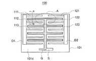
双方向スイッチの具体例として、GaN/AlGaNを用いた横型トランジスタ構造を有する双方向スイッチ素子100の詳細について説明する。図7は双方向スイッチ素子100の構成を示す平面図であり、図8は範囲Aの拡大図、図9はB−B断面図である。なお、この双方向スイッチ素子100は、2つの電極D1及びD2間にゲートGが1つだけ設けられているものはシングルゲート型と呼ばれている。 As a specific example of the bidirectional switch, details of the
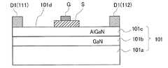
図9に示すように、双方向スイッチ素子100の基板101は、導体層101aと、導体層101aの上に積層されたGaN層2b及びAlGaN層010cで構成されている。この実施形態では、チャネル層としてAlGaN/GaNヘテロ界面に生じる2次元電子ガス層を利用している。図7に示すように、基板101の表面101dには、直流電源2及び負荷3に対してそれぞれ直列に接続された第1電極D1及び第2電極D2と、第1電極D1の電位及び第2電極D2の電位に対して中間電位となる中間電位部Sが形成されている。さらに、中間電位部Sの上には、制御電極(ゲート)Gが積層形成されている。制御電極Gとして、例えばショットキ電極を用いる。第1電極D1及び第2電極D2は、それぞれ互いに平行に配列された複数の電極部111,112,113・・・及び121,122,123・・・を有する櫛歯状であり、櫛歯状に配列された電極部同士が互いに対向するように配置されている。中間電位部S及び制御電極Gは、櫛歯状に配列された電極部111,112,113・・・及び121,122,123・・・の間にそれぞれ配置されており、電極部の間に形成される空間の平面形状に相似した形状(略魚背骨状)を有している。 As shown in FIG. 9, the
次に、双方向スイッチ素子100を構成する横型のトランジスタ構造について説明する。図8に示すように、第1電極D1の電極部111と第2電極D2の電極部121は、それらの幅方向における中心線が同一線上に位置するように配列されている。また、中間電位部S及び制御電極Gは、それぞれ第1電極D1の電極部111及び第2電極D2の電極部121の配列に対して平行に設けられている。上記幅方向における第1電極D1の電極部111と第2電極D2の電極部121と中間電位部S及び制御電極Gの距離は、所定の耐電圧を維持しうる距離に設定されている。上記幅方向に直交する方向、すなわち第1電極D1の電極部111と第2電極D2の電極部121の長手方向においても同様である。また、これらの関係は、その他の電極部112及び122,113及び123・・・についても同様である。すなわち、中間電位部S及び制御電極Gは、第1電極D1及び第2電極D2に対して所定の耐電圧を維持しうる位置に配置されている。 Next, a lateral transistor structure constituting the
そのため、第1電極D1が高電位側、第2電極D2が低電位側である場合、双方向スイッチ素子100がオフのとき、少なくとも第1電極D1と、制御電極G及び中間電位部Sの間で、電流は確実に遮断される(制御電極(ゲート)Gの直下で電流が阻止される)。一方、双方向スイッチ素子100がオンのとき、すなわち制御電極Gに所定の閾値以上の電圧の信号が印加されたときは、図中矢印で示すように、第1電極D1(電極部111・・・)、中間電位部S、第2電極D2(電極部121・・・)の経路で電流が流れる。逆の場合も同様である。その結果、制御電極Gに印加する信号の閾値電圧を必要最低限のレベルまで低下させても、双方向スイッチ素子100を確実にオン/オフさせることができ、低オン抵抗を実現することができる。また、第1電極D1の電極部111,112,113・・・及び第2電極D2の電極部121,122,123・・・を櫛歯状に配列することができ、双方向スイッチ素子100のチップサイズを大きくすることなく、大電流を取り出すことができる。 Therefore, when the first electrode D1 is on the high potential side and the second electrode D2 is on the low potential side, when the
図10及び11は、GaN/AlGaNを用いた横型トランジスタ構造を有する他の双方向スイッチ素子300の構成を示す。図10は双方向スイッチ素子300の構成を示す平面図であり、図11はC−C断面図である。なお、この双方向スイッチ素子300は、2つの電極D1及びD2間に2つのゲートG1及びG2が設けられているので、デュアルゲート型と呼ばれている。 10 and 11 show the configuration of another
図10及び11に示すように、横型のデュアルゲートトランジスタ構造の主スイッチ素子300は、耐圧を維持する箇所を1箇所とした損失の少ない双方向素子を実現する構造である。すなわち、ドレイン電極D1及びD2はそれぞれGaN層に達するように形成され、ゲート電極G1及びG2はそれぞれAlGaN層の上に形成されている。ゲート電極G1,G2に電圧が印加されていない状態では、ゲート電極G1,G2の直下のAlGaN/GaNヘテロ界面に生じる2次元電子ガス層に電子の空白地帯が生じ、電流は流れない。一方、ゲート電極G1,G2に電圧が印加されると、ドレイン電極D1からD2に向かって(又はその逆に)AlGaN/GaNヘテロ界面に電流が流れる。ゲート電極G1とG2の間は、耐電圧を必要とし、一定の距離を設ける必要があるが、ドレイン電極D1とゲート電極G1の間及びドレイン電極D2とゲート電極G2の間は耐電圧を必要としない。そのため、ドレイン電極D1とゲート電極G1及びドレイン電極D2とゲート電極G2とが、絶縁層Inを介して重複していてもよい。なお、この構成の素子はドレイン電極D1,D2の電圧を基準として制御する必要があり、2つのゲート電極G1,G2にそれぞれ駆動信号を入力する必要がある(そのため、デュアルゲートトランジスタ構造と呼ぶ)。 As shown in FIGS. 10 and 11, the
以上説明したように、本発明によれば、直流電源2の電圧V1が二次電池3の電圧V2よりも低いときでも、第2DC/DCコンバータ6の入力側回路62に二次電池3から電流を流し、トランス61の二次側巻き線に電圧を発生させる。そして、出力側回路63に出力された電圧で直流電源2の電圧をかさ上げし、二次電池3の電圧よりも高くして、二次電池3を充電する。それによって、太陽光発電など直流電源によって発電された電力を有効に蓄電して使用することができる。 As described above, according to the present invention, even when the voltage V1 of the
さらに、第1DC/DCコンバータ5及び入力側回路52及び第2DC/DCコンバータ6の出力側回路63に双方向スイッチを用いることにより、同一のDC/DCコンバータに充電時と放電時で逆向きに電流を流すことができる。すなわち、1つのDC/DCコンバータを充電用DC/DCコンバータと放電用DC/DCコンバータとして使用することができるので、バックアップ電源回路4の小型化及び低コスト化を実現することができる。さらに、双方向スイッチとして、寄生ダイオードを有しないGaN/AlGaNを用いた横型トランジスタ構造を有する双方向スイッチ素子を用いることにより、定損失なバックアップ電源回路4を実現することができる。 Further, by using bidirectional switches for the first DC /
なお、本発明は、上記実施形態の構成に限定されるものではなく、様々な変形が可能である。例えば1つの双方向スイッチとして、寄生ダイオードの向きが互いに逆となるように直列接続された2つのMOSFETを用いてもよいし、トライアックなどのその他の双方向スイッチを用いてもよい。さらに、上記実施形態で記載した数値は、本発明の説明を分かりやすくするためのものであって、実際の数値とは限らないことはいうまでもない。 In addition, this invention is not limited to the structure of the said embodiment, A various deformation | transformation is possible. For example, as one bidirectional switch, two MOSFETs connected in series so that the directions of the parasitic diodes are opposite to each other may be used, or another bidirectional switch such as a triac may be used. Furthermore, it is needless to say that the numerical values described in the above embodiment are for easy understanding of the description of the present invention and are not necessarily actual numerical values.
1 直流電源システム
2 直流電源
3 二次電池
4 バックアップ電源回路
5 第1DC/DCコンバータ
6 第2DC/DCコンバータ
7 制御回路
8 第1電圧検出部
9 第1電流検出部
10 第2電圧検出部
11 第2電流検出部
51 トランス
52 入力側回路
53 出力側回路
61 トランス
62 入力側回路
63 出力側回路
100.300 双方向スイッチ素子
Q1,Q2,Q4,Q5 双方向スイッチ
Q3,Q4 スイッチDESCRIPTION OF
Claims (6)
Translated fromJapanese前記バックアップ電源回路は、
前記直流電源の電圧が前記二次電池の電圧よりも高いときに、前記二次電池を充電するための第1充電用DC/DCコンバータと、
前記直流電源の電圧が前記二次電池の電圧よりも高いときに、前記二次電池に充電された電力を放電するための第1放電用DC/DCコンバータと、
前記直流電源の電圧が前記二次電池の電圧よりも低いときに、前記二次電池の電力を用いて前記直流電源の電圧をかさ上げし、前記二次電池を充電するための第2充電用DC/DCコンバータと、
前記直流電源の電圧が前記二次電池の電圧よりも低いときに、前記二次電池に充電された電力を放電するための第2放電用DC/DCコンバータと、
前記第1充電用DC/DCコンバータ、前記第1放電用DC/DCコンバータ、前記第2充電用DC/DCコンバータ及び前記第2放電用DC/DCコンバータを制御するための制御回路を備えたことを特徴とする直流電源システム。A DC power supply system including a DC power supply and a backup power supply circuit connected in parallel with the DC power supply and including a backup secondary battery,
The backup power supply circuit is
A first charging DC / DC converter for charging the secondary battery when the voltage of the DC power supply is higher than the voltage of the secondary battery;
A first discharging DC / DC converter for discharging power charged in the secondary battery when the voltage of the DC power supply is higher than the voltage of the secondary battery;
When the voltage of the DC power supply is lower than the voltage of the secondary battery, the voltage of the DC power supply is raised using the power of the secondary battery to charge the secondary battery. A DC / DC converter;
A second discharging DC / DC converter for discharging power charged in the secondary battery when the voltage of the DC power supply is lower than the voltage of the secondary battery;
A control circuit for controlling the first charging DC / DC converter, the first discharging DC / DC converter, the second charging DC / DC converter, and the second discharging DC / DC converter; DC power supply system characterized by
前記第2充電用DC/DCコンバータと前記第1放電用DC/DCコンバータは前記第1DC/DCコンバータとは異なる同一の第2DC/DCコンバータであることを特徴とする請求項2に記載の直流電源システム。The first charging DC / DC converter and the second discharging DC / DC converter are the same first DC / DC converter,
3. The direct current according to claim 2, wherein the second charging DC / DC converter and the first discharging DC / DC converter are the same second DC / DC converter different from the first DC / DC converter. Power system.
The bidirectional switch element having a lateral transistor structure using GaN / AlGaN is used as an input side circuit of the first DC / DC converter and an output side circuit of the second DC / DC converter. The direct-current power supply system according to claim 5.
Priority Applications (5)
| Application Number | Priority Date | Filing Date | Title |
|---|---|---|---|
| JP2010207253AJP5450329B2 (en) | 2010-09-15 | 2010-09-15 | DC power supply system |
| PCT/IB2011/002095WO2012035395A1 (en) | 2010-09-15 | 2011-09-08 | Dc power supply system |
| US13/814,540US9236764B2 (en) | 2010-09-15 | 2011-09-08 | DC power supply system |
| EP11824646.1AEP2592717A4 (en) | 2010-09-15 | 2011-09-08 | Dc power supply system |
| CN2011800392661ACN103081289A (en) | 2010-09-15 | 2011-09-08 | DC power supply system |
Applications Claiming Priority (1)
| Application Number | Priority Date | Filing Date | Title |
|---|---|---|---|
| JP2010207253AJP5450329B2 (en) | 2010-09-15 | 2010-09-15 | DC power supply system |
Publications (2)
| Publication Number | Publication Date |
|---|---|
| JP2012065442A JP2012065442A (en) | 2012-03-29 |
| JP5450329B2true JP5450329B2 (en) | 2014-03-26 |
Family
ID=45831061
Family Applications (1)
| Application Number | Title | Priority Date | Filing Date |
|---|---|---|---|
| JP2010207253AExpired - Fee RelatedJP5450329B2 (en) | 2010-09-15 | 2010-09-15 | DC power supply system |
Country Status (5)
| Country | Link |
|---|---|
| US (1) | US9236764B2 (en) |
| EP (1) | EP2592717A4 (en) |
| JP (1) | JP5450329B2 (en) |
| CN (1) | CN103081289A (en) |
| WO (1) | WO2012035395A1 (en) |
Families Citing this family (6)
| Publication number | Priority date | Publication date | Assignee | Title |
|---|---|---|---|---|
| EP2850712B1 (en) | 2012-05-16 | 2016-04-27 | ABB Research Ltd. | A battery energy storage, battery energy storage system, method, computer program and computer program product |
| JP6179054B2 (en)* | 2013-07-02 | 2017-08-16 | パナソニックIpマネジメント株式会社 | Bidirectional DC / DC converter, bidirectional power converter |
| US20150137740A1 (en)* | 2013-11-13 | 2015-05-21 | Khalid Mike Allos | System and Method for Mobile Charging |
| WO2017049459A1 (en)* | 2015-09-22 | 2017-03-30 | 广东欧珀移动通信有限公司 | Method and device for controlling charging and electronic device |
| US10097010B2 (en)* | 2016-04-19 | 2018-10-09 | Infineon Technologies Ag | Control of freewheeling voltage |
| EP4552197A1 (en)* | 2022-07-05 | 2025-05-14 | Vestel Elektronik Sanayi ve Ticaret A.S. | Circuit for providing electrical energy from a rechargeable battery to a load |
Family Cites Families (17)
| Publication number | Priority date | Publication date | Assignee | Title |
|---|---|---|---|---|
| JPH0383167U (en)* | 1989-12-15 | 1991-08-23 | ||
| JPH04355634A (en)* | 1991-05-31 | 1992-12-09 | Kyocera Corp | Charge control method for solar power generator |
| US5399909A (en)* | 1993-03-08 | 1995-03-21 | Impulse Nc, Inc. | Secondary electrical power supply |
| JP3581547B2 (en)* | 1997-12-15 | 2004-10-27 | セイコーインスツルメンツ株式会社 | Electronics |
| JP2000014043A (en)* | 1998-06-05 | 2000-01-14 | Internatl Business Mach Corp <Ibm> | Uninterruptive power supply |
| JP3083167U (en) | 2001-07-04 | 2002-01-18 | 宣夫 芦立 | Solar cell power supply |
| CN1262902C (en)* | 2001-12-27 | 2006-07-05 | 台达电子工业股份有限公司 | Control method and device for electronic power supply voltage stabilizer |
| US8450980B2 (en)* | 2004-06-29 | 2013-05-28 | Intel Corporation | Providing resilient power to a system |
| US7719236B2 (en) | 2005-02-18 | 2010-05-18 | O2Micro International Limited | Parallel powering of portable electrical devices |
| CN100525007C (en)* | 2006-01-13 | 2009-08-05 | 宇太光电科技股份有限公司 | Composite power supply system of portable device |
| JP5028049B2 (en) | 2006-08-17 | 2012-09-19 | シャープ株式会社 | Solar power system |
| US8310094B2 (en)* | 2006-01-27 | 2012-11-13 | Sharp Kabushiki Kaisha | Power supply system |
| KR101260307B1 (en)* | 2006-09-04 | 2013-05-03 | 삼성전자주식회사 | Power supply apparatus |
| US7535201B2 (en)* | 2006-10-05 | 2009-05-19 | Densei-Lambda Kabushiki Kaisha | Uninterruptible power supply system |
| CN201319516Y (en)* | 2008-11-26 | 2009-09-30 | 广州西格美信电子科技有限公司 | Self-adapting external battery for mobile devices |
| JP2013510551A (en)* | 2009-11-04 | 2013-03-21 | トライウン・アイピー・エルエルシー | Bootstrap charger |
| CN101714770B (en)* | 2009-12-16 | 2013-10-02 | 中国科学院上海微系统与信息技术研究所 | Field high efficiency wind and solar generation system and method |
- 2010
- 2010-09-15JPJP2010207253Apatent/JP5450329B2/ennot_activeExpired - Fee Related
- 2011
- 2011-09-08CNCN2011800392661Apatent/CN103081289A/enactivePending
- 2011-09-08EPEP11824646.1Apatent/EP2592717A4/ennot_activeWithdrawn
- 2011-09-08WOPCT/IB2011/002095patent/WO2012035395A1/enactiveApplication Filing
- 2011-09-08USUS13/814,540patent/US9236764B2/enactiveActive
Also Published As
| Publication number | Publication date |
|---|---|
| WO2012035395A1 (en) | 2012-03-22 |
| JP2012065442A (en) | 2012-03-29 |
| EP2592717A1 (en) | 2013-05-15 |
| US20130140901A1 (en) | 2013-06-06 |
| US9236764B2 (en) | 2016-01-12 |
| EP2592717A4 (en) | 2017-06-14 |
| CN103081289A (en) | 2013-05-01 |
Similar Documents
| Publication | Publication Date | Title |
|---|---|---|
| JP5450329B2 (en) | DC power supply system | |
| JP4881952B2 (en) | DC / DC power converter | |
| JP5432969B2 (en) | DC / DC converter, solar charging system, and moving object | |
| TWI442437B (en) | Leakage current circuit breaker | |
| JP5630409B2 (en) | Push-pull circuit, DC / DC converter, solar charging system, and moving body | |
| US9178430B2 (en) | DC/DC converter | |
| JPH09223799A (en) | Multi-gate MOSFET | |
| CN1983780B (en) | Electronic equipment having a boost DC-DC converter | |
| JP6008330B2 (en) | Power converter | |
| KR20150040115A (en) | Motor driving apparatus | |
| CN103036457B (en) | AC-DC converter | |
| US20130314070A1 (en) | Dc-dc converter | |
| US9112421B2 (en) | Converter circuit including switch element unit | |
| JP2008072856A (en) | DC / DC power converter | |
| US20190089253A1 (en) | Dc-dc converter | |
| CN103929057A (en) | Switching Mode Power Supply with Charge Pump | |
| JP5875326B2 (en) | Bidirectional DC / DC converter, solar charging system, and moving body | |
| CN104685774B (en) | DC‑DC converter, solar controller and mobile object using the DC‑DC converter | |
| CN102570827B (en) | Power system | |
| KR20110011819A (en) | Boost Converter with Soft Switching | |
| CN214591163U (en) | Flyback converter | |
| JP5347594B2 (en) | Power supply | |
| JP4177710B2 (en) | Inverter device | |
| JP2019149869A (en) | Step-up converter | |
| CN103368383A (en) | Switch control circuit for DC (direct current)-DC boost converter |
Legal Events
| Date | Code | Title | Description |
|---|---|---|---|
| A711 | Notification of change in applicant | Free format text:JAPANESE INTERMEDIATE CODE: A712 Effective date:20120117 | |
| A621 | Written request for application examination | Free format text:JAPANESE INTERMEDIATE CODE: A621 Effective date:20130131 | |
| TRDD | Decision of grant or rejection written | ||
| A01 | Written decision to grant a patent or to grant a registration (utility model) | Free format text:JAPANESE INTERMEDIATE CODE: A01 Effective date:20131203 | |
| A61 | First payment of annual fees (during grant procedure) | Free format text:JAPANESE INTERMEDIATE CODE: A61 Effective date:20131225 | |
| R150 | Certificate of patent or registration of utility model | Free format text:JAPANESE INTERMEDIATE CODE: R150 | |
| LAPS | Cancellation because of no payment of annual fees |