JP5448643B2 - Imaging system, image processing method thereof, and program thereof - Google Patents
Imaging system, image processing method thereof, and program thereofDownload PDFInfo
- Publication number
- JP5448643B2 JP5448643B2JP2009195698AJP2009195698AJP5448643B2JP 5448643 B2JP5448643 B2JP 5448643B2JP 2009195698 AJP2009195698 AJP 2009195698AJP 2009195698 AJP2009195698 AJP 2009195698AJP 5448643 B2JP5448643 B2JP 5448643B2
- Authority
- JP
- Japan
- Prior art keywords
- radiation
- pixel
- light
- image data
- irradiation field
- Prior art date
- Legal status (The legal status is an assumption and is not a legal conclusion. Google has not performed a legal analysis and makes no representation as to the accuracy of the status listed.)
- Expired - Fee Related
Links
Images


Classifications
- G—PHYSICS
- G01—MEASURING; TESTING
- G01T—MEASUREMENT OF NUCLEAR OR X-RADIATION
- G01T1/00—Measuring X-radiation, gamma radiation, corpuscular radiation, or cosmic radiation
- G01T1/16—Measuring radiation intensity
- G01T1/17—Circuit arrangements not adapted to a particular type of detector
Landscapes
- Physics & Mathematics (AREA)
- Health & Medical Sciences (AREA)
- Life Sciences & Earth Sciences (AREA)
- General Physics & Mathematics (AREA)
- High Energy & Nuclear Physics (AREA)
- Molecular Biology (AREA)
- Spectroscopy & Molecular Physics (AREA)
- Apparatus For Radiation Diagnosis (AREA)
- Transforming Light Signals Into Electric Signals (AREA)
- Measurement Of Radiation (AREA)
Description
Translated fromJapanese本発明は、撮像装置、その画像処理方法及びそのプログラムに関するものである。より具体的には、医療診断における一般撮影などの静止画撮影や透視撮影などの動画撮影に好適に用いられる、撮像システム、その画像処理方法及びそのプログラムに用いられる撮像装置に関する。なお、本発明において放射線は、放射線崩壊によって放出される粒子(光子を含む)の作るビームであるα線、β線、γ線などの他に、同程度以上のエネルギーを有するビーム、例えばX線や粒子線、宇宙線なども、含まれるものとする。 The present invention relates to an imaging apparatus, an image processing method thereof, and a program thereof. More specifically, the present invention relates to an imaging system, an image processing method thereof, and an imaging apparatus used for the program, which are preferably used for still image shooting such as general shooting in medical diagnosis and moving image shooting such as fluoroscopic shooting. In the present invention, radiation is a beam having energy of the same degree or more, for example, X-rays, in addition to α-rays, β-rays, γ-rays, etc., which are beams formed by particles (including photons) emitted by radiation decay. , Particle beams, cosmic rays, etc. are also included.
近年、X線による医療画像診断や非破壊検査に用いる撮影装置として、半導体材料によって形成された平面検出器(Flat Panel Detector、以下FPDと略す)を用いた放射線撮像装置が実用化され始めている。このような放射線撮像装置は、例えば医療画像診断においては、一般撮影のような静止画撮影や、透視撮影のような動画撮影のデジタル撮像装置として用いられている。 In recent years, a radiation imaging apparatus using a flat panel detector (hereinafter referred to as FPD) formed of a semiconductor material has been put into practical use as an imaging apparatus used for medical image diagnosis and nondestructive inspection using X-rays. Such a radiation imaging apparatus is used as a digital imaging apparatus for still image shooting such as general shooting or moving image shooting such as fluoroscopic shooting in medical image diagnosis, for example.
デジタル撮像装置による透視撮影においては、特許文献1に示す透視画像を処理するための方法及び装置が知られている。特許文献1では、被検体をスキャンした後に少なくとも2つのダーク画像を作成してラグ(残像)予測モデルを作成し、被検体をスキャンし、並びにスキャンの間にラグ予測モデルを周期的に更新する。 In fluoroscopic imaging using a digital imaging device, a method and apparatus for processing a fluoroscopic image shown in Patent Document 1 are known. In Patent Literature 1, after scanning a subject, at least two dark images are created to create a lag (afterimage) prediction model, the subject is scanned, and the lag prediction model is periodically updated during the scan. .
また、このような放射線撮像装置において、FPDの読み出すエリア(視野サイズ)とX線の照射領域を切替え可能とすることが検討されている。しかしながら、照射領域が広くなるよう切り替わった場合、FPDの照射されていた領域と照射されていなかった領域との間で画素の感度や暗時出力が異なる。そのため、取得された画像に照射領域の影響を受けたゴースト(画像段差)が発生してしまい、画質低下を招くおそれがあった。そのような照射領域の影響を受けたゴースト等に対し、特許文献2では、補正を行う画像処理を行うことを検討している。具体的には、X線の照射条件毎にゴーストのある均一照射によるデータを基にゴースト補正係数を求める。そのゴースト補正係数から、照射領域である検査対象部位に関するデータを収集する際のX線の照射条件とX線の照射開始からの時間とに対応する所要のゴースト補正係数を取得する。それにより検査対象部位に関するデータを所要のゴースト補正係数にて補正して補正画像データを生成する。 In such a radiation imaging apparatus, it has been studied to be able to switch between an FPD reading area (field size) and an X-ray irradiation area. However, when the irradiation area is switched to become wider, the sensitivity and dark output of the pixel differ between the area irradiated with FPD and the area not irradiated. For this reason, a ghost (image step) affected by the irradiation area is generated in the acquired image, and there is a possibility that the image quality is deteriorated. Japanese Patent Application Laid-Open No. 2004-228867 discusses performing image processing for correcting a ghost or the like affected by such an irradiation area. Specifically, a ghost correction coefficient is obtained based on data from uniform irradiation with a ghost for each X-ray irradiation condition. From the ghost correction coefficient, a required ghost correction coefficient corresponding to the X-ray irradiation condition and the time from the start of X-ray irradiation when acquiring data related to the examination target region that is the irradiation region is acquired. As a result, corrected image data is generated by correcting the data related to the examination target portion with a required ghost correction coefficient.
しかしながら、特許文献2の補正技術では、ゴーストのある均一照射によるデータ、つまり感度データを用いて補正係数を求めているが、ゴーストの原因となるFPDから得られる画像信号に含まれる残像量に基づく補正を行うことができない。そのため、十分な補正画像データを生成し処理することが困難であった。また、照射領域の切替えに際して、特許文献1のように被検体をスキャンした後に少なくとも2つのダーク画像を作成してラグ(残像)予測モデルを作成・更新すると、切替え後のX線の照射開始までに時間がかかってしまう。 However, in the correction technique of
本願発明者は、画質を低下させることなく照射領域の変動に対応し、照射野の切替えに要する時間の短い撮像システムを提供すべく、鋭意検討を重ねた結果、以下に示す発明の諸態様に想到した。 The inventor of the present application has made extensive studies in order to provide an imaging system that can respond to fluctuations in the irradiation area without reducing the image quality and requires a short time for switching the irradiation field. I came up with it.
本発明の撮像システムは、放射線又は前記放射線に応じた光を電荷に変換する変換素子を有する画素が複数配置され、照射された放射線又は光に応じた画像データを出力する検出器と、前記画像データの画像処理を行う画像処理部と、を含む撮像システムであって、前記検出器は、第1の照射野で照射される第1の領域と、前記第1の照射野より広い第2の照射野で照射される領域で且つ前記第1の領域を除いた領域である第2の領域と、を含み、前記画像処理部は、前記放射線又は光の積分線量と前記画素の暗時出力特性に基づく暗時出力情報を記憶した記憶部と、前記第1の領域に含まれる第1の画素に照射された放射線又は光の積分線量である第1の積分線量と、第2の領域に含まれる第2の画素に照射された放射線又は光の積分線量である第2の積分線量と、を計測する計測部と、前記第1の照射野から前記第2の照射野への切替えが行われた場合、前記記憶部からの前記暗時出力情報と、前記計測部によって計測された前記第1及び第2の積分線量と、に基づいて、前記画像データのうち前記第1の画素のデータ及び前記第2の画素のデータのうちの少なくとも一方を補正する補正部と、を含み、前記画像処理部は、前記画像データと、前記検出器に放射線又は光の照射が行われない暗状態で前記検出器から前記画像データの後に出力された暗画像データと、を用いてオフセット補正処理を行い、前記第1の照射野から前記第2の照射野への切替えが行われた場合、前記暗時出力情報と前記第1及び第2の積分線量とに基づいて、オフセット補正処理された前記画像データのうち前記第1の画素のデータ及び前記第2の画素のデータのうちの少なくとも一方を補正する。The imaging system of the present invention, a detector pixel having a conversion element for converting thelight corresponding to the radiation orthe radiation to charge a plurality of arranged, outputs the image data corresponding to the irradiated radiation or light, the image An image processing unit that performs image processing of data, wherein the detector includes a first region that is irradiated in the first irradiation field, and a second area that is wider than the first irradiation field. A second region which is a region irradiated with an irradiation field and excluding the first region, and the image processing unit includes an integrated dose of the radiation or light and a dark output characteristic of the pixel. Included in the second area, the first integrated dose that is an integrated dose of radiation or light irradiated to the first pixel included in the first area, and the second area Integrated dose of radiation or light emitted to the second pixel A measurement unit that measures a second integrated dose, and when the switching from the first irradiation field to the second irradiation field is performed, the dark output information from the storage unit, and Correction that corrects at least one of the data of the first pixel and the data of the second pixel in the image data based on the first and second integrated doses measured by the measurement unit And the image processing unit, the image data, and dark image data output after the image data from the detector in a dark state where the detector is not irradiated with radiation or light, and Is used to perform offset correction processing, and when switching from the first irradiation field to the second irradiation field is performed, based on the dark output information and the first and second integrated doses The image data subjected to the offset correction process Correcting at least one of the data of the data and the second pixel of the first pixel of the.
また、本発明の画像処理方法は、放射線又は前記放射線に応じた光を電荷に変換する変換素子を有する画素が複数配置され、照射された放射線又は光に応じた画像データを出力する検出器から取得される前記画像データの画像処理を行う画像処理方法であって、前記検出器に前記放射線又は光が第1の照射野で照射される第1の領域に含まれる第1の画素に照射された放射線又は光の積分線量である第1の積分線量と、前記第1の照射野より広い第2の照射野で照射される領域で且つ前記第1の領域を除いた領域である第2の領域に含まれる第2の画素に照射された放射線又は光の積分線量である第2の積分線量と、を計測する計測工程と、前記変更が有りと判定された場合、前記放射線又は光の積分線量と、予め取得された前記画素の暗時出力特性に基づく暗時出力情報と、計測された前記第1及び第2の積分線量と、に基づいて、前記画像データのうち前記第1の画素のデータ及び前記第2の画素のデータのうちの少なくとも一方を補正する補正工程と、を行い、前記補正工程は、前記画像データと、前記検出器に放射線又は光の照射が行われない暗状態で前記検出器から前記画像データの後に出力された暗画像データと、を用いたオフセット補正処理が行われ、前記第1の照射野から前記第2の照射野への切替えが行われた場合、前記暗時出力情報と前記第1及び第2の積分線量とに基づいて、オフセット補正処理された前記画像データのうち前記第1の画素のデータ及び前記第2の画素のデータのうちの少なくとも一方を補正する。In the image processing method of the present invention, a pixel having a conversion element for converting thelight corresponding to the radiation orthe radiation to charge a plurality of arranged, from the detector to output the image data corresponding to the applied radiation or light An image processing method for performing image processing of the acquired image data, wherein the detector is irradiated with a first pixel included in a first region irradiated with the radiation or light in a first irradiation field. A first integrated dose, which is an integrated dose of radiation or light, and a region that is irradiated in a second irradiation field wider than the first irradiation field, and is a region excluding the first region. A measurement step of measuring a second integrated dose that is an integrated dose of radiation or light irradiated to a second pixel included in the region, and if it is determined that the change is present, the integration of the radiation or light Dose and darkness of the pixel acquired in advance Of the image data, the first pixel data and the second pixel data based on the dark output information based on the force characteristics and the measured first and second integrated doses A correction step of correcting at least one of the image data, and the correction step is output after the image data from the detector in a dark state where the detector is not irradiated with radiation or light. When the offset correction process using the dark image data is performed and switching from the first irradiation field to the second irradiation field is performed, the dark output information and the first and second output information Based on the integrated dose, at least one of the data of the first pixel and the data of the second pixel is corrected among the image data subjected to the offset correction process.
また、本発明のプログラムは、放射線又は前記放射線に応じた光を電荷に変換する変換素子を有する画素が複数配置され、照射された放射線又は光に応じた画像データを出力する検出器から取得される前記画像データの画像処理をコンピュータに実行させるプログラムであって、前記検出器に前記放射線又は光が第1の照射野で照射される第1の領域に含まれる第1の画素に照射された放射線又は光の積分線量である第1の積分線量と、前記第1の照射野より広い第2の照射野で照射される領域で且つ前記第1の領域を除いた領域である第2の領域に含まれる第2の画素に照射された放射線又は光の積分線量である第2の積分線量と、を計測する計測工程と、前記変更が有りと判定された場合、前記放射線又は光の積分線量と、予め取得された前記画素の暗時出力特性に基づく暗時出力情報と、計測された前記第1及び第2の積分線量と、に基づいて、前記画像データのうち前記第1の画素のデータ及び前記第2の画素のデータのうちの少なくとも一方を補正する補正工程と、をコンピュータに実行させ前記補正工程は、前記画像データと、前記検出器に放射線又は光の照射が行われない暗状態で前記検出器から前記画像データの後に出力された暗画像データと、を用いたオフセット補正処理が行われ、前記第1の照射野から前記第2の照射野への切替えが行われた場合、前記暗時出力情報と前記第1及び第2の積分線量とに基づいて、オフセット補正処理された前記画像データのうち前記第1の画素のデータ及び前記第2の画素のデータのうちの少なくとも一方を補正する。The program of the present invention, a pixel having a conversion element for converting thelight corresponding to the radiation orthe radiation to charge a plurality of arranged, is obtained from the detector for outputting image data corresponding to the applied radiation or light A program for causing a computer to perform image processing of the image data, wherein the detector is irradiated with a first pixel included in a first region irradiated with the radiation or light in a first irradiation field A first integrated dose that is an integrated dose of radiation or light, and a second region that is a region that is irradiated in a second irradiation field that is wider than the first irradiation field and that excludes the first region A measurement step of measuring a second integrated dose that is an integrated dose of radiation or light applied to the second pixel included in the pixel, and an integrated dose of the radiation or light when it is determined that the change is present And acquired in advance Based on the dark output information based on the dark output characteristics of the pixel and the measured first and second integrated doses, the data of the first pixel and the second of the image data A correction step of correcting at least one of pixel data; and causing the computer to execute the correction step from the detector in a dark state where the image data and the detector are not irradiated with radiation or light. When the offset correction process using the dark image data output after the image data is performed and the switching from the first irradiation field to the second irradiation field is performed, the dark output information And the first and second integrated doses, at least one of the first pixel data and the second pixel data is corrected among the image data subjected to the offset correction process.
本願発明により、照射領域の影響を受けたゴースト(画像段差)を低減させ、著しく画質を低下させることなく照射領域の変動に対応し、照射野の切替えに要する時間の短い撮像装置及びシステムを提供することが可能となる。 The present invention provides an imaging apparatus and system that reduces ghosts (image steps) affected by the irradiation area, responds to fluctuations in the irradiation area without significantly reducing image quality, and has a short time required for switching the irradiation field. It becomes possible to do.
以下、本発明を好適に適用可能な実施形態について図面を参照しながら詳細に説明する。 Hereinafter, embodiments to which the present invention can be suitably applied will be described in detail with reference to the drawings.
(第1の実施形態)
図1に示す本実施形態の放射線撮像システムは、撮像装置100、制御コンピュータ108、放射線制御装置109、放射線発生装置110、表示装置113、制御卓114を含むものである。撮像装置100は、放射線又は光を電気信号に変換する画素を複数備えた検出部101と、検出部101を駆動する駆動回路102と、検出部101からの電気信号を画像データとして出力する読出回路103と、を有するFPD(平面検出器)104を含む。撮像装置100は更に、FPD104からの画像データを処理して出力する信号処理部105と、各構成要素に夫々制御信号を供給してFPD104の動作を制御する制御部106と、各構成要素に夫々バイアスを供給する電源部107を含む。信号処理部105は、後述する制御コンピュータ108から制御信号を受けて制御部106に提供する。また、読出回路103からの画像データを受けて、後述する補正処理を行い、補正処理された画像データを撮像装置100から出力する。電源部107は、不図示の外部電源や内蔵バッテリーから電圧を受けて検出部101、駆動回路102、読出回路103で必要な電圧を供給するレギュレータ等の電源回路を内包している。(First embodiment)
The radiation imaging system of this embodiment shown in FIG. 1 includes an
制御コンピュータ108は、放射線発生装置110と撮像装置100との同期や、撮像装置100の状態を決定する制御信号の送信、撮像装置100からの画像データに対して補正や保存・表示のための画像処理を行う。また、制御コンピュータ108は、制御卓114からの情報に基づき放射線の照射条件を決定する制御信号を放射線制御装置109に送信する。 The control computer 108 synchronizes the
放射線制御装置109は制御コンピュータ108からの制御信号を受けて、放射線発生装置110に内包される放射線源111から放射線を照射する動作や照射野絞り機構112の動作の制御を行う。照射野絞り機構112は、FPD104の検出部101に放射線又は放射線に応じた光が照射される領域である所定の照射野を変更することが可能な機能を有し、本実施形態では照射野Aと照射野Bとを切替え可能な機能を有している。本発明の第1の照射野に相当する照射野Aでは、複数の画素に含まれる一部の画素、例えば総画素数が約2800行×約2800列であるときに約1000行×約1000列分の画素に相当する放射線が照射される。また、本発明の第2の照射野に相当する照射野Bでは照射野Aより広い、例えば全ての画素に相当する放射線が照射される。制御卓114は、制御コンピュータ108の各種制御のためのパラメータとして被検体の情報や撮影条件の入力を行い制御コンピュータ108に伝送する。表示装置113は、制御コンピュータ108で画像処理された画像データを表示する。 The
次に、図2を用いて本発明の第1の実施形態に係る撮像装置を説明する。なお、図1を用いて説明した構成と同じものは同じ番号を付与してあり、詳細な説明は割愛する。また、図2では説明の簡便化のために3行×3列の画素を有するFPDを含む撮像装置を示す。しかしながら、実際の撮像装置はより多画素であり、例えば17インチの撮像装置では約2800行×約2800列の画素を有している。 Next, the imaging apparatus according to the first embodiment of the present invention will be described with reference to FIG. In addition, the same thing as the structure demonstrated using FIG. 1 is provided with the same number, and detailed description is omitted. FIG. 2 shows an imaging device including an FPD having 3 rows × 3 columns of pixels for the sake of simplicity of explanation. However, an actual imaging device has a larger number of pixels. For example, a 17-inch imaging device has about 2800 rows × about 2800 columns of pixels.
検出部101は、行列状に複数配置された画素を有する。画素は、放射線又は光を電荷に変換する変換素子201と、その電荷に応じた電気信号を出力するスイッチ素子202と、を有する。本実施形態では、変換素子に照射された光を電荷に変換する光電変換素子として、ガラス基板等の絶縁性基板上に配置されアモルファスシリコンを主材料とするPIN型フォトダイオードを用いる。変換素子としては、上述の光電変換素子の放射線入射側に放射線を光電変換素子が感知可能な波長帯域の光に変換する波長変換体を備えた間接型の変換素子や、放射線を直接電荷に変換する直接型の変換素子が好適に用いられる。スイッチ素子202としては、制御端子と2つの主端子を有するトランジスタが好適に用いられ、本実施形態では薄膜トランジスタ(TFT)が用いられる。変換素子201の一方の電極はスイッチ素子202の2つの主端子の一方に電気的に接続され、他方の電極は共通のバイアス配線Bsを介してバイアス電源107aと電気的に接続される。行方向の複数のスイッチ素子、例えばT11〜T13は、それらの制御端子が1行目の駆動配線G1に共通に電気的に接続されており、駆動回路102からスイッチ素子の導通状態を制御する駆動信号が駆動配線を介して行単位で与えられる。列方向の複数のスイッチ素子、例えばT11〜T31は、他方の主端子が1列目の信号配線Sig1に電気的に接続されており、スイッチ素子が導通状態である間に、変換素子の電荷に応じた電気信号を、信号配線を介して読出回路103に出力する。列方向に複数配列された信号配線Sig1〜Sig3は、複数の画素から出力された電気信号を並列に読出回路103に伝送する。 The detection unit 101 has a plurality of pixels arranged in a matrix. The pixel includes a
読出回路103は、検出部101から並列に出力された電気信号を増幅する増幅回路207を信号配線毎に対応して設けられている。また、各増幅回路207は、出力された電気信号を増幅する積分増幅器203と、積分増幅器203からの電気信号を増幅する可変増幅器204と、増幅された電気信号をサンプルしホールドするサンプルホールド回路205と、バッファアンプ206とを含む。積分増幅器203は、読み出された電気信号を増幅して出力する演算増幅器と、積分容量と、リセットスイッチと、を有する。積分増幅器203は、積分容量の値を変えることで増幅率を変更することが可能である。演算増幅器の反転入力端子には出力された電気信号が入力され、正転入力端子には基準電源107bから基準電圧Vrefが入力され、出力端子から増幅された電気信号が出力される。また、積分容量が演算増幅器の反転入力端子と出力端子の間に配置される。サンプルホールド回路205は、各増幅回路に対応して設けられ、サンプリングスイッチとサンプリング容量とによって構成される。また読出回路103は、各増幅回路207から並列に読み出された電気信号を順次出力して直列信号の画像信号として出力するマルチプレクサ208と、画像信号をインピーダンス変換して出力するバッファ増幅器209と、を有する。バッファ増幅器209から出力されたアナログ電気信号である画像信号Voutは、A/D変換器210によってデジタルの画像データに変換されて信号処理部105へ出力され、信号処理部105で処理された画像データが制御コンピュータ108へ出力される。 The
駆動回路102は、図1に示す制御部106から入力された制御信号(D−CLK、OE、DIO)に応じて、スイッチ素子を導通状態にする導通電圧Vcomと非道通状態とする非導通電圧Vssを有する駆動信号を、各駆動配線に出力する。これにより、駆動回路102はスイッチ素子の導通状態及び非導通状態を制御し、検出部101を駆動する。 In response to the control signals (D-CLK, OE, DIO) input from the
図1における電源部107は、図2に示すバイアス電源107a、増幅回路の基準電源107bを含む。バイアス電源107aは、バイアス配線Bsを介して各変換素子の他方の電極に共通にバイアス電圧Vsを供給する。このバイアス電圧Vsは、本発明の第1の電圧に相当するものである。基準電源107bは、各演算増幅器の正転入力端子に基準電圧Vrefを供給する。 The
図1に示す制御部106は、信号処理部105を介して装置外部の制御コンピュータ108等からの制御信号を受けて、駆動回路102、電源部107、読出回路103に各種の制御信号を与えてFPD104の動作を制御する。制御部106は、駆動回路102に制御信号D−CLKと制御信号OE、制御信号DIOを与えることによって、駆動回路102の動作を制御する。ここで、制御信号D−CLKは駆動回路として用いられるシフトレジスタのシフトクロックであり、制御信号DIOはシフトレジスタが転送するパルス、OEはシフトレジスタの出力端を制御するものである。また、制御部106は、読出回路103に制御信号RC、制御信号SH、及び制御信号CLKを与えることによって、読出回路103の各構成要素の動作を制御する。ここで、制御信号RCは積分増幅器のリセットスイッチの動作を、制御信号SHはサンプルホールド回路205の動作を、制御信号CLKはマルチプレクサ208の動作を制御するものである。 The
次に、図1〜3、特に図3を用いて、本発明の撮像装置及び撮像システム全体の動作を説明する。オペレータによる制御卓114の操作によって制御コンピュータ108により照射条件が決定されて撮影開始がなされる。その照射条件で放射線制御装置109によって制御された放射線発生装置110から被写体に所望の放射線照射がなされ、撮像装置100は被写体を透過して照射された放射線に応じた電荷を蓄積する。撮像装置100は、蓄積された電荷に基づき、放射線又は光に応じた画像データを出力する。次に、撮像装置100は放射線が照射されない状態で電荷の蓄積を行い、暗画像データとして出力する。出力された画像データは、出力された暗画像データを用いて信号処理部105によってオフセット補正処理される。 Next, the operation of the entire imaging apparatus and imaging system of the present invention will be described with reference to FIGS. By the operation of the control console 114 by the operator, the irradiation condition is determined by the control computer 108 and the photographing is started. The subject is irradiated with desired radiation from the
次に、信号処理部105は、取得された暗画像データに基づいて、撮像装置100の照射領域の検出を行う。また、信号処理部105は、取得された暗画像データに基づいて、積分線量に関するデータの取得を行う。この照射領域の検出及び積分線量に関するデータの取得は後に詳細に説明する。そして、得られた照射領域の検出結果に基づいて、照射野の切替えが行われたか否かの判定を行う。照射野の切替えが行われた旨(YES)の判定を得た場合には、後に詳細に説明する段差補正処理を行う。この場合、信号処理部105は、取得された積算線量データと照射領域の検出結果に基づいて段差補正処理を行う。一方、照射野の切替えが行われなかった旨(NO)の判定を得た場合には、段差補正処理を行わずゲイン補正処理に移行する。なお、(NO)の判定を得た場合であっても、画像段差の有無を判定し、画像段差があると判定された場合には段差補正処理を行うようにしてもよい。また、(YES)の判定を得た場合であっても、画像段差の有無を判定し、画像段差がないと判断された場合には段差補正処理を行わないようにしてもよい。 Next, the
制御コンピュータ108は、種々の補正処理が行われた画像データを表示装置113に出力する。その後、制御コンピュータ108は、撮影継続の要否の確認をオペレータに対して行い、オペレータから撮影継続否(NO)の指示を受けた場合には撮影終了とし、撮影継続要(YES)の指示を受けた場合には、撮影を継続する。 The control computer 108 outputs image data on which various correction processes have been performed to the
次に、図4(a)〜(d)を用いて、本発明の撮像システムの動作について説明する。図4(a)において、変換素子201にバイアス電圧Vsが供給されると、撮像装置100はアイドリング期間にアイドリング動作を行う。ここで、アイドリング動作とは、バイアス電圧Vsの印加開始に起因する検出器104の特性変動を安定化させるために、少なくとも初期化動作K1を複数回繰り返し行う動作である。また、初期化動作とは、変換素子に蓄積動作前の初期のバイアスを与え、変換素子を初期化するための動作である。なお、図4(a)では、アイドリング動作として蓄積動作W1及び初期化動作K1の一組を複数回繰り返し行う動作を行っている。 Next, the operation of the imaging system of the present invention will be described with reference to FIGS. In FIG. 4A, when the bias voltage Vs is supplied to the
図4(b)は、図4(a)の期間A−A’に係る撮像装置の動作を説明するタイミングチャートである。図4(b)に示すように、蓄積動作W1では、変換素子201にバイアス電圧Vsが与えられた状態で、スイッチ素子202には非導通電圧Vssが与えられており、全ての画素のスイッチ素子は非道通状態とされる。初期化動作K1では、まずリセットスイッチにより積分増幅器の積分容量及び信号配線がリセットされ、駆動回路102から駆動配線G1に導通電圧Vcomが与えられ、1行目の画素のスイッチ素子T11〜T13が導通状態とされる。このスイッチ素子の導通状態により、変換素子が初期化される。その際に変換素子の電荷がスイッチ素子により電気信号として出力されるが、本実施形態ではサンプルホールド回路以降の回路を動作させていないため、読出回路103からその電気信号に応じたデータは出力されない。その後に再び積分容量及び信号配線がリセットされることにより、出力された電気信号は処理される。ただし、そのデータを補正などに使用したい場合には、サンプルホールド回路以降の回路を後述する画像出力動作や暗画像出力動作と同様に動作させてもよい。このようなスイッチ素子の導通状態の制御とリセットが2行目、3行目と繰り返し行われることにより、検出器101の初期化動作がなされる。ここで、初期化動作においては、少なくともスイッチ素子の導通状態の間もリセットスイッチを導通状態に保ちリセットし続けていてもよい。また、初期化動作におけるスイッチ素子の導通時間は、後述する画像出力動作におけるスイッチ素子の導通時間より短くてもよい。また、初期化動作では複数行のスイッチ素子を同時に導通させてもよい。これらの場合には、初期化動作全体にかかる時間を短くすることが可能となり、より早く検出器の特性変動を安定化させることが可能となる。なお、本実施形態の初期化動作K1は、アイドリング動作の後に行われる透視撮影動作に含まれる画像出力動作と同じ期間で行われている。 FIG. 4B is a timing chart illustrating the operation of the imaging device related to the period A-A ′ in FIG. As shown in FIG. 4B, in the accumulation operation W1, the non-conducting voltage Vss is applied to the switch element 202 while the bias voltage Vs is applied to the
図4(c)は、図4(a)の期間B−B’に係る撮像装置の動作を説明するタイミングチャートである。アイドリング動作が行われて検出器101が撮影可能な状態となった後、撮像装置100は、制御コンピュータ108からの制御信号を受けて、照射野Aの領域でFPD104に放射線が照射される透視撮影動作を行う。この透視撮影動作は、本発明の第1の撮影動作に相当する。また、撮像装置100がこの透視撮影動作を行う期間を透視撮影期間と称する。透視撮影期間では、撮像装置100は、照射された放射線に応じて変換素子201が電荷を生成するために放射線の照射の時間に応じた期間で行われる蓄積動作W1と、蓄積動作W1で生成された電荷に基づいて画像データを出力する画像出力動作X1と、を行う。図4(c)に示すように、画像出力動作では、まず積分容量及び信号配線がリセットされ、駆動回路102から駆動配線G1に導通電圧Vcomが与えられ、1行目のスイッチ素子T11〜T13が導通状態とされる。これにより1行目の変換素子S11〜S13で発生された電荷に基づく電気信号が各信号配線に出力される。各信号配線を介して並列に出力された電気信号は、それぞれ各増幅回路206の演算増幅器203及び可変増幅器204で増幅される。増幅された電気信号はそれぞれ、制御信号SHによりサンプルホールド回路が動作され、各増幅回路内のサンプルホールド回路205に並列に保持される。保持された後、積分容量及び信号配線がリセットされる。リセットされた後、1行目と同様に2行目の駆動配線G2に導通電圧Vcomが与えられ、2行目のスイッチ素子T21〜T23が導通状態とされる。2行目のスイッチ素子T21〜T23が導通状態とされている期間内に、マルチプレクサ208がサンプルホールド回路205に保持された電気信号を順次出力する。これにより並列に読み出された1行目の画素からの電気信号は直列の画像信号に変換して出力され、A/D変換器210が1行分の画像データに変換して出力する。以上の動作を1行目から3行目に対して行単位で行うことにより、1フレーム分の画像データが撮像装置から出力される。更に本実施形態では、放射線の照射が行われない暗状態で変換素子201が電荷を生成するために蓄積動作W1と同じ期間で行われる蓄積動作W1と、蓄積動作W1で生成された電荷に基づいて暗画像データを出力する暗画像出力動作F1と、を行う。暗画像出力動作F1では、画像出力動作X1と同様の動作が撮像装置100で行われる。 FIG. 4C is a timing chart illustrating the operation of the imaging device related to the period B-B ′ in FIG. After the idling operation is performed and the detector 101 is ready for imaging, the
次に、制御コンピュータ108によって照射野の変更が検出されると、それに応じて制御コンピュータ108は段差補正処理を行う。この段差補正処理は図5を用いて後で詳細に説明する。 Next, when a change in the irradiation field is detected by the control computer 108, the control computer 108 performs a step correction process accordingly. This step correction process will be described in detail later with reference to FIG.
図4(d)は、図4(a)の期間C−C’に係る撮像装置の動作を説明するタイミングチャートである。撮像装置100は、制御コンピュータからの制御信号に基づき、照射野Aの領域より広い領域の照射野BでFPD104に放射線が照射される一般(静止画)撮影動作を行う。この一般撮影動作は、本発明の第2の撮影動作に相当する。また、撮像装置100がこの一般撮影動作を行う期間を一般撮影期間と称する。一般撮影期間では、撮像装置100は、照射された放射線に応じて変換素子が電荷を生成するために、演算処理で決定された蓄積時間Twで行われる蓄積動作W2と、蓄積動作W2で生成された電荷に基づいて画像データを出力する画像出力動作X2と、を行う。図4(d)に示すように、ここで本実施形態において蓄積動作W2及び画像出力動作X2は、それぞれ蓄積動作W1及び画像出力動作X1と同様の動作であり、本実施形態ではその期間が異なるため、異なる表記を用いている。ただし、演算処理の結果によってはそれぞれが同じ期間で行われてもよい。また本実施形態では、放射線の照射が行われない暗状態で変換素子が電荷を生成するために蓄積動作W2と同じ期間で行われる蓄積動作W2と、蓄積動作W2で生成された電荷に基づいて暗画像データを出力する暗画像出力動作F2と、を行う。暗画像出力動作F2では、画像出力動作X2と同様の動作が撮像装置100で行われる。更に本実施形態では、撮像装置100は、初期化動作K2を各蓄積動作W2の前に行う。ここで初期化動作K2は、先に説明した初期化動作K1と同様の動作であり、本実施形態ではその期間が異なるため、異なる表記を用いている。ただし、先の蓄積時間W2と同様に、演算処理の結果によってはそれぞれが同じ期間で行われてもよい。 FIG. 4D is a timing chart illustrating the operation of the imaging device related to the period C-C ′ in FIG. The
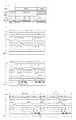
次に図5(a)〜(c)、図6を用いて、本実施形態の制御コンピュータによる段差補正処理について説明する。なお、本実施形態では、照射野Aで放射線又は光が照射される検出器の領域を第1の領域と、照射野Bで放射線又は光が照射される検出器の領域で第1の領域を除いた領域を第2の領域と称する。また、第1の領域に含まれる画素を第1の画素と、第2の領域に含まれる画素を第2の画素と称する。 Next, with reference to FIGS. 5A to 5C and FIG. 6, the step correction process by the control computer of this embodiment will be described. In the present embodiment, the detector region irradiated with radiation or light in the irradiation field A is a first region, and the detector region irradiated with radiation or light in the irradiation field B is a first region. The excluded area is referred to as a second area. In addition, a pixel included in the first region is referred to as a first pixel, and a pixel included in the second region is referred to as a second pixel.
まず、図5(a)〜(c)を用いて本発明の演算処理の基となる画像段差の発生メカニズムを説明する。図5(a)に示すように、本願発明者は、平面検出器の暗時出力が、放射線又は光の照射履歴に依存すること、より具体的には平面検出器の変換素子へバイアス電圧を印加した以後の放射線又は光の積分線量に依存することを見出した。本実施形態では照射野Aで撮影動作が行われているため、第2の画素の暗時出力は図5(a)中のAで示され、第1の画素の暗時出力はBで示される。そのため、例えば第2の画素の暗時出力Aと第1の画素の暗時出力Bに差が生じ、暗時出力の差が画像段差となる。特に、透視撮影の動作期間が長くなるほど、第1の画素と第2の画素の暗時出力差が大きくなり、画像上の段差がより顕著となる。図5(b)に示すように、平面検出器の暗時出力が、照射履歴に依存するため、平面検出器内で放射線又は光が照射される領域と照射されない領域の間で暗時出力に差が生じ、それにより画像段差が発生することを本願発明者は見出した。 First, the generation mechanism of the image level difference, which is the basis of the arithmetic processing of the present invention, will be described with reference to FIGS. As shown in FIG. 5A, the inventor of the present application determines that the dark output of the flat detector depends on the irradiation history of radiation or light, more specifically, applies a bias voltage to the conversion element of the flat detector. It was found that it depends on the integrated dose of radiation or light after application. In the present embodiment, since the photographing operation is performed in the irradiation field A, the dark output of the second pixel is indicated by A in FIG. 5A, and the dark output of the first pixel is indicated by B. It is. Therefore, for example, a difference occurs between the dark output A of the second pixel and the dark output B of the first pixel, and the difference in dark output becomes an image step. In particular, the longer the fluoroscopic operation period is, the larger the dark output difference between the first pixel and the second pixel becomes, and the step on the image becomes more prominent. As shown in FIG. 5B, since the dark-time output of the flat detector depends on the irradiation history, the dark-time output is set between the region irradiated with radiation or light and the non-irradiated region in the flat detector. The inventor of the present application has found that a difference is generated, thereby causing an image step.
そこで本願発明者は、放射線又は光の積分線量と画素の暗時出力特性に基づく暗時出力情報と、第1の画素への積分線量である第1の積分線量及び第2の画素への積分線量である第2の積分線量に基づいて、画像データを補正処理することを見出した。暗時出力情報としては、図5(a)のような積分線量と画素の暗時出力との関係を示した、積分線量−暗時出力特性を用いる。第1の積分線量により積分線量−暗時出力特性から第1の画素の暗時出力が特定され、第2の積分線量により積分線量−暗時出力特性から第2の画素の暗時出力が特定される。特定された暗時出力の値を用いて、画像データのうち第1の画素に相当するデータを補正し、また第2の画素に相当するデータを補正する。それにより、それぞれのデータに含まれる暗時出力が適切に低減され、第1の画素と第2の画素との間の暗時出力差が低減され、画像段差が低減される。本補正において、特定された暗時出力の差異を先に求め、第1の画素に相当するデータ若しくは第2の画素に相当するデータの一方のみにデータの補正を行ってもよい。 Therefore, the inventor of the present application provides dark output information based on the integrated dose of radiation or light and the dark output characteristics of the pixel, and the first integrated dose and the integration to the second pixel, which are integrated doses to the first pixel. It has been found that the image data is corrected based on the second integrated dose, which is a dose. As the dark output information, an integrated dose-dark output characteristic indicating the relationship between the integrated dose and the dark output of the pixel as shown in FIG. 5A is used. The first integrated dose specifies the dark output of the first pixel from the integrated dose-dark output characteristics, and the second integrated dose specifies the dark output of the second pixel from the integrated dose-dark output characteristics. Is done. Using the specified dark output value, the data corresponding to the first pixel in the image data is corrected, and the data corresponding to the second pixel is corrected. Thereby, the dark output included in each data is appropriately reduced, the dark output difference between the first pixel and the second pixel is reduced, and the image level difference is reduced. In this correction, the specified difference in dark output may be obtained first, and data correction may be performed on only one of the data corresponding to the first pixel or the data corresponding to the second pixel.
また高い精度のオフセット補正を行うためには、図5(b)のように、画像データが取得された後に暗画像データを取得し、それらを用いてオフセット補正処理を行うことが望ましい。そのようなオフセット補正処理を行った画像データには、画像データに含まれる暗時出力と暗画像データに含まれる暗時出力に差異があり、この差異に起因する補正を要する成分(以下補正量と称する)が含まれる。この補正量は、図5(b)、(c)に示すように、放射線や光の積分線量や放射線照射開始からの時間に依存して変動する。平面検出器の照射野が変更されると、平面検出器内で放射線又は光が照射される領域と照射されない領域の間で補正量に差異が生じ、それにより画像段差が発生することを本願発明者は見出した。 In order to perform offset correction with high accuracy, as shown in FIG. 5B, it is desirable to acquire dark image data after image data is acquired, and perform offset correction processing using them. The image data subjected to such offset correction processing has a difference between the dark output included in the image data and the dark output included in the dark image data, and a component (hereinafter referred to as a correction amount) that requires correction due to this difference. Called). As shown in FIGS. 5B and 5C, this correction amount varies depending on the integrated dose of radiation and light and the time from the start of radiation irradiation. When the irradiation field of the flat detector is changed, a difference in correction amount occurs between a region irradiated with radiation or light and a non-irradiated region in the flat detector, thereby causing an image step. Found.
そこで本補正においては、暗時出力情報としては、図5(c)のような積分線量と補正量との関係を示した、積分線量−補正量特性を用いてもよい。第1の積分線量により積分線量−補正量特性から第1の画素の補正量が特定され、第2の積分線量により積分線量補正量特性から第2の画素の補正量が特定される。特定された補正量の値を用いて、画像データのうち第1の画素に相当するデータを補正し、また第2の画素に相当するデータを補正する。それにより、それぞれのデータに含まれる暗時出力の差異が適切に低減され、第1の画素と第2の画素との間の補正量の差異が低減され、画像段差が低減される。本補正において、特定された補正量の差異を先に求め、第1の画素に相当するデータ若しくは第2の画素に相当するデータの一方のみにデータの補正を行ってもよい。 Therefore, in this correction, as the dark output information, an integrated dose-correction amount characteristic showing the relationship between the integrated dose and the correction amount as shown in FIG. 5C may be used. The correction amount of the first pixel is specified from the integrated dose-correction amount characteristic by the first integrated dose, and the correction amount of the second pixel is specified from the integrated dose correction amount characteristic by the second integrated dose. Using the specified value of the correction amount, data corresponding to the first pixel in the image data is corrected, and data corresponding to the second pixel is corrected. Thereby, a difference in dark output included in each data is appropriately reduced, a difference in correction amount between the first pixel and the second pixel is reduced, and an image step is reduced. In this correction, the difference between the specified correction amounts may be obtained first, and data correction may be performed on only one of the data corresponding to the first pixel or the data corresponding to the second pixel.
次に、図6を用いて本発明の補正処理を行う画像処理部を説明する。なお、図6(a)の画像処理部は、図1の信号処理部105内に含まれるものとして示されているが、本発明はそれに限定されるものではない。本発明の画像処理部は、図1の制御コンピュータ108に含まれていてもよい。 Next, an image processing unit that performs correction processing according to the present invention will be described with reference to FIG. Although the image processing unit in FIG. 6A is shown as being included in the
検出器104からの画像データは、記憶部602に含まれる画像データ記憶部603に一時記憶される。その後、検出器104からの暗画像データが取得され、オフセット補正部606が記憶部602の画像データと暗画像データとを用いてオフセット補正を行う。領域検出部608はオフセット補正された画像データに基づいて、第2の領域への放射線又は光の照射の有無を検知することにより、検出器104の放射線又は光が照射された照射領域を検出する。第2の領域への照射の有無だけでも照射野の変更を判定可能であるが、より確実に判定を行うために、第1の領域への放射線又は光の照射の有無を合わせて検出するようにしても良い。この照射領域を検出する方法としては、オフセット補正された画像データを予め定められた閾値と比較し、閾値よりもデータ値が大きい領域を照射領域として検出する。また、他の方法として、オフセット補正された画像データから微分値画像を作成し、微分値画像のピーク値を照射領域の境界とし、境界より内側の領域を照射領域として検出してもよい。また、制御コンピュータ108から放射線発生装置110の制御情報を取得し、制御情報に基づいて照射領域を検出してもよい。領域検出部608は、検出結果として照射領域情報を出力する。照射領域情報としては、例えば照射領域の4角の画素アドレスデータや、照射領域であることを示すフラグ、また、照射領域が切り替わった旨を示すフラグ等が適宜含まれる。 Image data from the
計測部607は、領域検出部608の検出結果に基づいて、オフセット補正された画像データから照射される放射線又は光の積分線量を計測する。具体的には、第1の領域に含まれる第1の画素に照射された放射線又は光の積分線量である第1の積分線量と、第2の領域に含まれる第2の画素に照射された放射線又は光の積分線量である第2の積分線量と、をそれぞれ計測する。積分線量は、各フレームの線量を積分して計測される。この積分線量としては、画素毎に計測しても良いし、領域毎の平均値から計測してもよい。 The
判定部609は、領域検出部608の検出結果に基づいて、第1の照射野から第2の照射野への変更の有無を判定する。判定方法としては、1つ前のフレームの照射領域情報と当該フレームの照射領域情報とを比較して判定する方法や、照射領域情報として照射領域が切り替わった旨を示すフラグが含まれている場合にはそれを直接用いて判定する方法が適宜用いられる。判定部609によって照射野の切替えが行われた旨(YES)の判定がなされた場合には、判定部609はオフセット補正された画像データを補正部に出力する。判定部609によって照射野の切替えが行われなかった旨(NO)の判定がなされた場合には、オフセット補正された画像データを後述するゲイン補正部611に出力する。 The
判定部609によって変更が有りと判定された場合、補正部610は記憶部602に含まれる暗時出力情報記憶部604から暗時出力情報を取得する。また、補正部610は計測部607によって計測された第1及び第2の積分線量を取得する。更に、補正部610は領域検出部608から照射領域に関する情報を取得する。これらの情報に基づいて補正部610は、オフセット補正された画像データのうち第1の画素のデータ及び第2の画素のデータのうちの少なくとも一方を補正する。具体的には、画像データに対し、暗時出力情報記憶部604から得られた暗時出力情報で加算処理又は減算処理を行う。 When the
本実施形態の暗時出力情報としては、図5(c)に示すような積分線量−補正量特性に基づくものであり、この特性を以下の近似式で示す。ここで、αは暗時出力特性係数であり、βは積分線量である。
補正量 = αexp(β)
暗時出力情報記憶部604は、上記近似式もしくは予め測定されたデータに基づいて、図6(b)に示すルックアップテーブルとして暗時出力情報を予め取得し記憶している。この暗時出力情報は、画素毎に準備してもよく、また全画素の平均値を用いて各画素に適用してもよい。また、撮像装置が、一般撮影や透視撮影等、特定のフレームレートが選択可能な異なる複数の撮影モードを実行可能な場合は、フレームレート毎に暗時出力情報を準備してもよい。暗時出力情報は、工場出荷時や製品検査時に予め取得され、暗時出力情報記憶部604に記憶されている。The dark output information of the present embodiment is based on an integral dose-correction amount characteristic as shown in FIG. 5C, and this characteristic is represented by the following approximate expression. Here, α is a dark output characteristic coefficient, and β is an integrated dose.
Correction amount = αexp (β)
The dark output
その後、画像データは記憶部602に含まれるゲイン補正用データ記憶部605に記憶されたゲイン補正用データを用いてゲイン補正部611でゲイン補正が行われる。各補正処理がなされた後、各補正処理がなされた画像データは信号処理部105から制御コンピュータ108に出力される。 Thereafter, the gain correction unit 611 performs gain correction on the image data using the gain correction data stored in the gain correction
このような補正を行うことにより、照射領域の影響を受けたゴースト(画像段差)を低減させ、著しく画質を低下させることなく照射領域の変動に対応することが可能となる。また、通常の撮影動作と同様の撮影動作により取得されたデータに基づいて補正処理がなされるため、照射野の切替えに際して補正データを取得するための特別な動作を行う必要がない。そのため、照射野の切替えに要する時間の短い撮像装置及びシステムを提供することが可能となる。 By performing such correction, it is possible to reduce the ghost (image step) affected by the irradiation region and cope with the variation of the irradiation region without significantly reducing the image quality. Further, since correction processing is performed based on data acquired by the same imaging operation as the normal imaging operation, it is not necessary to perform a special operation for acquiring correction data when switching the irradiation field. Therefore, it is possible to provide an imaging apparatus and system that require a short time for switching the irradiation field.
(第2の実施形態)
次に、図7を用いて、第2の実施形態に係る補正処理を行う画像処理部を説明する。第1の実施形態では、暗時出力情報を用いて段差補正処理を行ったが、第2の実施形態では、更に放射線又は光の積分線量と画素の明時(感度)出力特性に基づく明時出力情報を用いて段差補正処理を行う。その他は第1の実施形態と同様であり、以下では第1の実施形態と相違する点について詳細に説明し、第1の実施形態と同様な構成は同じ番号を付与して詳細な説明は割愛する。(Second Embodiment)
Next, an image processing unit that performs correction processing according to the second embodiment will be described with reference to FIG. In the first embodiment, the level difference correction processing is performed using the dark output information. However, in the second embodiment, the bright time based on the integrated dose of radiation or light and the bright time (sensitivity) output characteristics of the pixel. A level difference correction process is performed using the output information. Others are the same as those in the first embodiment, and the differences from the first embodiment will be described in detail below. The same configurations as those in the first embodiment are given the same numbers, and detailed descriptions are omitted. To do.
本実施形態において、記憶部602は更に明時出力情報記憶部701を含む。明時出力情報記憶部701が有する明時出力情報については後で詳細に説明する。また本実施形態において、補正部610が暗時出力段差補正部702と明時出力段差補正部703を含み、段差補正処理として、暗時出力情報を用いた加算又は減算処理と、明時出力情報を用いた除算処理を行い得る。明時出力段差補正部703は、第1の実施形態の補正部が行う加算又は減算処理を行う。明時出力段差補正部703は、明時出力情報記憶部701から明時出力情報を取得する。また、明時出力段差補正部703は計測部607によって計測された第1及び第2の積分線量を取得する。更に、明時出力段差補正部703は領域検出部608から照射領域に関する情報を取得する。これらの情報に基づいて明時出力段差補正部703は、暗時出力段差補正部702より補正された画像データのうち第1の画素のデータ及び第2の画素のデータのうちの少なくとも一方を補正する。具体的には、補正された画像データに対して、明時出力情報記憶部701から得られた明時出力情報で除算処理を行う。 In the present embodiment, the storage unit 602 further includes a light output information storage unit 701. The light output information included in the light output information storage unit 701 will be described in detail later. Further, in the present embodiment, the
次に、図8(a)〜(c)を用いて本実施形態の演算処理の基となる画像段差の他の発生メカニズムを説明する。図8(a)に示すように、本願発明者は、平面検出器の明時出力が、放射線又は光の照射履歴に依存すること、より具体的には平面検出器の変換素子へバイアス電圧を印加した以後の放射線又は光の積分線量に依存することを見出した。本実施形態では照射野Aで撮影動作が行われているため、第2の画素の明時出力は図5(a)中のAで示され、第1の画素の明時出力はBで示される。そのため、例えば明時出力Aと明時出力Bに差が生じ画像段差となる。特に、透視撮影の動作期間が長くなるほど、第1の画素と第2の画素の明時出力差が大きくなり、画像上の段差がより顕著となる。図8(b)に示すように、平面検出器内で放射線又は光が照射される領域と照射されない領域の間で明時出力に差が生じ、それにより画像段差が発生することを本願発明者は見出した。 Next, another generation mechanism of the image level difference that is the basis of the arithmetic processing according to the present embodiment will be described with reference to FIGS. As shown in FIG. 8A, the inventor of the present application determines that the light output of the flat detector depends on the irradiation history of radiation or light, more specifically, applies a bias voltage to the conversion element of the flat detector. It was found that it depends on the integrated dose of radiation or light after application. In the present embodiment, since the photographing operation is performed in the irradiation field A, the bright output of the second pixel is indicated by A in FIG. 5A, and the bright output of the first pixel is indicated by B. It is. Therefore, for example, a difference occurs between the bright output A and the bright output B, resulting in an image step. In particular, the longer the fluoroscopic operation period, the greater the difference in light output between the first pixel and the second pixel, and the step on the image becomes more prominent. As shown in FIG. 8 (b), the inventors of the present application show that a difference in light output occurs between a region irradiated with radiation or light and a region not irradiated in the flat detector, thereby generating an image step. Found.
そこで本願発明者は、放射線又は光の積分線量と画素の明時出力特性に基づく明時出力情報と、第1の画素への積分線量である第1の積分線量及び第2の画素への積分線量である第2の積分線量に基づいて、画像データを補正処理することを見出した。明時出力情報としては、図8(a)のような積分線量と画素の明時出力との関係を示した、積分線量−明時出力特性を用いる。第1の積分線量により積分線量−明時出力特性から第1の画素の明時出力が特定され、第2の積分線量により積分線量−明時出力特性から第2の画素の明時出力が特定される。特定された明時出力の値を用いて、画像データのうち第1の画素に相当するデータを補正し、また第2の画素に相当するデータを補正する。それにより、それぞれのデータに含まれる明時出力が適切に低減され、第1の画素と第2の画素との間の明時出力差が低減され、画像段差が低減される。本補正において、特定された明時出力の差異を先に求め、第1の画素に相当するデータ若しくは第2の画素に相当するデータの一方のみにデータの補正を行ってもよい。本補正において、明時出力情報としては、図8(c)のような積分線量と補正量との関係を示した、積分線量−補正量特性を用いてもよい。第1の積分線量により積分線量−補正量特性から第1の画素の補正量が特定され、第2の積分線量により積分線量補正量特性から第2の画素の補正量が特定される。特定された補正量の値を用いて、画像データのうち第1の画素に相当するデータを補正し、また第2の画素に相当するデータを補正する。それにより、それぞれのデータに含まれる暗時出力の差異が適切に低減され、第1の画素と第2の画素との間の補正量の差異が低減され、画像段差が低減される。本補正において、特定された補正量の差異を先に求め、第1の画素に相当するデータ若しくは第2の画素に相当するデータの一方のみにデータの補正を行ってもよい。明時出力情報は、暗時出力情報と同様に、ルックアップテーブルとして明時出力情報記憶部701に記憶されている。明時出力情報は、画素毎に準備してもよく、また全画素の平均値を用いて各画素に適用してもよい。また、撮像装置が、一般撮影や透視撮影等、特定のフレームレートが選択可能な異なる複数の撮影モードを実行可能な場合は、フレームレート毎に明時出力情報を準備してもよい。このように、更に明時出力情報を用いて段差補正を行うことにより、より高精度で画像段差を低減させることが可能となる。 Therefore, the inventor of the present application provides light output information based on the integrated dose of radiation or light and the light output characteristics of the pixel, and the integration of the first integrated dose and the second pixel, which are integrated doses to the first pixel. It has been found that the image data is corrected based on the second integrated dose, which is a dose. As the light output information, an integral dose-light output characteristic indicating the relationship between the integrated dose and the pixel light output as shown in FIG. 8A is used. The first integrated dose specifies the light output of the first pixel from the integrated dose-light output characteristics, and the second integrated dose specifies the light output of the second pixel from the integrated dose-light output characteristics. Is done. Using the specified light output value, the data corresponding to the first pixel in the image data is corrected, and the data corresponding to the second pixel is corrected. Thereby, the light output included in each data is appropriately reduced, the light output difference between the first pixel and the second pixel is reduced, and the image level difference is reduced. In this correction, the specified difference in light output may be obtained first, and data correction may be performed on only one of the data corresponding to the first pixel or the data corresponding to the second pixel. In this correction, as the light output information, an integrated dose-correction amount characteristic indicating the relationship between the integrated dose and the correction amount as shown in FIG. 8C may be used. The correction amount of the first pixel is specified from the integrated dose-correction amount characteristic by the first integrated dose, and the correction amount of the second pixel is specified from the integrated dose correction amount characteristic by the second integrated dose. Using the specified value of the correction amount, data corresponding to the first pixel in the image data is corrected, and data corresponding to the second pixel is corrected. Thereby, a difference in dark output included in each data is appropriately reduced, a difference in correction amount between the first pixel and the second pixel is reduced, and an image step is reduced. In this correction, the difference between the specified correction amounts may be obtained first, and data correction may be performed on only one of the data corresponding to the first pixel or the data corresponding to the second pixel. Similarly to the dark output information, the bright output information is stored in the bright output information storage unit 701 as a lookup table. The light output information may be prepared for each pixel, or may be applied to each pixel using an average value of all pixels. In addition, when the imaging apparatus can execute a plurality of different shooting modes in which a specific frame rate can be selected, such as general shooting or fluoroscopic shooting, light output information may be prepared for each frame rate. In this way, by further performing the step correction using the light output information, the image step can be reduced with higher accuracy.
なお、本発明の各実施形態は、例えば信号処理部105や制御コンピュータ108に含まれるコンピュータがプログラムを実行することによって実現することもできる。また、プログラムをコンピュータに供給するための手段、例えばかかるプログラムを記録したCD−ROM等のコンピュータ読み取り可能な記録媒体又はかかるプログラムを伝送するインターネット等の伝送媒体も本発明の実施形態として適用することができる。また、上記のプログラムも本発明の実施形態として適用することができる。上記のプログラム、記録媒体、伝送媒体及びプログラムプロダクトは、本発明の範疇に含まれる。また、第1又は第2の実施形態から容易に想像可能な組み合わせによる発明も本発明の範疇に含まれる。 Note that each embodiment of the present invention can also be realized by a computer included in the
100 撮像装置
101 検出部
102 駆動回路
103 読出回路
104 平面検出器
105 信号処理部
106 制御部
107 電源部
108 制御コンピュータ
109 放射線制御装置
110 放射線発生装置
111 放射線源
112 照射野絞り機構
113 表示装置DESCRIPTION OF
Claims (7)
Translated fromJapanese前記検出器は、第1の照射野で照射される第1の領域と、前記第1の照射野より広い第2の照射野で照射される領域で且つ前記第1の領域を除いた領域である第2の領域と、を含み、
前記画像処理部は、
前記放射線又は光の積分線量と前記画素の暗時出力特性に基づく暗時出力情報を記憶した記憶部と、
前記第1の領域に含まれる第1の画素に照射された放射線又は光の積分線量である第1の積分線量と、第2の領域に含まれる第2の画素に照射された放射線又は光の積分線量である第2の積分線量と、を計測する計測部と、
前記第1の照射野から前記第2の照射野への切替えが行われた場合、前記記憶部からの前記暗時出力情報と、前記計測部によって計測された前記第1及び第2の積分線量と、に基づいて、前記画像データのうち前記第1の画素のデータ及び前記第2の画素のデータのうちの少なくとも一方を補正する補正部と、
を含み、
前記画像処理部は、前記画像データと、前記検出器に放射線又は光の照射が行われない暗状態で前記検出器から前記画像データの後に出力された暗画像データと、を用いてオフセット補正処理を行い、前記第1の照射野から前記第2の照射野への切替えが行われた場合、前記暗時出力情報と前記第1及び第2の積分線量とに基づいて、オフセット補正処理された前記画像データのうち前記第1の画素のデータ及び前記第2の画素のデータのうちの少なくとも一方を補正することを特徴とする撮像システム。Radiation or pixel having a conversion element for converting thelight corresponding to the radiation charge is more arranged, a detector for outputting image data corresponding to the applied radiation or light, an image for performing image processing of the image data An imaging system including a processing unit,
The detector includes a first region irradiated in a first irradiation field, a region irradiated in a second irradiation field wider than the first irradiation field, and a region excluding the first region. A second region, and
The image processing unit
A storage unit storing dark output information based on an integrated dose of the radiation or light and a dark output characteristic of the pixel;
The first integrated dose, which is the integrated dose of radiation or light irradiated to the first pixel included in the first region, and the radiation or light irradiated to the second pixel included in the second region. A measurement unit that measures a second integrated dose that is an integrated dose; and
When the switching from the first irradiation field to the second irradiation field is performed, the dark output information from the storage unit and the first and second integrated doses measured by the measurement unit And a correction unit that corrects at least one of the data of the first pixel and the data of the second pixel among the image data,
Including
The image processing unit uses the image data and dark image data output after the image data from the detector in a dark state in which the detector is not irradiated with radiation or light. When the switching from the first irradiation field to the second irradiation field is performed, an offset correction process is performed based on the dark output information and the first and second integrated doses. An image pickup system that corrects at least one of data of the first pixel and data of the second pixel in the image data.
前記補正部は、前記記憶部からの前記明時出力情報と、前記計測部によって計測された前記第1及び第2の積分線量と、に基づいて、前記暗時出力情報と第1及び第2の積分線量とに基づいて補正されたデータを更に補正することを特徴とする請求項1に記載の撮像システム。The storage unit further stores light output information based on an integrated dose of the radiation or light and a light output characteristic of the pixel,
The correction unit is configured to output the dark output information and the first and second based on the light output information from the storage unit and the first and second integrated doses measured by the measurement unit. The imaging system according to claim 1, further comprising correcting the corrected data based on the integrated dose.
前記検出器に前記放射線又は光が第1の照射野で照射される第1の領域に含まれる第1の画素に照射された放射線又は光の積分線量である第1の積分線量と、前記第1の照射野より広い第2の照射野で照射される領域で且つ前記第1の領域を除いた領域である第2の領域に含まれる第2の画素に照射された放射線又は光の積分線量である第2の積分線量と、を計測する計測工程と、
前記第1の照射野から前記第2の照射野への切替えが行われた場合、前記放射線又は光の積分線量と、予め取得された前記画素の暗時出力特性に基づく暗時出力情報と、計測された前記第1及び第2の積分線量と、に基づいて、前記画像データのうち前記第1の画素のデータ及び前記第2の画素のデータのうちの少なくとも一方を補正する補正工程と、
を行い、
前記補正工程は、前記画像データと、前記検出器に放射線又は光の照射が行われない暗状態で前記検出器から前記画像データの後に出力された暗画像データと、を用いたオフセット補正処理が行われ、前記第1の照射野から前記第2の照射野への切替えが行われた場合、前記暗時出力情報と前記第1及び第2の積分線量とに基づいて、オフセット補正処理された前記画像データのうち前記第1の画素のデータ及び前記第2の画素のデータのうちの少なくとも一方を補正することを特徴とする画像処理方法。Radiation or pixel having a conversion element for converting thelight corresponding to the radiation charge is more disposed, the image processing of the image data acquired from the detector for outputting image data corresponding to the applied radiation or light An image processing method to perform,
A first integrated dose that is an integrated dose of radiation or light irradiated to a first pixel included in a first region where the detector is irradiated with the radiation or light in a first irradiation field; An integrated dose of radiation or light irradiated to a second pixel included in a second region which is a region irradiated in a second irradiation field wider than one irradiation field and which is a region excluding the first region. A measuring step for measuring a second integrated dose that is
When switching from the first irradiation field to the second irradiation field, the integrated dose of the radiation or light, dark output information based on the dark output characteristics of the pixel acquired in advance, A correction step of correcting at least one of the first pixel data and the second pixel data among the image data based on the measured first and second integrated doses;
And
The correction step includes an offset correction process using the image data and dark image data output after the image data from the detector in a dark state where the detector is not irradiated with radiation or light. When the switching from the first irradiation field to the second irradiation field was performed, an offset correction process was performed based on the dark output information and the first and second integrated doses. An image processing method comprising correcting at least one of data of the first pixel and data of the second pixel in the image data.
前記検出器に前記放射線又は光が第1の照射野で照射される第1の領域に含まれる第1の画素に照射された放射線又は光の積分線量である第1の積分線量と、前記第1の照射野より広い第2の照射野で照射される領域で且つ前記第1の領域を除いた領域である第2の領域に含まれる第2の画素に照射された放射線又は光の積分線量である第2の積分線量と、を計測する計測工程と、
前記第1の照射野から前記第2の照射野への切替えが行われた場合、前記放射線又は光の積分線量と、予め取得された前記画素の暗時出力特性に基づく暗時出力情報と、計測された前記第1及び第2の積分線量と、に基づいて、前記画像データのうち前記第1の画素のデータ及び前記第2の画素のデータのうちの少なくとも一方を補正する補正工程と、
をコンピュータに実行させ、
前記補正工程は、前記画像データと、前記検出器に放射線又は光の照射が行われない暗状態で前記検出器から前記画像データの後に出力された暗画像データと、を用いたオフセット補正処理が行われ、前記第1の照射野から前記第2の照射野への切替えが行われた場合、前記暗時出力情報と前記第1及び第2の積分線量とに基づいて、オフセット補正処理された前記画像データのうち前記第1の画素のデータ及び前記第2の画素のデータのうちの少なくとも一方を補正することを特徴とするプログラム。Radiation or pixel having a conversion element for converting thelight corresponding to the radiation charge is more disposed, the image processing of the image data acquired from the detector for outputting image data corresponding to the applied radiation or light A program to be executed by a computer,
A first integrated dose that is an integrated dose of radiation or light irradiated to a first pixel included in a first region where the detector is irradiated with the radiation or light in a first irradiation field; An integrated dose of radiation or light irradiated to a second pixel included in a second region which is a region irradiated in a second irradiation field wider than one irradiation field and which is a region excluding the first region. A measuring step for measuring a second integrated dose that is
When switching from the first irradiation field to the second irradiation field, the integrated dose of the radiation or light, dark output information based on the dark output characteristics of the pixel acquired in advance, Acorrection step of correcting at least one of the first pixel data and the second pixel data among the image data based on the measured first and second integrated doses;
To the computer,
The correction step includes an offset correction process using the image data and dark image data output after the image data from the detector in a dark state where the detector is not irradiated with radiation or light. When the switching from the first irradiation field to the second irradiation field was performed, an offset correction process was performed based on the dark output information and the first and second integrated doses. A program for correcting at least one of data of the first pixel and data of the second pixel in the image data.
Priority Applications (4)
| Application Number | Priority Date | Filing Date | Title |
|---|---|---|---|
| JP2009195698AJP5448643B2 (en) | 2009-08-26 | 2009-08-26 | Imaging system, image processing method thereof, and program thereof |
| CN2010800369919ACN102481130A (en) | 2009-08-26 | 2010-08-25 | Imaging system, image processing method therefor, and program therefor |
| US13/390,592US8541754B2 (en) | 2009-08-26 | 2010-08-25 | Imaging system, image processing method therefor, and program therefor |
| PCT/JP2010/005231WO2011024448A1 (en) | 2009-08-26 | 2010-08-25 | Imaging system, image processing method therefor, and program therefor |
Applications Claiming Priority (1)
| Application Number | Priority Date | Filing Date | Title |
|---|---|---|---|
| JP2009195698AJP5448643B2 (en) | 2009-08-26 | 2009-08-26 | Imaging system, image processing method thereof, and program thereof |
Publications (2)
| Publication Number | Publication Date |
|---|---|
| JP2011045492A JP2011045492A (en) | 2011-03-10 |
| JP5448643B2true JP5448643B2 (en) | 2014-03-19 |
Family
ID=43627568
Family Applications (1)
| Application Number | Title | Priority Date | Filing Date |
|---|---|---|---|
| JP2009195698AExpired - Fee RelatedJP5448643B2 (en) | 2009-08-26 | 2009-08-26 | Imaging system, image processing method thereof, and program thereof |
Country Status (4)
| Country | Link |
|---|---|
| US (1) | US8541754B2 (en) |
| JP (1) | JP5448643B2 (en) |
| CN (1) | CN102481130A (en) |
| WO (1) | WO2011024448A1 (en) |
Families Citing this family (13)
| Publication number | Priority date | Publication date | Assignee | Title |
|---|---|---|---|---|
| DE102010033609B3 (en)* | 2010-08-06 | 2011-12-22 | Siemens Aktiengesellschaft | Method for estimating dosage of X-ray radiation on examination object e.g. human body, involves determining total dosage of X-ray radiation by accumulation of initial and successive dosage values of X-ray radiation in chamber |
| GB2522347B (en)* | 2012-07-24 | 2016-03-09 | Canon Kk | Imaging apparatus, radiation imaging apparatus, and method for controlling the same |
| US9279893B2 (en)* | 2012-07-24 | 2016-03-08 | Canon Kabushiki Kaisha | Radiation imaging control apparatus, radiation imaging system and radiation imaging apparatus, and method for controlling the same |
| JP6525579B2 (en)* | 2014-12-22 | 2019-06-05 | キヤノン株式会社 | Radiation imaging apparatus and radiation imaging system |
| JP6455337B2 (en)* | 2015-06-25 | 2019-01-23 | コニカミノルタ株式会社 | Radiographic imaging system and radiographic imaging device |
| US10416323B2 (en) | 2016-03-29 | 2019-09-17 | Canon Kabushiki Kaisha | Radiation imaging apparatus, radiation imaging system, and method of operating radiation imaging apparatus |
| JP6417368B2 (en)* | 2016-03-29 | 2018-11-07 | キヤノン株式会社 | Radiation imaging apparatus and radiation imaging system |
| JP6400053B2 (en)* | 2016-07-22 | 2018-10-03 | キヤノン株式会社 | Radiation imaging apparatus, radiation imaging system, control method thereof, and program thereof |
| JP6951158B2 (en)* | 2017-09-05 | 2021-10-20 | キヤノン株式会社 | Radiation imaging device, its driving method and radiation imaging system |
| JP6925294B2 (en)* | 2018-03-23 | 2021-08-25 | 富士フイルム株式会社 | Image processing equipment, radiation imaging system, image processing method, and image processing program |
| JP7344769B2 (en)* | 2019-11-22 | 2023-09-14 | キヤノン株式会社 | Radiation detection device and output method |
| CN111887875B (en)* | 2020-08-21 | 2024-04-23 | 上海联影医疗科技股份有限公司 | PET device correction method, PET device correction device, computer device and storage medium |
| JP7449260B2 (en)* | 2021-04-15 | 2024-03-13 | キヤノン株式会社 | Radiation imaging device and radiation imaging system |
Family Cites Families (16)
| Publication number | Priority date | Publication date | Assignee | Title |
|---|---|---|---|---|
| US5920070A (en)* | 1996-11-27 | 1999-07-06 | General Electric Company | Solid state area x-ray detector with adjustable bias |
| JP3275803B2 (en) | 1997-10-30 | 2002-04-22 | 株式会社島津製作所 | X-ray diagnostic equipment |
| EP1121719A4 (en)* | 1999-07-26 | 2007-08-22 | Edge Medical Devices Ltd | DIGITAL DETECTOR FOR X-RAY RECORDING |
| JP2004020300A (en)* | 2002-06-14 | 2004-01-22 | Toshiba Corp | Radiation diagnostic equipment |
| US7065177B2 (en)* | 2002-11-14 | 2006-06-20 | General Electric Company | Method and apparatus for correcting a retained image artifact |
| US6920198B2 (en) | 2003-05-02 | 2005-07-19 | Ge Medical Systems Global Technology Company, Llc | Methods and apparatus for processing a fluoroscopic image |
| JP3942178B2 (en)* | 2003-07-29 | 2007-07-11 | ジーイー・メディカル・システムズ・グローバル・テクノロジー・カンパニー・エルエルシー | X-ray CT system |
| JP2006068512A (en)* | 2004-08-06 | 2006-03-16 | Canon Inc | Imaging apparatus, imaging system, imaging method, and computer program |
| US7233005B2 (en)* | 2005-02-16 | 2007-06-19 | Hologic, Inc. | Amorphous selenium flat panel x-ray imager for tomosynthesis and static imaging |
| JP2006239117A (en)* | 2005-03-03 | 2006-09-14 | Konica Minolta Holdings Inc | Radiographic device |
| CN1881075B (en)* | 2005-06-15 | 2011-08-03 | 上海医疗器械厂有限公司 | X-ray digital imaging correction method |
| JP5057543B2 (en)* | 2006-02-16 | 2012-10-24 | キヤノン株式会社 | Image processing apparatus, control method therefor, and program |
| JP4807846B2 (en) | 2006-07-26 | 2011-11-02 | 株式会社日立メディコ | X-ray diagnostic imaging equipment |
| JP4945249B2 (en)* | 2007-01-10 | 2012-06-06 | 株式会社東芝 | X-ray transmission image display system |
| JP5455312B2 (en)* | 2007-03-13 | 2014-03-26 | キヤノン株式会社 | Radiation imaging apparatus, control method thereof, and program |
| JP5105940B2 (en)* | 2007-04-06 | 2012-12-26 | キヤノン株式会社 | Imaging apparatus, imaging system, control method thereof, and program |
- 2009
- 2009-08-26JPJP2009195698Apatent/JP5448643B2/ennot_activeExpired - Fee Related
- 2010
- 2010-08-25WOPCT/JP2010/005231patent/WO2011024448A1/enactiveApplication Filing
- 2010-08-25USUS13/390,592patent/US8541754B2/ennot_activeExpired - Fee Related
- 2010-08-25CNCN2010800369919Apatent/CN102481130A/enactivePending
Also Published As
| Publication number | Publication date |
|---|---|
| CN102481130A (en) | 2012-05-30 |
| JP2011045492A (en) | 2011-03-10 |
| US8541754B2 (en) | 2013-09-24 |
| WO2011024448A1 (en) | 2011-03-03 |
| US20120138811A1 (en) | 2012-06-07 |
Similar Documents
| Publication | Publication Date | Title |
|---|---|---|
| JP5448643B2 (en) | Imaging system, image processing method thereof, and program thereof | |
| JP5792923B2 (en) | Radiation imaging apparatus, radiation imaging system, control method thereof, and program thereof | |
| JP5517484B2 (en) | Imaging apparatus and imaging system, control method thereof, and program thereof | |
| JP5274661B2 (en) | Radiation imaging apparatus, radiation imaging system, control method thereof, and program thereof | |
| JP5642166B2 (en) | Imaging system and control method thereof | |
| JP5566209B2 (en) | Imaging apparatus and imaging system, control method thereof, and program thereof | |
| JP5361628B2 (en) | Imaging apparatus and imaging system, control method thereof, and program thereof | |
| JP5539139B2 (en) | IMAGING DEVICE, IMAGING SYSTEM, AND IMAGING DEVICE CONTROL METHOD | |
| US8792022B2 (en) | Image pickup apparatus, image pickup system, and method of controlling them | |
| JP5398846B2 (en) | Imaging apparatus and imaging system, control method thereof, and program thereof | |
| JP6061865B2 (en) | IMAGING DEVICE, IMAGING SYSTEM, AND IMAGING DEVICE CONTROL METHOD | |
| US20120241634A1 (en) | Image pickup apparatus, image pickup system, and method of controlling them | |
| JP2010141715A (en) | Image capturing apparatus and system | |
| JP5784086B2 (en) | Imaging apparatus and imaging system, control method thereof, and program thereof |
Legal Events
| Date | Code | Title | Description |
|---|---|---|---|
| A621 | Written request for application examination | Free format text:JAPANESE INTERMEDIATE CODE: A621 Effective date:20120713 | |
| A131 | Notification of reasons for refusal | Free format text:JAPANESE INTERMEDIATE CODE: A131 Effective date:20130528 | |
| A521 | Request for written amendment filed | Free format text:JAPANESE INTERMEDIATE CODE: A523 Effective date:20130729 | |
| A131 | Notification of reasons for refusal | Free format text:JAPANESE INTERMEDIATE CODE: A131 Effective date:20130820 | |
| A521 | Request for written amendment filed | Free format text:JAPANESE INTERMEDIATE CODE: A523 Effective date:20131021 | |
| TRDD | Decision of grant or rejection written | ||
| A01 | Written decision to grant a patent or to grant a registration (utility model) | Free format text:JAPANESE INTERMEDIATE CODE: A01 Effective date:20131126 | |
| A61 | First payment of annual fees (during grant procedure) | Free format text:JAPANESE INTERMEDIATE CODE: A61 Effective date:20131224 | |
| R151 | Written notification of patent or utility model registration | Ref document number:5448643 Country of ref document:JP Free format text:JAPANESE INTERMEDIATE CODE: R151 | |
| LAPS | Cancellation because of no payment of annual fees |