JP5442777B2 - Package structure and manufacturing method thereof - Google Patents
Package structure and manufacturing method thereofDownload PDFInfo
- Publication number
- JP5442777B2 JP5442777B2JP2012003203AJP2012003203AJP5442777B2JP 5442777 B2JP5442777 B2JP 5442777B2JP 2012003203 AJP2012003203 AJP 2012003203AJP 2012003203 AJP2012003203 AJP 2012003203AJP 5442777 B2JP5442777 B2JP 5442777B2
- Authority
- JP
- Japan
- Prior art keywords
- layer
- pattern
- chip
- package structure
- pattern circuit
- Prior art date
- Legal status (The legal status is an assumption and is not a legal conclusion. Google has not performed a legal analysis and makes no representation as to the accuracy of the status listed.)
- Expired - Fee Related
Links
- 238000004519manufacturing processMethods0.000titleclaimsdescription30
- 239000010410layerSubstances0.000claimsdescription229
- 229910052751metalInorganic materials0.000claimsdescription59
- 239000002184metalSubstances0.000claimsdescription59
- 239000000758substrateSubstances0.000claimsdescription44
- 238000000034methodMethods0.000claimsdescription34
- 239000011241protective layerSubstances0.000claimsdescription21
- PXHVJJICTQNCMI-UHFFFAOYSA-NNickelChemical compound[Ni]PXHVJJICTQNCMI-UHFFFAOYSA-N0.000claimsdescription16
- 239000008393encapsulating agentSubstances0.000claimsdescription15
- PCHJSUWPFVWCPO-UHFFFAOYSA-NgoldChemical compound[Au]PCHJSUWPFVWCPO-UHFFFAOYSA-N0.000claimsdescription12
- 229910052737goldInorganic materials0.000claimsdescription12
- 239000010931goldSubstances0.000claimsdescription12
- 239000003566sealing materialSubstances0.000claimsdescription12
- 229910052759nickelInorganic materials0.000claimsdescription8
- 238000009713electroplatingMethods0.000claimsdescription7
- BQCADISMDOOEFD-UHFFFAOYSA-NSilverChemical compound[Ag]BQCADISMDOOEFD-UHFFFAOYSA-N0.000claimsdescription6
- BSIDXUHWUKTRQL-UHFFFAOYSA-Nnickel palladiumChemical compound[Ni].[Pd]BSIDXUHWUKTRQL-UHFFFAOYSA-N0.000claimsdescription6
- 229910052709silverInorganic materials0.000claimsdescription6
- 239000004332silverSubstances0.000claimsdescription6
- 238000005530etchingMethods0.000claimsdescription4
- 229910045601alloyInorganic materials0.000claimsdescription3
- 239000000956alloySubstances0.000claimsdescription3
- 239000000126substanceSubstances0.000claimsdescription2
- 239000011162core materialSubstances0.000description11
- 239000000463materialSubstances0.000description7
- 230000017525heat dissipationEffects0.000description4
- 238000007747platingMethods0.000description3
- 239000000654additiveSubstances0.000description2
- 229910000838Al alloyInorganic materials0.000description1
- RYGMFSIKBFXOCR-UHFFFAOYSA-NCopperChemical compound[Cu]RYGMFSIKBFXOCR-UHFFFAOYSA-N0.000description1
- 229910000881Cu alloyInorganic materials0.000description1
- 230000000996additive effectEffects0.000description1
- 229910052782aluminiumInorganic materials0.000description1
- XAGFODPZIPBFFR-UHFFFAOYSA-NaluminiumChemical compound[Al]XAGFODPZIPBFFR-UHFFFAOYSA-N0.000description1
- 229910052802copperInorganic materials0.000description1
- 239000010949copperSubstances0.000description1
- 238000012986modificationMethods0.000description1
- 230000004048modificationEffects0.000description1
- 230000000149penetrating effectEffects0.000description1
- 239000004065semiconductorSubstances0.000description1
Images


Classifications
- H—ELECTRICITY
- H01—ELECTRIC ELEMENTS
- H01L—SEMICONDUCTOR DEVICES NOT COVERED BY CLASS H10
- H01L21/00—Processes or apparatus adapted for the manufacture or treatment of semiconductor or solid state devices or of parts thereof
- H01L21/02—Manufacture or treatment of semiconductor devices or of parts thereof
- H01L21/04—Manufacture or treatment of semiconductor devices or of parts thereof the devices having potential barriers, e.g. a PN junction, depletion layer or carrier concentration layer
- H01L21/50—Assembly of semiconductor devices using processes or apparatus not provided for in a single one of the groups H01L21/18 - H01L21/326 or H10D48/04 - H10D48/07 e.g. sealing of a cap to a base of a container
- H01L21/56—Encapsulations, e.g. encapsulation layers, coatings
- H01L21/563—Encapsulation of active face of flip-chip device, e.g. underfilling or underencapsulation of flip-chip, encapsulation preform on chip or mounting substrate
- H—ELECTRICITY
- H01—ELECTRIC ELEMENTS
- H01L—SEMICONDUCTOR DEVICES NOT COVERED BY CLASS H10
- H01L21/00—Processes or apparatus adapted for the manufacture or treatment of semiconductor or solid state devices or of parts thereof
- H01L21/02—Manufacture or treatment of semiconductor devices or of parts thereof
- H01L21/04—Manufacture or treatment of semiconductor devices or of parts thereof the devices having potential barriers, e.g. a PN junction, depletion layer or carrier concentration layer
- H01L21/48—Manufacture or treatment of parts, e.g. containers, prior to assembly of the devices, using processes not provided for in a single one of the groups H01L21/18 - H01L21/326 or H10D48/04 - H10D48/07
- H01L21/4814—Conductive parts
- H01L21/4821—Flat leads, e.g. lead frames with or without insulating supports
- H—ELECTRICITY
- H01—ELECTRIC ELEMENTS
- H01L—SEMICONDUCTOR DEVICES NOT COVERED BY CLASS H10
- H01L21/00—Processes or apparatus adapted for the manufacture or treatment of semiconductor or solid state devices or of parts thereof
- H01L21/02—Manufacture or treatment of semiconductor devices or of parts thereof
- H01L21/04—Manufacture or treatment of semiconductor devices or of parts thereof the devices having potential barriers, e.g. a PN junction, depletion layer or carrier concentration layer
- H01L21/50—Assembly of semiconductor devices using processes or apparatus not provided for in a single one of the groups H01L21/18 - H01L21/326 or H10D48/04 - H10D48/07 e.g. sealing of a cap to a base of a container
- H01L21/56—Encapsulations, e.g. encapsulation layers, coatings
- H01L21/568—Temporary substrate used as encapsulation process aid
- H—ELECTRICITY
- H01—ELECTRIC ELEMENTS
- H01L—SEMICONDUCTOR DEVICES NOT COVERED BY CLASS H10
- H01L23/00—Details of semiconductor or other solid state devices
- H01L23/48—Arrangements for conducting electric current to or from the solid state body in operation, e.g. leads, terminal arrangements ; Selection of materials therefor
- H01L23/488—Arrangements for conducting electric current to or from the solid state body in operation, e.g. leads, terminal arrangements ; Selection of materials therefor consisting of soldered or bonded constructions
- H01L23/495—Lead-frames or other flat leads
- H01L23/49579—Lead-frames or other flat leads characterised by the materials of the lead frames or layers thereon
- H01L23/49582—Metallic layers on lead frames
- H—ELECTRICITY
- H01—ELECTRIC ELEMENTS
- H01L—SEMICONDUCTOR DEVICES NOT COVERED BY CLASS H10
- H01L2224/00—Indexing scheme for arrangements for connecting or disconnecting semiconductor or solid-state bodies and methods related thereto as covered by H01L24/00
- H01L2224/01—Means for bonding being attached to, or being formed on, the surface to be connected, e.g. chip-to-package, die-attach, "first-level" interconnects; Manufacturing methods related thereto
- H01L2224/26—Layer connectors, e.g. plate connectors, solder or adhesive layers; Manufacturing methods related thereto
- H01L2224/31—Structure, shape, material or disposition of the layer connectors after the connecting process
- H01L2224/32—Structure, shape, material or disposition of the layer connectors after the connecting process of an individual layer connector
- H01L2224/321—Disposition
- H01L2224/32151—Disposition the layer connector connecting between a semiconductor or solid-state body and an item not being a semiconductor or solid-state body, e.g. chip-to-substrate, chip-to-passive
- H01L2224/32221—Disposition the layer connector connecting between a semiconductor or solid-state body and an item not being a semiconductor or solid-state body, e.g. chip-to-substrate, chip-to-passive the body and the item being stacked
- H01L2224/32245—Disposition the layer connector connecting between a semiconductor or solid-state body and an item not being a semiconductor or solid-state body, e.g. chip-to-substrate, chip-to-passive the body and the item being stacked the item being metallic
- H—ELECTRICITY
- H01—ELECTRIC ELEMENTS
- H01L—SEMICONDUCTOR DEVICES NOT COVERED BY CLASS H10
- H01L2224/00—Indexing scheme for arrangements for connecting or disconnecting semiconductor or solid-state bodies and methods related thereto as covered by H01L24/00
- H01L2224/01—Means for bonding being attached to, or being formed on, the surface to be connected, e.g. chip-to-package, die-attach, "first-level" interconnects; Manufacturing methods related thereto
- H01L2224/42—Wire connectors; Manufacturing methods related thereto
- H01L2224/47—Structure, shape, material or disposition of the wire connectors after the connecting process
- H01L2224/48—Structure, shape, material or disposition of the wire connectors after the connecting process of an individual wire connector
- H01L2224/4805—Shape
- H01L2224/4809—Loop shape
- H01L2224/48091—Arched
- H—ELECTRICITY
- H01—ELECTRIC ELEMENTS
- H01L—SEMICONDUCTOR DEVICES NOT COVERED BY CLASS H10
- H01L2224/00—Indexing scheme for arrangements for connecting or disconnecting semiconductor or solid-state bodies and methods related thereto as covered by H01L24/00
- H01L2224/01—Means for bonding being attached to, or being formed on, the surface to be connected, e.g. chip-to-package, die-attach, "first-level" interconnects; Manufacturing methods related thereto
- H01L2224/42—Wire connectors; Manufacturing methods related thereto
- H01L2224/47—Structure, shape, material or disposition of the wire connectors after the connecting process
- H01L2224/48—Structure, shape, material or disposition of the wire connectors after the connecting process of an individual wire connector
- H01L2224/481—Disposition
- H01L2224/48151—Connecting between a semiconductor or solid-state body and an item not being a semiconductor or solid-state body, e.g. chip-to-substrate, chip-to-passive
- H01L2224/48221—Connecting between a semiconductor or solid-state body and an item not being a semiconductor or solid-state body, e.g. chip-to-substrate, chip-to-passive the body and the item being stacked
- H01L2224/48245—Connecting between a semiconductor or solid-state body and an item not being a semiconductor or solid-state body, e.g. chip-to-substrate, chip-to-passive the body and the item being stacked the item being metallic
- H01L2224/48247—Connecting between a semiconductor or solid-state body and an item not being a semiconductor or solid-state body, e.g. chip-to-substrate, chip-to-passive the body and the item being stacked the item being metallic connecting the wire to a bond pad of the item
- H—ELECTRICITY
- H01—ELECTRIC ELEMENTS
- H01L—SEMICONDUCTOR DEVICES NOT COVERED BY CLASS H10
- H01L2224/00—Indexing scheme for arrangements for connecting or disconnecting semiconductor or solid-state bodies and methods related thereto as covered by H01L24/00
- H01L2224/73—Means for bonding being of different types provided for in two or more of groups H01L2224/10, H01L2224/18, H01L2224/26, H01L2224/34, H01L2224/42, H01L2224/50, H01L2224/63, H01L2224/71
- H01L2224/732—Location after the connecting process
- H01L2224/73251—Location after the connecting process on different surfaces
- H01L2224/73265—Layer and wire connectors
- H—ELECTRICITY
- H01—ELECTRIC ELEMENTS
- H01L—SEMICONDUCTOR DEVICES NOT COVERED BY CLASS H10
- H01L2224/00—Indexing scheme for arrangements for connecting or disconnecting semiconductor or solid-state bodies and methods related thereto as covered by H01L24/00
- H01L2224/80—Methods for connecting semiconductor or other solid state bodies using means for bonding being attached to, or being formed on, the surface to be connected
- H01L2224/85—Methods for connecting semiconductor or other solid state bodies using means for bonding being attached to, or being formed on, the surface to be connected using a wire connector
- H01L2224/85001—Methods for connecting semiconductor or other solid state bodies using means for bonding being attached to, or being formed on, the surface to be connected using a wire connector involving a temporary auxiliary member not forming part of the bonding apparatus, e.g. removable or sacrificial coating, film or substrate
- H—ELECTRICITY
- H01—ELECTRIC ELEMENTS
- H01L—SEMICONDUCTOR DEVICES NOT COVERED BY CLASS H10
- H01L24/00—Arrangements for connecting or disconnecting semiconductor or solid-state bodies; Methods or apparatus related thereto
- H01L24/01—Means for bonding being attached to, or being formed on, the surface to be connected, e.g. chip-to-package, die-attach, "first-level" interconnects; Manufacturing methods related thereto
- H01L24/42—Wire connectors; Manufacturing methods related thereto
- H01L24/47—Structure, shape, material or disposition of the wire connectors after the connecting process
- H01L24/48—Structure, shape, material or disposition of the wire connectors after the connecting process of an individual wire connector
- H—ELECTRICITY
- H01—ELECTRIC ELEMENTS
- H01L—SEMICONDUCTOR DEVICES NOT COVERED BY CLASS H10
- H01L24/00—Arrangements for connecting or disconnecting semiconductor or solid-state bodies; Methods or apparatus related thereto
- H01L24/73—Means for bonding being of different types provided for in two or more of groups H01L24/10, H01L24/18, H01L24/26, H01L24/34, H01L24/42, H01L24/50, H01L24/63, H01L24/71
- H—ELECTRICITY
- H01—ELECTRIC ELEMENTS
- H01L—SEMICONDUCTOR DEVICES NOT COVERED BY CLASS H10
- H01L2924/00—Indexing scheme for arrangements or methods for connecting or disconnecting semiconductor or solid-state bodies as covered by H01L24/00
- H01L2924/0001—Technical content checked by a classifier
- H01L2924/00014—Technical content checked by a classifier the subject-matter covered by the group, the symbol of which is combined with the symbol of this group, being disclosed without further technical details
- H—ELECTRICITY
- H01—ELECTRIC ELEMENTS
- H01L—SEMICONDUCTOR DEVICES NOT COVERED BY CLASS H10
- H01L2924/00—Indexing scheme for arrangements or methods for connecting or disconnecting semiconductor or solid-state bodies as covered by H01L24/00
- H01L2924/10—Details of semiconductor or other solid state devices to be connected
- H01L2924/11—Device type
- H01L2924/12—Passive devices, e.g. 2 terminal devices
- H01L2924/1204—Optical Diode
- H01L2924/12041—LED
- H—ELECTRICITY
- H01—ELECTRIC ELEMENTS
- H01L—SEMICONDUCTOR DEVICES NOT COVERED BY CLASS H10
- H01L2924/00—Indexing scheme for arrangements or methods for connecting or disconnecting semiconductor or solid-state bodies as covered by H01L24/00
- H01L2924/10—Details of semiconductor or other solid state devices to be connected
- H01L2924/11—Device type
- H01L2924/12—Passive devices, e.g. 2 terminal devices
- H01L2924/1204—Optical Diode
- H01L2924/12042—LASER
- H—ELECTRICITY
- H01—ELECTRIC ELEMENTS
- H01L—SEMICONDUCTOR DEVICES NOT COVERED BY CLASS H10
- H01L2924/00—Indexing scheme for arrangements or methods for connecting or disconnecting semiconductor or solid-state bodies as covered by H01L24/00
- H01L2924/15—Details of package parts other than the semiconductor or other solid state devices to be connected
- H01L2924/181—Encapsulation
- H—ELECTRICITY
- H01—ELECTRIC ELEMENTS
- H01L—SEMICONDUCTOR DEVICES NOT COVERED BY CLASS H10
- H01L2924/00—Indexing scheme for arrangements or methods for connecting or disconnecting semiconductor or solid-state bodies as covered by H01L24/00
- H01L2924/30—Technical effects
- H01L2924/301—Electrical effects
- H01L2924/3025—Electromagnetic shielding
- Y—GENERAL TAGGING OF NEW TECHNOLOGICAL DEVELOPMENTS; GENERAL TAGGING OF CROSS-SECTIONAL TECHNOLOGIES SPANNING OVER SEVERAL SECTIONS OF THE IPC; TECHNICAL SUBJECTS COVERED BY FORMER USPC CROSS-REFERENCE ART COLLECTIONS [XRACs] AND DIGESTS
- Y10—TECHNICAL SUBJECTS COVERED BY FORMER USPC
- Y10T—TECHNICAL SUBJECTS COVERED BY FORMER US CLASSIFICATION
- Y10T29/00—Metal working
- Y10T29/49—Method of mechanical manufacture
- Y10T29/49002—Electrical device making
- Y10T29/49117—Conductor or circuit manufacturing
- Y10T29/49124—On flat or curved insulated base, e.g., printed circuit, etc.
- Y10T29/49126—Assembling bases
- Y—GENERAL TAGGING OF NEW TECHNOLOGICAL DEVELOPMENTS; GENERAL TAGGING OF CROSS-SECTIONAL TECHNOLOGIES SPANNING OVER SEVERAL SECTIONS OF THE IPC; TECHNICAL SUBJECTS COVERED BY FORMER USPC CROSS-REFERENCE ART COLLECTIONS [XRACs] AND DIGESTS
- Y10—TECHNICAL SUBJECTS COVERED BY FORMER USPC
- Y10T—TECHNICAL SUBJECTS COVERED BY FORMER US CLASSIFICATION
- Y10T29/00—Metal working
- Y10T29/49—Method of mechanical manufacture
- Y10T29/49002—Electrical device making
- Y10T29/49117—Conductor or circuit manufacturing
- Y10T29/49124—On flat or curved insulated base, e.g., printed circuit, etc.
- Y10T29/49128—Assembling formed circuit to base
- Y—GENERAL TAGGING OF NEW TECHNOLOGICAL DEVELOPMENTS; GENERAL TAGGING OF CROSS-SECTIONAL TECHNOLOGIES SPANNING OVER SEVERAL SECTIONS OF THE IPC; TECHNICAL SUBJECTS COVERED BY FORMER USPC CROSS-REFERENCE ART COLLECTIONS [XRACs] AND DIGESTS
- Y10—TECHNICAL SUBJECTS COVERED BY FORMER USPC
- Y10T—TECHNICAL SUBJECTS COVERED BY FORMER US CLASSIFICATION
- Y10T29/00—Metal working
- Y10T29/49—Method of mechanical manufacture
- Y10T29/49002—Electrical device making
- Y10T29/49117—Conductor or circuit manufacturing
- Y10T29/49124—On flat or curved insulated base, e.g., printed circuit, etc.
- Y10T29/4913—Assembling to base an electrical component, e.g., capacitor, etc.
- Y10T29/49144—Assembling to base an electrical component, e.g., capacitor, etc. by metal fusion
- Y—GENERAL TAGGING OF NEW TECHNOLOGICAL DEVELOPMENTS; GENERAL TAGGING OF CROSS-SECTIONAL TECHNOLOGIES SPANNING OVER SEVERAL SECTIONS OF THE IPC; TECHNICAL SUBJECTS COVERED BY FORMER USPC CROSS-REFERENCE ART COLLECTIONS [XRACs] AND DIGESTS
- Y10—TECHNICAL SUBJECTS COVERED BY FORMER USPC
- Y10T—TECHNICAL SUBJECTS COVERED BY FORMER US CLASSIFICATION
- Y10T29/00—Metal working
- Y10T29/49—Method of mechanical manufacture
- Y10T29/49002—Electrical device making
- Y10T29/49117—Conductor or circuit manufacturing
- Y10T29/49124—On flat or curved insulated base, e.g., printed circuit, etc.
- Y10T29/49155—Manufacturing circuit on or in base
- Y10T29/49165—Manufacturing circuit on or in base by forming conductive walled aperture in base
Landscapes
- Engineering & Computer Science (AREA)
- Physics & Mathematics (AREA)
- Condensed Matter Physics & Semiconductors (AREA)
- General Physics & Mathematics (AREA)
- Computer Hardware Design (AREA)
- Microelectronics & Electronic Packaging (AREA)
- Power Engineering (AREA)
- Manufacturing & Machinery (AREA)
- Manufacturing Of Printed Wiring (AREA)
- Wire Bonding (AREA)
Description
Translated fromJapaneseこの発明は、パッケージ構造及びその製造方法に関する。特に、比較的薄い厚みを有するパッケージ構造およびパッケージ構造の製造方法に関する。 The present invention relates to a package structure and a manufacturing method thereof. In particular, the present invention relates to a package structure having a relatively thin thickness and a method for manufacturing the package structure.
チップパッケージの目的は、露出されたチップを保護し、チップ接点の密度を低下させ、かつチップによって発生される熱を有効に放散させることを目指している。 チップをパッケージする一般的な方法は、チップの接点はパッケージキャリアに電気接続することが可能であるように、ワイヤーボンディング又はフリップチップボンディングによってチップをパッケージキャリアに形成することである。換言すれば、次の階層の外部デバイスの接点の供給に応じるので、チップの接点はパッケージキャリアを通して再供給されることが可能となる。 The purpose of the chip package is to protect the exposed chip, reduce the density of the chip contacts, and effectively dissipate the heat generated by the chip. A common way to package a chip is to form the chip on the package carrier by wire bonding or flip chip bonding so that the chip contacts can be electrically connected to the package carrier. In other words, since the supply of the contact of the external device of the next layer is supported, the contact of the chip can be re-supplied through the package carrier.
一般的に、パッケージキャリアを形成するには、コア誘電層は通常コアな材質として提供され、パターン回路層およびパターン誘電層は、フルアディティブプロセス、セミアディティブプロセス、サブトラクティブプロセス、または他のいくつかのプロセスを実行することで、コア誘電層に交互に積み重ねられる。それにより、コア誘電層の厚みは、パッケージキャリア全体の厚みの大部分に相当する。その結果、コア誘電層の厚みを効果的に減少させることが出来なければ、パッケージ構造全体の厚みを減少させることは非常に困難になる。 Generally, to form a package carrier, the core dielectric layer is usually provided as a core material, and the patterned circuit layer and the patterned dielectric layer can be a full additive process, a semi-additive process, a subtractive process, or some other By performing this process, the core dielectric layers are alternately stacked. Thereby, the thickness of the core dielectric layer corresponds to the majority of the thickness of the entire package carrier. As a result, unless the thickness of the core dielectric layer can be effectively reduced, it is very difficult to reduce the thickness of the entire package structure.
そこで、この発明の目的は、比較的薄い厚みを有するパッケージ構造を提供することにある。 Therefore, an object of the present invention is to provide a package structure having a relatively small thickness.
この発明の目的は、パッケージ構造の製造方法をさらに提供することにある。その製造方法を適用することにより、前述のパッケージ構造を形成することができる。 An object of the present invention is to further provide a method for manufacturing a package structure. By applying the manufacturing method, the above-described package structure can be formed.
この発明の実施形態で、パッケージ構造の製造方法が提供される。製造方法によって、金属基板が提供される。金属基板は、第1表面、第2表面、および第1表面及び第2表面を接続する側面を有する。第1および第2表面は互いに背向している。第1表面、第2表面、及び側面を覆うシード層は既に金属基板上に形成されている。パターン回路層は金属基板の第1表面に位置するシード層の一部に形成される。第1パターンドライフィルム層は、金属基板の第1表面に位置するシード層の他の部分に形成される。表面保護層は、電気めっき遮蔽膜として第1パターンドライフィルム層を用い、パターン回路層に電気めっきされている。第1パターンドライフィルム層は除去される。チップボンディングプロセスは表面保護層にチップを電気的に接続するために実行される。封止材は金属基板上に形成される。封止材はチップ、表面保護層、およびパターン回路層をカプセル化する。金属基板およびシード層は、封止材の底面およびパターン回路層の下表面を露出するために除去される。 In an embodiment of the present invention, a method for manufacturing a package structure is provided. A metal substrate is provided by the manufacturing method. The metal substrate has a first surface, a second surface, and side surfaces connecting the first surface and the second surface. The first and second surfaces are opposite each other. A seed layer covering the first surface, the second surface, and the side surfaces has already been formed on the metal substrate. The pattern circuit layer is formed on a part of the seed layer located on the first surface of the metal substrate. The first pattern dry film layer is formed on the other part of the seed layer located on the first surface of the metal substrate. The surface protection layer uses the first pattern dry film layer as an electroplating shielding film, and is electroplated on the pattern circuit layer. The first pattern dry film layer is removed. A chip bonding process is performed to electrically connect the chip to the surface protection layer. The sealing material is formed on the metal substrate. The encapsulant encapsulates the chip, the surface protective layer, and the pattern circuit layer. The metal substrate and seed layer are removed to expose the bottom surface of the encapsulant and the lower surface of the patterned circuit layer.
この発明の実施形態によると、パターン回路層を形成するステップは、電気めっき遮蔽膜として第1パターンドライフィルム層を用い、シード層の一部にパターン回路層を電気めっきすることを含む。ここで、シード層の一部は第1パターンドライフィルム層によって露出される。 According to an embodiment of the present invention, the step of forming the pattern circuit layer includes using the first pattern dry film layer as the electroplating shielding film and electroplating the pattern circuit layer on a part of the seed layer. Here, a part of the seed layer is exposed by the first pattern dry film layer.
この発明の実施形態によると、パターン回路層を形成するステップにおいて、金属層はシード層に形成される。金属層はシード層を覆う。第2パターンドライフィルム層は第1表面に位置する金属層の一部に形成される。第1表面に位置するシード層の他の部分を露出させるために、金属層の他の部分は、エッチング遮蔽膜として第2パターンドライフィルム層を用いて除去される。パターン回路層が形成される。第2パターンドライフィルム層が除去される。 According to an embodiment of the present invention, in the step of forming the patterned circuit layer, the metal layer is formed on the seed layer. The metal layer covers the seed layer. The second pattern dry film layer is formed on a part of the metal layer located on the first surface. In order to expose the other part of the seed layer located on the first surface, the other part of the metal layer is removed using the second pattern dry film layer as an etching shielding film. A pattern circuit layer is formed. The second pattern dry film layer is removed.
この発明の実施形態によると、表面保護層はニッケル層、金層、銀層、又はニッケルパラジウム金層を含む。 According to an embodiment of the present invention, the surface protective layer includes a nickel layer, a gold layer, a silver layer, or a nickel palladium gold layer.
この発明の実施形態によると、チップボンディングプロセスはワイヤーボンディングプロセス、又はフリップチップボンディングを含む。 According to an embodiment of the present invention, the chip bonding process includes a wire bonding process or a flip chip bonding.
この発明の実施形態において、パッケージ回路層、チップ、および封止材を含むパッケージ構成が提供される。チップはパターン回路層に電気接続される。封止材はチップおよびパターン回路層をカプセル化し、パターン回路層の下表面を露出する。 In an embodiment of the present invention, a package configuration is provided that includes a package circuit layer, a chip, and an encapsulant. The chip is electrically connected to the pattern circuit layer. The encapsulant encapsulates the chip and the pattern circuit layer, and exposes the lower surface of the pattern circuit layer.
この発明の実施形態によると、パッケージ構造はさらにパターン回路層に配置された表面保護層を含む。 According to an embodiment of the present invention, the package structure further includes a surface protection layer disposed on the pattern circuit layer.
この発明の実施形態によると、表面保護層はニッケル層、金層、銀層、又はニッケルパラジウム金層を含む。 According to an embodiment of the present invention, the surface protective layer includes a nickel layer, a gold layer, a silver layer, or a nickel palladium gold layer.
この発明の実施形態によると、チップはワイヤーボンディングプロセス、又はフリップチップボンディングによってパターン回路層に電気接続される。 According to an embodiment of the present invention, the chip is electrically connected to the pattern circuit layer by a wire bonding process or flip chip bonding.
この発明の実施形態によると、パターン回路層の下表面および封止材の底面は実質的に同一平面上にある。 According to an embodiment of the present invention, the lower surface of the pattern circuit layer and the bottom surface of the encapsulant are substantially coplanar.
金属基板は、上記のこの発明の実施形態によるとキャリアとして提供され、パターン回路層はめっき工程、又はサブトラクティブプロセスを実行することで形成される。チップが完全にパッケージされた後、金属基板およびシード層は除去される。従って、コア誘電層を有する従来のパッケージ構造と比較すると、この発明の実施形態で述べているパッケージ構造は、比較的薄い厚みを有することが出来る。その上、チップはパターン回路層に配置され、封止材はパターン回路層の下表面を露出する。もちろん、チップから発生した熱はパターン回路層を通して外部環境に急速に伝送させることが出来る。その結果、この発明の実施形態で述べているパッケージ構造は、望ましい熱放散率を達成することが出来る。 According to the above-described embodiment of the present invention, the metal substrate is provided as a carrier, and the pattern circuit layer is formed by performing a plating process or a subtractive process. After the chip is fully packaged, the metal substrate and seed layer are removed. Therefore, the package structure described in the embodiments of the present invention can have a relatively thin thickness compared to a conventional package structure having a core dielectric layer. In addition, the chip is disposed on the pattern circuit layer, and the sealing material exposes the lower surface of the pattern circuit layer. Of course, the heat generated from the chip can be rapidly transferred to the external environment through the patterned circuit layer. As a result, the package structure described in the embodiments of the present invention can achieve a desirable heat dissipation rate.
図1A〜図1Eは、この発明の実施形態にかかるパッケージ構造を製造する方法を示す概略的な断面図である。図1Aにおいて、この実施形態にかかるパッケージ構造を製造する方法中、金属基板110が提供される。ここで、シード層120は金属基板110にすでに形成されている。詳細には、この実施形態に基づいて、金属基板110は、第1表面112と、第2表面114と、第1表面112及び第2表面114を接続する側面116と、第1表面112及び第2表面114を貫通する少なくとも一つの位置決め孔118とを有する。ここで、第1表面112と第2表面114は互いに背向になっている。金属基板110の材料は、本発明への制限として構成されるべきではない銅、アルミニウム、又は合金(銅合金又はアルミニウム合金)など、高い熱伝導率を有する金属を含む。例えば、シード層120は化学合金層で、シード層120は第1表面112、第2表面114、側面116、そして金属基板の位置決め孔118の内壁に電気めっきされている。 1A to 1E are schematic cross-sectional views illustrating a method for manufacturing a package structure according to an embodiment of the present invention. In FIG. 1A, a
図1Bにおいて、パターンドライフィルム層130はシード層120に形成されている。ここで、パターンドライフィルム層130はシード層120の一部を露出している。詳細には、金属基板110の第2表面114の上に位置するシード層120及び両端にある位置決め孔118の両方をパターンドライフィルム層130が完全に覆っているが、パターンドライフィルム層130は金属基板110の第1表面112の上に位置するシード層120の一部を露出している。 In FIG. 1B, the pattern
図1Bにおいて、パターン回路層140は、パターンドライフィルム層130によって露出されたシード層120の一部に形成される。この実施形態中、例えば、金属めっきプロセスは、金属基板110の第1表面112の上に位置し、パターンドライフィルム層130によって露出されたシード層120の一部にあるパターン回路層140に電気めっきするために、パターンドライフィルム層130を用いて実行される。パターン回路層140の走査線の幅や厚みは、この実施形態のパターンドライフィルム層130を抑制することによって調整可能である。ここでは、例えば、パターン回路層140の走査線の幅は30 μm未満であり、したがって、この実施形態のパターン回路層140は、通常の回路層と比較すると精細な回路層であると考えることができる。 In FIG. 1B, the patterned
図1Cにおいて、表面保護層150はパターン回路層140に形成される。表面保護層150は、例えば、ニッケル層、金層、銀層、ニッケルパラジウム金層、又は他の適切な物質の層であり、この発明を限定するものと解釈されてはならない。パターンドライフィルム層130は第1表面112、第2表面114、及び金属基板110の位置決め孔118の内壁に位置するシード層120を露出するために削除される。 In FIG. 1C, the surface
図1Dにおいて、チップボンディングプロセスはチップ160aをパターン回路層140の上部に位置する表面保護層150に電気的に接続するために実行される。この実施形態におけるチップボンディングプロセスは、例えば、ワイヤーボンディングプロセスである。特に、パターン回路層140にはチップパッド142及び少なくとも一つのパッド144を含む。チップ160aはチップパッド142に配置され、チップ160aはボンディングワイヤー170を通してパッド144に電気接続する。チップ160aは、例えば、発光ダイオード(LED)チップ、レイザーダイオードチップ、グラフィックチップ、メモリーチップ、半導体チップ等々を含む、チップモジュール又は個別チップである。 In FIG. 1D, the chip bonding process is performed to electrically connect the
図1Dにおいて、封止材180は金属基板110に形成され、封止材180はチップ160a、ボンディングワイヤー170、表面保護層150、パターン回路層140及びシード層120をカプセル化する。 1D, the
図1D及び図1Eで表示されたように、単一化プロセスは位置決め孔118に沿って金属基板110を切るために実行される。封止材180の底面及びパターン回路層140の下表面146を露出するために、第1表面112、第2表面114及び金属基板110の位置決め孔118の内壁を覆う金属基板110及びシード層120を除去する。ここで、パッケージ構造100aの作製が実質的に完了する。 As indicated in FIGS. 1D and 1E, the singulation process is performed to cut the
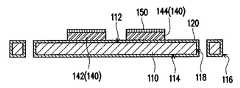
図1Eにおいて、この実施形態のパッケージ構造100aはパターン回路層140、表面保護層150、チップ160a、ボンディングワイヤー170、及び封止材180を含む。パターン回路層140はチップパッド142及びパッド144を含む。チップ160aはチップパッド142に配置され、ボンディングワイヤ170を通してパターン回路層140に電気接続する。表面保護層150はパターン回路層140に配置される。表面保護層150の一部はチップ160aとチップパッド142の間に位置する。ボンディングワイヤ170はチップ160aとパッド144上部に位置する表面保護層150を接続する。表面保護層150は、例えば、ニッケル層、金層、銀層、ニッケルパラジウム金層、又は他の適切な物質の層である。封止材180はチップ160a、ボンディングワイヤー170、表面保護層150、パターン回路層140をカプセル化し、パターン回路層140の下表面146を露出する。詳細には、パターン回路層140の下表面146及び封止材180の底面182は実質的に同一平面上にある。 In FIG. 1E, the
この実施形態のパッケージ構造100aの製造方法に基づいて、チップ160aが完全にパッケージされた後(すなわち、封止材180が形成される)、金属基板110及び金属基板110を覆うシード層120が除去される。それにより、コア誘電層を有する従来のパッケージ構造と比較すると、この発明の実施形態で述べているパッケージ構造100aは金属基板110を有さないため比較的薄い厚みを有することが出来る。除去した金属基板110は再度使用することが出来る。それに応じて、コア誘電層を有する従来のパッケージ構造の材料費と比較すると、この実施形態のパッケージ構造100aの材料費の方が下がる。その上、チップ160aはパターン回路層140に配置され、封止材180はパターン回路層140の下表面146を露出する。その結果、チップ160aによって発生された熱はパターン回路層140を通して外部環境に急速に伝送させることが出来る。その結果、この実施形態で述べているパッケージ構造100aは望ましい熱放散率を達成することが出来る。それに加え、この実施形態によると、パターン回路層の走査線の幅や厚みはパターンドライフィルム層130によって制御することが可能で、従って、必要となる精細な回路層が形成される。 Based on the manufacturing method of the
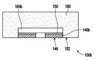
この実施形態のチップ160aは、ワイヤーボンディングによって、パッド144の上部(すなわち、パターン回路層140)に位置し、表面保護層150に電気接続しているが、チップ160aとパターン回路層140を繋げる方法はこの発明で限定しない。この発明のほかの実施形態に基づくと、図1Fに示したようにパッケージ構造100bのチップ160bは、フリップチップボンディングによって、パターン回路層140bの上部に位置する表面保護層150に電気接続している。すなわち、チップ160aとパターン回路層140を繋げる方法は、例示であって、この発明に対する限定と解釈されるべきでない。 The
パッケージ構造100c及びその製造方法は以下の実施形態に述べられる。前の実施形態で提供されたある幾つかの参照番号や記述は、以下の例示実施形態においても適応されることを言及する。同じ参照番号は同じ又は似た構成要素を示し、同じ技術内容の記述は省略する。前述の例示実施形態は省略箇所の記述の参照とすることができるので、従って、省略箇所は以下の例示実施形態で再度記述することは無い。 The
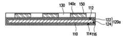
図2Aから図2Dはこの発明の他の実施形態に基づくパッケージ構造の製造方法を示す断面図である。図2Aにおいて、この実施形態のパッケージ構造の製造方法では、シード層120aが形成される金属基板110が提供される。シード層120aはシード層122及び電気めっきシード層を覆うニッケル層124から成る。シード層120aは第1表面112、第2表面114、及び金属基板110の側面116を覆う。 2A to 2D are sectional views showing a method for manufacturing a package structure according to another embodiment of the present invention. In FIG. 2A, in the manufacturing method of the package structure of this embodiment, a
図2Aで表示されたように、金属層140aはシード層120aのニッケル層124上に形成される。ここで、金属層140aはシード層120aを覆い、金属層140aの厚みはシード層120aよりも厚くなる。 As shown in FIG. 2A, the
図2Aから図2Bにおいて、パターンドライフィルム層130cは金属基板110の第1表面112に位置する金属層140aの一部に形成される。第1表面112に位置するシード層120aの一部を露出するために、エッチング遮蔽膜としてパターンドライフィルム層130cを用いて金属層140aの他の部分が除去され、パターン回路層140cが形成される。すなわち、この実施形態では、パターン回路層140cはサブトラクティブプロセスを実行することで形成される。パターンドライフィルム層130cはパターン回路層140cを露出するために除去される。 2A to 2B, the pattern dry film layer 130 c is formed on a part of the
図2Cにおいて、パターンドライフィルム層130は、第1表面112上に位置し、パターン回路層140cによって露出されたシード層120aの露出箇所に形成され、ドライフィルム層130dは第2表面114に位置するシード層120aに形成される。ドライフィルム層130dは第2表面114に位置するシード層120aを完全に覆う。表面保護層150はエッチング遮蔽膜としてパターンドライフィルム層130を用いてパターン回路層140cに電気めっきされる。 In FIG. 2C, the pattern
パターンドライフィルム層130及びドライフィルム層130dは除去され、チップボンディングプロセス(例えば、ワイヤーボンディングプロセス)は、チップ160cを表面保護層150に電気的に接続するために実行される。封止材180は金属基板110に形成され、チップ160c、表面保護層150及びパターン回路層140cをカプセル化する。金属基板110及びシード層120aは封止材180の底面182とパターン回路層140cの下表面146cを露出するために除去される。ここで、図2Dに描いたパッケージ構造100cが完全に形成される。この時、パターン回路層140cの下表面146c及び封止材180の底面182は実質的に同一平面上にある。 The pattern
この実施形態のパッケージ構造100cの製造方法によって、パッケージ160cが完全にパッケージされた後(すなわち、封止材180が形成される)、金属基板110と金属基板110を覆うシード層120aが除去される。それにより、コア誘電層を有する従来のパッケージ構造と比較すると、この発明のこの実施形態で述べたパッケージ構造100cは、金属基板110を有さないため比較的薄い厚みを有することが出来る。除去した金属基板110は再度使用することが出来る。それに応じて、コア誘電層を有する従来のパッケージ構造の材料費と比較すると、この実施形態のパッケージ構造100cの材料費の方が下がる。その上、チップ160cはパターン回路層140cに配置され、封止材180はパターン回路層140cの下表面146cを露出する。従って、チップ160cによって発生された熱はパターン回路層140cを通して外部環境に急速に伝送させることが出来る。その結果、この実施形態に述べたパッケージ構造100cは望ましい熱放散率を達成することが出来る。 According to the manufacturing method of the
要約すると、この発明の実施形態で金属基板はキャリアとして提供され、パターン回路層はめっき工程又はサブトラクティブプロセスを実行することで形成される。チップが完全にパッケージされた後、金属基板とシード層は除去される。それにより、コア誘電層を有する従来のパッケージ構造と比較すると、この発明の実施形態に記述されたパッケージ構造はキャリアを有さないため、比較的薄い厚みを有すことが出来る。その上、チップはパターン回路層に配置され、封止材はパターン回路層の下表面を露出する。従って、チップによって発生された熱は、パターン回路層を通して外部環境に急速に伝送させることが出来る。その結果、この発明の実施形態に述べたパッケージ構造は望ましい熱放散率を達成することが出来る。さらに、パターン回路層の走査線の幅や厚みはこの発明のパターンドライフィルム層によって制御することが可能で、従って、必要となる精細な回路層が形成される。 In summary, in the embodiment of the present invention, the metal substrate is provided as a carrier, and the pattern circuit layer is formed by performing a plating process or a subtractive process. After the chip is fully packaged, the metal substrate and seed layer are removed. Thereby, compared to a conventional package structure having a core dielectric layer, the package structure described in the embodiment of the present invention does not have a carrier, and therefore can have a relatively thin thickness. In addition, the chip is disposed on the pattern circuit layer, and the sealing material exposes the lower surface of the pattern circuit layer. Thus, the heat generated by the chip can be rapidly transferred to the external environment through the patterned circuit layer. As a result, the package structure described in the embodiments of the present invention can achieve a desirable heat dissipation rate. Further, the width and thickness of the scanning lines of the pattern circuit layer can be controlled by the pattern dry film layer of the present invention, and therefore a necessary fine circuit layer is formed.
以上のように、この発明を上記実施形態により開示したが、もとより、この発明を限定するためのものではなく、当業者であれば容易に理解できるように、この発明の技術思想の範囲内において、適当な変更ならびに修正が当然なされうるものであるから、その特許権保護の範囲は、特許請求の範囲および、それと均等な領域を基準として定めなければならない。 As described above, the present invention has been disclosed by the above embodiment. However, the present invention is not intended to limit the present invention and is within the scope of the technical idea of the present invention so that those skilled in the art can easily understand. Since appropriate changes and modifications can be naturally made, the scope of protection of the patent right must be determined on the basis of the scope of claims and an area equivalent thereto.
本発明は、比較的薄い厚みを有することが可能なパッケージ構造及び製造方法に関するものである。 The present invention relates to a package structure and a manufacturing method that can have a relatively small thickness.
100a、100b、100c:パッケージ構造
110:金属基板
112:第1表面
114:第2表面
116:側面
118:位置決め孔
120、120a:シード層
130、130c:パターンドライフィルム層
130d:ドライフィルム層
140、140b、140c:パターン回路層
140a:金属層
142:チップパッド
144:パッド
146、146c:下表面
150:表面保護層
160a、160b、160c:チップ
170:ボンディングワイヤー
180:封止材
182:底面100a, 100b, 100c: package structure 110: metal substrate 112: first surface 114: second surface 116: side surface 118: positioning
Claims (9)
Translated fromJapanese前記金属基板の前記第1表面に位置する前記シード層の他の部分に第1パターンドライフィルム層を形成するステップと、
前記第1パターンドライフィルム層を電気めっき遮蔽膜として用いて前記第1パターンドライフィルム層によって露出された前記シード層の一部にパターン回路層を形成した後、続いて前記パターン回路層に表面保護層を電気めっきするステップと、
前記第1パターンドライフィルム層を除去するステップと、
チップを前記表面保護層に電気的に接続するためにチップボンディングプロセスを実行するステップと、
前記金属基板に封止材を形成し、前記封止材が前記チップ、前記表面保護層、及びパターン回路層をカプセル化することと、
前記チップから発生した熱を前記表面保護層及び前記パターン回路層を通して外部環境に伝送させるために、前記金属基板及び前記シード層を除去することにより、前記封止材の底面及び前記パターン回路層の下表面を露出させるステップと、
を備え、
前記金属基板を提供するステップの後、且つ前記表面保護層を電気めっきするステップの前に、前記金属基板の前記第1表面に位置する前記シード層の一の部分に前記パターン回路層を形成するステップを更に備えるパッケージ構造の製造方法。A chemical alloy having a first surface and a second surface facing away from each other, and a side surface connecting the first surface and the second surface, wherein the first surface, the second surface, and the side surface are electroplated Providing a metal substrate covered by a seed layer that is a layer;
Forming a first pattern dry film layer on another portion of the seed layer located on the first surface of the metal substrate;
Apattern circuit layer is formed on a part of the seed layer exposed by the first pattern dry film layer using the first pattern dry film layer as an electroplating shielding film, and then surface protection is performed on the pattern circuit layer. Electroplating the layer;
Removing the first pattern dry film layer;
Performing a chip bonding process to electrically connect the chip to the surface protective layer;
Forming a sealing material on the metal substrate, and the sealing material encapsulates the chip, the surface protective layer, and the pattern circuit layer;
In order to transmit heat generated from the chip to the external environment through the surface protection layer and the pattern circuit layer, the bottom surface of the encapsulant and the pattern circuit layer are removed by removing the metal substrate and the seed layer. Exposing the lower surface ;
With
Forming the patterned circuit layer on a portion of the seed layer located on the first surface of the metal substrate after providing the metal substrate and before electroplating the surface protective layer A method for manufacturing a package structure, further comprising a step.
前記シード層に金属層を形成し、当該金属層が前記シード層を覆うここと、
前記第1表面に位置する前記金属層の一の部分に第2パターンドライフィルム層を形成することと、
前記第2パターンドライフィルム層をエッチング遮蔽膜として用いて前記金属層の他の部分を除去して、前記第1表面に位置する前記シード層の前記他の部分を露出すること、及び前記パターン回路層を形成することと、
前記第2パターンドライフィルム層を除去することと
を含む請求項1に記載のパッケージ構造の製造方法。The pattern circuit layer step comprises:
Forming a metal layer on the seed layer, the metal layer covering the seed layer; and
Forming a second pattern dry film layer on a portion of the metal layer located on the first surface;
Removing the other part of the metal layer using the second pattern dry film layer as an etching shielding film to expose the other part of the seed layer located on the first surface; and the pattern circuit Forming a layer;
The method for manufacturing a package structure according to claim 1, comprising removing the second pattern dry film layer.
前記パターン回路層に電気接続する前記チップと、
前記チップ及び前記パターン回路層をカプセル化し、前記パターン回路層の前記下表面を露出する前記封止材と
を含む請求項1に記載の製造方法を適用することによって形成されるパッケージ構造。The pattern circuit layer;
The chip electrically connected to the pattern circuit layer;
The package structure formed by applying the manufacturing method of Claim 1 which encapsulates the said chip | tip and the said pattern circuit layer, and contains the said sealing material which exposes the said lower surface of the said pattern circuit layer.
Applications Claiming Priority (2)
| Application Number | Priority Date | Filing Date | Title |
|---|---|---|---|
| TW100115473 | 2011-05-03 | ||
| TW100115473ATWI533380B (en) | 2011-05-03 | 2011-05-03 | Package structure and manufacturing method thereof |
Publications (2)
| Publication Number | Publication Date |
|---|---|
| JP2012235083A JP2012235083A (en) | 2012-11-29 |
| JP5442777B2true JP5442777B2 (en) | 2014-03-12 |
Family
ID=47089484
Family Applications (1)
| Application Number | Title | Priority Date | Filing Date |
|---|---|---|---|
| JP2012003203AExpired - Fee RelatedJP5442777B2 (en) | 2011-05-03 | 2012-01-11 | Package structure and manufacturing method thereof |
Country Status (4)
| Country | Link |
|---|---|
| US (2) | US8420951B2 (en) |
| JP (1) | JP5442777B2 (en) |
| CN (1) | CN102768960B (en) |
| TW (1) | TWI533380B (en) |
Families Citing this family (9)
| Publication number | Priority date | Publication date | Assignee | Title |
|---|---|---|---|---|
| TWI533380B (en)* | 2011-05-03 | 2016-05-11 | 旭德科技股份有限公司 | Package structure and manufacturing method thereof |
| US9892952B2 (en)* | 2014-07-25 | 2018-02-13 | Semiconductor Components Industries, Llc | Wafer level flat no-lead semiconductor packages and methods of manufacture |
| DE102015114662A1 (en)* | 2015-09-02 | 2017-03-02 | Osram Opto Semiconductors Gmbh | Method for producing an optoelectronic semiconductor component, optoelectronic semiconductor component, temporary carrier |
| CN110268510B (en) | 2016-12-22 | 2021-11-23 | 厦门四合微电子有限公司 | Packaging method of discrete device and discrete device |
| CN106783631B (en)* | 2016-12-22 | 2020-01-14 | 深圳中科四合科技有限公司 | Diode packaging method and diode |
| CN106783632B (en)* | 2016-12-22 | 2019-08-30 | 深圳中科四合科技有限公司 | A kind of packaging method of triode and triode |
| CN107146774A (en)* | 2017-04-19 | 2017-09-08 | 深圳市环基实业有限公司 | A kind of IC package support plate and its packaging technology |
| CN108807325A (en)* | 2017-05-04 | 2018-11-13 | 无锡天芯互联科技有限公司 | A kind of novel chip-packaging structure and preparation method thereof |
| CN113973431B (en)* | 2020-07-23 | 2023-08-18 | 宏启胜精密电子(秦皇岛)有限公司 | Circuit board and manufacturing method thereof |
Family Cites Families (15)
| Publication number | Priority date | Publication date | Assignee | Title |
|---|---|---|---|---|
| JPH07231062A (en)* | 1994-02-18 | 1995-08-29 | Dainippon Printing Co Ltd | Lead frame processing method |
| JP3869849B2 (en)* | 2000-04-25 | 2007-01-17 | 九州日立マクセル株式会社 | Manufacturing method of semiconductor device |
| JP4073294B2 (en)* | 2002-11-06 | 2008-04-09 | 三洋電機株式会社 | Circuit device manufacturing method |
| JP4541763B2 (en)* | 2004-01-19 | 2010-09-08 | 新光電気工業株式会社 | Circuit board manufacturing method |
| US7589407B2 (en)* | 2005-04-11 | 2009-09-15 | Stats Chippac Ltd. | Semiconductor multipackage module including tape substrate land grid array package stacked over ball grid array package |
| JP2006303305A (en)* | 2005-04-22 | 2006-11-02 | Aoi Electronics Co Ltd | Semiconductor device |
| CN100442465C (en)* | 2005-09-15 | 2008-12-10 | 南茂科技股份有限公司 | Chip packaging body process without core dielectric layer |
| JP2007109914A (en)* | 2005-10-14 | 2007-04-26 | Sony Corp | Manufacturing method of semiconductor device |
| US7875988B2 (en)* | 2007-07-31 | 2011-01-25 | Seiko Epson Corporation | Substrate and manufacturing method of the same, and semiconductor device and manufacturing method of the same |
| US7928574B2 (en)* | 2007-08-22 | 2011-04-19 | Texas Instruments Incorporated | Semiconductor package having buss-less substrate |
| TWI394248B (en)* | 2008-05-22 | 2013-04-21 | Unimicron Technology Corp | Method of manufacturing package substrate |
| TWI371830B (en)* | 2008-05-29 | 2012-09-01 | Advanced Semiconductor Eng | Circuit board process |
| US7919851B2 (en)* | 2008-06-05 | 2011-04-05 | Powertech Technology Inc. | Laminate substrate and semiconductor package utilizing the substrate |
| US8288869B2 (en)* | 2009-05-13 | 2012-10-16 | Advanced Semiconductor Engineering, Inc. | Semiconductor package with substrate having single metal layer and manufacturing methods thereof |
| TWI533380B (en)* | 2011-05-03 | 2016-05-11 | 旭德科技股份有限公司 | Package structure and manufacturing method thereof |
- 2011
- 2011-05-03TWTW100115473Apatent/TWI533380B/ennot_activeIP Right Cessation
- 2011-06-14CNCN201110158589.4Apatent/CN102768960B/ennot_activeExpired - Fee Related
- 2011-06-16USUS13/162,547patent/US8420951B2/ennot_activeExpired - Fee Related
- 2012
- 2012-01-11JPJP2012003203Apatent/JP5442777B2/ennot_activeExpired - Fee Related
- 2012-12-03USUS13/692,971patent/US8893379B2/ennot_activeExpired - Fee Related
Also Published As
| Publication number | Publication date |
|---|---|
| US20120279772A1 (en) | 2012-11-08 |
| CN102768960A (en) | 2012-11-07 |
| CN102768960B (en) | 2014-12-31 |
| US8420951B2 (en) | 2013-04-16 |
| TWI533380B (en) | 2016-05-11 |
| TW201246411A (en) | 2012-11-16 |
| JP2012235083A (en) | 2012-11-29 |
| US8893379B2 (en) | 2014-11-25 |
| US20130095615A1 (en) | 2013-04-18 |
Similar Documents
| Publication | Publication Date | Title |
|---|---|---|
| JP5442777B2 (en) | Package structure and manufacturing method thereof | |
| TWI651828B (en) | Chip package structure and method of manufacturing same | |
| JP6476231B2 (en) | Semiconductor package and manufacturing method thereof | |
| TWI435393B (en) | Package carrier board and manufacturing method thereof | |
| JP5536814B2 (en) | Package carrier manufacturing method | |
| TWI453877B (en) | Structure and process of embedded chip package | |
| JP5671504B2 (en) | Package carrier manufacturing method | |
| CN104716110B (en) | Chip packaging structure and manufacturing method thereof | |
| US7880296B2 (en) | Chip carrier structure having semiconductor chip embedded therein and metal layer formed thereon | |
| US11246223B2 (en) | Package apparatus | |
| JP2013229557A (en) | Package carrier | |
| JP5607092B2 (en) | Package structure and manufacturing method thereof | |
| CN104167369B (en) | Manufacturing method of chip packaging structure | |
| TW200933831A (en) | Integrated circuit package and the method for fabricating thereof | |
| CN104576402B (en) | Package carrier and method for manufacturing the same | |
| CN103489791A (en) | Package carrier and method for manufacturing the same | |
| JP5382889B2 (en) | Manufacturing method of package structure | |
| US12156325B2 (en) | Package carrier with improved heat dissipation efficiency and manufacturing method thereof | |
| KR20130025639A (en) | Chip package member and manufacturing method thereof | |
| TW201251547A (en) | Method for forming via holes in insulating protective layer of package substrate | |
| CN104576403A (en) | Package carrier and method for manufacturing the same |
Legal Events
| Date | Code | Title | Description |
|---|---|---|---|
| A977 | Report on retrieval | Free format text:JAPANESE INTERMEDIATE CODE: A971007 Effective date:20130416 | |
| A131 | Notification of reasons for refusal | Free format text:JAPANESE INTERMEDIATE CODE: A131 Effective date:20130423 | |
| A521 | Request for written amendment filed | Free format text:JAPANESE INTERMEDIATE CODE: A523 Effective date:20130719 | |
| A131 | Notification of reasons for refusal | Free format text:JAPANESE INTERMEDIATE CODE: A131 Effective date:20130820 | |
| A521 | Request for written amendment filed | Free format text:JAPANESE INTERMEDIATE CODE: A523 Effective date:20131029 | |
| TRDD | Decision of grant or rejection written | ||
| A01 | Written decision to grant a patent or to grant a registration (utility model) | Free format text:JAPANESE INTERMEDIATE CODE: A01 Effective date:20131119 | |
| A61 | First payment of annual fees (during grant procedure) | Free format text:JAPANESE INTERMEDIATE CODE: A61 Effective date:20131218 | |
| R150 | Certificate of patent or registration of utility model | Ref document number:5442777 Country of ref document:JP Free format text:JAPANESE INTERMEDIATE CODE: R150 Free format text:JAPANESE INTERMEDIATE CODE: R150 | |
| R250 | Receipt of annual fees | Free format text:JAPANESE INTERMEDIATE CODE: R250 | |
| R250 | Receipt of annual fees | Free format text:JAPANESE INTERMEDIATE CODE: R250 | |
| R250 | Receipt of annual fees | Free format text:JAPANESE INTERMEDIATE CODE: R250 | |
| R250 | Receipt of annual fees | Free format text:JAPANESE INTERMEDIATE CODE: R250 | |
| R250 | Receipt of annual fees | Free format text:JAPANESE INTERMEDIATE CODE: R250 | |
| R250 | Receipt of annual fees | Free format text:JAPANESE INTERMEDIATE CODE: R250 | |
| LAPS | Cancellation because of no payment of annual fees |