JP5437258B2 - Method for measuring timing characteristics of storage circuits and storage arrays (storage arrays including local clock buffers with programmable timing) - Google Patents
Method for measuring timing characteristics of storage circuits and storage arrays (storage arrays including local clock buffers with programmable timing)Download PDFInfo
- Publication number
- JP5437258B2 JP5437258B2JP2010532997AJP2010532997AJP5437258B2JP 5437258 B2JP5437258 B2JP 5437258B2JP 2010532997 AJP2010532997 AJP 2010532997AJP 2010532997 AJP2010532997 AJP 2010532997AJP 5437258 B2JP5437258 B2JP 5437258B2
- Authority
- JP
- Japan
- Prior art keywords
- clock signal
- local clock
- control value
- read
- circuit
- Prior art date
- Legal status (The legal status is an assumption and is not a legal conclusion. Google has not performed a legal analysis and makes no representation as to the accuracy of the status listed.)
- Expired - Fee Related
Links
- 238000003860storageMethods0.000titleclaimsdescription60
- 238000000034methodMethods0.000titleclaimsdescription31
- 239000000872bufferSubstances0.000titledescription10
- 238000003491arrayMethods0.000titledescription6
- 230000003111delayed effectEffects0.000claimsdescription35
- 210000000352storage cellAnatomy0.000claimsdescription26
- 238000011156evaluationMethods0.000claimsdescription21
- 210000004027cellAnatomy0.000claimsdescription17
- 230000004044responseEffects0.000claimsdescription17
- 230000003213activating effectEffects0.000claimsdescription3
- 238000005259measurementMethods0.000description25
- 238000012360testing methodMethods0.000description22
- 235000012431wafersNutrition0.000description16
- 238000010586diagramMethods0.000description9
- 238000004519manufacturing processMethods0.000description8
- 239000000523sampleSubstances0.000description8
- 238000013461designMethods0.000description5
- 230000008859changeEffects0.000description4
- 230000000295complement effectEffects0.000description4
- 230000000630rising effectEffects0.000description4
- 230000003068static effectEffects0.000description4
- HCUOEKSZWPGJIM-YBRHCDHNSA-N(e,2e)-2-hydroxyimino-6-methoxy-4-methyl-5-nitrohex-3-enamideChemical compoundCOCC([N+]([O-])=O)\C(C)=C\C(=N/O)\C(N)=OHCUOEKSZWPGJIM-YBRHCDHNSA-N0.000description3
- 101001109689Homo sapiens Nuclear receptor subfamily 4 group A member 3Proteins0.000description3
- 101000598778Homo sapiens Protein OSCP1Proteins0.000description3
- 101001067395Mus musculus Phospholipid scramblase 1Proteins0.000description3
- 102100022673Nuclear receptor subfamily 4 group A member 3Human genes0.000description3
- 230000007423decreaseEffects0.000description3
- 230000008569processEffects0.000description3
- 230000001934delayEffects0.000description2
- 230000007246mechanismEffects0.000description2
- 230000003287optical effectEffects0.000description2
- 238000004088simulationMethods0.000description2
- 102220496565MAGUK p55 subfamily member 3_I21A_mutationHuman genes0.000description1
- 102220625795Sulfotransferase 2B1_I20A_mutationHuman genes0.000description1
- 230000002776aggregationEffects0.000description1
- 238000004220aggregationMethods0.000description1
- 238000004458analytical methodMethods0.000description1
- 230000015572biosynthetic processEffects0.000description1
- 238000013075data extractionMethods0.000description1
- 230000003247decreasing effectEffects0.000description1
- 238000009826distributionMethods0.000description1
- 238000005516engineering processMethods0.000description1
- 230000006870functionEffects0.000description1
- 230000001939inductive effectEffects0.000description1
- 238000002360preparation methodMethods0.000description1
- 238000012545processingMethods0.000description1
- 102200132943rs199473363Human genes0.000description1
- 238000000638solvent extractionMethods0.000description1
- 230000000638stimulationEffects0.000description1
- 230000001960triggered effectEffects0.000description1
- 238000003079width controlMethods0.000description1
Images


Classifications
- G—PHYSICS
- G11—INFORMATION STORAGE
- G11C—STATIC STORES
- G11C7/00—Arrangements for writing information into, or reading information out from, a digital store
- G11C7/22—Read-write [R-W] timing or clocking circuits; Read-write [R-W] control signal generators or management
- G—PHYSICS
- G11—INFORMATION STORAGE
- G11C—STATIC STORES
- G11C11/00—Digital stores characterised by the use of particular electric or magnetic storage elements; Storage elements therefor
- G11C11/21—Digital stores characterised by the use of particular electric or magnetic storage elements; Storage elements therefor using electric elements
- G11C11/34—Digital stores characterised by the use of particular electric or magnetic storage elements; Storage elements therefor using electric elements using semiconductor devices
- G11C11/40—Digital stores characterised by the use of particular electric or magnetic storage elements; Storage elements therefor using electric elements using semiconductor devices using transistors
- G11C11/41—Digital stores characterised by the use of particular electric or magnetic storage elements; Storage elements therefor using electric elements using semiconductor devices using transistors forming static cells with positive feedback, i.e. cells not needing refreshing or charge regeneration, e.g. bistable multivibrator or Schmitt trigger
- G11C11/413—Auxiliary circuits, e.g. for addressing, decoding, driving, writing, sensing, timing or power reduction
- G—PHYSICS
- G11—INFORMATION STORAGE
- G11C—STATIC STORES
- G11C29/00—Checking stores for correct operation ; Subsequent repair; Testing stores during standby or offline operation
- G11C29/02—Detection or location of defective auxiliary circuits, e.g. defective refresh counters
- G—PHYSICS
- G11—INFORMATION STORAGE
- G11C—STATIC STORES
- G11C29/00—Checking stores for correct operation ; Subsequent repair; Testing stores during standby or offline operation
- G11C29/02—Detection or location of defective auxiliary circuits, e.g. defective refresh counters
- G11C29/023—Detection or location of defective auxiliary circuits, e.g. defective refresh counters in clock generator or timing circuitry
- G—PHYSICS
- G11—INFORMATION STORAGE
- G11C—STATIC STORES
- G11C29/00—Checking stores for correct operation ; Subsequent repair; Testing stores during standby or offline operation
- G11C29/04—Detection or location of defective memory elements, e.g. cell constructio details, timing of test signals
- G11C29/08—Functional testing, e.g. testing during refresh, power-on self testing [POST] or distributed testing
- G11C29/12—Built-in arrangements for testing, e.g. built-in self testing [BIST] or interconnection details
- G11C29/14—Implementation of control logic, e.g. test mode decoders
- G—PHYSICS
- G11—INFORMATION STORAGE
- G11C—STATIC STORES
- G11C29/00—Checking stores for correct operation ; Subsequent repair; Testing stores during standby or offline operation
- G11C29/04—Detection or location of defective memory elements, e.g. cell constructio details, timing of test signals
- G11C29/50—Marginal testing, e.g. race, voltage or current testing
- G11C29/50012—Marginal testing, e.g. race, voltage or current testing of timing
- G—PHYSICS
- G11—INFORMATION STORAGE
- G11C—STATIC STORES
- G11C7/00—Arrangements for writing information into, or reading information out from, a digital store
- G11C7/10—Input/output [I/O] data interface arrangements, e.g. I/O data control circuits, I/O data buffers
- G11C7/1051—Data output circuits, e.g. read-out amplifiers, data output buffers, data output registers, data output level conversion circuits
- G11C7/1069—I/O lines read out arrangements
- G—PHYSICS
- G11—INFORMATION STORAGE
- G11C—STATIC STORES
- G11C7/00—Arrangements for writing information into, or reading information out from, a digital store
- G11C7/12—Bit line control circuits, e.g. drivers, boosters, pull-up circuits, pull-down circuits, precharging circuits, equalising circuits, for bit lines
- G—PHYSICS
- G11—INFORMATION STORAGE
- G11C—STATIC STORES
- G11C7/00—Arrangements for writing information into, or reading information out from, a digital store
- G11C7/22—Read-write [R-W] timing or clocking circuits; Read-write [R-W] control signal generators or management
- G11C7/222—Clock generating, synchronizing or distributing circuits within memory device
- G—PHYSICS
- G11—INFORMATION STORAGE
- G11C—STATIC STORES
- G11C8/00—Arrangements for selecting an address in a digital store
- G11C8/08—Word line control circuits, e.g. drivers, boosters, pull-up circuits, pull-down circuits, precharging circuits, for word lines
Landscapes
- Engineering & Computer Science (AREA)
- Microelectronics & Electronic Packaging (AREA)
- Computer Hardware Design (AREA)
- Tests Of Electronic Circuits (AREA)
- Test And Diagnosis Of Digital Computers (AREA)
- Static Random-Access Memory (AREA)
Description
Translated fromJapanese本発明は、一般に、メモリ回路に関し、詳細には、アレイの内部タイミング・マージン(timing margin)を決定するために調整可能なタイミングを有するローカル・クロック・バッファを備えたストレージ・アレイ(storage array)に関する。 The present invention relates generally to memory circuits and, in particular, a storage array with a local clock buffer having adjustable timing to determine the internal timing margin of the array. About.
記憶セルのパフォーマンスは、現在の処理システムにおいて重大な制限事項であり、技術が進歩するにつれて重大な制限事項以上のものになると予測されている。特に、スタティック・ランダム・アクセス・メモリ(SRAM)セルは、データおよびプログラム命令への高速アクセスを可能にするためにプロセッサ・キャッシュおよび外部記憶域で使用される。また、スタティック記憶セルは、内部に、たとえば、プロセッサ・レジスタに値を保管するために、プロセッサおよびその他のデジタル回路内でも使用される。プロセッサ・サイクル周波数が4GHzよりかなり上に達している場合、その期間内に値を保管し、保管された値へのアクセスを可能にすることができるSRAMセルの開発が必要になっている。しかし、記憶セル・アクセス時間が減少するにつれて、読み取りおよび書き込み両方のアクセス・サイクルの様々な部分の内部タイミング・マージンを決定することは難題を提示するものである。プローブを使用して、読み取りまたは書き込み操作の内部タイミングを測定しようと試みる場合、そのプローブはセルのタイミングを変更し、誤った結果をもたらす。Storage cell performance is a significant limitation in current processing systems and is expected to become more than a critical limitation as technology advances. In particular, static random access memory (SRAM) cells are used in processor caches and external storage to allow fast access to data and program instructions. Static storage cells are also used internally, for example in processors and other digital circuits, to store values in processor registers. If the processor cycle frequency reaches well above 4G Hz, store the values within that period, it has become necessary to develop a SRAM cell that can enable access to the stored value . However, as storage cell access times decrease, determining internal timing margins for various parts of both read and write access cycles presents challenges. If a probe is used to attempt to measure the internal timing of a read or write operation, the probe will change the timing of the cell with incorrect results.
記憶セルのアクセス時間が減少するにつれて、回路シミュレーションの妥当性も減少し、したがって、シミュレーションは貴重であるが、その完全実装状態になっている実際の記憶装置、たとえば、ストレージ・アレイおよびアクセス回路全体で実行される測定は必要不可欠なものである。タイミング・マージンは、ストレージ・アレイ設計を含むコンポーネントの潜在的に指定されたかまたは要求されたパフォーマンスと生産歩留まりとの関係を示すので、ストレージ・アレイ設計の潜在的パフォーマンスを示す直接的標識である。さらに、ダイ同士の間および1つのダイ内のタイミング・マージンの変動により、プロセス変動および特定の障害メカニズムに関する情報が明らかになる。 As the access time of a storage cell decreases, the validity of the circuit simulation also decreases, so the simulation is valuable but the actual storage device in its fully implemented state, for example, the entire storage array and access circuit Measurements carried out in are essential. Timing margin is a direct indicator of the potential performance of a storage array design because it shows the relationship between the potential specified or required performance of a component that includes the storage array design and production yield. In addition, timing margin variations between dies and within one die reveal information about process variations and specific failure mechanisms.
記憶セルの内部タイミングの各部分でデータを得るために、ワンショット遅延線(one-shot delay line)およびリング発振器(ringoscillator)などの様々な技法が使用されてきた。しかし、このような回路によって行われる測定に基づくタイミング・マージンの完全なモデルは、一般に、全体的なタイミング・マージンを得るために個々のタイミング部分測定機能を含む複数のテスト回路からの測定値の合計を含まなければならない。完全なタイミング・マージンを実装するために必要な遅延またはリング発振器あるいはその両方のテスト回路のすべてを含むことは、相当な回路面積を消費する可能性があり、テスト回路を取り入れた装置のレイアウトの変更が必要になる可能性もある。さらに、一般に、このような測定に関連するプロービング要件が存在し、生産回路で実用的ではない可能性があるテスト・パッドが必要になるか、またはそのテスト・パッドを提供するためにレイアウトの大幅な分裂が必要になるであろう。最後に、リング発振器および遅延線回路内の記憶セル・パフォーマンスの集約であるため、このような技法は典型的に、個々の記憶セルのパフォーマンスを測定するわけではない。アレイの全域でデバイス特性が変動するため、ならびに、アレイ内の様々な位置で最悪の信号タイミング条件があるために、アレイ内のそれぞれのセルのパフォーマンスを測定することが望ましい。 Various techniques such as one-shot delay lines and ringoscillators have been used to obtain data at each part of the internal timing of the storage cell. However, complete models of timing margins based on the measurements made by such circuits generally do not provide measurements from multiple test circuits that include individual timing portion measurement functions to obtain an overall timing margin. Must include the total. Including all of the delay and / or ring oscillator test circuits necessary to implement a complete timing margin can consume considerable circuit area and can be used in the layout of a device incorporating the test circuit. Changes may be required. In addition, there are generally probing requirements associated with such measurements that require a test pad that may not be practical in production circuits, or a significant increase in layout to provide that test pad. Split will be necessary. Finally, such techniques typically do not measure the performance of individual storage cells because of the aggregation of storage cell performance within the ring oscillator and delay line circuitry. It is desirable to measure the performance of each cell in the array because of variations in device characteristics across the array, and because of the worst signal timing requirements at various locations within the array.
したがって、実際のストレージ・アレイの動作条件下で、個々のセルを含む記憶セルの内部タイミング・マージンを正確に決定するためのテスト回路および方法を提供することが望ましい。さらに、テスト回路を生産ストレージ・アレイに容易に取り入れることができ、アレイおよびアクセス回路設計を大幅に混乱させないように、小さい回路面積のみを必要とするようなテスト回路を提供することが望ましい。 Accordingly, it would be desirable to provide a test circuit and method for accurately determining the internal timing margin of storage cells, including individual cells, under actual storage array operating conditions. In addition, it is desirable to provide a test circuit that can be easily incorporated into a production storage array and requires only a small circuit area so as not to significantly disrupt the array and access circuit design.
個々の記憶セルのタイミング・マージンを含む、ストレージ・アレイ内の内部タイミング・マージンを正確に決定するという目的は、実装のために小さい追加の回路面積のみを必要とするローカル・クロック・バッファ回路を含むストレージ・アレイで達成される。ローカル・クロック・バッファ回路は、テスト・ストレージ・アレイまたは生産ストレージ・アレイあるいはその両方内に統合することができる。また、ストレージ・アレイは、調整可能なタイミングを備えた汎用ストレージ・アレイとして使用することもできる。 The purpose of accurately determining the internal timing margin in the storage array, including the timing margin of individual storage cells, is to reduce the local clock buffer circuit that requires only a small additional circuit area for implementation. Achieved with a storage array containing. The local clock buffer circuit can be integrated into the test storage array, the production storage array, or both. The storage array can also be used as a general purpose storage array with adjustable timing.
この回路は、ローカル・ワード線、グローバル・ビット線、およびローカル/グローバル・プレチャージ・タイミングに関する遅延時間およびパルス幅について、プログラマブルまたはその他の外部誘導調整を可能にする。ローカル・ワード線信号とグローバル・ビット線読み取り回路イネーブルとの間の遅延ならびにワード線および読み取りイネーブル信号のパルス幅を調整するアナログ・バイアスまたは選択回路を制御するデジタル値をラッチにロードする。代わって、遅延デバイスを制御するためにテスト・ポイント/端子を介してアナログ電圧を導入することができる。遅延およびパルス幅制御によって設定された実際の遅延およびパルス幅を収集するためにパルス幅測定回路をストレージ・アレイ内に含めることができる。 This circuit allows programmable or other external inductive adjustments for delay times and pulse widths for local word lines, global bit lines, and local / global precharge timing. The latch is loaded with a digital value that controls the analog bias or selection circuit that adjusts the delay between the local word line signal and the global bit line read circuit enable and the pulse width of the word line and read enable signal. Alternatively, an analog voltage can be introduced through the test point / terminal to control the delay device. A pulse width measurement circuit can be included in the storage array to collect the actual delay and pulse width set by the delay and pulse width control.
特定のストレージ・アレイおよびストレージ・アレイ動作条件、たとえば、温度および電源電圧に関する動作可能範囲を決定するために、ワード線およびグローバル・ビット線読み取りイネーブル信号のパルス幅ならびにワード線とグローバル・ビット線との読み取りイネーブル信号遅延を変化させ、測定する。ストレージ・アレイに関する信号タイミング・マージンを決定するために、パルス幅ならびにワード線とグローバル・ビット線との読み取りイネーブル信号遅延のそれぞれについて障害ポイントを決定することにより、タイミング・マージンを抽出する。 To determine the operational range for specific storage arrays and storage array operating conditions, such as temperature and supply voltage, the pulse width of the word line and global bit line read enable signals and the word lines and global bit lines The read enable signal delay is varied and measured. To determine the signal timing margin for the storage array, the timing margin is extracted by determining the failure point for each of the pulse width and the read enable signal delay for the word lines and global bit lines.
本発明の上記その他の目的、特徴、および利点は、添付図面に示されているように、以下に示す本発明の好ましい実施形態の詳細な説明から明らかになるであろう。 These and other objects, features and advantages of the present invention will become apparent from the following detailed description of the preferred embodiments of the invention as illustrated in the accompanying drawings.
本発明に特有と思われる新規な特徴は、特許請求の範囲に明記されている。しかし、本発明そのもの、ならびにその好ましい使用態様、追加の目的、および利点については、同様の参照番号が同様のコンポーネントを示す添付図面に併せて読んだときに、例示的な一実施形態に関する以下の詳細な説明を参照することによって最も良く理解されるであろう。 The novel features believed characteristic of the invention are set forth in the appended claims. However, the present invention itself, as well as its preferred modes of use, additional objects and advantages, will be described below with respect to an exemplary embodiment, when read in conjunction with the accompanying drawings, wherein like reference numerals indicate like components. It will be best understood by reference to the detailed description.
本発明は、動作およびマージンの設計改良と決定を容易にするために、記憶セル、たとえば、レジスタまたはスタティック・メモリ・セルにアクセスするためのタイミング・マージンを評価するためのストレージ・アレイ回路に関する。ストレージ・アレイは、調整可能なタイミングを備えた汎用アレイとしても使用することができる。ワード線アサート・タイミングおよびパルス幅ならびにグローバル・ビット線評価タイミングおよびパルス線を制御することによりセルへのアクセスのタイミングをとるローカル・クロック・バッファ内にプログラマブル遅延が設けられている。セル、ビット線、および読み取りセンス回路/書き込み回路の回路ローディングおよび構造は、生産ストレージ・アレイ内のものと同一であり、生産アレイ実装例における正確な測定タイミング・マージンをもたらし、本発明の回路は一時的にまたは永続的に生産ストレージ・アレイ内に取り入れることができる。 The present invention relates to a storage array circuit for evaluating timing margins for accessing storage cells, eg, registers or static memory cells, to facilitate operational and margin design improvements and determinations. The storage array can also be used as a general purpose array with adjustable timing. A programmable delay is provided in the local clock buffer that times the access to the cell by controlling the word line assert timing and pulse width and the global bit line evaluation timing and pulse line. The circuit loading and structure of the cells, bit lines, and read sense / write circuits are the same as in a production storage array, resulting in accurate measurement timing margins in production array implementations, and the circuit of the present invention is Can be temporarily or permanently incorporated into a production storage array.
次に、図面に関連して、特に図1に関連して説明すると、本発明の一実施形態によるストレージ・サブアレイ回路のブロック図が示されている。行および列を形成する記憶セル10のサブアレイは読み取り/書き込みアクセス回路に接続されている。読み取り/書き込みアクセス回路は、ワード線制御信号wl[0:N]に応じて行内のセル10を活動化するワード線選択ロジック14と、サブアレイ・ローカル・ビット線lblc[0:M]、lblt[0:M]をゲートしてグローバル・ビット線gbl上の結果の値を評価し、結果の値をラッチする読み取りラッチ/ビット線評価回路16とを含む。ビット線プレチャージ回路12は、記憶セル10の読み取りアクセスの準備としてローカル・ビット線lblc[0:M]、lblt[0:M]をプレチャージし、記憶セル10の書き込みアクセス中に書き込みロジックから提供された入力値に応じてそれぞれの値を設定する。Referring now to the drawings, and more particularly to FIG. 1, a block diagram of a storage subarray circuit according to one embodiment of the present invention is shown. The subarrays of
ローカル・クロック・バッファ18は、グローバル・クロック信号Global clkから導出されるローカル・クロック信号lclkおよび遅延クロック信号dellclkを含むローカル制御信号を提供する。ローカル・クロック信号lclkは、ワード線選択ロジック14を介してワード線制御信号wl[0:N]のタイミングを制御し、このワード線制御信号は記憶セル10内のパス・デバイスを活動化して、読み取りまたは書き込み操作を実行するためにその内部記憶素子をローカル・ビット線lblc[0:M]、lblt[0:M]に結合する。また、ローカル・クロック信号lclkは、ローカル・ビット線lblc[0:M]、lblt[0:M]の書き込みセットアップおよびプレチャージ・タイミングも制御し、そのタイミングは一般に、ワード線タイミングに対する相補期間(complementary timeperiod)として生成される。遅延クロック信号dellclkは、読み取り操作中に記憶セル10によってローカル・ビット線lblc[0:M]、lblt[0:M]に課された値の評価のタイミングならびに評価の結果のラッチのタイミングを制御する。The
本発明では、ローカル・クロック・バッファ18は1つまたは複数のadjust信号によって提供されたプログラマブル・タイミングを有し、そのadjust信号は、ローカル・クロック信号lclkおよび遅延クロック信号dellclkのパルス幅と、ローカル・クロック信号lclkおよび遅延クロック信号dellclkの立ち上がり間の遅延時間のうちの1つまたは複数を独立して設定するアナログまたはデジタル制御信号である。図1のストレージ・アレイ回路は、adjust信号を介してプログラミングされた遅延およびパルス幅の値を外部クロック信号ext clkを基準として測定することができ、アレイのタイミング・マージンを評価するときにadjust信号によって設定された正確な遅延およびパルス幅の安定し反復可能な測定値を決定できるように、パルス幅/遅延検出器回路20も含む。1組のデジタル信号measure outは、パルス幅/遅延検出器回路20によって測定されたパルス幅および遅延時間の指示に対してスキャン可能なアクセスを可能にする。In the present invention,
図1に描写されている例示的な実施形態は特にダイナミック・ロジック評価回路およびローカル/グローバル・ビット線パーティション化を有するスタティック・ストレージ・アレイを対象とするが、本発明の技法は、アレイ内部の制御信号のパルス幅(複数も可)および相対タイミングを調整することによりタイミング・マージンを評価することができる他のタイプのストレージ・アレイに適用されることは言うまでもない。本明細書に記載されている方法および回路技法は、図1に示されているものなどのストレージ・アレイならびに他のタイプのストレージ・アレイおよび一般のダイナミック・ロジック回路に適用可能である。 Although the exemplary embodiment depicted in FIG. 1 is specifically directed to a static storage array with dynamic logic evaluation circuitry and local / global bit line partitioning, the techniques of the present invention are internal to the array. It goes without saying that it applies to other types of storage arrays where the timing margin can be evaluated by adjusting the pulse width (s) and relative timing of the control signal. The methods and circuit techniques described herein are applicable to storage arrays such as that shown in FIG. 1 as well as other types of storage arrays and general dynamic logic circuits.
次に、図2を参照すると、本発明の一実施形態によるローカル・クロック・バッファ18の詳細が示されている。enable pulse mode信号は遅延線DL1〜DL3を活動化し、その遅延線は本発明のプログラマブル/調整可能制御信号タイミングを提供する。enable pulse mode信号がアサート解除されると、回路のタイミングはデフォルトとして使用可能な最高速タイミングになり、したがって、図1に描写されているサブアレイを生産アレイ・モードで操作するのに適している。enable pulse mode信号がアサートされると、adjust信号を介してローカル・クロック信号lclkおよび遅延クロック信号dellclkのタイミングを調整することができる。遅延回路DL1は、論理NORゲートNOR1の一方の入力に印加されるグローバル・クロック信号gclkを遅延させる。論理NORゲートNOR1のもう一方の入力はグローバル・クロック信号gclkに直接接続され、その結果、遅延回路DL1は論理NORゲートNOR1の出力で提供されるアクティブロー・パルス信号に対してグローバル・クロック信号gclkの立ち下がりを遅延させ、したがって、遅延回路DL1によって提供される遅延時間長に応じてパルスの幅を引き延ばす。論理NANDゲートNAND1は、subarray decode信号でアクティブロー・パルスを修飾し、ローカル・クロック信号lclkを生成するためにインバータI1によって反転された他のアクティブロー・パルスを論理NANDゲートNAND1の出力で生成する。また、論理NANDゲートNAND1の出力は、遅延回路DL2の遅延時間によって決定された遅延を有する論理NANDゲートNAND2の第2の入力の遅延バージョンとともに、論理NANDゲートNAND2の第1の入力に直接提供される。論理NANDゲートNAND1のアクティブロー・パルス出力は、論理NANDゲートNAND2の出力でアクティブハイ・パルスを生成し、立ち下がりは遅延回路DL2の遅延時間によって調整されている。遅延回路DL3は遅延クロック信号dellclkの遅延全体を調整し、その信号は遅延回路DL3の出力からインバータI2〜I3によってバッファされる。 Referring now to FIG. 2, details of the
次に、図3を参照すると、記憶セル読み取りサイクルに関する図1および図2の回路内の信号タイミングが示されている。グローバル・クロック信号Global clkのアサート前に、ローカル・ビット線lblc[0:M]、lblt[0:M]はそれぞれのプレチャージ状態になっている。グローバル・クロック信号Global clkがアサートされると(アクティブロー)、ローカル・クロック信号lclkは時間T1でアサートし(アクティブハイ)、ワード線信号wlを活動化し、それにより選択された記憶セル10内のパス・ゲートを活動化する。次にローカル・ビット線lblc[0:M]、lblt[0:M]は評価を行う(立ち下がり信号lbltによって示されている)。図2の遅延回路DL3によって提供される遅延時間dl3により調整可能な時間T2で、遅延クロック信号dellclkがアサートされ(アクティブハイ)、それにより図1の読み取りラッチ/ビット線評価回路16内の評価回路上にローカル・ビット線lblc[0:M]、lblt[0:M]をゲートする。その結果として、グローバル・ビット線gblは評価を行う(ロー)。図2の遅延回路DL1によって提供される遅延時間dl1により調整可能な時間T3で、ローカル・クロック信号lclkがアサート解除され、ローカル・ビット線lblc[0:M]、lblt[0:M]はローカル・クロック信号lclkの立ち下がりによって図1のビット線プレチャージ回路12の活動化によりそれぞれのプレチャージ状態に戻る。最後に、時間T4で、図2の遅延回路DL2によって提供される遅延時間dl2により調整可能な遅延クロック信号dellclkの立ち下がりにより、図1の読み取りラッチ/ビット線評価回路16内の読み取りラッチは図1の記憶セル10から読み取られた値を収集し、データ信号doutを産出する。Referring now to FIG. 3, signal timing within the circuits of FIGS. 1 and 2 for a memory cell read cycle is shown. Before asserting the global clock signal Global clk, the local bit linelbl c [0: M], lblt [0: M] is in the respective precharge state. When the global clock signal Global clk is asserted (active low), the local clock signal lclk asserts at time T1 (active high), activating the word line signal wl, thereby causing the selected
したがって、上記の例証では、ローカル・クロック・バッファ18は、ストレージ・アレイに関する制御信号によって生成されたすべてのクリティカル・タイミングのイベントの調整を行う。図1の読み取りラッチ/ビット線評価回路16内の評価回路に対するローカル・ビット線lblc[0:M]、lblt[0:M]の不適切なセットアップのためにdout値にエラーが現れるまで遅延時間dl1を短縮するかまたは遅延時間dl3を増加するかあるいはその両方を行うことによってローカル・クロック信号lclkの幅を縮小することにより、最小ローカル・ビット線アクセス時間を決定することができる。同様に、エラーが現れるまで遅延時間dl2を減少することにより、最小評価/読み取りラッチ・セットアップ時間を決定することができる。アレイ内の特定の記憶セル10でまたはアレイ内のそれぞれの記憶セル10についてタイミング・マージンを決定することにより、ストレージ・アレイ内の特定の位置の最悪タイミングならびにアレイ全体のランダム・タイミング変動について検討することができる。また、遅延時間dl1の調整によりワード線信号wlの最小幅の調整が可能であり、それによりローカル・ビット線lblc[0:M]、lblt[0:M]からの値の記憶セル10への書き込みを制御するので、本発明により、書き込みサイクル・タイミング・マージンも決定することができる。Thus, in the above example, the
次に、図4を参照すると、図2の遅延回路DL1〜DL3を実装するために使用可能な遅延素子が示されている。トランジスタN1およびP1は、バイアス電圧Vbiasによって設定されたバイアス・レベルを有するトランジスタN2によって設定された電流レベルを有するインバータを形成する。バイアス電圧Vbiasを低減すると、トランジスタN1およびP1によって形成されたインバータを「枯渇(starve)」させ、スイッチング時間を増加し、それにより回路の遅延を増加する。バイアス電圧Vbiasは、図1のストレージ・アレイ回路が集積されているダイのテスト・ポイント(図2の遅延回路DL1〜DL3に供給される各バイアス電圧用のテスト・ポイントを含む)から提供される場合もあれば、バイアス電圧がデジタル制御値からローカルで生成される場合もある。したがって、図1および図2に示されているadjust信号(複数も可)は、遅延回路DL1〜DL3のそれぞれに1つまたは複数のバイアス電圧(複数も可)Vbiasを供給するアナログ信号(複数も可)である場合もあれば、adjust信号(複数も可)は、たとえば、図1のストレージ・アレイ回路が集積されているダイ上に集積されたスキャン・ラッチから提供されるデジタル信号である場合もある。パッケージ化されたダイまたはパッケージ化されていないダイ上に集積されたテスト回路にローカルのアナログまたはデジタル制御信号を提供するために多くの技法が存在することは言うまでもなく、これを使用して、本発明のタイミング・マージン分析を実行するように遅延回路DL1〜DL3を制御することができる。 Next, FIG. 4 shows a delay element that can be used to implement the delay circuits DL1 to DL3 of FIG. Transistors N1 and P1 form an inverter having a current level set by transistor N2 having a bias level set by bias voltage Vbias. Decreasing the bias voltage Vbias “starves” the inverter formed by transistors N1 and P1, increasing the switching time and thereby increasing the circuit delay. The bias voltage Vbias is provided from a test point (including a test point for each bias voltage supplied to the delay circuits DL1 to DL3 in FIG. 2) of the die in which the storage array circuit in FIG. 1 is integrated. In some cases, the bias voltage may be generated locally from the digital control value. Accordingly, the adjust signal (s) shown in FIGS. 1 and 2 is the analog signal (s) that supplies one or more bias voltage (s) Vbias to each of the delay circuits DL1-DL3. Or the adjust signal (s) may be, for example, a digital signal provided from a scan latch integrated on the die on which the storage array circuit of FIG. 1 is integrated. There is also. It goes without saying that there are many techniques for providing local analog or digital control signals to test circuits integrated on packaged or unpackaged dies. Delay circuits DL1-DL3 can be controlled to perform the timing margin analysis of the invention.
図5は、上述のスキャン・レジスタまたはその他のデジタル値供給手段から供給可能なデジタル制御値<c0:c7>からバイアス電圧Vbiasをローカルで生成するためのバイアス生成回路を示している。トランジスタN3およびN4はトランジスタN6およびトランジスタN10B〜N17Bにバイアス電圧値を供給し、それらのトランジスタはトランジスタP2を通って引き出される電流レベルを設定し、それがトランジスタP3によってミラーリングされる。トランジスタN7はフォロワ(follower)を提供し、トランジスタN8は、デジタル制御値<c0:c7>によってトランジスタP2によりプログラミングされる電流レベルによって電圧Vbiasが設定されるようなインピーダンスを提供する。したがって、図4および図5の回路の組み合わせにより、スキャン・ラッチまたは他のデジタル・インターフェースから提供される値に応答して、図2の遅延回路DL1〜DL3の遅延を変更するために使用できるデジタル制御の遅延回路が提供される。 FIG. 5 shows a bias generation circuit for locally generating the bias voltage Vbias from the digital control values <c0: c7> that can be supplied from the above-described scan register or other digital value supply means. Transistors N3 and N4 supply bias voltage values to transistor N6 and transistors N10B-N17B, which set the current level drawn through transistor P2, which is mirrored by transistor P3. Transistor N7 provides a follower and transistor N8 provides an impedance such that the voltage Vbias is set by the current level programmed by transistor P2 with the digital control value <c0: c7>. Thus, the combination of the circuits of FIGS. 4 and 5 can be used to change the delay of the delay circuits DL1-DL3 of FIG. 2 in response to a value provided from a scan latch or other digital interface. A control delay circuit is provided.
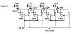
次に、図6を参照すると、本発明の一実施形態によりパルス幅/遅延検出器20の詳細が示されている。上述の通り、遅延回路DL1〜DL3内のもの以外のコンポーネントは変化するので、遅延回路DL1〜DL3の遅延を変更するだけでなく、導入される遅延の正確な測定値を有することも望ましい。また、トランジスタP1およびN1〜N2のサイズの変化によって特定のバイアス電圧Vbiasに対する時間遅延の変化が引き起こされるので、遅延回路DL1〜DL3内の変動は図4のような諸実施形態に存在することになる。したがって、パルス幅/遅延検出器20は、ローカル・クロック信号lclkおよび遅延クロック信号dellclkのパルス幅ならびにローカル・クロック信号lclkのエッジと遅延クロック信号dellclkのエッジとの遅延を測定するためのメカニズムを提供する。論理NANDゲートNAND10〜NAND12は、スキャン・ラッチまたは他のデジタル・インターフェースを介して提供可能な選択信号sellclkおよびseldellclkに応答してローカル・クロック信号lclkと遅延クロック信号dellclkとを選択するセレクタを形成する。論理NANDゲートNAND12の出力は、1対のインバータ・チェーンに提供される。第1のチェーンはインバータI10、I11、およびI13により反転信号経路を提供し、信号経路間の遅延のバランスを取り、Nチャネル対Pチャネルのデバイス・スキューによる立ち上がりと立ち下がりに関するスキュー時間の相違を補償するためにダミー・ローディング・インバータI12が接続されている。第2のインバータ・チェーンは、インバータI14〜I17を含み、非反転信号経路を提供する。論理NANDゲートNAND13〜NAND15によって形成されるもう1つのセレクタは、スキャン・ラッチまたは他のデジタル入力手段から提供される選択信号invertおよび/invertに応答して非反転信号経路出力と反転信号経路出力とを選択する。したがって、論理NANDゲートNAND15の出力は、ローカル・クロック信号lclkのいずれかの極性または遅延クロック信号dellclkのいずれかの極性から選択される。 Referring now to FIG. 6, details of the pulse width /
図6のパルス幅/遅延検出器回路20における遅延/パルス幅測定は、外部供給の安定した基準クロックext clkの位相に対して論理NANDゲートNAND15の出力で選択されたクロック信号のエッジの位置を決定することによって実行される。インバータI20A、I21A、・・・I20N、I21Nによって形成されたインバータ・チェーンは、測定対象の選択されたクロック信号の遅延バージョンをインバータI22A〜I22Nを介して1組のラッチQ1〜QNの入力に提供する。ラッチQ1〜QNは外部クロック信号ext clkによってクロック制御され、ラッチQ1〜QNの出力は測定結果としてスキャン・ラッチまたは他のデジタル出力インターフェースを介してテスト・システムに提供される。ローカル・クロック信号lclkまたは遅延クロック信号dellclkのいずれかのパルス幅は、測定対象の選択されたクロック信号の立ち上がりがラッチQ1〜QNのうちの特定のラッチに現れる論理「1」によって検出されるまで外部クロック信号ext clkの位相を調整することによって実行される。次に外部クロック信号ext clkの位相は、論理「0」がラッチQ1〜QNのうちの同じ特定のラッチに現れるまで調整される。外部クロック信号ext clkの位相は両方のエッジ検出時に収集され、測定された位相の差によって測定対象の選択されたクロックのパルス幅が得られる。ローカル・クロック信号lclkと遅延クロック信号dellclkとの遅延を決定するために、ローカル・クロック信号lclkの立ち上がりおよび遅延クロック信号dellclkの立ち上がりに関して同じ手順に従うことができる。それぞれの測定は複数回(一般に数百回)繰り返され、その結果、ジッタおよびノイズは測定に影響を及ぼさなくなる。測定対象のもう一方のエッジ/クロック信号を測定する前に、測定中のそれぞれのエッジで測定対象のそれぞれの選択されたクロック信号について、いくつかの測定値が取られる。 The delay / pulse width measurement in the pulse width /
次に、図7を参照すると、本発明の他の実施形態により図6のパルス幅/遅延検出器回路20で使用可能な代替エッジ検出器回路が示されている。図7の回路では、相補外部クロック信号/ext clkを含むことによって外部クロック信号ext clkの差分バージョン(differential version)が提供され、外部クロック信号ext clkと相補外部クロック信号/ext clkの両方によってラッチQ1〜QNがトリガされる。外部クロック信号ext clkの両方のエッジが測定に係わるので、図7の回路は、ラッチQ1〜QNに対する各エッジの外部クロック信号ext clkについてセットアップ時間差によるエラーの除去を可能にする。 Referring now to FIG. 7, there is shown an alternative edge detector circuit that can be used with the pulse width /
次に、図8を参照すると、本発明のさらに他の実施形態により図6のパルス幅/遅延検出器回路20で使用可能な他の代替エッジ検出器回路が示されている。図8の回路では、ラッチQ1B〜QNBは、インバータI23A〜I23NによってインバータI20A〜I20Nの出力から提供される測定対象のクロック信号の反転バージョンのエッジを収集し、ラッチQ1A〜QNAは図6および図7に関連して記載した諸実施形態のラッチQ1〜QNと同じエッジを収集する。図8の回路は、測定対象のクロック信号の非反転パルス幅と反転パルス幅の両方の測定を可能にし、パルス幅測定回路による立ち上がり対立ち下がりのスキュー・エラーを除去する。図7と図8の両方の技法を結合すると、測定対象のクロック信号と外部クロック信号ext clkの両方に対して両方の測定回路内のスキューによるエラーをさらに低減することができる。Referring now to FIG. 8, there is shown another alternative edge detector circuit that can be used with the pulse width /
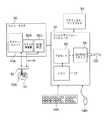
次に、図9を参照すると、本発明の一実施形態による方法が実行されるVLSIウェハ・テスト・システムが描写されている。ウェハ・テスタ50は、テスト対象のウェハ52上のダイ52Aへの電気テスト接続を有するプローブ・ヘッド53を介してダイ52Aに刺激を提供し、ダイ52Aからデータを検索するための境界スキャン・ユニット50Aを含む。ウェハ・テスタ50は、クロック発振器50Bによって生成され、プローブ・ヘッド53によってダイ52Aに供給される外部クロック信号の位相を評価する位相測定ユニット50Cを含む。 Referring now to FIG. 9, a VLSI wafer test system is depicted in which a method according to one embodiment of the present invention is performed.
メモリ57からのプログラム命令を実行するためにメモリ57に結合されたプロセッサ56を有するワークステーション・コンピュータ58であって、そのプログラム命令が本発明の一実施形態によるウェハ・テスタ50またはウェハ52内の回路あるいはその両方からデータを受け取るためのプログラム命令を含むワークステーション・コンピュータ58は、ウェハ・テスタ50に結合されている。一般に、本発明の方法は、遅延dl1〜dl3を設定し、測定のために特定のクロックおよびエッジを選択し、読み取りおよび書き込み操作によりストレージ・アレイ値にアクセスするように、スキャン・ユニット50Aを操作する。また、この方法は、測定対象の選択されたクロック信号の選択されたエッジの発生に対して外部クロック信号ext clkの位相も測定する。位相測定ユニット50Cの使用の代替策として、外部クロック信号ext clkのサイクルならびにテスタのスキャン・ユニット50Aを介してスキャン・チェーンから読み取られたカウンタ値をカウントするためにダイ回路内にカウンタを含めることもできる。プログラム命令は、ウェハ・テスタ50からカウントを入手するかまたはウェハ52からカウントを読み取り、次にそのカウントを処理して外部クロック信号ext clkの位相を入手する。プログラム命令は、CD−ROMドライブ55またはその他の適切な光学または磁気/不揮発性メモリ・ドライブを介して光ディスクCDなどの記憶媒体からロードすることができる。本発明の諸実施形態によって生成されたデータは、ダイ52内の記憶セル10のうちの特定のものまたはすべてに関する複数のテストから収集され、ストレージ・アレイ回路内のタイミング・マージンを完全に特徴付けるために変化する温度および電源電圧条件下で実行することができる。次に、すべての測定の結果を評価して、アレイ制御ロジックまたは記憶セル10の設計を変更するか、形成プロセスが許容できる標準から非常に逸脱しているかどうかを判断するか、あるいは電源電圧許容差およびアクセス・サイクル時間などの動作可能範囲を決定することができる。 A
本発明の諸実施形態による遅延/パルス幅テストからのデータは、ウェハ・テスタ50を介してワークステーション・コンピュータ58に転送され、メモリ57またはハード・ディスクなどのその他の記憶媒体あるいはその両方に保管される。ワークステーション・コンピュータ58は、測定されたエッジ位相または上記のメモリ・テストのパルス幅および遅延結果あるいはその両方などのプログラム出力を表示するためのグラフィカル・ディスプレイ59にも結合されている。また、グラフィカル・ディスプレイ59は、タイミング・マージン結果情報および測定値の分布を示すテキストまたは図形による結果も表示することができる。ワークステーション・コンピュータ58は、ユーザ入力を受け取るためのマウス54Bおよびキーボード54Aなどの入力装置にさらに結合されている。ワークステーション・コンピュータ58は、インターネットなどの公衆網に結合される場合もあれば、様々な「イントラネット」などの私設網に結合される場合もあり、本発明の諸実施形態による方法および回路によって生成されたデータを分析するためのプログラム命令を含むソフトウェアは、リモート・コンピュータ上に位置するかまたはワークステーション・コンピュータ58内にローカルに位置することができる。さらに、ワークステーション・コンピュータ58は、このようなネットワーク接続によってウェハ・テスタ50に結合することができる。 Data from delay / pulse width tests according to embodiments of the present invention is transferred to
図9のシステムはウェハ上の複数のダイの逐次テストに適した構成を描写しているが、描写されているシステムは例示的なものであり、本発明に制限するものではない。プローブ・ヘッド53は、マルチダイ・フルウェハ・プローブ・システムである場合もあれば、単一または複数ダイを基礎として複数のウェハを同時にテストするために複数のプローブ・ヘッドを含む場合もある。さらに、スキャン・チェーン・データ検索および刺激が例示されているが、本発明の技法は、プローブ・ウェハ52にとって使用可能な他のインターフェースにも適用するか、シリアルまたはパラレル・バスあるいはその他のインターフェースによりデータ抽出が実行される完全に機能しうるダイに実装された回路にも適用することができる。 Although the system of FIG. 9 depicts a configuration suitable for sequential testing of multiple dies on a wafer, the system depicted is exemplary and not limiting to the present invention. The
本発明はその好ましい実施形態に関連して詳細に示され記載されているが、当業者であれば、本発明の精神および範囲を逸脱せずに、形式および詳細について上記その他の変更を行うことができることを理解するであろう。 While the invention has been shown and described in detail in connection with preferred embodiments thereof, those skilled in the art will make other changes in form and detail without departing from the spirit and scope of the invention. You will understand that you can.
Claims (20)
Translated fromJapaneseローカル・クロック信号のアサート解除状態に応答して前記ビット線をプレチャージするためのプレチャージ回路と、
前記ローカル・クロック信号のアサート状態に応答して選択された行の前記ワード線選択入力を活動化するためのワード線制御ロジックと、
グローバル・クロック信号から前記ローカル・クロック信号を生成し、調整可能な遅延を有する少なくとも1つの遅延回路を含むプログラマブル・クロック制御ロジックであって、前記ローカル・クロック信号のタイミングおよびパルス幅が少なくとも1つの制御値に応じて調整され、それにより同一記憶セルの前記アレイの操作タイミング・マージンが調整可能であるプログラマブル・クロック制御ロジックと、
を含み、
前記ローカル・クロック信号のエッジを検出するためのエッジ検出器をさらに含み、それにより前記少なくとも1つの遅延回路の前記調整可能な遅延の大きさが前記エッジ検出器に提供される外部クロック信号の位相に関連して測定される、
記憶回路。A plurality of identical storage cells forming an array having rows and columns, wherein the storage cells in the column are connected by bit lines, and at least one bit line corresponding to each column has a read output signal for each column A plurality of identical storage cells connected to a corresponding one of a plurality of column read circuits for providing, each row having a corresponding word line select input connected to the storage cell in the corresponding row;
A precharge circuit for precharging the bit line in response to a deasserted state of the local clock signal;
Word line control logic for activating the word line select input of a selected row in response to the assertion state of the local clock signal;
Programmable clock control logic that generates the local clock signal from a global clock signal and includes at least one delay circuit having an adjustable delay, the timing and pulse width of the local clock signal being at least one Programmable clock control logic that is adjusted according to a control value, thereby adjusting an operation timing margin of the array of identical memory cells;
Only including,
A phase detector of the external clock signal, further comprising an edge detector for detecting an edge of the local clock signal, whereby the adjustable delay magnitude of the at least one delay circuit is provided to the edge detector; Measured in relation to the
Memory circuit.
少なくとも1つの制御値を前記ストレージ・アレイに提供するステップと、
前記少なくとも1つの制御値に応じて前記ストレージ・アレイ内の少なくとも1つの遅延回路を調整するステップであって、前記少なくとも1つの遅延回路が、前記アレイ内の記憶セル読み取りまたは書き込み操作を制御するローカル・クロック信号の少なくとも1つのエッジを遅延させパルス幅を調整するステップと、
前記少なくとも1つの制御値を変更することにより前記ローカル・クロック信号の前記少なくとも1つのエッジおよびパルス幅によって制御されるイベントの少なくとも1つのタイミング・マージンを決定するステップと、
を含み、
前記ローカル・クロック信号のエッジを検出するステップをさらに含み、それにより前記調整の大きさが前記ストレージ・アレイに提供される外部クロック信号の位相に関連して測定される、
方法。A method for measuring timing characteristics of a storage array, comprising:
Providing at least one control value to the storage array;
Adjusting at least one delay circuit in the storage array in response to the at least one control value, wherein the at least one delay circuit controls a storage cell read or write operation in the array. Delaying at least one edge of the clock signal and adjusting the pulse width;
Determining at least one timing margin of an event controlled by the at least one edge and a pulse width of the local clock signal by changing the at least one control value;
Only including,
Detecting an edge of the local clock signal, whereby the magnitude of the adjustment is measured in relation to the phase of an external clock signal provided to the storage array;
Method.
ローカル・クロック信号のアサート解除状態に応答して前記ビット線をプレチャージするためのプレチャージ回路と、
前記ローカル・クロック信号のアサート状態に応答して選択された行の前記ワード線選択入力を活動化するためのワード線制御ロジックと、
前記ビット線を入力として受け入れ、前記アレイから読み取られたデータ出力値を提供するための出力を有する読み取り回路であって、前記読み取り回路が遅延ローカル・クロック信号のアサート状態に応答して前記ビット線の状態を評価して前記データ出力値を決定し、前記遅延ローカル・クロック信号のアサート解除状態にさらに応答して前記データ出力値をラッチする読み取り回路と、
グローバル・クロック信号から前記ローカル・クロック信号および遅延クロック信号を生成し、第1の制御値に応じて前記ローカル・クロック信号のパルス幅を調整するための調整可能な遅延を有する第1の遅延回路と、第2の制御値に応じて前記ローカル・クロック信号に対して前記遅延ローカル・クロック信号のタイミングを調整するための第2の遅延回路と、第3の制御値に応じて前記遅延ローカル・クロック信号のパルス幅を調整するための第3の遅延回路とを含むプログラマブル・クロック制御ロジックであって、それにより前記第1の制御値を調整することにより読み取りまたは書き込みアクセス・タイミング・マージンが調整可能であり、前記第2の制御値を調整することにより前記読み取り回路のセットアップ・タイミング・マージンが調整可能であり、前記第3の制御値を調整することにより読み取り評価完了タイミング・マージンが調整可能であるプログラマブル・クロック制御ロジックと、
前記ローカル・クロック信号および前記遅延クロック信号のエッジを検出するためのエッジ検出器であって、それにより前記第1の遅延回路、前記第2の遅延回路、および前記第3の遅延回路の前記調整可能な遅延の大きさが前記エッジ検出器に提供される外部クロック信号の位相に関連して測定されるエッジ検出器と、
を含む、記憶回路。A plurality of identical storage cells forming an array having rows and columns, wherein the storage cells in the column are connected by bit lines, and at least one bit line corresponding to each column has a read output signal for each column A plurality of identical storage cells connected to a corresponding one of a plurality of column read circuits for providing, each row having a corresponding word line select input connected to the storage cell in the corresponding row;
A precharge circuit for precharging the bit line in response to a deasserted state of the local clock signal;
Word line control logic for activating the word line select input of a selected row in response to the assertion state of the local clock signal;
A read circuit having an output for accepting the bit line as an input and providing a data output value read from the array, wherein the read circuit is responsive to an asserted state of a delayed local clock signal A read circuit that evaluates the state of the data to determine the data output value, and further latches the data output value in response to the de-asserted state of the delayed local clock signal;
A first delay circuit having an adjustable delay for generating the local clock signal and the delayed clock signal from a global clock signal and adjusting a pulse width of the local clock signal according to a first control value A second delay circuit for adjusting a timing of the delayed local clock signal with respect to the local clock signal according to a second control value, and the delayed local clock according to a third control value. A programmable clock control logic including a third delay circuit for adjusting a pulse width of the clock signal, thereby adjusting a read or write access timing margin by adjusting the first control value Is possible, and by adjusting the second control value, setup timing of the reading circuit Margin is adjustable, and the programmable clock control logic is adjustable read evaluation completion timing margin by adjusting the third control value,
An edge detector for detecting edges of the local clock signal and the delayed clock signal, whereby the adjustment of the first delay circuit, the second delay circuit, and the third delay circuit; An edge detector in which the amount of possible delay is measured in relation to the phase of an external clock signal provided to the edge detector;
Including a memory circuit.
第1の制御値、第2の制御値、および第3の制御値を前記ストレージ・アレイに提供するステップと、
前記第1の制御値に応じて前記ストレージ・アレイ内の第1の遅延回路を調整する第1の調整ステップであって、前記第1の遅延回路が、前記アレイ内の記憶セル読み取りまたは書き込み操作を制御するローカル・クロック信号のパルス幅を制御する、第1の調整ステップと、
前記第2の制御値に応じて前記ストレージ・アレイ内の第2の遅延回路を調整する第2の調整ステップであって、前記第2の遅延回路が、前記ローカル・クロック信号に対して前記ストレージ・アレイ内の読み取り評価を制御する遅延ローカル・クロック信号のタイミングを制御する、第2の調整ステップと、
前記第3の制御値に応じて前記ストレージ・アレイ内の第3の遅延回路を調整する第3の調整ステップであって、前記第3の遅延回路が、前記遅延ローカル・クロック信号のパルス幅を制御する、第3の調整ステップと、
前記第1の制御値を変更することにより読み取りまたは書き込みアクセス・タイミング・マージンを決定するステップと、
前記第2の制御値を変更することによりセットアップ・タイミング・マージンを決定するステップと、
前記第3の制御値を変更することにより読み取り評価完了タイミング・マージンを決定するステップと、
前記ローカル・クロック信号および前記遅延ローカル・クロック信号のエッジを検出するステップであって、それにより前記第1、第2、および第3の調整の大きさが前記ストレージ・アレイに提供される外部クロック信号の位相に関連して測定されるステップと、
を含む、方法。A method for measuring timing characteristics of a storage array, comprising:
Providing a first control value, a second control value, and a third control value to the storage array;
A first adjustment step of adjusting a first delay circuit in the storage array in accordance with the first control value, wherein the first delay circuit performs a read or write operation on a storage cell in the array; A first adjusting step for controlling a pulse width of a local clock signal for controlling
A second adjustment step of adjusting a second delay circuit in the storage array according to the second control value, wherein the second delay circuit is configured to store the storage with respect to the local clock signal; A second adjustment step that controls the timing of the delayed local clock signal that controls the read evaluation within the array;
A third adjustment step of adjusting a third delay circuit in the storage array according to the third control value, wherein the third delay circuit sets a pulse width of the delayed local clock signal; A third adjusting step to control;
Determining a read or write access timing margin by changing the first control value;
Determining a setup timing margin by changing the second control value;
Determining a read evaluation completion timing margin by changing the third control value;
Detecting an edge of the local clock signal and the delayed local clock signal, whereby the magnitudes of the first, second and third adjustments are provided to the storage array; Steps measured in relation to the phase of the signal;
Including a method.
Applications Claiming Priority (3)
| Application Number | Priority Date | Filing Date | Title |
|---|---|---|---|
| US11/935,566 | 2007-11-06 | ||
| US11/935,566US7668037B2 (en) | 2007-11-06 | 2007-11-06 | Storage array including a local clock buffer with programmable timing |
| PCT/KR2008/006336WO2009061093A2 (en) | 2007-11-06 | 2008-10-28 | Storage array including a local clock buffer with programmable timing |
Publications (2)
| Publication Number | Publication Date |
|---|---|
| JP2011503766A JP2011503766A (en) | 2011-01-27 |
| JP5437258B2true JP5437258B2 (en) | 2014-03-12 |
Family
ID=40587959
Family Applications (1)
| Application Number | Title | Priority Date | Filing Date |
|---|---|---|---|
| JP2010532997AExpired - Fee RelatedJP5437258B2 (en) | 2007-11-06 | 2008-10-28 | Method for measuring timing characteristics of storage circuits and storage arrays (storage arrays including local clock buffers with programmable timing) |
Country Status (4)
| Country | Link |
|---|---|
| US (1) | US7668037B2 (en) |
| JP (1) | JP5437258B2 (en) |
| KR (1) | KR101174568B1 (en) |
| WO (1) | WO2009061093A2 (en) |
Families Citing this family (22)
| Publication number | Priority date | Publication date | Assignee | Title |
|---|---|---|---|---|
| US7760565B2 (en)* | 2007-07-24 | 2010-07-20 | International Business Machines Corporation | Wordline-to-bitline output timing ring oscillator circuit for evaluating storage array performance |
| US7659749B2 (en)* | 2007-10-22 | 2010-02-09 | International Business Machines Corporation | Pulsed dynamic logic environment metric measurement circuit |
| US8219857B2 (en)* | 2008-06-26 | 2012-07-10 | International Business Machines Corporation | Temperature-profiled device fingerprint generation and authentication from power-up states of static cells |
| US7880505B2 (en)* | 2009-02-20 | 2011-02-01 | Sunil Papanchand Khatri | Low power reconfigurable circuits with delay compensation |
| KR101716714B1 (en) | 2010-04-01 | 2017-03-16 | 삼성전자주식회사 | Semiconductor memory device synchronized to clock signal |
| US8345497B2 (en) | 2010-06-23 | 2013-01-01 | International Business Machines Corporation | Internal bypassing of memory array devices |
| US8345490B2 (en) | 2010-06-23 | 2013-01-01 | International Business Machines Corporation | Split voltage level restore and evaluate clock signals for memory address decoding |
| US8351278B2 (en) | 2010-06-23 | 2013-01-08 | International Business Machines Corporation | Jam latch for latching memory array output data |
| US8599642B2 (en) | 2010-06-23 | 2013-12-03 | International Business Machines Corporation | Port enable signal generation for gating a memory array device output |
| US8754691B2 (en) | 2012-09-27 | 2014-06-17 | International Business Machines Corporation | Memory array pulse width control |
| US8643168B1 (en) | 2012-10-16 | 2014-02-04 | Lattice Semiconductor Corporation | Integrated circuit package with input capacitance compensation |
| US10324841B2 (en)* | 2013-07-27 | 2019-06-18 | Netlist, Inc. | Memory module with local synchronization |
| US9019752B1 (en) | 2013-11-26 | 2015-04-28 | Qualcomm Incorporated | Static random access memory (SRAM) global bitline circuits for reducing power glitches during memory read accesses, and related methods and systems |
| US9070433B1 (en) | 2014-03-11 | 2015-06-30 | International Business Machines Corporation | SRAM supply voltage global bitline precharge pulse |
| US10230360B2 (en)* | 2017-06-16 | 2019-03-12 | International Business Machines Corporation | Increasing resolution of on-chip timing uncertainty measurements |
| DE102018128927B4 (en)* | 2018-08-31 | 2024-06-27 | Taiwan Semiconductor Manufacturing Co., Ltd. | Wordline activation for variable delay |
| JP2020042873A (en)* | 2018-09-11 | 2020-03-19 | 株式会社東芝 | Semiconductor storage device |
| US10901454B2 (en) | 2019-02-06 | 2021-01-26 | Qualcomm Incorporated | Clock buffering to reduce memory hold time |
| CN112767977B (en) | 2020-12-31 | 2023-09-26 | 深圳市紫光同创电子有限公司 | Read and write window calibration circuit and method, memory, FPGA chip |
| US11456729B1 (en) | 2021-03-26 | 2022-09-27 | Analog Devices, Inc. | Deskew cell for delay and pulse width adjustment |
| US11947891B2 (en) | 2021-08-20 | 2024-04-02 | International Business Machines Corporation | Balancing cycle stealing with early mode violations |
| US12204287B2 (en)* | 2022-08-02 | 2025-01-21 | Apple Inc. | Multi-chain measurement circuit |
Family Cites Families (22)
| Publication number | Priority date | Publication date | Assignee | Title |
|---|---|---|---|---|
| US4603292A (en)* | 1984-04-03 | 1986-07-29 | Honeywell Information Systems Inc. | Frequency and time measurement circuit |
| US4769791A (en)* | 1986-08-06 | 1988-09-06 | Advanced Micro Devices, Inc. | On-chip pulse-width control circuit for SRAM memories |
| JP2509275B2 (en)* | 1988-02-02 | 1996-06-19 | 富士通株式会社 | Semiconductor memory device |
| US5122978A (en)* | 1989-09-07 | 1992-06-16 | Amdahl Corporation | Pulse width measurement technique |
| JPH03230395A (en)* | 1990-02-02 | 1991-10-14 | Hitachi Ltd | Static type ram |
| JP2606082B2 (en)* | 1993-07-02 | 1997-04-30 | 日本電気株式会社 | Semiconductor integrated circuit |
| JP3523718B2 (en)* | 1995-02-06 | 2004-04-26 | 株式会社ルネサステクノロジ | Semiconductor device |
| JP2001052497A (en)* | 1999-08-05 | 2001-02-23 | Mitsubishi Electric Corp | Semiconductor memory failure information acquisition method, semiconductor memory repair analysis device, and semiconductor memory device |
| JP2001052498A (en)* | 1999-08-05 | 2001-02-23 | Toshiba Corp | Semiconductor storage device |
| JP4301680B2 (en)* | 2000-02-29 | 2009-07-22 | 株式会社ルネサステクノロジ | Semiconductor integrated circuit device |
| WO2002005281A2 (en)* | 2000-07-07 | 2002-01-17 | Mosaid Technologies Incorporated | A high speed dram architecture with uniform access latency |
| JP2002042466A (en)* | 2000-07-21 | 2002-02-08 | Mitsubishi Electric Corp | Semiconductor device and semiconductor storage device |
| JP2002196053A (en) | 2000-12-25 | 2002-07-10 | Ando Electric Co Ltd | Ic measurement device |
| US6728912B2 (en)* | 2001-04-12 | 2004-04-27 | International Business Machines Corporation | SOI cell stability test method |
| US6549452B1 (en)* | 2001-12-20 | 2003-04-15 | Integrated Device Technology, Inc. | Variable width wordline pulses in a memory device |
| JP2003242799A (en)* | 2002-02-12 | 2003-08-29 | Hitachi Ltd | Semiconductor integrated circuit |
| JP2004158144A (en)* | 2002-11-07 | 2004-06-03 | Renesas Technology Corp | Semiconductor integrated circuit |
| JP2004178729A (en)* | 2002-11-28 | 2004-06-24 | Hitachi Ltd | Semiconductor storage device |
| DE602004007349T2 (en)* | 2004-01-15 | 2008-03-13 | Infineon Technologies Ag | Device for determining the access time and / or the minimum cycle time of a memory |
| US7236555B2 (en)* | 2004-01-23 | 2007-06-26 | Sunrise Telecom Incorporated | Method and apparatus for measuring jitter |
| US7272061B2 (en) | 2005-01-24 | 2007-09-18 | Intel Corporation | Dynamic pre-charge level control in semiconductor devices |
| WO2007099579A1 (en)* | 2006-02-28 | 2007-09-07 | Fujitsu Limited | Ram macro and timing generating circuit for same |
- 2007
- 2007-11-06USUS11/935,566patent/US7668037B2/enactiveActive
- 2008
- 2008-10-28KRKR1020107009256Apatent/KR101174568B1/ennot_activeExpired - Fee Related
- 2008-10-28JPJP2010532997Apatent/JP5437258B2/ennot_activeExpired - Fee Related
- 2008-10-28WOPCT/KR2008/006336patent/WO2009061093A2/enactiveApplication Filing
Also Published As
| Publication number | Publication date |
|---|---|
| US20090116312A1 (en) | 2009-05-07 |
| KR20100075564A (en) | 2010-07-02 |
| US7668037B2 (en) | 2010-02-23 |
| WO2009061093A2 (en) | 2009-05-14 |
| WO2009061093A3 (en) | 2009-07-02 |
| JP2011503766A (en) | 2011-01-27 |
| KR101174568B1 (en) | 2012-08-16 |
Similar Documents
| Publication | Publication Date | Title |
|---|---|---|
| JP5437258B2 (en) | Method for measuring timing characteristics of storage circuits and storage arrays (storage arrays including local clock buffers with programmable timing) | |
| US7564739B2 (en) | Storage cell design evaluation circuit including a wordline timing and cell access detection circuit | |
| US7620510B2 (en) | Pulsed ring oscillator circuit for storage cell read timing evaluation | |
| US7760565B2 (en) | Wordline-to-bitline output timing ring oscillator circuit for evaluating storage array performance | |
| US7376001B2 (en) | Row circuit ring oscillator method for evaluating memory cell performance | |
| US7515491B2 (en) | Method for evaluating leakage effects on static memory cell access time | |
| JP3544203B2 (en) | Test circuit, semiconductor integrated circuit device incorporating the test circuit, and test method thereof | |
| JP5134558B2 (en) | Data processing apparatus and method for testing the stability of memory cells in a memory device | |
| TWI620197B (en) | A memory device and method of performing access operations within such a memory device | |
| US6885610B2 (en) | Programmable delay for self-timed-margin | |
| US7355902B2 (en) | Methods and apparatus for inline characterization of high speed operating margins of a storage element | |
| US7304895B2 (en) | Bitline variable methods and circuits for evaluating static memory cell dynamic stability | |
| Arslan et al. | Variation-tolerant SRAM sense-amplifier timing using configurable replica bitlines | |
| US20100142300A1 (en) | Semiconductor Memory Device And Methods Of Performing A Stress Test On The Semiconductor Memory Device | |
| Kinseher et al. | Improving testability and reliability of advanced SRAM architectures | |
| TWI631571B (en) | Negative bias thermal instability stress testing for static random access memory (sram) | |
| GB2464126A (en) | Storage array including a local clock buffer with adjustable timing | |
| JP3705759B2 (en) | Synchronous semiconductor memory device | |
| Joshi et al. | A high performance 2.4 Mb L1 and L2 cache compatible 45nm SRAM with yield improvement capabilities | |
| Ataei et al. | A unified memory compiler for synchronous and asynchronous circuits | |
| US20250251449A1 (en) | Innovative sram in-silicon monitor circuit and system implementation | |
| Vaghasia | Design & Characterization Of HD1P and HS1P Memory Compiler | |
| Joshi et al. | Statistical-aware Designs for the nm Era |
Legal Events
| Date | Code | Title | Description |
|---|---|---|---|
| A621 | Written request for application examination | Free format text:JAPANESE INTERMEDIATE CODE: A621 Effective date:20110922 | |
| A131 | Notification of reasons for refusal | Free format text:JAPANESE INTERMEDIATE CODE: A131 Effective date:20121204 | |
| A521 | Request for written amendment filed | Free format text:JAPANESE INTERMEDIATE CODE: A523 Effective date:20130301 | |
| A131 | Notification of reasons for refusal | Free format text:JAPANESE INTERMEDIATE CODE: A131 Effective date:20130723 | |
| A521 | Request for written amendment filed | Free format text:JAPANESE INTERMEDIATE CODE: A523 Effective date:20131011 | |
| TRDD | Decision of grant or rejection written | ||
| A01 | Written decision to grant a patent or to grant a registration (utility model) | Free format text:JAPANESE INTERMEDIATE CODE: A01 Effective date:20131119 | |
| A61 | First payment of annual fees (during grant procedure) | Free format text:JAPANESE INTERMEDIATE CODE: A61 Effective date:20131211 | |
| R150 | Certificate of patent or registration of utility model | Ref document number:5437258 Country of ref document:JP Free format text:JAPANESE INTERMEDIATE CODE: R150 Free format text:JAPANESE INTERMEDIATE CODE: R150 | |
| R250 | Receipt of annual fees | Free format text:JAPANESE INTERMEDIATE CODE: R250 | |
| R250 | Receipt of annual fees | Free format text:JAPANESE INTERMEDIATE CODE: R250 | |
| LAPS | Cancellation because of no payment of annual fees |