Movatterモバイル変換


[0]ホーム

URL:


JP5435286B2 - Drive device - Google Patents

Drive device
Download PDF

Info

Publication number
JP5435286B2
JP5435286B2JP2010117686AJP2010117686AJP5435286B2JP 5435286 B2JP5435286 B2JP 5435286B2JP 2010117686 AJP2010117686 AJP 2010117686AJP 2010117686 AJP2010117686 AJP 2010117686AJP 5435286 B2JP5435286 B2JP 5435286B2
Authority
JP
Japan
Prior art keywords
heat sink
motor
side wall
semiconductor modules
electronic circuit
Prior art date
Legal status (The legal status is an assumption and is not a legal conclusion. Google has not performed a legal analysis and makes no representation as to the accuracy of the status listed.)
Active
Application number
JP2010117686A
Other languages
Japanese (ja)
Other versions
JP2011177001A (en
Inventor
雅志 山▲崎▼
秀樹 株根
敦司 古本
Current Assignee (The listed assignees may be inaccurate. Google has not performed a legal analysis and makes no representation or warranty as to the accuracy of the list.)
Denso Corp
Original Assignee
Denso Corp
Priority date (The priority date is an assumption and is not a legal conclusion. Google has not performed a legal analysis and makes no representation as to the accuracy of the date listed.)
Filing date
Publication date
Priority to JP2010117686ApriorityCriticalpatent/JP5435286B2/en
Application filed by Denso CorpfiledCriticalDenso Corp
Priority to CN201080028286.4Aprioritypatent/CN102804559B/en
Priority to PCT/JP2010/004156prioritypatent/WO2010150527A1/en
Priority to CN201210013678.4Aprioritypatent/CN102570694B/en
Priority to DE112010004321.3Tprioritypatent/DE112010004321B4/en
Priority to US13/380,321prioritypatent/US8957557B2/en
Priority to DE112010002719.6Tprioritypatent/DE112010002719B4/en
Publication of JP2011177001ApublicationCriticalpatent/JP2011177001A/en
Priority to US13/336,492prioritypatent/US8710705B2/en
Application grantedgrantedCritical
Publication of JP5435286B2publicationCriticalpatent/JP5435286B2/en
Activelegal-statusCriticalCurrent
Anticipated expirationlegal-statusCritical

Links

Images

Classifications

Landscapes

Description

Translated fromJapanese

本発明は、モータと電子回路とを一体にした駆動装置に関する。  The present invention relates to a drive device in which a motor and an electronic circuit are integrated.

近年、車両のステアリングの取り回しを補助する機構として、油圧式でトルクを発生させる油圧アシスト装置に代わり、電動式でトルクを発生させる電動アシスト装置が注目されている。電動アシスト装置では、油圧式と異なり、運転者のステアリング操作があったときにだけアシストが行われる。そのため、低燃費の実現などメリットが多い。  2. Description of the Related Art In recent years, as a mechanism for assisting steering of a vehicle, an electric assist device that generates electric torque has attracted attention, instead of a hydraulic assist device that generates torque. In the electric assist device, unlike the hydraulic type, the assist is performed only when the driver performs a steering operation. Therefore, there are many advantages such as low fuel consumption.

電動アシスト装置の動力発生源としてのモータには、例えば三相交流を印加することで回転駆動されるブラシレスモータがある。このようなブラシレスモータを用いる場合、複数相(例えば三相)の巻線へ位相の異なる巻線電流を供給するため、所定電圧(例えば12V)の直流出力から位相がずれた交流出力を作り出す必要がある。したがって、巻線電流を切り換えるための電子回路が必要となってくる。ここで特に、電子回路には、スイッチング機能を実現する半導体モジュール及び、全体の制御を司るマイコン等が含まれる。  As a motor as a power generation source of the electric assist device, for example, there is a brushless motor that is rotationally driven by applying a three-phase alternating current. When using such a brushless motor, in order to supply winding currents having different phases to a plurality of (for example, three-phase) windings, it is necessary to create an AC output that is out of phase with a DC output of a predetermined voltage (for example, 12V). There is. Therefore, an electronic circuit for switching the winding current is required. Here, in particular, the electronic circuit includes a semiconductor module that realizes a switching function, a microcomputer that performs overall control, and the like.

従来、このような電子回路をモータの近傍に配置したものが開示されている。例えば、半導体モジュールをモータの軸方向に配置したもの(例えば、特許文献1、2参照)、あるいは、モータを構成するステータの周囲に配置したものが挙げられる(例えば、特許文献3参照)。  Conventionally, an electronic circuit in which such an electronic circuit is arranged in the vicinity of a motor has been disclosed. For example, a semiconductor module may be arranged in the axial direction of the motor (for example, seePatent Documents 1 and 2), or a semiconductor module may be arranged around a stator constituting the motor (for example, see Patent Document 3).

特開平10−234158号公報Japanese Patent Laid-Open No. 10-234158特開平10−322973号公報Japanese Patent Laid-Open No. 10-322973特開2004−159454号公報JP 2004-159454 A特開2002−120739号公報Japanese Patent Laid-Open No. 2002-120739

ところで、電動アシスト装置では、十分なトルクを得るため、比較的大きなモータが使用される。このため、半導体モジュールの体格は大きなものとなる。また、スイッチングにより発生するサージ電圧によって半導体チップが破壊されることを防止する等の目的から、体格の大きなコンデンサ(例えばアルミ電解コンデンサ)を電子回路に設けるのが一般的である。  By the way, in the electric assist device, a relatively large motor is used in order to obtain a sufficient torque. For this reason, the size of the semiconductor module becomes large. Also, for the purpose of preventing the semiconductor chip from being destroyed by a surge voltage generated by switching, it is common to provide a large-sized capacitor (for example, an aluminum electrolytic capacitor) in the electronic circuit.

ところが、電動アシスト装置以外にも車両に種々の装置が取り付けられる昨今においては、各種装置の取り付けに必要なスペースの確保が重要な課題となっている。結果として、電動アシスト装置のモータに対しても小型化の要請が益々強くなっている。  However, in recent years when various devices other than the electric assist device are mounted on the vehicle, it is important to secure a space necessary for mounting the various devices. As a result, there is an increasing demand for miniaturization of the motor of the electric assist device.

この点、例えば特許文献1、2に記載されたモータでは、半導体モジュールとコンデンサとがモータの軸方向に並べて配置されている。結果として、モータの軸方向の体格が大きくなってしまうという問題がある。  In this regard, for example, in the motors described inPatent Documents 1 and 2, the semiconductor module and the capacitor are arranged side by side in the axial direction of the motor. As a result, there is a problem that the physique in the axial direction of the motor becomes large.

また例えば特許文献3に記載されたモータでは、半導体モジュールがステータの周囲に配置されており、モータの軸方向の体格は小さくなるものの、モータの径方向の体格が大きくなってしまうという問題がある。しかも、ここに用いられている平滑用コンデンサは平型のものであるが、例えば円筒状のコンデンサを使用しなければならない状況下では、径方向の体格が一層大きくなるものと思われる。  Further, for example, in the motor described inPatent Document 3, the semiconductor module is arranged around the stator, and although the physique in the axial direction of the motor becomes small, the physique in the radial direction of the motor becomes large. . Moreover, although the smoothing capacitor used here is a flat type, for example, in a situation where a cylindrical capacitor must be used, it seems that the physique in the radial direction is further increased.

本発明は、上述した問題を解決するためになされたものであり、その目的は、駆動制御のための電子回路とモータとを一体化した駆動装置において、その体格を可及的に小さくすることにある。  The present invention has been made to solve the above-described problems, and an object of the present invention is to reduce the physique as much as possible in a drive device in which an electronic circuit for drive control and a motor are integrated. It is in.

上述した課題を解決するためになされた請求項1に記載の駆動装置は、モータと、電子回路とを備えている。モータの外郭は筒状のモータケースにて形成されている。ここでいう「筒状」は円筒状には限定されない。このモータケースの径方向内側には、ステータが配置される。ステータは、複数相を構成するよう巻線が巻回されてなる。さらにステータの径方向内側に配置されるのがロータであり、このロータと共にシャフトは回転する。さらにまた、モータケースの端部からは、ヒートシンクが、シャフトの中心線方向と同方向へ延設されている。なお、以下では、必要に応じて適宜「シャフトの中心線」を単に「軸線」と記載し、「シャフトの中心線方向」を単に「軸方向」と記載する。  The drive device according toclaim 1, which has been made to solve the above-described problem, includes a motor and an electronic circuit. The outer shell of the motor is formed by a cylindrical motor case. The “tubular shape” here is not limited to a cylindrical shape. A stator is disposed inside the motor case in the radial direction. The stator is formed by winding a winding so as to constitute a plurality of phases. Further, a rotor is disposed on the radially inner side of the stator, and the shaft rotates together with the rotor. Furthermore, a heat sink is extended from the end of the motor case in the same direction as the center line direction of the shaft. In the following description, the “shaft center line” is simply referred to as “axial line” and the “shaft center line direction” is simply referred to as “axial direction” as appropriate.

電子回路は、モータケースに対しシャフトの中心線方向におけるヒートシンク側に配置される。つまり、モータの軸方向に配置されるのである。ただし、例えば円筒状のモータケースを考えた場合、軸方向へモータケースを仮想的に延長したモータシルエット内に完全に電子回路が収まることまで限定する趣旨ではない。  The electronic circuit is arranged on the heat sink side in the direction of the center line of the shaft with respect to the motor case. That is, it is arranged in the axial direction of the motor. However, for example, when a cylindrical motor case is considered, it is not intended to limit the electronic circuit to be completely contained in a motor silhouette obtained by virtually extending the motor case in the axial direction.

ここで、電子回路は、複数相の巻線に流れる巻線電流を切り換えるための半導体チップを具備する半導体モジュールを有している。例えば、半導体チップには半導体スイッチ素子が構成されており、この半導体スイッチ素子のオン/オフによって、巻線電流が切り換えられるという具合である。  Here, the electronic circuit has a semiconductor module including a semiconductor chip for switching a winding current flowing in a plurality of phase windings. For example, a semiconductor switch element is configured in the semiconductor chip, and the winding current is switched by turning on / off the semiconductor switch element.

また、電子回路は、半導体モジュールの給電側から電源までのラインと半導体モジュールの接地側からグランドまでのラインとの間に並列に接続されるコンデンサを有している。言い換えれば、コンデンサの一方の端子は、電源から半導体モジュールへ到るラインの途中に接続され、コンデンサの他方の端子は、半導体モジュールからグランドへ到るラインの途中に接続される。コンデンサは、半導体モジュールの電源ラインとグランドとの間に接続されることで、例えばサージ電圧などのノイズ成分を抑制したり、また例えば半導体スイッチ素子等への電力供給を補助したりする。
さらに、電子回路は、ヒートシンクの径方向内側に配置され、半導体モジュールの電源ラインに介在するチョークコイルを有している。
The electronic circuit also includes a capacitor connected in parallel between a line from the power supply side of the semiconductor module to the power source and a line from the ground side of the semiconductor module to the ground. In other words, one terminal of the capacitor is connected in the middle of the line from the power source to the semiconductor module, and the other terminal of the capacitor is connected in the middle of the line from the semiconductor module to the ground. The capacitor is connected between the power supply line of the semiconductor module and the ground, thereby suppressing a noise component such as a surge voltage or assisting power supply to the semiconductor switch element or the like, for example.
Further, the electronic circuit has a choke coil that is disposed on the radially inner side of the heat sink and interposed in the power supply line of the semiconductor module.

従来は、2枚のプリント基板がモータの軸方向に間隔を空けて設けられており、半導体モジュールとコンデンサとは、プリント基板を隔てて軸方向に並べて配置されている(例えば、特許文献1、2参照)。したがって、モータの軸方向の体格が大きくなってしまっている。  Conventionally, two printed circuit boards are provided with an interval in the axial direction of the motor, and the semiconductor module and the capacitor are arranged side by side in the axial direction with the printed circuit board being separated (for example,Patent Document 1, 2). Therefore, the physique in the axial direction of the motor has increased.

そこで、本発明では、半導体モジュールを縦配置とした。半導体モジュールが縦配置されるとは、半導体チップ面の垂線が軸線に対し非平行となっていることをいう。詳しくは、ヒートシンクの側壁に接触するようにして半導体モジュールを縦配置する。なお、「ヒートシンクの側壁に直接的に又は間接的に接触する」とあるのは、放熱を促進するための構成であり、直接的に接触することだけでなく、絶縁シートを挟み込んだ状態で接触することも含める趣旨である。これにより、軸方向において、半導体モジュール、ヒートシンク、及び、コンデンサのそれぞれの配置範囲の少なくとも一部が重なるよう構成した。例えば、径方向に並べて配置するという具合である。  Therefore, in the present invention, the semiconductor module is arranged vertically. The term “semiconductor module is vertically arranged” means that the perpendicular to the semiconductor chip surface is not parallel to the axis. Specifically, the semiconductor module is vertically arranged so as to be in contact with the side wall of the heat sink. Note that “directly or indirectly contact the heat sink side wall” is a configuration for promoting heat dissipation, not only directly contacting, but also in a state of sandwiching an insulating sheet. The purpose is to include. Accordingly, at least a part of the arrangement range of each of the semiconductor module, the heat sink, and the capacitor is overlapped in the axial direction. For example, they are arranged side by side in the radial direction.

このように本発明では、その前提として電子回路をモータの軸方向に配置しているため、ステータの周りに半導体モジュールを配置する構成(例えば、特許文献3参照)と比べ、径方向の体格を小さくすることができる。しかも、半導体モジュールを縦配置とし確保されるスペースを利用して軸方向におけるヒートシンク、半導体モジュール及びコンデンサのそれぞれの配置範囲が重なるように配置したため、従来の構成と異なり(例えば、特許文献1、2参照)軸方向の体格をも小さくすることができる。その結果、駆動装置の体格を可及的に小さくすることができる。
また、ヒートシンクを構成する側壁の内側にチョークコイルを収容するため、体格の比較的大きなチョークコイルを使用する場合でも、駆動装置の体格を可及的に小さくすることができる。さらに、本発明では、中心線方向において、半導体モジュール、ヒートシンク、及び、チョークコイルが重なっていることを特徴とする。
As described above, in the present invention, the electronic circuit is arranged in the axial direction of the motor as a premise thereof, so that the physique in the radial direction is made larger than the configuration in which the semiconductor module is arranged around the stator (for example, see Patent Document 3). Can be small. In addition, since the semiconductor modules are arranged so that the arrangement ranges of the heat sink, the semiconductor module, and the capacitor in the axial direction overlap with each other by using a space that is secured in a vertical arrangement, the arrangement differs from the conventional configuration (for example,Patent Documents 1 and 2). See also: Axial physique can be reduced. As a result, the size of the drive device can be made as small as possible.
Further, since the choke coil is accommodated inside the side wall constituting the heat sink, the physique of the driving device can be made as small as possible even when a relatively large sized choke coil is used. Furthermore, the present invention is characterized in that the semiconductor module, the heat sink, and the choke coil overlap in the center line direction.

このように「半導体モジュールの縦配置によるスペースの確保」、及び「当該スペースの有効利用によるコンデンサ及びヒートシンクの配置」という思想は、機電一体型を超える「機電融合型」と言い得る。  As described above, the concepts of “securing space by vertically arranging semiconductor modules” and “arranging capacitors and heat sinks by effectively using the space” can be referred to as “mechanical fusion type” exceeding the mechanical / electrical type.

半導体モジュールの配置について言えば、請求項2に示すように、それぞれが異なる平面を規定する複数の側壁面をヒートシンクが有していることを前提として、半導体モジュールは、複数の側壁面のうちの2以上の側壁面に分散配置し、チョークコイルをヒートシンクの中心に形成された空間に配置してもよい。つまり、半導体チップ面が同一平面上に位置しないよう半導体モジュールを配置するのである。例えば、軸方向に見て半導体モジュールを円周上に配置するという具合である。このとき、半導体チップ面が円の法線に垂直となるようにすれば、半導体チップ面が同一平面上に位置することはない。With regard to the arrangement of the semiconductor modules, as shown inclaim 2, on the assumption that the heat sink has a plurality of side wall surfaces each defining a different plane, the semiconductor module is formed of the plurality of side wall surfaces. Thechoke coil may bearranged in a space formed in the center of the heat sink by being distributed on two or more side wall surfaces. That is, the semiconductor module is arranged so that the semiconductor chip surface is not located on the same plane. For example, the semiconductor modules are arranged on the circumference when viewed in the axial direction. At this time, if the semiconductor chip surface is perpendicular to the normal line of the circle, the semiconductor chip surface will not be located on the same plane.

半導体モジュールに対するコンデンサ及びヒートシンクの配置は、請求項3に示すように、コンデンサを、半導体モジュールに対しヒートシンクと同じ側に配置し、ヒートシンクに形成された収容部にコンデンサを収容する構成が考えられる。このようにヒートシンクに収容部を形成するとヒートシンクの熱容量が若干低下するものの、半導体モジュールの一側にヒートシンク及びコンデンサが配置されるため、他側にスペースが確保できるという点で有利である。Arrangement of capacitors and the heat sink for the semiconductor module, as shown inclaim 3, a capacitor,arranged on the same side as the heat sink to the semiconductormodule, configuration isthought to accommodate the capacitor in the accommodation section formed in the heat sink . When the housing portion is formed on the heat sink in this manner, although the heat capacity of the heat sink is slightly reduced, the heat sink and the capacitor are arranged on one side of the semiconductor module, which is advantageous in that a space can be secured on the other side.

一方、請求項に示すように、コンデンサを、半導体モジュールに対しヒートシンクの反対側に配置することが考えられる。このようにすれば、全体としての配置スペースは例えば径方向に大きくなるものの、コンデンサ用の収容部をヒートシンクに形成する必要がなくなる。On the other hand, as shown inclaim4 , it is conceivable to arrange the capacitor on the opposite side of the heat sink with respect to the semiconductor module. In this way, the overall arrangement space becomes larger in the radial direction, for example, but there is no need to form a capacitor housing in the heat sink.

また、請求項に示すように、相互に離間する複数の側壁をヒートシンクが有する構成とし、半導体モジュールが、複数の駆動系統に対応するよう設けられ、一つの側壁に対し一つの駆動系統が対応するように側壁に配置されていることとしてもよい。このようにすれば、半導体モジュールで発生する熱をバランス良く分散させることができる。また、各駆動系統に属する半導体モジュールを異なる側壁に配置したため、同一箇所にまとめて配置する構成と異なり、各駆動系統が同時期に故障することを防止できる。According to afifth aspect of the present invention, the heat sink has a plurality of side walls spaced apart from each other, and the semiconductor module is provided so as to correspond to a plurality of drive systems, and one drive system corresponds to one side wall. It is good also as arrange | positioning at a side wall so that. In this way, the heat generated in the semiconductor module can be dispersed with a good balance. Moreover, since the semiconductor modules belonging to each drive system are arranged on different side walls, it is possible to prevent each drive system from failing at the same time, unlike a configuration in which the semiconductor modules are arranged together in the same place.

ところで、上記側壁は、請求項に示すように、径方向に所定の厚みを有する厚肉板状を呈し、その端部に、軸方向に貫通する固定用穴が形成された接続部を有することとしてもよい。板状とすることにより、半導体モジュールを配置するスペースが確保されるためである。By the way, as shown inclaim6 , the side wall has a thick plate shape having a predetermined thickness in the radial direction, and hasa connection portion formed with a fixing hole penetrating in the axial direction at an end thereof. it may beto Rukoto. This is because a space for arranging the semiconductor module is secured by using the plate shape.

また、このようにすれば、モータケースなどに対して側壁、すなわちヒートシンクを簡単に固定することができる。なお、各側壁が別体となっていてヒートシンクを構成してもよいし、各側壁が互いに連結されて単一のヒートシンクを構成してもよい。Further, if asthis, it is possible to respect a motor case side wall, i.e. easy to secure the heat sink. Each side wall may be a separate body to form a heat sink, or each side wall may be connected to each other to form a single heat sink.

ヒートシンクは、例えば請求項に示すように、第1駆動系統に対応する半導体モジュールが設けられる第1側壁及び、第2駆動系統に対応する半導体モジュールが設けられる第2側壁を有し、2つの側壁は、シャフトの中心を基準にして対称となるよう設けることが考えられる。このようにすれば、第1及び第2の2つの駆動系統に属する半導体モジュール同士が熱的に干渉することを防止でき、2つの駆動系統が同時期に故障することを防止できる。Heat sink, for example, as shown inclaim7, the first side wall semiconductor module corresponding to the first drive system is provided andhave a second side wall which semiconductor modules are provided corresponding to the second drivesystem, the two It is conceivable that theside wall is provided soas to be symmetric with respect to the center of the shaft . In this way, it is possible to prevent the semiconductor modules belonging to the first and second drive systems from interfering with each other thermally, and to prevent the two drive systems from failing at the same time.

なお、ここでいう「対称」は、厳密な意味での対称でなくてもよい。このように左右対称の側壁とすれば、半導体モジュールの配置設計や取り付け作業に要する時間が短縮される。It should benoted, referred to inhere "symmetric" may not be symmetrical in the strict sense. If the side walls are symmetrical in this way, the time required for layout design and mounting work of the semiconductor module is shortened.

ところで、半導体モジュールは、上述したように、複数相の巻線に流れる巻線電流を切り換えるための半導体チップを有している。そのため、電子回路は、半導体チップに構成された半導体スイッチ素子等のオン/オフを制御するための制御回路を有する。このような制御回路は、半導体モジュールとは配置上、独立させて構成することとしてもよい。次に示すごとくである。  By the way, as described above, the semiconductor module has a semiconductor chip for switching the winding current flowing through the plurality of phases of winding. Therefore, the electronic circuit has a control circuit for controlling on / off of a semiconductor switch element or the like formed on the semiconductor chip. Such a control circuit may be configured separately from the semiconductor module in terms of arrangement. It is as follows.

すなわち請求項8、9に示すように、制御回路が、モータケースに対しシャフトの中心線方向に配置されたプリント基板を用いて構成されていることが例示される。コンデンサ及びチョークコイル等の大型部品をプリント基板に配置しないようにすれば、このような構成によっても、駆動装置の体格を比較的小さくすることができる。That is, as shown inclaims8 and9 , it is exemplified that the control circuit is configured by using a printed circuit board arranged in the direction of the center line of the shaft with respect to the motor case. If not to place thecapacitor and large components such as the choke coil on a printed circuit board, by such a configuration, it is possible to relatively reduce the size of the driving device.

例えば、プリント基板は、請求項に示すように、中心線方向において、半導体モジュールに対しモータケースの反対側に配置することが例示される。また例えば、請求項に示すように、中心線方向において、半導体モジュールに対し、モータケースと同じ側に配置してもよい。For example, as shown inclaim8 , the printed circuit board is exemplified to be disposed on the opposite side of the motor case with respect to the semiconductor module in the center line direction. Also for example, as shown inclaim9, in the center line direction, to the semiconductor module may be located on the same side as the motor case.

このように半導体モジュールとプリント基板とを軸方向に並べて配置する場合、請求項8、9に示すように、半導体モジュールがシャフトの中心線方向における一端側に制御用端子を有することを前提として、当該制御用端子がプリント基板に接続されるように両者を配置することが例示される。このようにすれば、制御回路が半導体モジュールから配置上独立する構成であっても、電気的な接続は制御用端子によって行えるため、構成が複雑になることがない。Thus, when arranging the semiconductor module and the printed circuit board side by side in the axial direction, as shown inclaims8 and9 , assuming that the semiconductor module has a control terminal on one end side in the center line direction of the shaft, It is exemplified that both are arranged so that the control terminal is connected to the printed circuit board. In this way, even if the control circuit is arranged independently from the semiconductor module, the electrical connection can be made by the control terminal, so that the configuration is not complicated.

また、半導体モジュールがモータケースに対し軸方向に配置される場合、半導体モジュールがプリント基板とは反対側の他端側に巻線用端子を有することを前提として、当該巻線用端子がステータの巻線に電気的に接続されるように配置することが例示される。このようにすれば、ステータの巻線への電気的な接続を比較的容易に実現できる。Further, when the semiconductor module is disposed in the axial direction relative to the motorcase, assuming thatsemiconductors module having a winding terminals at the other end opposite to the printed circuit board, the terminals the winding stator It is exemplified that it is arranged so as to be electrically connected to the winding of the coil. In this way, electrical connection to the stator windings can be realized relatively easily.

具体的には、請求項10に示すように、巻線用端子を径方向へ折り曲げ、半導体モジュール近傍の径方向の空間を利用して、ステータの巻線に接続することが考えられる。例えば請求項11に示すように、半導体モジュール近傍の空間は、半導体モジュールの径方向外側の空間とすることが考えられる。例えば、カバーと半導体モジュールとの間にある空間を利用して、巻線用端子をステータの巻線に接続するという具合である。このように半導体モジュールの径方向でステータの巻線との接続を行えば、軸方向の体格を抑えることに寄与する。Specifically, as shown inclaim10 , it is conceivable that the winding terminal is bent in the radial direction and connected to the stator winding using the radial space in the vicinity of the semiconductor module. For example, as shown inclaim11 , the space in the vicinity of the semiconductor module can be considered as a space radially outside the semiconductor module. For example, the space between the cover and the semiconductor module is used to connect the winding terminal to the stator winding. Thus, if it connects with the winding of a stator in the radial direction of a semiconductor module, it will contribute to suppressing the physique of an axial direction.

また、半導体モジュールについては、請求項12に示すように、特定の半導体モジュールが、予めバスバーで連結されてモジュールユニットを構成するようにしてもよい。例えば、U相、V相、W相に対応する3つの半導体モジュールをバスバーで連結して、モジュールユニットを構成するという具合である。このようにすれば、機能単位にモジュール化されるため、構成が簡単になる。As for the semiconductor module, as shown inclaim12 , a specific semiconductor module may be connected in advance by a bus bar to constitute a module unit. For example, a module unit is configured by connecting three semiconductor modules corresponding to the U phase, the V phase, and the W phase with a bus bar. In this way, the configuration is simplified because it is modularized into functional units.

半導体モジュールの放熱を促進するヒートシンクは、請求項13に示すように、モータケースと同一部材で一体成形することが考えられる。もちろん、ヒートシンクは、モータケースと別部材で構成してもよい。As shown inclaim13 , it is conceivable that the heat sink for promoting the heat radiation of the semiconductor module is integrally formed with the same member as the motor case. Of course, the heat sink may be formed of a separate member from the motor case.

ところで、シャフトの中心線周りに径外方向へ向く側壁面を有しているヒートシンクについて上述したが、側壁面は、径外方向へ向くものに限定されない。この場合も、請求項14に示すように、シャフトの中心線に対し側壁面が傾斜するように、ヒートシンクを構成することが考えられる。By the way, although it mentioned above about the heat sink which has the side wall surface which turns to a radial direction around the centerline of a shaft, a side wall surface is not limited to what faces a radial direction. Also in this case, as shown inclaim 14, it is conceivable to configure the heat sink so that the side wall surface is inclined with respect to the center line of the shaft.

このとき、請求項15に示すように、モータケースの端部から離間するに連れてシャフトの中心線に近づくように側壁面が傾斜している構成が考えられる。例えば、底面がモータケース側に位置する円錐台や角錐台をイメージされたい。このようにすれば、ヒートシンクを鋳造加工により形成する場合、当該加工が比較的容易になる。At this time, as shown inclaim15 , a configuration is conceivable in which the side wall surface is inclined so as to approach the center line of the shaft as it is separated from the end of the motor case. For example, imagine a truncated cone or truncated pyramid whose bottom surface is located on the motor case side. If it does in this way, when forming a heat sink by casting, the processing concerned becomes comparatively easy.

また、請求項16に示すように、モータケースの端部から離間するに連れてシャフトの中心線から離れるように側壁面が傾斜している構成が考えられる。例えば、底面に対向する面である頂面がモータケース側に位置する円錐台や角錐台をイメージされたい。このようにすれば、モータケースの端部に比較的大きなスペースを確保でき、例えばステータ等への配線の取り回しが容易になるという点で有利である。Further, as shown inclaim16 , it is conceivable that the side wall surface is inclined so as to be separated from the center line of the shaft as it is separated from the end of the motor case. For example, imagine a truncated cone or truncated pyramid whose top surface, which is the surface facing the bottom surface, is located on the motor case side. This is advantageous in that a relatively large space can be secured at the end of the motor case, and for example, the wiring to the stator or the like can be easily performed.

ところで、通常のアルミ電解コンデンサは有極性であり、極性を逆に接続するとアルミ電解コンデンサを損傷してしまう虞がある。そこで、請求項17に示すように、特定の半導体モジュールが、逆接保護のための半導体スイッチ素子を構成する半導体チップを有することとしてもよい。このようにすれば、電源の誤接続があった場合も、アルミ電解コンデンサ等の損傷を防止することができる。By the way, a normal aluminum electrolytic capacitor is polar, and if the polarity is reversed, the aluminum electrolytic capacitor may be damaged. Therefore, as shown inclaim17 , the specific semiconductor module may have a semiconductor chip constituting a semiconductor switching element for reverse connection protection. In this way, damage to the aluminum electrolytic capacitor or the like can be prevented even when the power supply is erroneously connected.

ところで、コンデンサの機能面からは、コンデンサと半導体モジュールとの間の配線は短いことが好ましい。この点、請求項18では、半導体モジュールが中心線方向にコンデンサ用の専用端子を有しており、コンデンサは、その端子が専用端子に直接接続されて配置されている。コンデンサが半導体モジュールの電源ラインとグランドとの間に配置されることは既に述べたが、これら電源ライン及びグランドから半導体モジュールの外部へ専用端子を突出させる。このようにすれば、コンデンサと半導体モジュールとの間の配線を極力短くすることができ、コンデンサの機能を十分に発揮させることができる。By the way, from the functional aspect of the capacitor, the wiring between the capacitor and the semiconductor module is preferably short. In this regard, inclaim18 , the semiconductor module has a dedicated terminal for the capacitor in thedirection of the center line , and the capacitor is arranged such that the terminal is directly connected to the dedicated terminal. As described above, the capacitor is disposed between the power supply line of the semiconductor module and the ground. However, a dedicated terminal protrudes from the power supply line and the ground to the outside of the semiconductor module. In this way, the wiring between the capacitor and the semiconductor module can be shortened as much as possible, and the function of the capacitor can be fully exhibited.

電動パワーステアリングの概略構成を示す説明図である。It is explanatory drawing which shows schematic structure of an electric power steering.第1実施形態の電子回路内蔵型モータの平面図である。It is a top view of the motor with a built-in electronic circuit according to the first embodiment.第1実施形態の電子回路内蔵型モータの側面図である。It is a side view of the motor with a built-in electronic circuit of the first embodiment.図3のIV−IV線断面図である。It is the IV-IV sectional view taken on the line of FIG.第1実施形態の電子回路内蔵型モータの斜視図である。It is a perspective view of the motor with a built-in electronic circuit of the first embodiment.第1実施形態の電子回路内蔵型モータの分解斜視図である。It is a disassembled perspective view of the motor with a built-in electronic circuit of the first embodiment.電子回路一体化への開発の流れを示す説明図である。It is explanatory drawing which shows the flow of development to electronic circuit integration.第2実施形態の電子回路内蔵型モータの平面図である。It is a top view of the motor with a built-in electronic circuit of the second embodiment.第2実施形態の電子回路内蔵型モータの側面図である。It is a side view of the motor with a built-in electronic circuit of the second embodiment.第2実施形態の電子回路内蔵型モータの斜視図である。It is a perspective view of the motor with a built-in electronic circuit of the second embodiment.第3実施形態の電子回路内蔵型モータの平面図である。It is a top view of the electronic circuit built-in type motor of 3rd Embodiment.第3実施形態の電子回路内蔵型モータの側面図である。It is a side view of the motor with a built-in electronic circuit of the third embodiment.第3実施形態の電子回路内蔵型モータの斜視図である。It is a perspective view of the motor with a built-in electronic circuit of the third embodiment.第4実施形態の電子回路内蔵型モータの平面図である。It is a top view of the motor with a built-in electronic circuit of the fourth embodiment.第4実施形態の電子回路内蔵型モータの側面図である。It is a side view of the motor with a built-in electronic circuit of the fourth embodiment.第4実施形態の電子回路内蔵型モータの斜視図である。It is a perspective view of the motor with a built-in electronic circuit of the fourth embodiment.第5実施形態の電子回路内蔵型モータの平面図である。It is a top view of the motor with a built-in electronic circuit of the fifth embodiment.第5実施形態の電子回路内蔵型モータの側面図である。It is a side view of the motor with a built-in electronic circuit of the fifth embodiment.第5実施形態の電子回路内蔵型モータの斜視図である。It is a perspective view of the electronic circuit built-in type motor of 5th Embodiment.第6実施形態の電子回路内蔵型モータの平面図である。It is a top view of the electronic circuit built-in type motor of 6th Embodiment.第6実施形態の電子回路内蔵型モータの側面図である。It is a side view of the motor with a built-in electronic circuit of the sixth embodiment.第6実施形態の電子回路内蔵型モータの斜視図である。It is a perspective view of the motor with a built-in electronic circuit of the sixth embodiment.第7実施形態の電子回路内蔵型モータの平面図である。It is a top view of a motor with a built-in electronic circuit according to a seventh embodiment.第7実施形態の電子回路内蔵型モータの側面図である。It is a side view of the motor with a built-in electronic circuit of the seventh embodiment.第7実施形態の電子回路内蔵型モータの斜視図である。It is a perspective view of the electronic circuit built-in type motor of 7th Embodiment.第8実施形態の電子回路内蔵型モータの平面図である。It is a top view of the motor with a built-in electronic circuit of an eighth embodiment.第8実施形態の電子回路内蔵型モータの側面図である。It is a side view of the motor with a built-in electronic circuit of the eighth embodiment.第8実施形態の電子回路内蔵型モータの斜視図である。It is a perspective view of the electronic circuit built-in type motor of 8th Embodiment.第9実施形態の電子回路内蔵型モータの平面図である。It is a top view of a motor with a built-in electronic circuit according to a ninth embodiment.第9実施形態の電子回路内蔵型モータの側面図である。It is a side view of the motor with a built-in electronic circuit of the ninth embodiment.第9実施形態の電子回路内蔵型モータの斜視図である。It is a perspective view of the electronic circuit built-in type motor of 9th Embodiment.第10実施形態の電子回路内蔵型モータの平面図である。It is a top view of the motor with a built-in electronic circuit according to the tenth embodiment.第10実施形態の電子回路内蔵型モータの側面図である。It is a side view of the motor with a built-in electronic circuit according to the tenth embodiment.第10実施形態の電子回路内蔵型モータの斜視図である。It is a perspective view of the electronic circuit built-in type motor of 10th Embodiment.第11実施形態の電子回路内蔵型モータの平面図である。It is a top view of the electronic circuit built-in type motor of 11th Embodiment.第11実施形態の電子回路内蔵型モータの側面図である。It is a side view of the motor with a built-in electronic circuit of the eleventh embodiment.第11実施形態の電子回路内蔵型モータの斜視図である。It is a perspective view of the electronic circuit built-in type motor of 11th Embodiment.第12実施形態の電子回路内蔵型モータの平面図である。It is a top view of the motor with a built-in electronic circuit of a twelfth embodiment.第12実施形態の電子回路内蔵型モータの側面図である。It is a side view of the motor with a built-in electronic circuit of the twelfth embodiment.第12実施形態の電子回路内蔵型モータの斜視図である。It is a perspective view of the electronic circuit built-in type motor of 12th Embodiment.図38のA−A線概略断面図である。It is an AA line schematic sectional drawing of FIG.第13実施形態の電子回路内蔵型モータの平面図である。It is a top view of the electronic circuit built-in type motor of 13th Embodiment.第13実施形態の電子回路内蔵型モータの側面図である。It is a side view of the electronic circuit built-in type motor of 13th Embodiment.第13実施形態の電子回路内蔵型モータの斜視図である。It is a perspective view of the electronic circuit built-in type motor of 13th Embodiment.第14実施形態の電子回路内蔵型モータの平面図である。It is a top view of the electronic circuit built-in type motor of 14th Embodiment.第14実施形態の電子回路内蔵型モータの側面図である。It is a side view of the electronic circuit built-in type motor of 14th Embodiment.第14実施形態の電子回路内蔵型モータの斜視図である。It is a perspective view of the motor with a built-in electronic circuit according to the fourteenth embodiment.第15実施形態の電子回路内蔵型モータの平面図である。It is a top view of the electronic circuit built-in type motor of 15th Embodiment.第15実施形態の電子回路内蔵型モータの側面図である。It is a side view of the motor with a built-in electronic circuit of the fifteenth embodiment.第15実施形態の電子回路内蔵型モータの斜視図である。It is a perspective view of the electronic circuit built-in type motor of 15th Embodiment.第16実施形態の電子回路内蔵型モータの平面図である。It is a top view of the motor with a built-in electronic circuit of a 16th embodiment.第16実施形態の電子回路内蔵型モータの側面図である。It is a side view of the electronic circuit built-in type motor of 16th Embodiment.第16実施形態の電子回路内蔵型モータの斜視図である。It is a perspective view of the electronic circuit built-in type motor of 16th Embodiment.第17実施形態の電子回路内蔵型モータの平面図である。It is a top view of the motor with a built-in electronic circuit of the 17th embodiment.第17実施形態の電子回路内蔵型モータの側面図である。It is a side view of the electronic circuit built-in type motor of 17th Embodiment.第17実施形態の電子回路内蔵型モータの斜視図である。It is a perspective view of the electronic circuit built-in type motor of 17th Embodiment.第18実施形態の電子回路内蔵型モータの平面図である。It is a top view of the motor with a built-in electronic circuit of the 18th embodiment.第18実施形態の電子回路内蔵型モータの側面図である。It is a side view of the electronic circuit built-in type motor of 18th Embodiment.第18実施形態の電子回路内蔵型モータの斜視図である。It is a perspective view of the electronic circuit built-in type motor of 18th Embodiment.第19実施形態の電子回路内蔵型モータの平面図である。It is a top view of the electronic circuit built-in type motor of 19th Embodiment.第19実施形態の電子回路内蔵型モータの側面図である。It is a side view of the electronic circuit built-in type motor of 19th Embodiment.第19実施形態の電子回路内蔵型モータの斜視図である。It is a perspective view of the electronic circuit built-in type motor of 19th Embodiment.第20実施形態の電子回路内蔵型モータの平面図である。It is a top view of the electronic circuit built-in type motor of 20th Embodiment.第20実施形態の電子回路内蔵型モータの側面図である。It is a side view of the electronic circuit built-in type motor of 20th Embodiment.第20実施形態の電子回路内蔵型モータの斜視図である。It is a perspective view of the electronic circuit built-in type motor of 20th Embodiment.第21実施形態の電子回路内蔵型モータの平面図である。It is a top view of the electronic circuit built-in type motor of 21st Embodiment.第21実施形態の電子回路内蔵型モータの側面図である。It is a side view of the motor with a built-in electronic circuit of the 21st embodiment.第21実施形態の電子回路内蔵型モータの斜視図である。It is a perspective view of the electronic circuit built-in type motor of 21st Embodiment.第22実施形態の電子回路内蔵型モータの平面図である。It is a top view of the electronic circuit built-in type motor of 22nd Embodiment.第22実施形態の電子回路内蔵型モータの側面図である。It is a side view of the motor with a built-in electronic circuit of the 22nd embodiment.図70のB−B線概略断面図である。It is a BB schematic sectional drawing of FIG.第22実施形態の電子回路内蔵型モータの斜視図である。It is a perspective view of the motor with a built-in electronic circuit of the 22nd embodiment.第23実施形態の電子回路内蔵型モータの平面図である。It is a top view of the motor with a built-in electronic circuit of the 23rd embodiment.第23実施形態の電子回路内蔵型モータの側面図である。It is a side view of the motor with a built-in electronic circuit of the 23rd embodiment.図74のC−C線概略断面図である。It is CC sectional schematic sectional drawing of FIG.第23実施形態の電子回路内蔵型モータの斜視図である。It is a perspective view of the electronic circuit built-in type motor of 23rd Embodiment.第24実施形態の電子回路内蔵型モータの平面図である。It is a top view of the electronic circuit built-in type motor of 24th Embodiment.第24実施形態の電子回路内蔵型モータの側面図である。It is a side view of the electronic circuit built-in type motor of 24th Embodiment.図78のD−D線概略断面図である。It is a DD sectional schematic sectional drawing of FIG.第24実施形態の電子回路内蔵型モータの斜視図である。It is a perspective view of the electronic circuit built-in type motor of 24th Embodiment.第25実施形態のパワーステアリング装置の構成を説明する概略構成図である。It is a schematic block diagram explaining the structure of the power steering apparatus of 25th Embodiment.第25実施形態の駆動装置の断面図である。It is sectional drawing of the drive device of 25th Embodiment.第25実施形態の駆動装置の平面図である。It is a top view of the drive device of 25th Embodiment.カバーを取り外した状態の図83のIV方向矢視図である。It is the IV direction arrow directional view of FIG. 83 of the state which removed the cover.第25実施形態の駆動装置の分解斜視図である。It is a disassembled perspective view of the drive device of 25th Embodiment.第25実施形態の駆動装置の分解斜視図である。It is a disassembled perspective view of the drive device of 25th Embodiment.第25実施形態のコントローラの平面図である。It is a top view of the controller of 25th Embodiment.図87のVIII方向矢視図である。It is a VIII direction arrow line view of FIG.図87のIX方向矢視図である。It is an IX direction arrow directional view of FIG.図87のX方向矢視図である。FIG. 88 is a view on arrow X in FIG. 87.第25実施形態のコントローラの斜視図である。It is a perspective view of the controller of 25th Embodiment.第25実施形態のヒートシンクにパワーモジュールを組み付けた状態の平面図である。It is a top view of the state which assembled | attached the power module to the heat sink of 25th Embodiment.図92のXIII方向矢視図である。It is a XIII direction arrow directional view of FIG.図92のXIV方向矢視図である。It is a XIV direction arrow directional view of FIG.第25実施形態のヒートシンクにパワーモジュールを組み付けた状態の斜視図である。It is a perspective view in the state where a power module was assembled with a heat sink of a 25th embodiment.第25実施形態のパワーユニットの平面図である。It is a top view of the power unit of 25th Embodiment.図96のXVII方向矢視図である。It is a XVII direction arrow directional view of FIG.第25実施形態のパワーユニットの斜視図である。It is a perspective view of the power unit of 25th Embodiment.第26実施形態の駆動装置の分解斜視図である。It is a disassembled perspective view of the drive device of 26th Embodiment.第26実施形態のヒートシンクにパワーモジュールを組み付けた状態の斜視図である。It is a perspective view in the state where a power module was attached to a heat sink of a 26th embodiment.

以下、本発明の実施形態を図面に基づいて説明する。
(第1実施形態)
最初に、電動パワーステアリング(以下「EPS」という)の電気的構成を、図1に基づいて説明する。ここで示す電気的構成は、以下の実施形態にも共通する。
Hereinafter, embodiments of the present invention will be described with reference to the drawings.
(First embodiment)
First, an electrical configuration of an electric power steering (hereinafter referred to as “EPS”) will be described with reference to FIG. The electrical configuration shown here is common to the following embodiments.

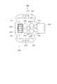
電子回路内蔵型モータ1は、モータ30、パワー部50、及び、制御部70を備えている。図1に示すように、電子回路内蔵型モータ1は、車両のステアリング91の回転軸たるコラム軸92に取り付けられたギア93を介しコラム軸92に回転トルクを発生させ、ステアリング91による操舵をアシストする。具体的には、ステアリング91が運転者によって操作されると、当該操作によってコラム軸92に生じる操舵トルクをトルクセンサ94によって検出し、また、車速情報をCAN(Controller Area Network)から取得して(不図示)、運転者のステアリング91による操舵をアシストする。もちろん、このような機構を利用すれば、制御手法によっては、操舵のアシストのみでなく、高速道路における車線キープ、駐車場における駐車スペースへの誘導など、ステアリング91の操作を自動制御することも可能である。  The electronic circuit built-inmotor 1 includes amotor 30, apower unit 50, and acontrol unit 70. As shown in FIG. 1, the electronic circuit built-inmotor 1 assists steering by the steering 91 by generating rotational torque on thecolumn shaft 92 via agear 93 attached to thecolumn shaft 92 that is a rotating shaft of the steering 91 of the vehicle. To do. Specifically, when thesteering wheel 91 is operated by the driver, a steering torque generated in thecolumn shaft 92 by the operation is detected by thetorque sensor 94, and vehicle speed information is acquired from a CAN (Controller Area Network) ( (Not shown), assisting the driver with thesteering wheel 91. Of course, if such a mechanism is used, depending on the control method, it is possible not only to assist the steering, but also to automatically control the operation of thesteering wheel 91 such as keeping the lane on the highway and guiding to the parking space on the parking lot. It is.

モータ30は、上記ギア93を正逆回転させるブラシレスモータである。このモータ30へ電力供給を行うのがパワー部50である。パワー部50は、電源51からの電源ラインに介在するチョークコイル52、シャント抵抗53、及び、二組のインバータ60,68を有している。  Themotor 30 is a brushless motor that rotates thegear 93 forward and backward. Thepower unit 50 supplies power to themotor 30. Thepower unit 50 includes achoke coil 52, ashunt resistor 53, and two sets ofinverters 60 and 68 interposed in a power supply line from thepower supply 51.

一方のインバータ60は、電界効果トランジスタの一種である7つのMOSFET(metal-oxide-semiconductor field-effect transistor )61、62、63、64、65、66、67で構成されている。これらMOSFET61〜67は、スイッチング素子である。具体的には、ゲートの電位により、ソース−ドレイン間がON(導通)またはOFF(遮断)される。なお、他方のインバータ68も、一方のインバータ60と同様の構成となっているため、以下、インバータ60についてのみ説明する。  Oneinverter 60 includes seven MOSFETs (metal-oxide-semiconductor field-effect transistors) 61, 62, 63, 64, 65, 66, and 67 which are a kind of field effect transistors. TheseMOSFETs 61 to 67 are switching elements. Specifically, the source and drain are turned on (conducted) or turned off (cut off) depending on the potential of the gate. Since theother inverter 68 has the same configuration as the oneinverter 60, only theinverter 60 will be described below.

以下、MOSFET61〜67を、単に、FET61〜67と記述する。なお、シャント抵抗53に最も近いFET67は、逆接保護のためのものである。すなわち、このFET67は、電源の誤接続がなされた場合に、逆向きの電流が流れないようにする。  Hereinafter, theMOSFETs 61 to 67 are simply referred to asFETs 61 to 67. TheFET 67 closest to theshunt resistor 53 is for protection against reverse connection. That is, theFET 67 prevents a reverse current from flowing when the power supply is erroneously connected.

ここで、残りの6つのFET61〜66の接続について説明しておく。
3つのFET61〜63のドレインが、電源ライン側に接続されている。また、FET61〜63のソースがそれぞれ、残り3つのFET64〜66のドレインに接続されている。さらにまた、これらのFET64〜66のソースがグランドに接続されている。また、6つのFET61〜66のゲートは、後述するプリドライバ71の6つの出力端子に接続されている。そして、図1中で上下ペアとなるFET61〜66同士の接続点がそれぞれ、モータ30のU相コイル、V相コイル、W相コイルに接続されている。
Here, the connection of the remaining sixFETs 61 to 66 will be described.
The drains of the threeFETs 61 to 63 are connected to the power supply line side. Further, the sources of theFETs 61 to 63 are connected to the drains of the remaining threeFETs 64 to 66, respectively. Furthermore, the sources of theseFETs 64 to 66 are connected to the ground. The gates of the sixFETs 61 to 66 are connected to six output terminals of a pre-driver 71 described later. 1 are connected to the U-phase coil, the V-phase coil, and the W-phase coil of themotor 30, respectively.

なお、FET61〜66を区別する必要があるときは、図1中の記号を用い、FET(Su+)61、FET(Sv+)62、FET(Sw+)63、FET(Su−)64、FET(Sv−)65、FET(Sw−)66と記述する。  When it is necessary to distinguish theFETs 61 to 66, the symbols in FIG. 1 are used, and the FET (Su +) 61, the FET (Sv +) 62, the FET (Sw +) 63, the FET (Su−) 64, and the FET (Sv -) 65 and FET (Sw-) 66.

また、FET(Su+)61の電源ラインとFET(Su−)64のグランドとの間には、アルミ電解コンデンサ54が並列に接続されている。同様に、FET(Sv+)62の電源ラインとFET(Sv−)65のグランドとの間にはアルミ電解コンデンサ55が並列に接続されており、FET(Sw+)63の電源ラインとFET(Sw−)66のグランドとの間にはアルミ電解コンデンサ56が並列に接続されている。以下、「アルミ電解コンデンサ」を単に「コンデンサ」と記述する。  An aluminumelectrolytic capacitor 54 is connected in parallel between the power supply line of the FET (Su +) 61 and the ground of the FET (Su−) 64. Similarly, an aluminumelectrolytic capacitor 55 is connected in parallel between the power supply line of the FET (Sv +) 62 and the ground of the FET (Sv−) 65, and the power supply line of the FET (Sw +) 63 and the FET (Sw−) are connected. The aluminumelectrolytic capacitor 56 is connected in parallel with the ground 66). Hereinafter, “aluminum electrolytic capacitor” is simply referred to as “capacitor”.

制御部70は、上記プリドライバ71、カスタムIC72、位置センサ73、及び、マイコン74を備えている。カスタムIC72は、機能ブロックとして、レギュレータ部75、位置センサ信号増幅部76、及び、検出電圧増幅部77を含む。  Thecontrol unit 70 includes the pre-driver 71,custom IC 72,position sensor 73, andmicrocomputer 74. Thecustom IC 72 includes aregulator unit 75, a position sensorsignal amplification unit 76, and a detectionvoltage amplification unit 77 as functional blocks.

レギュレータ部75は、電源を安定化する安定化回路である。このレギュレータ部75は、各部へ供給される電源の安定化を行う。例えばマイコン74は、このレギュレータ部75により、安定した所定電源電圧(例えば5V)で動作することになる。  Theregulator unit 75 is a stabilization circuit that stabilizes the power supply. Theregulator unit 75 stabilizes the power supplied to each unit. For example, themicrocomputer 74 is operated with a stable predetermined power supply voltage (for example, 5 V) by theregulator unit 75.

位置センサ信号増幅部76には、位置センサ73からの信号が入力される。位置センサ73は、後述するように、モータ30の回転位置信号を出力する。位置センサ信号増幅部76は、この回転位置信号を増幅してマイコン74へ出力する。
検出電圧増幅部77は、パワー部50に設けられたシャント抵抗53の両端電圧を検出し、当該両端電圧を増幅してマイコン74へ出力する。
A signal from theposition sensor 73 is input to the positionsensor signal amplifier 76. Theposition sensor 73 outputs a rotational position signal of themotor 30 as will be described later. The positionsensor signal amplifier 76 amplifies this rotational position signal and outputs it to themicrocomputer 74.
Thedetection voltage amplifier 77 detects the voltage across theshunt resistor 53 provided in thepower unit 50, amplifies the voltage across the both ends, and outputs the amplified voltage to themicrocomputer 74.

したがって、マイコン74には、モータ30の回転位置信号、及び、シャント抵抗53の両端電圧が入力される。また、マイコン74には、コラム軸92に取り付けられたトルクセンサ94から操舵トルク信号が入力される。さらにまた、マイコン74には、CANを経由して車速情報が入力される。  Therefore, the rotational position signal of themotor 30 and the voltage across theshunt resistor 53 are input to themicrocomputer 74. A steering torque signal is input to themicrocomputer 74 from atorque sensor 94 attached to thecolumn shaft 92. Furthermore, vehicle speed information is input to themicrocomputer 74 via the CAN.

これにより、マイコン74は、操舵トルク信号及び車速情報が入力されるとステアリング91による操舵を車速に応じてアシストするように、回転位置信号に合わせ、プリドライバ71を介し、インバータ60を制御する。インバータ60の制御は、具体的には、プリドライバ71を介したFET61〜66のON/OFFによって行う。つまり、6つのFET61〜66のゲートはプリドライバ71の6つの出力端子に接続されているため、プリドライバ71により、ゲート電位が変化させられる。  Thereby, themicrocomputer 74 controls theinverter 60 via the pre-driver 71 in accordance with the rotational position signal so that the steering by the steering 91 is assisted according to the vehicle speed when the steering torque signal and the vehicle speed information are input. Specifically, theinverter 60 is controlled by turning on / off theFETs 61 to 66 via thepre-driver 71. That is, since the gates of the sixFETs 61 to 66 are connected to the six output terminals of the pre-driver 71, the gate potential is changed by the pre-driver 71.

また、マイコン74は、検出電圧増幅部77から入力されるシャント抵抗53の両端電圧に基づき、モータ30へ供給する電流を正弦波に近づけるべくインバータ60を制御する。  Further, themicrocomputer 74 controls theinverter 60 so that the current supplied to themotor 30 approaches a sine wave based on the voltage across theshunt resistor 53 input from thedetection voltage amplifier 77.

このようなインバータ60の制御に際し、チョークコイル52は、電源51によるノイズを低減する。また、コンデンサ54〜56は、電荷を蓄えることで、FET61〜66への電力供給を補助したり、サージ電圧などのノイズ成分を抑制したりする。なお、逆接保護用のFET67が設けられているため、電源の誤接続があっても、コンデンサ54〜56が損傷することはない。  When theinverter 60 is controlled, thechoke coil 52 reduces noise caused by thepower source 51. Further, thecapacitors 54 to 56 accumulate electric charges, thereby assisting power supply to theFETs 61 to 66 and suppressing noise components such as a surge voltage. Since the reverseconnection protection FET 67 is provided, thecapacitors 54 to 56 are not damaged even if the power supply is erroneously connected.

ところで、このようにモータ30の駆動制御のためにはパワー部50及び制御部70が必要となる。これらのパワー部50及び制御部70が、いわゆるコントロールユニット(ECU)として構成されるのであるが、電子回路内蔵型モータ1は、このECUの内蔵構成に特徴を有する。  By the way, thepower unit 50 and thecontrol unit 70 are necessary for the drive control of themotor 30 as described above. Thepower unit 50 and thecontrol unit 70 are configured as a so-called control unit (ECU), but the electronic circuit built-inmotor 1 is characterized by a built-in configuration of the ECU.

なお、EPSに用いられるモータ30の出力は200W〜500W程度であり、電子回路内蔵型モータ1全体に占めるパワー部50及び制御部70の領域は、20〜40%程度となる。また、モータ30の出力が大きいため、パワー部50が大型化する傾向にあり、パワー部50及び制御部70の占める領域のうちの70%以上がパワー部50の占める領域となる。  In addition, the output of themotor 30 used for EPS is about 200W-500W, and the area | region of thepower part 50 and thecontrol part 70 which occupies for thewhole motor 1 with a built-in electronic circuit becomes about 20-40%. Moreover, since the output of themotor 30 is large, thepower unit 50 tends to increase in size, and 70% or more of the region occupied by thepower unit 50 and thecontrol unit 70 is the region occupied by thepower unit 50.

パワー部50を構成する部品で大きなものは、チョークコイル52、コンデンサ54〜56、そして、FET61〜67である。FET61〜67は、半導体モジュールとして構成される。  The major components constituting thepower unit 50 are achoke coil 52,capacitors 54 to 56, andFETs 61 to 67. TheFETs 61 to 67 are configured as semiconductor modules.

本形態では、FET(Su+)61、及び、FET(Su−)64が半導体チップとして構成されており、当該半導体チップが樹脂モールドされて一つの半導体モジュールとなっている。  In this embodiment, the FET (Su +) 61 and the FET (Su−) 64 are configured as semiconductor chips, and the semiconductor chip is resin-molded to form one semiconductor module.

また、FET(Sv+)62、及び、FET(Sv−)65が半導体チップとして構成されており、当該半導体チップが樹脂モールドされて一つの半導体モジュールとなっている。  Further, the FET (Sv +) 62 and the FET (Sv−) 65 are configured as a semiconductor chip, and the semiconductor chip is resin-molded to form one semiconductor module.

さらにまた、FET(Sw+)63、及び、FET(Sw−)66が半導体チップとして構成されており、当該半導体チップが樹脂モールドされて一つの半導体モジュールとなっている。  Furthermore, the FET (Sw +) 63 and the FET (Sw−) 66 are configured as semiconductor chips, and the semiconductor chip is resin-molded to form one semiconductor module.

なお、逆接保護用のFET67については後述する。
つまり、図1のインバータ60は、3つの半導体モジュールで構成される。本形態では、図1に示すように、計二組のインバータ60,68を備えている。これにより、一つのインバータ60,68に流れる電流を半分に減らしている。このように二組のインバータ60,68を備えることから、本形態では、6つの半導体モジュール、及び、6つのコンデンサを有することとなる。
The reverseconnection protection FET 67 will be described later.
That is, theinverter 60 in FIG. 1 is configured by three semiconductor modules. In this embodiment, as shown in FIG. 1, two sets ofinverters 60 and 68 are provided. As a result, the current flowing through oneinverter 60, 68 is reduced by half. Thus, since two sets ofinverters 60 and 68 are provided, in this embodiment, six semiconductor modules and six capacitors are provided.

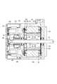
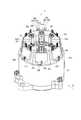
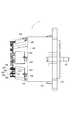
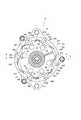
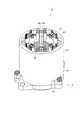
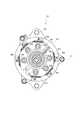
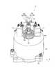
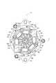
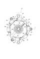
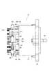
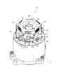
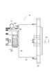
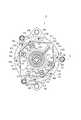
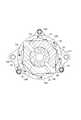
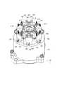
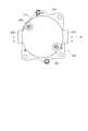
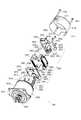
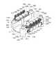
次に、本形態の電子回路内蔵型モータ1の構造について説明する。図2は電子回路内蔵型モータ1の平面図であり、図3は図2の矢印K方向に見た側面図であり、図4は図3のIV−IV線断面図であり、図5は斜視図であり、図6は分解斜視図である。  Next, the structure of the electronic circuit built-inmotor 1 of this embodiment will be described. 2 is a plan view of themotor 1 with built-in electronic circuit, FIG. 3 is a side view seen in the direction of arrow K in FIG. 2, FIG. 4 is a sectional view taken along line IV-IV in FIG. FIG. 6 is a perspective view, and FIG. 6 is an exploded perspective view.

最初に、図4に基づいて、電子回路内蔵型モータ1の可動部分の構造を説明しておく。
電子回路内蔵型モータ1は、その外郭として、円筒状のモータケース101と、モータケース101に対し出力端側に螺着されるフレームエンド102と、電子回路部分を覆う有底円筒状のカバー103とを備えている。
First, the structure of the movable part of the electronic circuit built-inmotor 1 will be described with reference to FIG.
Themotor 1 with a built-in electronic circuit includes acylindrical motor case 101, aframe end 102 screwed to themotor case 101 on the output end side, and a bottomedcylindrical cover 103 that covers the electronic circuit portion. And.

ここでモータ30は、モータケース101と、モータケース101の径方向内側に配置されたステータ201と、ステータ201の径方向内側に配置されたロータ301と、ロータ301と共に回転するシャフト401とを有している。  Here, themotor 30 includes amotor case 101, astator 201 disposed radially inward of themotor case 101, arotor 301 disposed radially inward of thestator 201, and ashaft 401 that rotates together with therotor 301. doing.

ステータ201は、モータケース101の径内方向に突出する12個の突極202を有している。この突極202は、モータケース101の周方向に所定間隔で設けられている。突極202は、磁性材料の薄板を積層してなる積層鉄心203と、積層鉄心203の軸方向外側に嵌合するインシュレータ204とを有している。このインシュレータ204には、巻線205が巻回されている。巻線205へ電流を供給するための取出線206は、巻線205の6箇所から引き出されている。巻線205は、取出線206への電流供給の態様によって、U相、V相、及び、W相の三相巻線として機能する。この意味で、巻線205が、U相、V相、及び、W相の三相巻線を構成している。取出線206は、モータケース101の軸方向端部に設けられた6つの穴から電子回路側へ引き出されている。  Thestator 201 has twelve salient poles 202 that protrude in the radial inner direction of themotor case 101. The salient poles 202 are provided at predetermined intervals in the circumferential direction of themotor case 101. The salient pole 202 has alaminated iron core 203 formed by laminating thin plates of magnetic material, and an insulator 204 fitted to the outside of thelaminated iron core 203 in the axial direction. A winding 205 is wound around the insulator 204. Leadwires 206 for supplying current to the winding 205 are drawn from six locations of the winding 205. The winding 205 functions as a U-phase, V-phase, and W-phase three-phase winding depending on the manner of current supply to the lead-outline 206. In this sense, the winding 205 constitutes a U-phase, V-phase, and W-phase three-phase winding. The lead-outline 206 is led out to the electronic circuit side from six holes provided at the axial end of themotor case 101.

ロータ301は、例えば鉄等の磁性体から筒状に形成されている。ロータ301は、ロータコア302と、当該ロータコア302の径方向外側に設けられた永久磁石303とを有している。永久磁石303は、N極とS極とを周方向に交互に有している。  Therotor 301 is formed in a cylindrical shape from a magnetic material such as iron. Therotor 301 includes arotor core 302 and apermanent magnet 303 provided on the outer side in the radial direction of therotor core 302. Thepermanent magnet 303 has N poles and S poles alternately in the circumferential direction.

シャフト401は、ロータコア302の軸中心に形成された軸穴304に固定されている。また、シャフト401は、モータケース101の軸受け104と、フレームエンド102に設けられた軸受け105とによって、回転可能に軸支されている。これにより、シャフト401は、ステータ201に対し、ロータ301と共に回転可能となっている。なお、軸受け104が設けられる部分は、電子回路(駆動制御部)とモータ(可動部)との境界であり、以下では、この境界壁部分を、モータケース101の端部106と称する。さらにまた、シャフト401は、端部106から電子回路側へ延び、電子回路側の先端に、回転位置を検出するためのマグネット402を有している。シャフト401の電子回路側の先端付近には、樹脂製のプリント基板801が配置される。このプリント基板801は、その中央に、位置センサ73(図4中には不図示、図1参照)を有している。これにより、マグネット402の回転位置、すなわちシャフト401の回転位置が、位置センサ73によって検出される。  Theshaft 401 is fixed to ashaft hole 304 formed at the center of therotor core 302. Theshaft 401 is rotatably supported by a bearing 104 of themotor case 101 and abearing 105 provided at theframe end 102. Thereby, theshaft 401 can rotate with therotor 301 with respect to thestator 201. The portion where thebearing 104 is provided is a boundary between the electronic circuit (drive control unit) and the motor (movable unit). Hereinafter, this boundary wall portion is referred to as anend portion 106 of themotor case 101. Furthermore, theshaft 401 extends from theend portion 106 to the electronic circuit side, and has amagnet 402 for detecting the rotational position at the tip of the electronic circuit side. A resin printedboard 801 is disposed near the tip of theshaft 401 on the electronic circuit side. The printedcircuit board 801 has a position sensor 73 (not shown in FIG. 4, refer to FIG. 1) in the center thereof. Thereby, the rotational position of themagnet 402, that is, the rotational position of theshaft 401 is detected by theposition sensor 73.

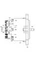
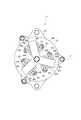
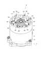
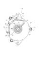
次に、図2〜図6を参照しつつ、電子回路の構造を説明する。なお、図2、図3及び図5では、カバー103及びプリント基板801を省略して示している。また、ここでは、最初にパワー部50の構成について説明し、次に、制御部70の構成について説明する。  Next, the structure of the electronic circuit will be described with reference to FIGS. 2, 3, and 5, thecover 103 and the printedboard 801 are omitted. Here, the configuration of thepower unit 50 will be described first, and then the configuration of thecontrol unit 70 will be described.

パワー部50のインバータ60を構成する7つのFET61〜67(図1参照)が3つの半導体モジュールとして構成されることは既に述べた。そして、本形態の電子回路内蔵型モータ1は、インバータ60を二組備えているため、6つの半導体モジュールを備えていることも既に述べた通りである。  As described above, the sevenFETs 61 to 67 (see FIG. 1) constituting theinverter 60 of thepower unit 50 are configured as three semiconductor modules. Since the electronic circuit built-inmotor 1 of this embodiment includes two sets ofinverters 60, as described above, it includes six semiconductor modules.

すなわち、図2に示すように、電子回路内蔵型モータ1は、6つの半導体モジュール501、502、503、504、505、506を備えている。これら半導体モジュール501〜506を区別する場合、図2中の記号を用い、U1半導体モジュール501、V1半導体モジュール502、W1半導体モジュール503、U2半導体モジュール504、V2半導体モジュール505、W2半導体モジュール506と記述することとする。  That is, as shown in FIG. 2, the electronic circuit built-inmotor 1 includes sixsemiconductor modules 501, 502, 503, 504, 505, and 506. When thesemiconductor modules 501 to 506 are distinguished, the symbols in FIG. 2 are used to describe theU1 semiconductor module 501, theV1 semiconductor module 502, theW1 semiconductor module 503, theU2 semiconductor module 504, theV2 semiconductor module 505, and theW2 semiconductor module 506. I decided to.

図1との対応関係について言及すれば、U1半導体モジュール501が、U相に対応するFET61、64を有している。また、V1半導体モジュール502が、V相に対応するFET62、65を有している。さらにまた、W1半導体モジュールが、W相に対応するFET63、66及び逆接保護用のFET67を有している。同様に、U2半導体モジュール504がU相に対応するFET61、64及び逆接保護用のFET67を有し、V2半導体モジュール505がV相に対応するFET62、65を有し、W2半導体モジュール506がW相に対応するFET63、66を有している。すなわち、U1、V1、W1の3つの半導体モジュール501〜503によって一組のインバータ60が構成されており、U2、V2、W2の3つの半導体モジュール504〜506によってもう一組のインバータ60が構成されている。  Referring to the correspondence relationship with FIG. 1, theU1 semiconductor module 501 has FETs 61 and 64 corresponding to the U phase. Further, theV1 semiconductor module 502 includesFETs 62 and 65 corresponding to the V phase. Furthermore, the W1 semiconductor module hasFETs 63 and 66 corresponding to the W phase and anFET 67 for reverse connection protection. Similarly, theU2 semiconductor module 504 has FETs 61 and 64 corresponding to the U phase and theFET 67 for reverse connection protection, theV2 semiconductor module 505 has FETs 62 and 65 corresponding to the V phase, and theW2 semiconductor module 506 has the W phase.FETs 63 and 66 corresponding to. That is, one set ofinverters 60 is configured by the three semiconductor modules 501-503 of U1, V1, and W1, and another set ofinverters 60 is configured by the three semiconductor modules 504-506 of U2, V2, and W2. ing.

これらインバータ60を構成するU1〜W1の3つの半導体モジュール501〜503、及び、U2〜W2の3つの半導体モジュール504〜506は、バスバー507で連結されてモジュールユニットを形成している。バスバー507は、連結機能を有すると共に、モータケース101に対し遠い側のバスバー507aがグランドを兼ね、モータケース101に近い側のバスバー507bが電源ラインを兼ねる(図5参照)。すなわち、バスバー507を経由して半導体モジュール501〜506へ電力が供給される。  The threesemiconductor modules 501 to 503 U1 to W1 and the threesemiconductor modules 504 to 506 U2 to W2 constituting theinverter 60 are connected by abus bar 507 to form a module unit. Thebus bar 507 has a connecting function, and thebus bar 507a far from themotor case 101 also serves as a ground, and thebus bar 507b closer to themotor case 101 serves as a power supply line (see FIG. 5). That is, electric power is supplied to thesemiconductor modules 501 to 506 via thebus bar 507.

なお、図2〜図6は、半導体モジュール501〜506等の組み付け構造を示すものであり、電力供給構造については図示していない。この点、実際には、カバー103にコネクタが取り付けられ、そのコネクタを経由してバスバー507へ電力が供給される。  2 to 6 show the assembly structure of thesemiconductor modules 501 to 506 and the like, and the power supply structure is not shown. In this respect, a connector is actually attached to thecover 103, and power is supplied to thebus bar 507 via the connector.

次に、半導体モジュール501〜506の配置について説明する。
半導体モジュール501〜506は、モータケース101の端部106からシャフト401の中心線方向と同方向へ延設されたヒートシンク601に対し取り付けられている。
Next, the arrangement of thesemiconductor modules 501 to 506 will be described.
Thesemiconductor modules 501 to 506 are attached to aheat sink 601 extending from theend portion 106 of themotor case 101 in the same direction as the center line direction of theshaft 401.

そこでヒートシンク601について説明しておく。
ヒートシンク601は、図2に示すように、軸方向に垂直な断面における形状が略台形状の2つの柱状部材がシャフト401の中心線を挟むよう並べられ、さらに、中心に円柱形状の空間が形成されるように所定半径部分を切り欠いた形状となっている。言い換えれば、ヒートシンク601は、全体として見ると、厚肉の軸方向視八角形状の筒形状とも言える。もちろん、八角形状には限定されず、例えば軸方向視六角形状としてもよい。ヒートシンク601は軸方向断面視略台形状の柱状部材を構成する側壁602を有し、この側壁602には、不連続部分を構成する切り欠き部603、604が設けられている。ここで、ヒートシンク601は、モータケース101と一体成形されている。
Therefore, theheat sink 601 will be described.
As shown in FIG. 2, theheat sink 601 is arranged such that two columnar members having a substantially trapezoidal shape in a cross section perpendicular to the axial direction sandwich the center line of theshaft 401, and a cylindrical space is formed at the center. As shown, the predetermined radius portion is cut out. In other words, theheat sink 601 can be said to be a thick-walled octagonal cylindrical shape when viewed as a whole. Of course, the shape is not limited to the octagonal shape, and may be a hexagonal shape as viewed in the axial direction, for example. Theheat sink 601 has aside wall 602 that constitutes a columnar member having a substantially trapezoidal shape in a sectional view in the axial direction, and theside wall 602 is provided withnotches 603 and 604 that constitute discontinuous portions. Here, theheat sink 601 is integrally formed with themotor case 101.

また、ヒートシンク601の側壁602は、径外方向へ向く側面のうち切り欠き部603、604に隣接する側面よりも幅広に形成された側壁面605を有している。側壁面605は、円周方向に計6つ形成されている。各側壁面605の径内方向には、中心の円柱形状の空間に開口する収容部606が形成されている。この収容部606は、コンデンサの外形に合わせた円弧面を有している。また、収容部606は、側壁面605に対応する位置に形成されている。ヒートシンク601において、収容部606が形成された部位は薄肉となっているが、収容部606からモータケース101の端部106までの間は、収容部606が設けられていない部分と同様に肉厚の厚肉部107となっている(図4参照)。  Further, theside wall 602 of theheat sink 601 has aside wall surface 605 formed wider than the side surface adjacent to thenotches 603 and 604 among the side surfaces facing radially outward. A total of six side wall surfaces 605 are formed in the circumferential direction. In the radially inward direction of eachside wall surface 605, ahousing portion 606 that opens into a central cylindrical space is formed. Thehousing portion 606 has an arc surface that matches the outer shape of the capacitor. Further, theaccommodating portion 606 is formed at a position corresponding to theside wall surface 605. In theheat sink 601, the portion where thehousing portion 606 is formed is thin, but the portion between thehousing portion 606 and theend portion 106 of themotor case 101 is as thick as the portion where thehousing portion 606 is not provided. The thick portion 107 (see FIG. 4).

以上のように形成されたヒートシンク601に対し、半導体モジュール501〜506は、径外方向を向く側壁面605に一つずつ配置されている。半導体モジュール501〜506は、モールドされた半導体チップの面の方向に広がる板状であり、相対的に面積の大きな面の一方が放熱面となっている(以下の形態でも同様)。例えば、放熱面には、銅などの金属が露出しているという具合である。半導体モジュール501〜506は、その放熱面が側壁面605に接触するように配置されている。このとき、側壁面605は平面で構成されており、これに合わせて、半導体モジュール501〜506の放熱面も平面となっている。なお、半導体モジュール501〜506の放熱面とヒートシンク601の側壁面605との間に絶縁シートを介在させる構成であってもよい。この点については、以下の形態でも同様である。  With respect to theheat sink 601 formed as described above, thesemiconductor modules 501 to 506 are arranged one by one on theside wall surface 605 facing the radially outward direction. Thesemiconductor modules 501 to 506 have a plate shape extending in the direction of the surface of the molded semiconductor chip, and one of the surfaces having a relatively large area is a heat dissipation surface (the same applies to the following embodiments). For example, a metal such as copper is exposed on the heat dissipation surface. Thesemiconductor modules 501 to 506 are arranged such that their heat dissipation surfaces are in contact with the side wall surfaces 605. At this time, theside wall surface 605 is a flat surface, and the heat radiation surfaces of thesemiconductor modules 501 to 506 are also flat according to this. Note that an insulating sheet may be interposed between the heat radiation surfaces of thesemiconductor modules 501 to 506 and theside wall surface 605 of theheat sink 601. This also applies to the following embodiments.

半導体モジュール501〜506は、上述のごとくヒートシンク601の側壁面605に配置されることで、半導体チップ面の垂線がシャフト401の中心線に垂直となっている(図5参照)。すなわち、本形態において半導体モジュール501〜506は、縦配置されている。  Thesemiconductor modules 501 to 506 are arranged on theside wall surface 605 of theheat sink 601 as described above, so that the perpendicular of the semiconductor chip surface is perpendicular to the center line of the shaft 401 (see FIG. 5). That is, in this embodiment, thesemiconductor modules 501 to 506 are arranged vertically.

半導体モジュール501〜506は、モータケース101側の端部に、巻線用端子508を有している(図3等参照)。この巻線用端子508は、径方向外側へ折り曲げられて形成されている。巻線205へ電流を供給するための取出線206がモータケース101の端部106に設けられた6つの穴から電子回路側へ引き出されていることは上述したが、この取出線206は、半導体モジュール501〜506の径方向外側の空間に引き出されている。これにより、取出線206と巻線用端子508とは、半導体モジュール501〜506の径方向外側の空間において、取出線206が巻線用端子508に挟持されるようにして、電気的に接続されている。  Thesemiconductor modules 501 to 506 have a windingterminal 508 at the end on themotor case 101 side (see FIG. 3 and the like). The windingterminal 508 is formed to be bent outward in the radial direction. As described above, the lead-outline 206 for supplying current to the winding 205 is led out from the six holes provided in theend portion 106 of themotor case 101 to the electronic circuit side. Themodules 501 to 506 are drawn out to the space outside in the radial direction. As a result, the lead-outline 206 and the windingterminal 508 are electrically connected so that the lead-outline 206 is sandwiched between the windingterminals 508 in the radially outer space of thesemiconductor modules 501 to 506. ing.

また、半導体モジュール501〜506は、反モータケース101側の端部に、6本の制御用端子509と、2本のコンデンサ用端子510とを有している。制御用端子509は、プリント基板801(図4参照)のスルーホールに挿通した状態で半田付けされる。これにより、半導体モジュール501〜506が、制御部70(図1参照)に電気的に接続される。一方、コンデンサ用端子510はそれぞれ、半導体モジュール501〜506の内部で電源ライン及びグランドから分岐している。そして、いずれのコンデンサ用端子510も、径内方向へ折り曲げられている。このようにプリント基板801は、ヒートシンク601の先端部とカバー103との間にできる離間スペースに配置される。  Further, thesemiconductor modules 501 to 506 have sixcontrol terminals 509 and twocapacitor terminals 510 at the end on the side opposite to themotor case 101. Thecontrol terminal 509 is soldered in a state of being inserted through the through hole of the printed circuit board 801 (see FIG. 4). Thereby, thesemiconductor modules 501 to 506 are electrically connected to the control unit 70 (see FIG. 1). On the other hand, thecapacitor terminal 510 branches from the power supply line and the ground inside thesemiconductor modules 501 to 506, respectively. Eachcapacitor terminal 510 is bent in the radially inward direction. In this way, the printedcircuit board 801 is disposed in a space that is formed between the tip of theheat sink 601 and thecover 103.

図2等に示すように、半導体モジュール501〜506に対し、ヒートシンク601と同じ側に、つまり径方向内側に、6つのコンデンサ701、702、703、704、705、706が配置されている。これらコンデンサ701〜706を区別するため、図2中の記号を用い、U1コンデンサ701、V1コンデンサ702、W1コンデンサ703、U2コンデンサ704、V2コンデンサ705、W2コンデンサ706と記述する。  As shown in FIG. 2 and the like, sixcapacitors 701, 702, 703, 704, 705, and 706 are arranged on the same side as theheat sink 601 with respect to thesemiconductor modules 501 to 506, that is, radially inward. In order to distinguish thesecapacitors 701 to 706, the symbols in FIG. 2 are used to describe the capacitors asU1 capacitor 701,V1 capacitor 702,W1 capacitor 703,U2 capacitor 704,V2 capacitor 705, andW2 capacitor 706.

図1との対応関係について言及すれば、U1コンデンサ701がコンデンサ54に対応する。また、V1コンデンサ702がコンデンサ55に対応する。さらにまた、W1コンデンサ703がコンデンサ56に対応する。同様に、U2コンデンサ704がコンデンサ54に対応し、V2コンデンサ705がコンデンサ55に対応し、W2コンデンサ706がコンデンサ56に対応する。  Referring to the correspondence relationship with FIG. 1, theU1 capacitor 701 corresponds to thecapacitor 54. AV1 capacitor 702 corresponds to thecapacitor 55. Furthermore, theW1 capacitor 703 corresponds to thecapacitor 56. Similarly, theU2 capacitor 704 corresponds to thecapacitor 54, theV2 capacitor 705 corresponds to thecapacitor 55, and theW2 capacitor 706 corresponds to thecapacitor 56.

コンデンサ701〜706は、ヒートシンク601の収容部606に収容されて半導体モジュール501〜506に対して一つずつ、半導体モジュール501〜506の近傍に配置されている。コンデンサ701〜706は円柱形状を呈し、その軸がシャフト401の中心線に平行となるように配置されている(図5参照)。また、半導体モジュール501〜506の有するコンデンサ用端子510が径内方向へ折り曲げられていることで、この折り曲げられたコンデンサ用端子510に対し、コンデンサ701〜706の端子が、直接的に接続されている。  Thecapacitors 701 to 706 are accommodated in theaccommodating portion 606 of theheat sink 601 and are arranged near thesemiconductor modules 501 to 506 one by one with respect to thesemiconductor modules 501 to 506. Thecapacitors 701 to 706 have a cylindrical shape, and are arranged so that the axis thereof is parallel to the center line of the shaft 401 (see FIG. 5). In addition, since thecapacitor terminals 510 included in thesemiconductor modules 501 to 506 are bent inwardly, the terminals of thecapacitors 701 to 706 are directly connected to thebent capacitor terminals 510. Yes.

また、シャフト401が電子回路側へ延びていることは既に述べたが、図4等に示すように、このシャフト401が貫通した状態で、チョークコイル52が配置されている。チョークコイル52は、ヒートシンク601の中心に形成された円柱形状の空間に配置されている。チョークコイル52はドーナツ状の鉄心にコイル線が巻回されてなり、コイル端は、ヒートシンク601の一方の切り欠き部603を通って、径外方向へ引き出されている(図2参照)。  As described above, theshaft 401 extends to the electronic circuit side. As shown in FIG. 4 and the like, thechoke coil 52 is disposed with theshaft 401 penetrating. Thechoke coil 52 is disposed in a cylindrical space formed at the center of theheat sink 601. Thechoke coil 52 is formed by winding a coil wire around a donut-shaped iron core, and the end of the coil passes through onecutout portion 603 of theheat sink 601 and is drawn outward (see FIG. 2).

なお、チョークコイル52のコイル端は電源ラインに介在するように接続されるが(図1参照)、図2〜図6は、チョークコイル52に対する電力供給構造については、図示していない。  In addition, although the coil end of thechoke coil 52 is connected so as to be interposed in the power supply line (see FIG. 1), the power supply structure for thechoke coil 52 is not shown in FIGS.

このように、径方向外側から径方向内側へ向かって、巻線用端子508と取出線206との接続部、半導体モジュール501〜506、ヒートシンク601、コンデンサ701〜706、チョークコイル52の順で配置され、径方向の空間が有効に活用されている。
次に、制御部70について説明する。制御部70は、図4等に示すプリント基板801上に形成される。すなわち、プリント基板801には、エッチング処理等により配線パターンが形成され、ここに制御部70を構成するICなどが実装される(IC等の部品は不図示)。
Thus, from the radially outer side to the radially inner side, the connection portion between the windingterminal 508 and thelead wire 206, thesemiconductor modules 501 to 506, theheat sink 601, thecapacitors 701 to 706, and thechoke coil 52 are arranged in this order. The radial space is effectively utilized.
Next, thecontrol unit 70 will be described. Thecontrol unit 70 is formed on a printedboard 801 shown in FIG. That is, a wiring pattern is formed on the printedcircuit board 801 by an etching process or the like, and an IC or the like constituting thecontrol unit 70 is mounted thereon (components such as an IC are not shown).

次に、本形態の電子回路内蔵型モータ1が発揮する効果について説明する。なお、以下では種々の効果を羅列するため、項番をつけて記載する。
(1)本形態の電子回路内蔵型モータ1では、半導体モジュール501〜506がシャフト401の中心線方向に配置されている。これにより、径方向の体格を小さくすることができる。また、半導体モジュール501〜506を縦配置とし、ヒートシンク601の側壁面605に接触させて配置した。さらにまた、ヒートシンク601に収容部606を設け、径方向に6つのコンデンサ701〜706を配置した。すなわち、6つの半導体モジュール501〜506の径内方向にヒートシンク601及びコンデンサ701〜706を配置した。これによって、従来の構成と異なり、軸方向の体格をも小さくすることができる。その結果、電子回路内蔵型モータ1の体格を可及的に小さくすることができる。
Next, the effect which themotor 1 with a built-in electronic circuit of this form exhibits is demonstrated. In the following, in order to list various effects, item numbers are used for description.
(1) In the electronic circuit built-inmotor 1 of this embodiment, thesemiconductor modules 501 to 506 are arranged in the center line direction of theshaft 401. Thereby, the physique of radial direction can be made small. Further, thesemiconductor modules 501 to 506 are arranged vertically and are placed in contact with theside wall surface 605 of theheat sink 601. Furthermore, thehousing portion 606 is provided in theheat sink 601, and sixcapacitors 701 to 706 are arranged in the radial direction. That is, theheat sink 601 and thecapacitors 701 to 706 are arranged in the radial direction of the sixsemiconductor modules 501 to 506. Thereby, unlike the conventional configuration, the physique in the axial direction can be reduced. As a result, the size of the electronic circuit built-inmotor 1 can be made as small as possible.

EPSに用いられるモータは、図7に示すように発展してきている。すなわち、モータとECUとが別体である「機電別体」の当初の構成から、配線等の取り回しをなくした「機電合体」が主流となっている。しかし、この「機電合体」は、ECUが直方体形状のケースに入れられており、モータケースの外側にECUを装着した形式であった。これをなるべくモータシルエット内に収めるという思想が「機電一体」の思想であるが、この場合、軸方向の体格が大きくなってしまうという問題があった。この点、本形態の電子回路内蔵型モータ1では、半導体モジュール501〜506を縦配置とするだけでなく、これによって確保されるスペースを利用することにより、コンデンサ701〜706との配置関係を工夫している。つまり、本形態の電子回路内蔵型モータ1は、各部品の配置関係の連関をその思想とする点において、「機電一体」を超える「機電融合」と言い得る。  Motors used in EPS have been developed as shown in FIG. That is, from the initial configuration of the “mechanical separate body” in which the motor and the ECU are separate bodies, the “mechanical combined body” that eliminates wiring and the like has become the mainstream. However, the “mechanical union” is a type in which the ECU is placed in a rectangular parallelepiped case and the ECU is mounted on the outside of the motor case. The idea of putting this in the motor silhouette as much as possible is the idea of “mechanical integration”, but in this case, there is a problem that the physique in the axial direction becomes large. In this regard, in the electronic circuit built-inmotor 1 of this embodiment, not only thesemiconductor modules 501 to 506 are vertically arranged, but also the arrangement relationship with thecapacitors 701 to 706 is devised by utilizing the space secured by this. doing. That is, the electronic circuit built-intype motor 1 of this embodiment can be said to be “mechanical fusion” that exceeds “mechanical integration” in that the relationship of the arrangement relation of each component is the concept.

(2)また、本形態の電子回路内蔵型モータ1では、半導体モジュール501〜506の半導体チップ面の垂線がシャフト401の中心線に垂直となっている。これにより、径方向のスペース確保に一層寄与する。  (2) Moreover, in the electronic circuit built-intype motor 1 of this embodiment, the perpendicular of the semiconductor chip surface of thesemiconductor modules 501 to 506 is perpendicular to the center line of theshaft 401. This further contributes to securing the radial space.

(3)さらにまた、本形態の電子回路内蔵型モータ1では、コンデンサ701〜706が半導体モジュール501〜506の近傍に配置されている。しかも、半導体モジュール501〜506がコンデンサ用の専用端子であるコンデンサ用端子510を有しており、コンデンサ701〜706は、その端子がコンデンサ用端子510に、基板を介することなく直接接続されている。これにより、基板を介して半導体モジュール501〜506とコンデンサ701〜706とを接続する場合と比較して、半導体モジュール501〜506とコンデンサ701〜706との配線を極力短くすることができ、コンデンサ701〜706の機能を十分に発揮させることができる。また、各半導体モジュール501〜506に対し一つずつコンデンサ701〜706を配置する構成であるため、各コンデンサ701〜706の容量を比較的小さくすることができ、コンデンサ701〜706自体の体格を抑えることができる。  (3) Furthermore, in the electronic circuit built-intype motor 1 of this embodiment, thecapacitors 701 to 706 are arranged in the vicinity of thesemiconductor modules 501 to 506. In addition, thesemiconductor modules 501 to 506 havecapacitor terminals 510 that are dedicated terminals for capacitors, and thecapacitors 701 to 706 are directly connected to thecapacitor terminals 510 without a substrate. . Thereby, compared with the case where thesemiconductor modules 501 to 506 and thecapacitors 701 to 706 are connected via the substrate, the wiring between thesemiconductor modules 501 to 506 and thecapacitors 701 to 706 can be shortened as much as possible. The function of ˜706 can be sufficiently exhibited. Moreover, since it is the structure which arrange | positions the capacitor | condensers 701-706 to each semiconductor module 501-506, the capacity | capacitance of each capacitor | condenser 701-706 can be made comparatively small, and the physique of capacitor | condenser 701-706 itself is suppressed. be able to.

(4)また、本形態の電子回路内蔵型モータ1では、シャフト401の中心線方向と同方向へモータケース101の端部106から延設されたヒートシンク601を有している。半導体モジュール501〜506は、このヒートシンク601の側壁602に配置される。これにより、半導体モジュール501〜506からの放熱が促進され、モータ30に大電流が流れるような電動アシスト装置へも容易に適用することができる。  (4) Further, the electronic circuit built-inmotor 1 of this embodiment includes theheat sink 601 extending from theend portion 106 of themotor case 101 in the same direction as the center line direction of theshaft 401. Thesemiconductor modules 501 to 506 are disposed on theside wall 602 of theheat sink 601. Thereby, the heat radiation from thesemiconductor modules 501 to 506 is promoted, and it can be easily applied to an electric assist device in which a large current flows through themotor 30.

(5)さらにまた、本形態の電子回路内蔵型モータ1では、半導体モジュール501〜506に対しヒートシンク601と同じ側にコンデンサ701〜706が配置されている。具体的には、ヒートシンク601に形成された収容部606にコンデンサ701〜706が収容されている。これにより、半導体モジュール501〜506の径外方向にスペースが確保できる。結果として、配線の取り回しなどが容易になる。  (5) Furthermore, in the electronic circuit built-intype motor 1 of this embodiment,capacitors 701 to 706 are arranged on the same side as theheat sink 601 with respect to thesemiconductor modules 501 to 506. Specifically,capacitors 701 to 706 are accommodated in anaccommodating portion 606 formed in theheat sink 601. Thereby, a space can be secured in the radially outward direction of thesemiconductor modules 501 to 506. As a result, wiring can be easily handled.

(6)また、本形態の電子回路内蔵型モータ1では、半導体モジュール501〜506の放熱面がヒートシンク601の側壁面605に接触するように配置されている。これにより、半導体モジュール501〜506からの放熱を一層促進させることができる。
(7)また、側壁面605が平面であるため、半導体モジュール501〜506の放熱面も平面となっている。この点、半導体モジュール501〜506側の平面加工の容易性という観点から有利である。
(6) Further, in the electronic circuit built-intype motor 1 of this embodiment, the heat radiation surfaces of thesemiconductor modules 501 to 506 are disposed so as to contact theside wall surface 605 of theheat sink 601. Thereby, the heat radiation from thesemiconductor modules 501 to 506 can be further promoted.
(7) Since theside wall surface 605 is a flat surface, the heat radiation surfaces of thesemiconductor modules 501 to 506 are also flat. This is advantageous from the viewpoint of easy planar processing on thesemiconductor modules 501 to 506 side.

(8)さらにまた、本形態の電子回路内蔵型モータ1では、ヒートシンク601が、シャフト401の中心線の周りに側壁602を有している。そして、チョークコイル52が、側壁602の径方向内側に配置されている。これにより、体格の比較的大きなチョークコイル52を使用する場合でも、電子回路内蔵型モータ1の体格を可及的に小さくすることができる。
(9)また、側壁602には、不連続部分を構成する2つの切り欠き部603、604が設けられている。そして、一方の切り欠き部603を利用して、チョークコイル52のコイル端が径外方向へ取り出される。これにより、チョークコイル52の配線の取り回しが容易になっている。
(8) Furthermore, in the electronic circuit built-intype motor 1 of this embodiment, theheat sink 601 has aside wall 602 around the center line of theshaft 401. Thechoke coil 52 is disposed on the radially inner side of theside wall 602. Thereby, even when using thechoke coil 52 having a relatively large physique, the physique of the electronic circuit built-inmotor 1 can be made as small as possible.
(9) Further, theside wall 602 is provided with twonotches 603 and 604 that constitute discontinuous portions. And the coil end of thechoke coil 52 is taken out radially outward using onenotch 603. This facilitates the wiring of thechoke coil 52.

(10)また、本形態の電子回路内蔵型モータ1では、半導体モジュール501〜506とプリント基板801とが軸方向に並べて配置されている。半導体モジュール501〜506は制御用端子509を備えており、これらの制御用端子509がプリント基板801に半田付けされる。これにより、制御部70が半導体モジュール501〜506から配置上独立する構成であっても、電気的な接続は制御用端子509によって行えるため、構成が複雑になることがない。  (10) Moreover, in the electronic circuit built-inmotor 1 of this embodiment, thesemiconductor modules 501 to 506 and the printedcircuit board 801 are arranged side by side in the axial direction. Thesemiconductor modules 501 to 506 are provided withcontrol terminals 509, and thesecontrol terminals 509 are soldered to the printedcircuit board 801. As a result, even if thecontrol unit 70 has a configuration that is independent of thesemiconductor modules 501 to 506 in terms of arrangement, the electrical connection can be made by thecontrol terminal 509, so that the configuration is not complicated.

(11)さらにまた、本形態の電子回路内蔵型モータ1では、半導体モジュール501〜506がプリント基板801とは反対側の他端側に巻線用端子508を有している。そして、巻線用端子508が、取出線206に電気的に接続される。これにより、ステータ201の巻線205への電気的な接続を比較的容易に実現できる。  (11) Furthermore, in the electronic circuit built-intype motor 1 of this embodiment, thesemiconductor modules 501 to 506 have a windingterminal 508 on the other end side opposite to the printedboard 801. The windingterminal 508 is electrically connected to the lead-outline 206. Thereby, electrical connection to the winding 205 of thestator 201 can be realized relatively easily.

(12)また、本形態の電子回路内蔵型モータ1では、シャフト401の先端にマグネット402が設けられており、このマグネット402の回転位置をプリント基板801上の位置センサ73が検出することでシャフト401の回転位置が検出される。これにより、比較的簡単にモータ30の回転位置検出を行うことができる。  (12) Further, in the electronic circuit built-inmotor 1 of this embodiment, themagnet 402 is provided at the tip of theshaft 401, and theposition sensor 73 on the printedcircuit board 801 detects the rotational position of themagnet 402 so that the shaft Therotational position 401 is detected. Thereby, the rotational position of themotor 30 can be detected relatively easily.

(13)また、本形態の電子回路内蔵型モータ1では、W1及びU2の半導体モジュール503、504が逆接保護用のFET67を有している。これにより、電源の誤接続があった場合でも、コンデンサ701〜706の損傷を防止することができる。  (13) Also, in the electronic circuit built-inmotor 1 of this embodiment, the W1 andU2 semiconductor modules 503 and 504 have theFET 67 for reverse connection protection. Thereby, even when the power supply is erroneously connected, thecapacitors 701 to 706 can be prevented from being damaged.

(14)さらにまた、本形態の電子回路内蔵型モータ1では、U相、V相、W相の三相のそれぞれに半導体モジュール501〜506が対応している。具体的に、U相に対してはU1及びU2の半導体モジュール501、504が対応し、V相に対してはV1及びV2の半導体モジュール502、505が対応し、W相に対してはW1及びW2の半導体モジュール503、506が対応している。さらに、U1〜W1の半導体モジュール501〜503及びU2〜W2の半導体モジュール504〜506がそれぞれ、バスバー507で連結されてモジュールユニットを構成している。このように半導体モジュール501〜506が機能単位でモジュール化されているため、インバータ60の構成が簡単になる。  (14) Furthermore, in the electronic circuit built-inmotor 1 of this embodiment, thesemiconductor modules 501 to 506 correspond to the three phases of the U phase, the V phase, and the W phase, respectively. Specifically, U1 andU2 semiconductor modules 501 and 504 correspond to the U phase, V1 andV2 semiconductor modules 502 and 505 correspond to the V phase, and W1 and V2 correspond to the W phase. Thesemiconductor modules 503 and 506 of W2 correspond. Furthermore, U1-W1 semiconductor modules 501 to 503 and U2-W2 semiconductor modules 504 to 506 are respectively connected by abus bar 507 to constitute a module unit. Thus, since thesemiconductor modules 501 to 506 are modularized in function units, the configuration of theinverter 60 is simplified.

なお、本形態の電子回路内蔵型モータ1が[特許請求の範囲]の「駆動装置」を構成すし、モータ30が「モータ」を構成し、パワー部50及び制御部70が「電子回路」を構成する。ここで制御部70が「制御回路」を構成する。また、モータケース101が「モータケース」を構成し、ステータ201が「ステータ」を構成し、ロータ301が「ロータ」を構成し、シャフト401が「シャフト」を構成し、カバー103が「カバー」を構成し、チョークコイル52が「チョークコイル」を構成する。さらにまた、コンデンサ用端子510が「コンデンサ用の専用端子」を構成し、制御用端子509が「制御用端子」を構成し、巻線用端子508が「巻線用端子」を構成する。また、マグネット402が「マグネット」を構成し、位置センサ73が「検出部」を構成し、マグネット402及び位置センサ73が「回転位置検出手段」を構成する。また、FET61〜67が「半導体スイッチ素子」を構成し、FET67が特に「逆接保護のための半導体スイッチ素子」を構成する。これらの対応関係は、以下の形態でも同様である。  Themotor 1 with built-in electronic circuit according to the present embodiment constitutes the “driving device” of “Claims”, themotor 30 constitutes “motor”, and thepower unit 50 and thecontrol unit 70 constitute “electronic circuit”. Configure. Here, thecontrol unit 70 constitutes a “control circuit”. Themotor case 101 constitutes a “motor case”, thestator 201 constitutes a “stator”, therotor 301 constitutes a “rotor”, theshaft 401 constitutes a “shaft”, and thecover 103 constitutes a “cover”. And thechoke coil 52 constitutes a “choke coil”. Furthermore, thecapacitor terminal 510 constitutes a “dedicated terminal for capacitor”, thecontrol terminal 509 constitutes a “control terminal”, and the windingterminal 508 constitutes a “winding terminal”. Themagnet 402 constitutes a “magnet”, theposition sensor 73 constitutes a “detection unit”, and themagnet 402 and theposition sensor 73 constitute “rotational position detection means”. Further, theFETs 61 to 67 constitute a “semiconductor switching element”, and theFET 67 particularly constitutes a “semiconductor switching element for reverse connection protection”. These correspondences are the same in the following embodiments.

本形態では、特に、半導体モジュール501〜506が「半導体モジュール」を構成し、コンデンサ701〜706が「コンデンサ」を構成し、ヒートシンク601が「ヒートシンク」を構成し、側壁602が「側壁」を構成し、側壁面605が「側壁面」を構成し、切り欠き部603、604が「切り欠き部」を構成し、収容部606が「収容部」を構成する。  In this embodiment, in particular, thesemiconductor modules 501 to 506 constitute a “semiconductor module”, thecapacitors 701 to 706 constitute a “capacitor”, theheat sink 601 constitutes a “heat sink”, and theside wall 602 constitutes a “side wall”. Theside wall surface 605 forms a “side wall surface”, thecutout portions 603 and 604 form a “cutout portion”, and thehousing portion 606 forms a “housing portion”.

(第2実施形態)
次に、第2実施形態の電子回路内蔵型モータ2について説明する。なお、上述したように電気的な構成は、上記形態と同様である。また、図4を用いて説明したモータ30の構成も上記形態と同様である。したがって、以下では、パワー部50の構成を中心に説明する。さらにまた、煩雑になることを避けるため、流用できる符号は、上記形態のものを流用する。
(Second Embodiment)
Next, the electronic circuit built-inmotor 2 according to the second embodiment will be described. As described above, the electrical configuration is the same as the above embodiment. The configuration of themotor 30 described with reference to FIG. 4 is also the same as that in the above embodiment. Therefore, hereinafter, the configuration of thepower unit 50 will be mainly described. Furthermore, in order to avoid complication, the code | symbol which can be diverted uses the thing of the said form.

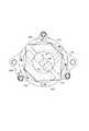
図8は電子回路内蔵型モータ2の平面図であり、図9は図8の矢印K方向に見た側面図であり、図10は斜視図である。なお、図中では、カバー及びプリント基板を省略した。  8 is a plan view of themotor 2 with built-in electronic circuit, FIG. 9 is a side view seen in the direction of arrow K in FIG. 8, and FIG. 10 is a perspective view. In the drawing, the cover and the printed circuit board are omitted.

図8に示すように、電子回路内蔵型モータ2は、6つの半導体モジュール501、502、503、504、505、506を備えている。これら半導体モジュール501〜506を区別する場合、図8中の記号を用い、U1半導体モジュール501、V1半導体モジュール502、W1半導体モジュール503、U2半導体モジュール504、V2半導体モジュール505、W2半導体モジュール506と記述することとする。  As shown in FIG. 8, the electronic circuit built-inmotor 2 includes sixsemiconductor modules 501, 502, 503, 504, 505, and 506. When thesemiconductor modules 501 to 506 are distinguished, the symbols in FIG. 8 are used to describe theU1 semiconductor module 501, theV1 semiconductor module 502, theW1 semiconductor module 503, theU2 semiconductor module 504, theV2 semiconductor module 505, and theW2 semiconductor module 506. I decided to.

ここで、U1〜W1の3つの半導体モジュール501〜503、及び、U2〜W2の3つの半導体モジュール504〜506は、バスバー507で連結されてモジュールユニットを形成している。バスバー507が連結機能を有すると共に電源ラインを兼ねることは、上記形態と同様である。  Here, the threesemiconductor modules 501 to 503 U1 to W1 and the threesemiconductor modules 504 to 506 U2 to W2 are connected by abus bar 507 to form a module unit. Thebus bar 507 has a connecting function and also serves as a power supply line as in the above embodiment.

次に、半導体モジュール501〜506の配置について説明する。
半導体モジュール501〜506は、モータケース101の端部106からシャフト401の中心線方向と同方向へ延設されたヒートシンク611に対し取り付けられている。
Next, the arrangement of thesemiconductor modules 501 to 506 will be described.
Thesemiconductor modules 501 to 506 are attached to aheat sink 611 extending from theend portion 106 of themotor case 101 in the same direction as the center line direction of theshaft 401.

そこでヒートシンク611について説明しておく。
ヒートシンク611は、図8に示すように、軸方向に垂直な断面における形状が円筒形状であり、内部には、角柱形状の空間が形成されている。言い換えれば、ヒートシンク611は、シャフト401の中心線の周りに側壁612を有している。この場合、ヒートシンク611の外壁面が、電子回路内蔵型モータ2の外郭の一部を形成している(図9、図10参照)。すなわち、ステータ201が収容された部位のモータケース103の外径とヒートシンク611の外径とが同一になっている。
Therefore, theheat sink 611 will be described.
As shown in FIG. 8, theheat sink 611 has a cylindrical shape in a cross section perpendicular to the axial direction, and a prismatic space is formed inside. In other words, theheat sink 611 has aside wall 612 around the center line of theshaft 401. In this case, the outer wall surface of theheat sink 611 forms a part of the outline of the electronic circuit built-in motor 2 (see FIGS. 9 and 10). That is, the outer diameter of themotor case 103 in the portion in which thestator 201 is accommodated is the same as the outer diameter of theheat sink 611.

また、ヒートシンク611の側壁612は、径内方向へ向く側壁面615を有している。側壁面615は、円周方向に計6つ形成されている。  Further, theside wall 612 of theheat sink 611 has aside wall surface 615 that faces inward in the radial direction. A total of six side wall surfaces 615 are formed in the circumferential direction.

以上のように形成されたヒートシンク611に対し、半導体モジュール501〜506は、径内方向を向く側壁面615に一つずつ配置されている。ここで、半導体モジュール501〜506は、その放熱面が側壁面615に接触するように配置されている。このとき、側壁面615は平面で構成されており、これに合わせて、半導体モジュール501〜506の放熱面も平面となっている。  With respect to theheat sink 611 formed as described above, thesemiconductor modules 501 to 506 are arranged one by one on theside wall surface 615 facing the radially inward direction. Here, thesemiconductor modules 501 to 506 are arranged such that their heat dissipation surfaces are in contact with the side wall surfaces 615. At this time, theside wall surface 615 is a flat surface, and the heat radiation surfaces of thesemiconductor modules 501 to 506 are also flat according to this.

半導体モジュール501〜506は、上述のごとくヒートシンク611の側壁面615に配置されることで、ちょうど半導体チップ面の垂線がシャフト401の中心線に垂直となっている(図10参照)。  Thesemiconductor modules 501 to 506 are arranged on theside wall surface 615 of theheat sink 611 as described above, so that the perpendicular of the semiconductor chip surface is just perpendicular to the center line of the shaft 401 (see FIG. 10).

半導体モジュール501〜506は、モータケース101側の端部に、巻線用端子(不図示)を有している。また、半導体モジュール501〜506は、反モータケース101側の端部に、6本の制御用端子509と、2本のコンデンサ用端子510とを有している(図9、図10参照)。これらの点については、上記形態と同様である。  Thesemiconductor modules 501 to 506 have winding terminals (not shown) at the end on themotor case 101 side. In addition, thesemiconductor modules 501 to 506 have sixcontrol terminals 509 and twocapacitor terminals 510 at the end on the side opposite to the motor case 101 (see FIGS. 9 and 10). About these points, it is the same as that of the said form.

図8等に示すように、半導体モジュール501〜506に対し、ヒートシンク611の反対側に、6つのコンデンサ701、702、703、704、705、706が配置されている。  As shown in FIG. 8 and the like, sixcapacitors 701, 702, 703, 704, 705, and 706 are arranged on the opposite side of theheat sink 611 with respect to thesemiconductor modules 501 to 506.

コンデンサ701〜706は、半導体モジュール501〜506に対して一つずつ、半導体モジュール501〜506の近傍に配置されている。コンデンサ701〜706は円柱形状を呈し、その軸がシャフト401の中心線に平行となるように配置されている。また、半導体モジュール501〜506の有するコンデンサ用端子510が径内方向へ折り曲げられていることで、この折り曲げられたコンデンサ用端子510に対し、コンデンサ701〜706の端子が、直接的に接続されている。  Thecapacitors 701 to 706 are arranged near thesemiconductor modules 501 to 506 one by one with respect to thesemiconductor modules 501 to 506.Capacitors 701 to 706 have a cylindrical shape and are arranged so that their axes are parallel to the center line ofshaft 401. In addition, since thecapacitor terminals 510 included in thesemiconductor modules 501 to 506 are bent inwardly, the terminals of thecapacitors 701 to 706 are directly connected to thebent capacitor terminals 510. Yes.

また、シャフト401が貫通した状態で、チョークコイル52が配置されている(図10参照)。チョークコイル52はドーナツ状の鉄心にコイル線が巻回されてなる。  Further, thechoke coil 52 is disposed with theshaft 401 penetrating (see FIG. 10). Thechoke coil 52 is formed by winding a coil wire around a donut-shaped iron core.

このように、径方向外側から径方向内側へ向かって、ヒートシンク611及び、半導体モジュール501〜506、コンデンサ701〜706、チョークコイル52が順に配置されている。これにより、径方向の空間が有効に活用されている。  Thus, theheat sink 611, thesemiconductor modules 501 to 506, thecapacitors 701 to 706, and thechoke coil 52 are arranged in this order from the radially outer side to the radially inner side. Thereby, the radial space is effectively utilized.

次に、本形態の電子回路内蔵型モータ2が発揮する効果について説明する。
本形態の電子回路内蔵型モータ2によっても、上記形態で説明した効果(1)〜(4)、(6)〜(8)、(10)〜(14)と同様の効果が奏される。
Next, the effect which the electronic circuit built-intype motor 2 of this form exhibits is demonstrated.
Also with the electronic circuit built-intype motor 2 of this embodiment, the same effects as the effects (1) to (4), (6) to (8), and (10) to (14) described in the above embodiment are produced.

特に本形態の電子回路内蔵型モータ2では、半導体モジュール501〜506に対しヒートシンク611の反対側にコンデンサ701〜706が配置されている。これにより、コンデンサ701〜706用のスペースをヒートシンク611に形成する必要がない。  In particular, in the electronic circuit built-inmotor 2 of this embodiment,capacitors 701 to 706 are arranged on the opposite side of theheat sink 611 with respect to thesemiconductor modules 501 to 506. Thereby, it is not necessary to form a space for thecapacitors 701 to 706 in theheat sink 611.

なお、本形態では特に、半導体モジュール501〜506が「半導体モジュール」を構成し、コンデンサ701〜706が「コンデンサ」を構成し、ヒートシンク611が「ヒートシンク」を構成し、側壁612が「側壁」を構成し、側壁面615が「側壁面」を構成する。  In this embodiment, in particular, thesemiconductor modules 501 to 506 constitute a “semiconductor module”, thecapacitors 701 to 706 constitute a “capacitor”, theheat sink 611 constitutes a “heat sink”, and theside wall 612 constitutes the “side wall”. Theside wall surface 615 forms a “side wall surface”.

(第3実施形態)
次に、第3実施形態の電子回路内蔵型モータ3について説明する。なお、上記形態と同様、パワー部50の構成を中心に説明する。また、煩雑になることを避けるため、流用できる符号は、上記形態のものを流用する。
(Third embodiment)
Next, the electronic circuit built-inmotor 3 of the third embodiment will be described. In addition, it demonstrates centering around the structure of thepower part 50 similarly to the said form. Moreover, in order to avoid complication, the code | symbol which can be diverted uses the thing of the said form.

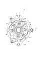
図11は電子回路内蔵型モータ3の平面図であり、図12は図11の矢印K方向に見た側面図であり、図13は斜視図である。なお、図中では、カバー及びプリント基板を省略した。  11 is a plan view of themotor 3 with built-in electronic circuit, FIG. 12 is a side view seen in the direction of arrow K in FIG. 11, and FIG. 13 is a perspective view. In the drawing, the cover and the printed circuit board are omitted.

図11に示すように、電子回路内蔵型モータ3は、6つの半導体モジュール511、512、513、514、515、516を備えている。これら半導体モジュール511〜516を区別する場合、図11中の記号を用い、U1半導体モジュール511、V1半導体モジュール512、W1半導体モジュール513、U2半導体モジュール514、V2半導体モジュール515、W2半導体モジュール516と記述することとする。  As shown in FIG. 11, the electronic circuit built-inmotor 3 includes sixsemiconductor modules 511, 512, 513, 514, 515, and 516. In order to distinguish thesesemiconductor modules 511 to 516, the symbols in FIG. 11 are used to describe theU1 semiconductor module 511, theV1 semiconductor module 512, theW1 semiconductor module 513, theU2 semiconductor module 514, theV2 semiconductor module 515, and theW2 semiconductor module 516. I decided to.

U1〜W1の3つの半導体モジュール511〜513、及び、U2〜W2の3つの半導体モジュール514〜516は、バスバー507で連結されてモジュールユニットを形成している。バスバー507が連結機能を有すると共に電源ラインを兼ねることは、上記形態と同様である。  The threesemiconductor modules 511 to 513 of U1 to W1 and the threesemiconductor modules 514 to 516 of U2 to W2 are connected by abus bar 507 to form a module unit. Thebus bar 507 has a connecting function and also serves as a power supply line as in the above embodiment.

次に、半導体モジュール511〜516の配置について説明する。
半導体モジュール511〜516は、モータケース101の端部106からシャフト401の中心線方向と同方向へ延設されたヒートシンク621に対し取り付けられている。
Next, the arrangement of thesemiconductor modules 511 to 516 will be described.
Thesemiconductor modules 511 to 516 are attached to aheat sink 621 extending from theend portion 106 of themotor case 101 in the same direction as the center line direction of theshaft 401.

そこでヒートシンク621について説明しておく。
ヒートシンク621は、図11に示すように、軸方向に垂直な断面における形状が略半円形状の2つの柱状部材がシャフト401の中心線を挟むよう並べられ、さらに、中心に円柱形状の空間が形成されるように所定半径部分を切り欠いた形状となっている。言い換えれば、ヒートシンク621は、全体として見ると、肉厚の円筒形状とも言え、シャフト401の中心線の周りに側壁622を有している。側壁622には、不連続部分を構成する2つの切り欠き部623、624が設けられている。
Therefore, theheat sink 621 will be described.
As shown in FIG. 11, in theheat sink 621, two columnar members having a substantially semicircular shape in a cross section perpendicular to the axial direction are arranged so as to sandwich the center line of theshaft 401, and a cylindrical space is formed at the center. A predetermined radius portion is cut out so as to be formed. In other words, theheat sink 621 can be said to be a thick cylindrical shape as a whole, and has aside wall 622 around the center line of theshaft 401. Theside wall 622 is provided with twonotches 623 and 624 constituting a discontinuous portion.

また、ヒートシンク621の側壁622は、径外方向へ向く側壁面625を有している。側壁面625は、円柱外周面である。側壁面625の径内方向には、中心の円柱形状の空間に開口する収容部626が形成されている。  Further, theside wall 622 of theheat sink 621 has aside wall surface 625 that faces in a radially outward direction. Theside wall surface 625 is a cylindrical outer peripheral surface. In the radially inward direction of theside wall surface 625, ahousing portion 626 that opens to a central cylindrical space is formed.

以上のように形成されたヒートシンク621に対し、半導体モジュール511〜516は、径外方向を向く側壁面625に配置されている。ここで、半導体モジュール511〜516は、その放熱面が側壁面625に接触するように配置されている。このとき、側壁面625は円柱外周面であり、凸曲面で構成されている。これに合わせて、半導体モジュール511〜516の放熱面は凹曲面となっている。  With respect to theheat sink 621 formed as described above, thesemiconductor modules 511 to 516 are disposed on theside wall surface 625 facing the radially outward direction. Here, thesemiconductor modules 511 to 516 are arranged such that their heat radiation surfaces are in contact with the side wall surfaces 625. At this time, theside wall surface 625 is a cylindrical outer peripheral surface, and is configured by a convex curved surface. In accordance with this, the heat radiation surfaces of thesemiconductor modules 511 to 516 are concave curved surfaces.

また、半導体モジュール511〜516は、上述のごとくヒートシンク621の側壁面625に配置されることで、ちょうど半導体チップ面の垂線がシャフト401の中心線に垂直となっている。  Further, thesemiconductor modules 511 to 516 are arranged on theside wall surface 625 of theheat sink 621 as described above, so that the perpendicular of the semiconductor chip surface is just perpendicular to the center line of theshaft 401.

さらにまた、半導体モジュール511〜516は、モータケース101側の端部に、巻線用端子508を有している。また、半導体モジュール511〜516は、反モータケース101側の端部に、6本の制御用端子509と、2本のコンデンサ用端子510とを有している(図12、図13参照)。これらの点については、上記形態と同様である。  Furthermore, thesemiconductor modules 511 to 516 have a windingterminal 508 at the end on themotor case 101 side. Moreover, thesemiconductor modules 511 to 516 have sixcontrol terminals 509 and twocapacitor terminals 510 at the end on the side opposite to the motor case 101 (see FIGS. 12 and 13). About these points, it is the same as that of the said form.

図11等に示すように、半導体モジュール511〜516に対し、ヒートシンク621と同じ側に、6つのコンデンサ701、702、703、704、705、706が配置されている。具体的には、ヒートシンク621の収容部626に配置されている。  As shown in FIG. 11 and the like, sixcapacitors 701, 702, 703, 704, 705, and 706 are arranged on the same side as theheat sink 621 with respect to thesemiconductor modules 511 to 516. Specifically, it is disposed in thehousing portion 626 of theheat sink 621.

コンデンサ701〜706は、半導体モジュール511〜516に対して一つずつ、半導体モジュール511〜516の近傍に配置されている。コンデンサ701〜706は円柱形状を呈し、その軸がシャフト401の中心線に平行となるように配置されている。また、半導体モジュール511〜516の有するコンデンサ用端子510が径内方向へ折り曲げられていることで、この折り曲げられたコンデンサ用端子510に対し、コンデンサ701〜706の端子が、直接的に接続されている。  Thecapacitors 701 to 706 are arranged near thesemiconductor modules 511 to 516 one by one with respect to thesemiconductor modules 511 to 516.Capacitors 701 to 706 have a cylindrical shape and are arranged so that their axes are parallel to the center line ofshaft 401. Further, since thecapacitor terminals 510 included in thesemiconductor modules 511 to 516 are bent inwardly, the terminals of thecapacitors 701 to 706 are directly connected to thebent capacitor terminals 510. Yes.

また、シャフト401が貫通した状態で、チョークコイル52が配置されている(図13参照)。チョークコイル52はドーナツ状の鉄心にコイル線が巻回されてなる。チョークコイル52のコイル端は、ヒートシンク621の一方の切り欠き部623から径外方向へ引き出されている(図11参照)。  Further, thechoke coil 52 is disposed with theshaft 401 penetrating (see FIG. 13). Thechoke coil 52 is formed by winding a coil wire around a donut-shaped iron core. The coil end of thechoke coil 52 is drawn out from the onenotch 623 of theheat sink 621 in the radially outward direction (see FIG. 11).

次に、本形態の電子回路内蔵型モータ3が発揮する効果について説明する。
本形態の電子回路内蔵型モータ3によっても、上記形態の効果(1)〜(6)、(8)〜(14)と同様の効果が奏される。
Next, the effect exerted by the electronic circuit built-inmotor 3 of this embodiment will be described.
Also by the electronic circuit built-intype motor 3 of this embodiment, the same effects as the effects (1) to (6) and (8) to (14) of the above embodiment are produced.

特に本形態の電子回路内蔵型モータ3では、ヒートシンク621の側壁面625が円柱外周面となっており、ヒートシンク621自体が略円筒状となっている。これにより、ヒートシンク621の形成が容易になる。  In particular, in the electronic circuit built-intype motor 3 of this embodiment, theside wall surface 625 of theheat sink 621 is a cylindrical outer peripheral surface, and theheat sink 621 itself is substantially cylindrical. Thereby, formation of theheat sink 621 becomes easy.

なお、本形態では、半導体モジュール511〜516が「半導体モジュール」を構成し、コンデンサ701〜706が「コンデンサ」を構成し、ヒートシンク621が「ヒートシンク」を構成し、側壁622が「側壁」を構成し、側壁面625が「側壁面」を構成し、切り欠き部623、624が「切り欠き部」を構成し、収容部626が「収容部」を構成する。  In this embodiment, thesemiconductor modules 511 to 516 form a “semiconductor module”, thecapacitors 701 to 706 form a “capacitor”, theheat sink 621 forms a “heat sink”, and theside wall 622 forms a “side wall”. Theside wall surface 625 constitutes a “side wall surface”, thenotches 623 and 624 constitute “notches”, and theaccommodating portion 626 constitutes “accommodating portion”.

(第4実施形態)
次に、第4実施形態の電子回路内蔵型モータ4について説明する。なお、上記形態と同様、パワー部50の構成を中心に説明する。また、煩雑になることを避けるため、流用できる符号は、上記形態のものを流用する。
(Fourth embodiment)
Next, the electronic circuit built-inmotor 4 of the fourth embodiment will be described. In addition, it demonstrates centering around the structure of thepower part 50 similarly to the said form. Moreover, in order to avoid complication, the code | symbol which can be diverted uses the thing of the said form.

図14は電子回路内蔵型モータ4の平面図であり、図15は図14の矢印K方向に見た側面図であり、図16は斜視図である。なお、図中では、カバー及びプリント基板を省略した。  14 is a plan view of themotor 4 with built-in electronic circuit, FIG. 15 is a side view seen in the direction of arrow K in FIG. 14, and FIG. 16 is a perspective view. In the drawing, the cover and the printed circuit board are omitted.

図14に示すように、電子回路内蔵型モータ4は、6つの半導体モジュール521、522、523、524、525、526を備えている。これら半導体モジュール521〜526を区別する場合、図14中の記号を用い、U1半導体モジュール521、V1半導体モジュール522、W1半導体モジュール523、U2半導体モジュール524、V2半導体モジュール525、W2半導体モジュール526と記述することとする。  As shown in FIG. 14, the electronic circuit built-inmotor 4 includes sixsemiconductor modules 521, 522, 523, 524, 525, and 526. In order to distinguish thesesemiconductor modules 521 to 526, the symbols in FIG. I decided to.

U1〜W1の3つの半導体モジュール521〜523、及び、U2〜W2の3つの半導体モジュール524〜526は、バスバー507で連結されてモジュールユニットを形成している。バスバー507が連結機能を有すると共に電源ラインを兼ねることは、上記形態と同様である。  The threesemiconductor modules 521 to 523 of U1 to W1 and the threesemiconductor modules 524 to 526 of U2 to W2 are connected by abus bar 507 to form a module unit. Thebus bar 507 has a connecting function and also serves as a power supply line as in the above embodiment.

次に、半導体モジュール521〜526の配置について説明する。
半導体モジュール521〜526は、モータケース101の端部106からシャフト401の中心線方向と同方向へ延設されたヒートシンク631に対し取り付けられている。
Next, the arrangement of thesemiconductor modules 521 to 526 will be described.
Thesemiconductor modules 521 to 526 are attached to aheat sink 631 that extends from theend portion 106 of themotor case 101 in the same direction as the center line direction of theshaft 401.

そこでヒートシンク631について説明しておく。
ヒートシンク631は、図14に示すように、軸方向に垂直な断面における形状が円筒形状であり、内部には、円柱形状の空間が形成されている。言い換えれば、ヒートシンク631は、シャフト401の中心線の周りに側壁632を有している。この場合、ヒートシンク631の外壁面が、電子回路内蔵型モータ4の外郭の一部を形成している(図15、図16参照)。
Therefore, theheat sink 631 will be described.
As shown in FIG. 14, theheat sink 631 has a cylindrical shape in a cross section perpendicular to the axial direction, and a columnar space is formed inside. In other words, theheat sink 631 has aside wall 632 around the center line of theshaft 401. In this case, the outer wall surface of theheat sink 631 forms a part of the outline of themotor 4 with a built-in electronic circuit (see FIGS. 15 and 16).

また、ヒートシンク631の側壁632は、径内方向へ向く側壁面635を有している。側壁面635は、円筒内周面である。  Further, theside wall 632 of theheat sink 631 has aside wall surface 635 facing inwardly in the radial direction. Theside wall surface 635 is a cylindrical inner peripheral surface.

以上のように形成されたヒートシンク631に対し、半導体モジュール521〜526は、径内方向を向く側壁面635に配置されている。半導体モジュール521〜526は、その放熱面が側壁面635に接触するように配置されている。このとき、側壁面635が凹曲面であるため、これに合わせて、半導体モジュール521〜526の放熱面は凸曲面となっている。  With respect to theheat sink 631 formed as described above, thesemiconductor modules 521 to 526 are arranged on theside wall surface 635 facing the radially inward direction. Thesemiconductor modules 521 to 526 are arranged such that their heat dissipation surfaces are in contact with the side wall surfaces 635. At this time, since theside wall surface 635 is a concave curved surface, the heat radiation surface of thesemiconductor modules 521 to 526 is a convex curved surface in accordance with this.

半導体モジュール521〜526は、上述のごとくヒートシンク631の側壁面635に配置されることで、ちょうど半導体チップ面の垂線がシャフト401の中心線に垂直となっている。  Thesemiconductor modules 521 to 526 are arranged on theside wall surface 635 of theheat sink 631 as described above, so that the perpendicular of the semiconductor chip surface is just perpendicular to the center line of theshaft 401.

半導体モジュール521〜526は、モータケース101側の端部に、巻線用端子(不図示)を有している。また、半導体モジュール521〜526は、反モータケース101側の端部に、6本の制御用端子509と、2本のコンデンサ用端子510とを有している(図15、図16参照)。これらの点については、上記形態と同様である。  Thesemiconductor modules 521 to 526 have winding terminals (not shown) at the end on themotor case 101 side. Moreover, thesemiconductor modules 521 to 526 have sixcontrol terminals 509 and twocapacitor terminals 510 at the end on the side opposite to the motor case 101 (see FIGS. 15 and 16). About these points, it is the same as that of the said form.

図14等に示すように、半導体モジュール521〜526に対し、ヒートシンク631の反対側に、6つのコンデンサ701、702、703、704、705、706が配置されている。  As shown in FIG. 14 and the like, sixcapacitors 701, 702, 703, 704, 705, and 706 are arranged on the opposite side of theheat sink 631 with respect to thesemiconductor modules 521 to 526.

コンデンサ701〜706は、半導体モジュール521〜526に対して一つずつ、半導体モジュール521〜526の近傍に配置されている。コンデンサ701〜706は円柱形状を呈し、その軸がシャフト401の中心線に平行となるように配置されている。また、半導体モジュール521〜526の有するコンデンサ用端子510が径内方向へ折り曲げられていることで、この折り曲げられたコンデンサ用端子510に対し、コンデンサ701〜706の端子が、直接的に接続されている。  Thecapacitors 701 to 706 are arranged near thesemiconductor modules 521 to 526 one by one with respect to thesemiconductor modules 521 to 526.Capacitors 701 to 706 have a cylindrical shape and are arranged so that their axes are parallel to the center line ofshaft 401. Further, since thecapacitor terminals 510 included in thesemiconductor modules 521 to 526 are bent inwardly, the terminals of thecapacitors 701 to 706 are directly connected to thebent capacitor terminals 510. Yes.

また、シャフト401が貫通した状態で、チョークコイル52が配置されている(図16参照)。チョークコイル52はドーナツ状の鉄心にコイル線が巻回されてなる。  Further, thechoke coil 52 is disposed with theshaft 401 penetrating (see FIG. 16). Thechoke coil 52 is formed by winding a coil wire around a donut-shaped iron core.

本形態の電子回路内蔵型モータ4によっても、上記形態の効果(1)〜(4)、(6)、(8)、(10)〜(14)と同様の効果が奏される。  Also by the electronic circuit built-intype motor 4 of this embodiment, the same effects as the effects (1) to (4), (6), (8), and (10) to (14) of the above embodiment are produced.

特に本形態の電子回路内蔵型モータ4では、半導体モジュール521〜526に対しヒートシンク631の反対側にコンデンサ701〜706が配置されている。これにより、コンデンサ701〜706用のスペースをヒートシンク631に形成する必要がない。
また、電子回路内蔵型モータ4では、ヒートシンク631の側壁面635が円筒内周面となっており、ヒートシンク631自体が円筒状となっている。これにより、ヒートシンク631の形成が容易になる。
In particular, in the electronic circuit built-inmotor 4 of this embodiment,capacitors 701 to 706 are arranged on the opposite side of theheat sink 631 with respect to thesemiconductor modules 521 to 526. Thereby, it is not necessary to form a space for thecapacitors 701 to 706 in theheat sink 631.
In themotor 4 with built-in electronic circuit, theside wall surface 635 of theheat sink 631 is a cylindrical inner peripheral surface, and theheat sink 631 itself is cylindrical. Thereby, formation of theheat sink 631 becomes easy.

なお、本形態では特に、半導体モジュール521〜526が「半導体モジュール」を構成し、コンデンサ701〜706が「コンデンサ」を構成し、ヒートシンク631が「ヒートシンク」を構成し、側壁632が「側壁」を構成し、側壁面635が「側壁面」を構成する。  In this embodiment, in particular, thesemiconductor modules 521 to 526 constitute a “semiconductor module”, thecapacitors 701 to 706 constitute a “capacitor”, theheat sink 631 constitutes a “heat sink”, and theside wall 632 constitutes a “side wall”. Theside wall surface 635 constitutes a “side wall surface”.

(第5実施形態)
次に、第5実施形態の電子回路内蔵型モータ5について説明する。なお、上記形態と同様、パワー部50の構成を中心として説明する。また、煩雑になることを避けるため、流用できる符号は、上記形態のものを流用する。
(Fifth embodiment)
Next, an electronic circuit built-inmotor 5 according to a fifth embodiment will be described. In addition, it demonstrates centering around the structure of thepower part 50 similarly to the said form. Moreover, in order to avoid complication, the code | symbol which can be diverted uses the thing of the said form.

図17は電子回路内蔵型モータ5の平面図であり、図18は図17の矢印K方向に見た側面図であり、図19は斜視図である。なお、図中では、カバー及びプリント基板を省略した。  17 is a plan view of themotor 5 with built-in electronic circuit, FIG. 18 is a side view seen in the direction of arrow K in FIG. 17, and FIG. 19 is a perspective view. In the drawing, the cover and the printed circuit board are omitted.

図17に示すように、電子回路内蔵型モータ5は、6つの半導体モジュール531、532、533、534、535、536を備えている。
半導体モジュール531〜536は、モータケース101の端部106からシャフト401の中心線方向と同方向へ延設されたヒートシンク641に対し取り付けられている。
As shown in FIG. 17, the motor with built-inelectronic circuit 5 includes sixsemiconductor modules 531, 532, 533, 534, 535, and 536.
Thesemiconductor modules 531 to 536 are attached to aheat sink 641 that extends from theend portion 106 of themotor case 101 in the same direction as the center line direction of theshaft 401.

そこでヒートシンク641について説明しておく。
ヒートシンク641は、図17に示すように、軸方向に垂直な断面における形状が略台形状の2つの柱状部材がシャフト401の中心線を挟むよう並べられ、さらに、中心に円柱形状の空間が形成されるように所定半径部分を切り欠いた形状となっている。このとき、上記形態のヒートシンク601(図2参照)との違いは、径方向外側の壁面がモータケース101から離れるに従ってシャフト401の中心線へ近づくように傾斜していることである。言い換えれば、ヒートシンク641は、全体として見ると、底面がモータケース101側に位置する角錐台のような形状である。ヒートシンク641は、シャフト401の中心線の周りに側壁642を有している。側壁642には、不連続部分を構成する2つの切り欠き部643、644が設けられている。
Therefore, theheat sink 641 will be described.
As shown in FIG. 17, theheat sink 641 is arranged such that two columnar members having a substantially trapezoidal shape in a cross section perpendicular to the axial direction sandwich the center line of theshaft 401, and further, a cylindrical space is formed at the center. As shown, the predetermined radius portion is cut out. At this time, the difference from theheat sink 601 of the above configuration (see FIG. 2) is that the radially outer wall surface is inclined so as to approach the center line of theshaft 401 as the distance from themotor case 101 increases. In other words, when viewed as a whole, theheat sink 641 has a shape like a truncated pyramid whose bottom surface is located on themotor case 101 side. Theheat sink 641 has aside wall 642 around the center line of theshaft 401. Theside wall 642 is provided with twonotches 643 and 644 that form discontinuous portions.

また、ヒートシンク641の側壁642は、径外方向へ向く6つの側壁面645を有している。側壁面645は、平面であって傾斜している。各側壁面645の径内方向には、中心の円柱形状の空間に開口する収容部646が形成されている。  Further, theside wall 642 of theheat sink 641 has six side wall surfaces 645 facing outward in the radial direction. Theside wall surface 645 is a flat surface and is inclined. In the radially inward direction of eachside wall surface 645, anaccommodating portion 646 that opens to a central cylindrical space is formed.

以上のように形成されたヒートシンク641に対し、半導体モジュール531〜536は、径外方向を向く側壁面645に配置されている。半導体モジュール531〜536は、その放熱面が側壁面645に接触するように配置されている。このとき、側壁面645は平面であり、これに合わせて、半導体モジュール531〜536の放熱面も平面となっている。  With respect to theheat sink 641 formed as described above, thesemiconductor modules 531 to 536 are arranged on theside wall surface 645 facing the radially outward direction. Thesemiconductor modules 531 to 536 are arranged such that their heat dissipation surfaces are in contact with the side wall surfaces 645. At this time, theside wall surface 645 is a flat surface, and the heat radiation surfaces of thesemiconductor modules 531 to 536 are also flat according to this.

また、半導体モジュール531〜536は、上述のごとくヒートシンク641の側壁面645に配置されることで、シャフト401の中心線に対し傾斜して配置されている。  In addition, thesemiconductor modules 531 to 536 are disposed on theside wall surface 645 of theheat sink 641 as described above, and thus are inclined with respect to the center line of theshaft 401.

さらにまた、半導体モジュール531〜536は、モータケース101側の端部に、巻線用端子508を有している。また、半導体モジュール531〜536は、反モータケース101側の端部に、6本の制御用端子509と、2本のコンデンサ用端子510とを有している(図18、図19参照)。これらの点については、上記形態と同様である。  Furthermore, thesemiconductor modules 531 to 536 have a windingterminal 508 at the end on themotor case 101 side. Further, thesemiconductor modules 531 to 536 have sixcontrol terminals 509 and twocapacitor terminals 510 at the end on the side opposite to the motor case 101 (see FIGS. 18 and 19). About these points, it is the same as that of the said form.

図17等に示すように、半導体モジュール531〜536に対し、ヒートシンク641と同じ側に、6つのコンデンサ701、702、703、704、705、706が配置されている。具体的には、ヒートシンク641の収容部646に配置されている。  As shown in FIG. 17 and the like, sixcapacitors 701, 702, 703, 704, 705, and 706 are arranged on the same side as theheat sink 641 with respect to thesemiconductor modules 531 to 536. Specifically, it is disposed in theaccommodating portion 646 of theheat sink 641.

コンデンサ701〜706は、半導体モジュール531〜536に対して一つずつ、半導体モジュール531〜536の近傍に配置されている。コンデンサ701〜706は円柱形状を呈し、その軸がシャフト401の中心線に平行となるように配置されている。また、半導体モジュール531〜536の有するコンデンサ用端子510が径内方向へ折り曲げられていることで、この折り曲げられたコンデンサ用端子510に対し、コンデンサ701〜706の端子が、直接的に接続されている(図19参照)。  Thecapacitors 701 to 706 are arranged in the vicinity of thesemiconductor modules 531 to 536 one by one with respect to thesemiconductor modules 531 to 536.Capacitors 701 to 706 have a cylindrical shape and are arranged so that their axes are parallel to the center line ofshaft 401. Further, since thecapacitor terminals 510 included in thesemiconductor modules 531 to 536 are bent inwardly, the terminals of thecapacitors 701 to 706 are directly connected to thebent capacitor terminals 510. (See FIG. 19).

また、シャフト401が貫通した状態で、チョークコイル52が配置されている(図19参照)。チョークコイル52はドーナツ状の鉄心にコイル線が巻回されてなる。チョークコイル52のコイル端は、ヒートシンク641の一方の切り欠き部643から径外方向へ引き出されている(図17参照)。  Thechoke coil 52 is disposed with theshaft 401 penetrating (see FIG. 19). Thechoke coil 52 is formed by winding a coil wire around a donut-shaped iron core. The coil end of thechoke coil 52 is led out radially outward from onenotch 643 of the heat sink 641 (see FIG. 17).

次に、本形態の電子回路内蔵型モータ5が発揮する効果について説明する。
本形態の電子回路内蔵型モータ5によっても、上記形態で説明した効果(1)、(3)〜(13)と同様の効果が奏される。
Next, the effect which the electronic circuit built-intype motor 5 of this form exhibits is demonstrated.
The electronic circuit built-intype motor 5 of this embodiment also has the same effects as the effects (1) and (3) to (13) described in the above embodiment.

特に本形態の電子回路内蔵型モータ5では、半導体モジュール531〜536が傾斜して配置されているため、軸方向の体格を一層小さくすることができる。
また、モータケース101の端部106から離間するに連れてシャフト401の中心線に近づくように側壁面645が傾斜しているため、ヒートシンク641を鋳造加工により形成する場合、当該加工が比較的容易になる。
In particular, in the electronic circuit built-intype motor 5 of this embodiment, thesemiconductor modules 531 to 536 are arranged to be inclined, so that the physique in the axial direction can be further reduced.
Further, since theside wall surface 645 is inclined so as to approach the center line of theshaft 401 as it is separated from theend portion 106 of themotor case 101, when theheat sink 641 is formed by casting, the processing is relatively easy. become.

なお、本形態では、半導体モジュール531〜536が「半導体モジュール」を構成し、コンデンサ701〜706が「コンデンサ」を構成し、ヒートシンク641が「ヒートシンク」を構成し、側壁642が「側壁」を構成し、側壁面645が「側壁面」を構成し、切り欠き部643、644が「切り欠き部」を構成し、収容部646が「収容部」を構成する。  In this embodiment, thesemiconductor modules 531 to 536 constitute a “semiconductor module”, thecapacitors 701 to 706 constitute a “capacitor”, theheat sink 641 constitutes a “heat sink”, and theside wall 642 constitutes a “side wall”. Theside wall surface 645 forms a “side wall surface”, thecutout portions 643 and 644 form a “cutout portion”, and thehousing portion 646 forms a “housing portion”.

(第6実施形態)
次に、第6実施形態の電子回路内蔵型モータ6について説明する。なお、上記形態と同様、パワー部50の構成を中心として説明する。さらにまた、煩雑になることを避けるため、流用できる符号は、上記形態のものを流用する。
(Sixth embodiment)
Next, an electronic circuit built-inmotor 6 according to a sixth embodiment will be described. In addition, it demonstrates centering around the structure of thepower part 50 similarly to the said form. Furthermore, in order to avoid complication, the code | symbol which can be diverted uses the thing of the said form.

図20は電子回路内蔵型モータ6の平面図であり、図21は図20の矢印K方向に見た側面図であり、図22は斜視図である。なお、図中では、カバー及びプリント基板を省略した。  20 is a plan view of themotor 6 with built-in electronic circuit, FIG. 21 is a side view seen in the direction of arrow K in FIG. 20, and FIG. 22 is a perspective view. In the drawing, the cover and the printed circuit board are omitted.

図20に示すように、電子回路内蔵型モータ6は、6つの半導体モジュール531、532、533、534、535、536を備えている。
半導体モジュール531〜536は、モータケース101の端部106からシャフト401の中心線方向と同方向へ延設されたヒートシンク651に対し取り付けられている。
As shown in FIG. 20, the electronic circuit built-inmotor 6 includes sixsemiconductor modules 531, 532, 533, 534, 535, and 536.
Thesemiconductor modules 531 to 536 are attached to aheat sink 651 extending from theend portion 106 of themotor case 101 in the same direction as the center line direction of theshaft 401.

そこでヒートシンク651について説明しておく。
ヒートシンク651は、図20に示すように、軸方向に垂直な断面における形状が円筒形状であり、内部には、角錐台形状の空間が形成されている。ヒートシンク651は、シャフト401の中心線の周りに側壁652を有している。この場合、ヒートシンク651の外壁面が、電子回路内蔵型モータ6の外郭の一部を形成している(図21、図22参照)。
Therefore, theheat sink 651 will be described.
As shown in FIG. 20, theheat sink 651 has a cylindrical shape in a cross section perpendicular to the axial direction, and a pyramid-shaped space is formed inside. Theheat sink 651 has aside wall 652 around the center line of theshaft 401. In this case, the outer wall surface of theheat sink 651 forms a part of the outline of themotor 6 with a built-in electronic circuit (see FIGS. 21 and 22).

また、ヒートシンク651の側壁652は、径内方向へ向く側壁面655を有している。側壁面655は、円周方向に計6つ形成されている。上記形態のヒートシンク611(図8参照)と違うのは、側壁面655が傾斜していることである。具体的に、側壁面655は、モータケース101の端部106から離間するほどシャフト401の中心線から離れるように傾斜している。  Further, theside wall 652 of theheat sink 651 has aside wall surface 655 that faces inward in the radial direction. A total of six side wall surfaces 655 are formed in the circumferential direction. A difference from the heat sink 611 (see FIG. 8) of the above-described form is that theside wall surface 655 is inclined. Specifically, theside wall surface 655 is inclined so as to be away from the center line of theshaft 401 as the distance from theend portion 106 of themotor case 101 increases.

以上のように形成されたヒートシンク651に対し、半導体モジュール531〜536は、径内方向を向く側壁面655に一つずつ配置されている。半導体モジュール531〜536は、その放熱面が側壁面655に接触するように配置されている。このとき、側壁面655は平面で構成されており、これに合わせて、半導体モジュール531〜536の放熱面も平面となっている。  With respect to theheat sink 651 formed as described above, thesemiconductor modules 531 to 536 are arranged one by one on theside wall surface 655 facing the radially inward direction. Thesemiconductor modules 531 to 536 are arranged such that their heat dissipation surfaces are in contact with the side wall surfaces 655. At this time, theside wall surface 655 is constituted by a flat surface, and the heat radiation surfaces of thesemiconductor modules 531 to 536 are also flat according to this.

半導体モジュール531〜536は、上述のごとくヒートシンク651の側壁面655に配置されることで、シャフト401の中心線に対し傾斜して配置されている。  Thesemiconductor modules 531 to 536 are arranged on theside wall surface 655 of theheat sink 651 as described above, so that thesemiconductor modules 531 to 536 are arranged to be inclined with respect to the center line of theshaft 401.

また、半導体モジュール531〜536は、モータケース101側の端部に、巻線用端子508を有している(図20参照)。さらにまた、半導体モジュール531〜536は、反モータケース101側の端部に、6本の制御用端子509と、2本のコンデンサ用端子510とを有している(図21、図22参照)。これらの点については、上記形態と同様である。  Moreover, thesemiconductor modules 531 to 536 have a windingterminal 508 at the end on themotor case 101 side (see FIG. 20). Furthermore, thesemiconductor modules 531 to 536 have sixcontrol terminals 509 and twocapacitor terminals 510 at the end on the side opposite to the motor case 101 (see FIGS. 21 and 22). . About these points, it is the same as that of the said form.

図20等に示すように、半導体モジュール531〜536に対し、ヒートシンク651の反対側に、6つのコンデンサ701、702、703、704、705、706が配置されている。  As shown in FIG. 20 and the like, sixcapacitors 701, 702, 703, 704, 705, and 706 are arranged on the opposite side of theheat sink 651 with respect to thesemiconductor modules 531 to 536.

コンデンサ701〜706は、半導体モジュール531〜536に対して一つずつ、半導体モジュール531〜536の近傍に配置されている。コンデンサ701〜706は円柱形状を呈し、半導体モジュールに沿って傾斜している。また、半導体モジュール531〜536の有するコンデンサ用端子510が径内方向へ折り曲げられていることで、この折り曲げられたコンデンサ用端子510に対し、コンデンサ701〜706の端子が、直接的に接続されている。  Thecapacitors 701 to 706 are arranged in the vicinity of thesemiconductor modules 531 to 536 one by one with respect to thesemiconductor modules 531 to 536. Thecapacitors 701 to 706 have a cylindrical shape and are inclined along the semiconductor module. Further, since thecapacitor terminals 510 included in thesemiconductor modules 531 to 536 are bent inwardly, the terminals of thecapacitors 701 to 706 are directly connected to thebent capacitor terminals 510. Yes.

また、シャフト401が貫通した状態で、チョークコイル52が配置されている(図22参照)。チョークコイル52はドーナツ状の鉄心にコイル線が巻回されてなる。  Further, thechoke coil 52 is disposed with theshaft 401 penetrating (see FIG. 22). Thechoke coil 52 is formed by winding a coil wire around a donut-shaped iron core.

次に、本形態の電子回路内蔵型モータ6が発揮する効果について説明する。
本形態の電子回路内蔵型モータ6によっても、上記形態の効果(1)、(3)、(4)、(6)〜(8)、(10)〜(13)の効果が奏される。
Next, the effect exerted by the electronic circuit built-inmotor 6 of this embodiment will be described.
The effects (1), (3), (4), (6) to (8), and (10) to (13) of the above form are also exhibited by the electronic circuit built-inmotor 6 of this embodiment.

特に本形態の電子回路内蔵型モータ6では、半導体モジュール531〜536に対しヒートシンク651の反対側にコンデンサ701〜706が配置されている。これにより、コンデンサ701〜706用の収容部をヒートシンク651に形成する必要がない。  In particular, in the electronic circuit built-inmotor 6 of this embodiment,capacitors 701 to 706 are arranged on the opposite side of theheat sink 651 with respect to thesemiconductor modules 531 to 536. Thereby, it is not necessary to form the accommodating portions for thecapacitors 701 to 706 in theheat sink 651.

また、本形態の電子回路内蔵型モータ6では、半導体モジュール531〜536が傾斜して配置されているため、軸方向の体格を一層小さくすることができる。
さらにまた、モータケース101の端部106から離間するに連れてシャフト401の中心線から遠ざかるように側壁面655が傾斜しているため、ヒートシンク651を鋳造加工により形成する場合、当該加工が比較的容易になる。
Further, in the electronic circuit built-intype motor 6 of the present embodiment, thesemiconductor modules 531 to 536 are arranged to be inclined, so that the physique in the axial direction can be further reduced.
Furthermore, since theside wall surface 655 is inclined away from the center line of theshaft 401 as it is separated from theend portion 106 of themotor case 101, when theheat sink 651 is formed by casting, the processing is relatively It becomes easy.

なお、本形態では特に、半導体モジュール531〜536が「半導体モジュール」を構成し、コンデンサ701〜706が「コンデンサ」を構成し、ヒートシンク651が「ヒートシンク」を構成し、側壁652が「側壁」を構成し、側壁面655が「側壁面」を構成する。  In this embodiment, in particular, thesemiconductor modules 531 to 536 constitute a “semiconductor module”, thecapacitors 701 to 706 constitute a “capacitor”, theheat sink 651 constitutes a “heat sink”, and theside wall 652 constitutes the “side wall”. Theside wall surface 655 constitutes a “side wall surface”.

(第7実施形態)
次に、第7実施形態の電子回路内蔵型モータ7について説明する。なお、上記形態と同様、パワー部50の構成を中心として説明する。さらにまた、煩雑になることを避けるため、流用できる符号は、上記形態のものを流用する。
(Seventh embodiment)
Next, an electronic circuit built-inmotor 7 according to a seventh embodiment will be described. In addition, it demonstrates centering around the structure of thepower part 50 similarly to the said form. Furthermore, in order to avoid complication, the code | symbol which can be diverted uses the thing of the said form.

図23は電子回路内蔵型モータ7の平面図であり、図24は図23の矢印K方向に見た側面図であり、図25は斜視図である。なお、図中では、カバー及びプリント基板を省略した。  23 is a plan view of themotor 7 with built-in electronic circuit, FIG. 24 is a side view seen in the direction of arrow K in FIG. 23, and FIG. 25 is a perspective view. In the drawing, the cover and the printed circuit board are omitted.

図23に示すように、電子回路内蔵型モータ7は、6つの半導体モジュール541、542、543、544、545、546を備えている。
半導体モジュール541〜546は、モータケース101の端部106からシャフト401の中心線方向と同方向へ延設されたヒートシンク661に対し取り付けられている。
As shown in FIG. 23, the electronic circuit built-inmotor 7 includes sixsemiconductor modules 541, 542, 543, 544, 545, and 546.
Thesemiconductor modules 541 to 546 are attached to aheat sink 661 extending from theend portion 106 of themotor case 101 in the same direction as the center line direction of theshaft 401.

そこでヒートシンク661について説明しておく。
ヒートシンク661は、図23に示すように、軸方向に垂直な断面における形状が略半円形状の2つの柱状部材がシャフト401の中心線を挟むよう並べられ、さらに、中心に円柱形状の空間が形成されるように所定半径部分を切り欠いた形状となっている。このとき、上記形態のヒートシンク621(図11)との違いは、径方向外側の壁面がモータケース101から離れるに従ってシャフト401の中心線へ近づくように傾斜していることである。言い換えれば、ヒートシンク661は、全体として見ると、底面がモータケース101側に位置する円錐台のような形状である。ヒートシンク661は、シャフト401の中心線の周りに側壁662を有している。側壁662には、不連続部分を構成する2つの切り欠き部663、664が設けられている。
Therefore, theheat sink 661 will be described.
As shown in FIG. 23, theheat sink 661 is arranged so that two columnar members having a substantially semicircular shape in a cross section perpendicular to the axial direction sandwich the center line of theshaft 401, and a cylindrical space is formed at the center. A predetermined radius portion is cut out so as to be formed. At this time, the difference from the heat sink 621 (FIG. 11) of the above-mentioned form is that the radially outer wall surface is inclined so as to approach the center line of theshaft 401 as the distance from themotor case 101 increases. In other words, theheat sink 661 is shaped like a truncated cone having a bottom surface located on themotor case 101 side when viewed as a whole. Theheat sink 661 has aside wall 662 around the center line of theshaft 401. Theside wall 662 is provided with twonotches 663 and 664 that form discontinuous portions.

また、ヒートシンク661の側壁662は、径外方向へ向く側壁面665を有している。側壁面665は、円錐外周面であって傾斜している。側壁面665の径内方向には、中心の円柱形状の空間に開口する収容部666が形成されている。  Further, theside wall 662 of theheat sink 661 has aside wall surface 665 that faces in a radially outward direction. Theside wall surface 665 is a cone outer peripheral surface and is inclined. Anaccommodating portion 666 that opens into a central cylindrical space is formed in the radially inward direction of theside wall surface 665.

以上のように形成されたヒートシンク661に対し、半導体モジュール541〜546は、径外方向を向く側壁面665に配置されている。半導体モジュール541〜546は、その放熱面が側壁面665に接触するように配置されている。このとき、側壁面665は凸曲面であり、これに合わせて、半導体モジュール531〜536の放熱面は凹曲面となっている。  With respect to theheat sink 661 formed as described above, thesemiconductor modules 541 to 546 are arranged on theside wall surface 665 facing the radially outward direction. Thesemiconductor modules 541 to 546 are arranged so that their heat radiation surfaces are in contact with the side wall surfaces 665. At this time, theside wall surface 665 is a convex curved surface, and according to this, the heat radiation surfaces of thesemiconductor modules 531 to 536 are concave curved surfaces.

また、半導体モジュール541〜546は、上述のごとくヒートシンク661の側壁面665に配置されることで、シャフト401の中心線に対し傾斜している。  In addition, thesemiconductor modules 541 to 546 are disposed on theside wall surface 665 of theheat sink 661 as described above, and thus are inclined with respect to the center line of theshaft 401.

さらにまた、半導体モジュール541〜546は、モータケース101側の端部に、巻線用端子508を有している。また、半導体モジュール541〜546は、反モータケース101側の端部に、6本の制御用端子509と、2本のコンデンサ用端子510とを有している(図24、図25参照)。これらの点については、上記形態と同様である。  Furthermore, thesemiconductor modules 541 to 546 have a windingterminal 508 at the end on themotor case 101 side. Further, thesemiconductor modules 541 to 546 have sixcontrol terminals 509 and twocapacitor terminals 510 at the end on the side opposite to the motor case 101 (see FIGS. 24 and 25). About these points, it is the same as that of the said form.

図23等に示すように、半導体モジュール541〜546に対し、ヒートシンク661と同じ側に、6つのコンデンサ701、702、703、704、705、706が配置されている。具体的には、ヒートシンク661の収容部666に配置されている。  As shown in FIG. 23 and the like, sixcapacitors 701, 702, 703, 704, 705, and 706 are arranged on the same side as theheat sink 661 with respect to thesemiconductor modules 541 to 546. Specifically, it is disposed in theaccommodating portion 666 of theheat sink 661.

コンデンサ701〜706は、半導体モジュール541〜546に対して一つずつ、半導体モジュール541〜546の近傍に配置されている。コンデンサ701〜706は円柱形状を呈し、その軸がシャフト401の中心線に平行となるように配置されている。また、半導体モジュール541〜546の有するコンデンサ用端子510が径内方向へ折り曲げられていることで、この折り曲げられたコンデンサ用端子510に対し、コンデンサ701〜706の端子が、直接的に接続されている(図25参照)。  Thecapacitors 701 to 706 are arranged near thesemiconductor modules 541 to 546 one by one with respect to thesemiconductor modules 541 to 546.Capacitors 701 to 706 have a cylindrical shape and are arranged so that their axes are parallel to the center line ofshaft 401. Further, since thecapacitor terminals 510 included in thesemiconductor modules 541 to 546 are bent inwardly, the terminals of thecapacitors 701 to 706 are directly connected to thebent capacitor terminals 510. (See FIG. 25).

また、シャフト401が貫通した状態で、チョークコイル52が配置されている(図25参照)。チョークコイル52はドーナツ状の鉄心にコイル線が巻回されてなる。チョークコイル52のコイル端は、ヒートシンク661の一方の切り欠き部663から径外方向へ引き出されている(図23参照)。  Thechoke coil 52 is disposed with theshaft 401 penetrating (see FIG. 25). Thechoke coil 52 is formed by winding a coil wire around a donut-shaped iron core. The coil end of thechoke coil 52 is drawn out from the onenotch 663 of theheat sink 661 in the radially outward direction (see FIG. 23).

次に、本形態の電子回路内蔵型モータ7が発揮する効果について説明する。
本形態の電子回路内蔵型モータ7によっても、上記形態で説明した効果(1)、(3)〜(6)、(8)〜(13)と同様の効果が奏される。
Next, the effect which themotor 7 with a built-in electronic circuit of this form exhibits is demonstrated.
The electronic circuit built-intype motor 7 of this embodiment also has the same effects as the effects (1), (3) to (6), and (8) to (13) described in the above embodiment.

特に本形態の電子回路内蔵型モータ7では、半導体モジュール541〜546が傾斜して配置されているため、軸方向の体格を一層小さくすることができる。
また、ヒートシンク661が全体として見ると円錐台形状であり、また、モータケース101の端部106から離間するに連れてシャフト401の中心線に近づくように側壁面665が傾斜しているため、ヒートシンク661を鋳造加工により形成する場合、当該加工が比較的容易になる。
In particular, in the electronic circuit built-inmotor 7 according to the present embodiment, thesemiconductor modules 541 to 546 are arranged to be inclined, so that the physique in the axial direction can be further reduced.
Further, since theheat sink 661 has a truncated cone shape as a whole, and theside wall surface 665 is inclined so as to approach the center line of theshaft 401 as it is separated from theend portion 106 of themotor case 101, the heat sink When 661 is formed by casting, the processing is relatively easy.

なお、本形態では、半導体モジュール541〜546が「半導体モジュール」を構成し、コンデンサ701〜706が「コンデンサ」を構成し、ヒートシンク661が「ヒートシンク」を構成し、側壁662が「側壁」を構成し、側壁面665が「側壁面」を構成し、切り欠き部663、664が「切り欠き部」を構成し、収容部666が「収容部」を構成する。  In this embodiment, thesemiconductor modules 541 to 546 constitute a “semiconductor module”, thecapacitors 701 to 706 constitute a “capacitor”, theheat sink 661 constitute a “heat sink”, and theside wall 662 constitute a “side wall”. Theside wall surface 665 constitutes the “side wall surface”, thenotches 663 and 664 constitute the “notch”, and theaccommodating portion 666 constitutes the “accommodating portion”.

(第8実施形態)
次に、第8実施形態の電子回路内蔵型モータ8について説明する。なお、上記形態と同様、パワー部50の構成を中心として説明する。さらにまた、煩雑になることを避けるため、流用できる符号は、上記形態のものを流用する。
(Eighth embodiment)
Next, an electronic circuit built-inmotor 8 according to an eighth embodiment will be described. In addition, it demonstrates centering around the structure of thepower part 50 similarly to the said form. Furthermore, in order to avoid complication, the code | symbol which can be diverted uses the thing of the said form.

図26は電子回路内蔵型モータ8の平面図であり、図27は図26の矢印K方向に見た側面図であり、図28は斜視図である。なお、図中では、カバー及びプリント基板を省略した。  26 is a plan view of themotor 8 with built-in electronic circuit, FIG. 27 is a side view seen in the direction of arrow K in FIG. 26, and FIG. 28 is a perspective view. In the drawing, the cover and the printed circuit board are omitted.

図26に示すように、電子回路内蔵型モータ8は、6つの半導体モジュール531、532、533、534、535、536を備えている。
半導体モジュール531〜536は、モータケース101の端部106からシャフト401の中心線方向と同方向へ延設されたヒートシンク671に対し取り付けられている。
As shown in FIG. 26, the electronic circuit built-inmotor 8 includes sixsemiconductor modules 531, 532, 533, 534, 535, and 536.
Thesemiconductor modules 531 to 536 are attached to aheat sink 671 extending from theend portion 106 of themotor case 101 in the same direction as the center line direction of theshaft 401.

そこでヒートシンク671について説明しておく。
ヒートシンク671は、図26に示すように、軸方向に垂直な断面における形状が略台形状の2つの柱状部材がシャフト401の中心線を挟むよう並べられ、さらに、中心に円柱形状の空間が形成されるように所定半径部分を切り欠いた形状となっている。このとき、上記形態のヒートシンク601(図2参照)との違いは、径方向外側の壁面がモータケース101から離れるに従ってシャフト401の中心線から遠ざかるように傾斜していることである。言い換えれば、ヒートシンク671は、全体として見ると、底面に平行な面である頂面がモータケース101側に位置する角錐台のような形状となっている。ヒートシンク671は、シャフト401の中心線の周りに側壁672を有している。側壁672には、不連続部分を構成する2つの切り欠き部673、674が設けられている。
Therefore, theheat sink 671 will be described.
As shown in FIG. 26, theheat sink 671 is arranged such that two columnar members having a substantially trapezoidal shape in a cross section perpendicular to the axial direction sandwich the center line of theshaft 401, and further, a cylindrical space is formed at the center. As shown, the predetermined radius portion is cut out. At this time, the difference from theheat sink 601 of the above embodiment (see FIG. 2) is that the radially outer wall surface is inclined so as to move away from the center line of theshaft 401 as the distance from themotor case 101 increases. In other words, when viewed as a whole, theheat sink 671 has a shape like a truncated pyramid whose top surface, which is a surface parallel to the bottom surface, is located on themotor case 101 side. Theheat sink 671 has aside wall 672 around the center line of theshaft 401. Theside wall 672 is provided with twonotches 673 and 674 that constitute a discontinuous portion.

また、ヒートシンク671の側壁672は、径外方向へ向く6つの側壁面675を有している。側壁面675は、傾斜している。  Further, theside wall 672 of theheat sink 671 has six side wall surfaces 675 facing outward in the radial direction.Side wall surface 675 is inclined.

以上のように形成されたヒートシンク671に対し、半導体モジュール531〜536は、径外方向を向く側壁面675に配置されている。半導体モジュール531〜536は、その放熱面が側壁面675に接触するように配置されている。このとき、側壁面675は平面であり、これに合わせて、半導体モジュール531〜536の放熱面も平面となっている。  With respect to theheat sink 671 formed as described above, thesemiconductor modules 531 to 536 are arranged on theside wall surface 675 facing in the radially outward direction. Thesemiconductor modules 531 to 536 are arranged such that their heat dissipation surfaces are in contact with the side wall surfaces 675. At this time, theside wall surface 675 is a flat surface, and the heat radiation surfaces of thesemiconductor modules 531 to 536 are also flat according to this.

また、半導体モジュール531〜536は、上述のごとくヒートシンク671の側壁面675に配置されることで、シャフト401の中心線に対し傾斜して配置されている。  In addition, thesemiconductor modules 531 to 536 are disposed on theside wall surface 675 of theheat sink 671 as described above, and thus are inclined with respect to the center line of theshaft 401.

さらにまた、半導体モジュール531〜536は、モータケース101側の端部に、巻線用端子508を有している(図27、図28参照)。また、半導体モジュール531〜536は、反モータケース101側の端部に、6本の制御用端子509と、2本のコンデンサ用端子510とを有している(図27、図28参照)。これらの点については、上記形態と同様である。  Furthermore, thesemiconductor modules 531 to 536 have a windingterminal 508 at the end on themotor case 101 side (see FIGS. 27 and 28). Further, thesemiconductor modules 531 to 536 have sixcontrol terminals 509 and twocapacitor terminals 510 at the end on the side opposite to the motor case 101 (see FIGS. 27 and 28). About these points, it is the same as that of the said form.

図26等に示すように、半導体モジュール531〜536に対し、ヒートシンク671の反対側に、6つのコンデンサ701、702、703、704、705、706が配置されている。  As shown in FIG. 26 and the like, sixcapacitors 701, 702, 703, 704, 705, and 706 are arranged on the opposite side of theheat sink 671 with respect to thesemiconductor modules 531 to 536.

コンデンサ701〜706は、半導体モジュール531〜536に対して一つずつ、半導体モジュール531〜536の近傍に配置されている。コンデンサ701〜706は円柱形状を呈し、半導体モジュール531〜536に沿って傾斜している。また、半導体モジュール531〜536の有するコンデンサ用端子510が径外方向へ折り曲げられていることで、この折り曲げられたコンデンサ用端子510に対し、コンデンサ701〜706の端子が、直接的に接続されている(図28参照)。  Thecapacitors 701 to 706 are arranged in the vicinity of thesemiconductor modules 531 to 536 one by one with respect to thesemiconductor modules 531 to 536. Thecapacitors 701 to 706 have a cylindrical shape and are inclined along thesemiconductor modules 531 to 536. In addition, since thecapacitor terminals 510 included in thesemiconductor modules 531 to 536 are bent in the radially outward direction, the terminals of thecapacitors 701 to 706 are directly connected to thebent capacitor terminals 510. (See FIG. 28).

また、シャフト401が貫通した状態で、チョークコイル52が配置されている(図28参照)。チョークコイル52はドーナツ状の鉄心にコイル線が巻回されてなる。チョークコイル52のコイル端は、ヒートシンク671の一方の切り欠き部673から径外方向へ引き出されている。  Further, thechoke coil 52 is disposed with theshaft 401 penetrating (see FIG. 28). Thechoke coil 52 is formed by winding a coil wire around a donut-shaped iron core. The coil end of thechoke coil 52 is drawn out from onenotch portion 673 of theheat sink 671 in the radially outward direction.

次に、本形態の電子回路内蔵型モータ8が発揮する効果について説明する。
本形態の電子回路内蔵型モータ8によっても、上記形態で説明した効果(1)、(3)、(4)、(6)〜(13)と同様の効果が奏される。
Next, the effect exerted by the electronic circuit built-inmotor 8 of this embodiment will be described.
The electronic circuit built-intype motor 8 of this embodiment also has the same effects as the effects (1), (3), (4), and (6) to (13) described in the above embodiment.

特に本形態の電子回路内蔵型モータ8では、半導体モジュール531〜536が傾斜して配置されているため、軸方向の体格を一層小さくすることができる。
また、モータケース101の端部106から離間するに連れてシャフト401の中心線から遠ざかるようにヒートシンク671の側壁面675が傾斜しているため、モータケース101の端部106に、スペースを確保することができる。
さらにまた、本形態の電子回路内蔵型モータ8では、半導体モジュール531〜536に対しヒートシンク671の反対側にコンデンサ701〜706が配置されている。これにより、コンデンサ701〜706用の収容部をヒートシンク671に形成する必要がない。
In particular, in the electronic circuit built-intype motor 8 of this embodiment, thesemiconductor modules 531 to 536 are arranged to be inclined, so that the physique in the axial direction can be further reduced.
Further, since theside wall surface 675 of theheat sink 671 is inclined so as to move away from the center line of theshaft 401 as the distance from theend portion 106 of themotor case 101 increases, a space is secured in theend portion 106 of themotor case 101. be able to.
Furthermore, in the electronic circuit built-inmotor 8 of this embodiment,capacitors 701 to 706 are arranged on the opposite side of theheat sink 671 with respect to thesemiconductor modules 531 to 536. Thereby, it is not necessary to form the accommodating portions for thecapacitors 701 to 706 in theheat sink 671.

なお、本形態では、半導体モジュール531〜536が「半導体モジュール」を構成し、コンデンサ701〜706が「コンデンサ」を構成し、ヒートシンク671が「ヒートシンク」を構成し、側壁672が「側壁」を構成し、側壁面675が「側壁面」を構成し、切り欠き部673、674が「切り欠き部」を構成する。  In this embodiment, thesemiconductor modules 531 to 536 constitute a “semiconductor module”, thecapacitors 701 to 706 constitute a “capacitor”, theheat sink 671 constitutes a “heat sink”, and theside wall 672 constitutes a “side wall”. Theside wall surface 675 constitutes the “side wall surface”, and thenotches 673 and 674 constitute the “notch”.

(第9実施形態)
次に、第9実施形態の電子回路内蔵型モータ9について説明する。なお、上記形態と同様、パワー部50の構成を中心として説明する。さらにまた、煩雑になることを避けるため、流用できる符号は、上記形態のものを流用する。
(Ninth embodiment)
Next, an electronic circuit built-inmotor 9 according to a ninth embodiment will be described. In addition, it demonstrates centering around the structure of thepower part 50 similarly to the said form. Furthermore, in order to avoid complication, the code | symbol which can be diverted uses the thing of the said form.

図29は電子回路内蔵型モータ9の平面図であり、図30は図29の矢印K方向に見た側面図であり、図31は斜視図である。なお、図中では、カバーを省略し、また、図30及び図31ではモジュール部分を取り外して示している。  29 is a plan view of the electronic circuit built-inmotor 9, FIG. 30 is a side view seen in the direction of arrow K in FIG. 29, and FIG. 31 is a perspective view. In the drawing, the cover is omitted, and in FIG. 30 and FIG. 31, the module portion is removed.

図29に示すように、電子回路内蔵型モータ9は、6つの半導体モジュール501、502、503、504、505、506を備えている。これら半導体モジュール501〜506を区別する場合、図29中の記号を用い、U1半導体モジュール501、V1半導体モジュール502、W1半導体モジュール503、U2半導体モジュール504、V2半導体モジュール505、W2半導体モジュール506と記述することとする。  As shown in FIG. 29, the electronic circuit built-inmotor 9 includes sixsemiconductor modules 501, 502, 503, 504, 505, and 506. In order to distinguish thesesemiconductor modules 501 to 506, the symbols in FIG. 29 are used to describe theU1 semiconductor module 501, theV1 semiconductor module 502, theW1 semiconductor module 503, theU2 semiconductor module 504, theV2 semiconductor module 505, and theW2 semiconductor module 506. I decided to.

ここで、U1〜W1の3つの半導体モジュール501〜503、及び、U2〜W2の3つの半導体モジュール504〜506は、バスバー507で連結されてモジュールユニットを形成している。バスバー507が連結機能を有すると共に電源ラインを兼ねることは、上記形態と同様である。  Here, the threesemiconductor modules 501 to 503 U1 to W1 and the threesemiconductor modules 504 to 506 U2 to W2 are connected by abus bar 507 to form a module unit. Thebus bar 507 has a connecting function and also serves as a power supply line as in the above embodiment.

次に、半導体モジュール501〜506の配置について説明する。
上記各形態と大きく異なる部分は、電子回路内蔵型モータ9がヒートシンクを有していない点である。
半導体モジュール501〜506は、モータケース101側の端部に、巻線用端子508を有している。また、半導体モジュール501〜506は、反モータケース101側の端部に、6本の制御用端子509と、2本のコンデンサ用端子510とを有している(図30参照)。
Next, the arrangement of thesemiconductor modules 501 to 506 will be described.
A significant difference from the above embodiments is that the electronic circuit built-inmotor 9 does not have a heat sink.
Thesemiconductor modules 501 to 506 have a windingterminal 508 at the end on themotor case 101 side. Moreover, thesemiconductor modules 501 to 506 have sixcontrol terminals 509 and twocapacitor terminals 510 at the end on the side opposite to the motor case 101 (see FIG. 30).

このとき、制御用端子509は、プリント基板801のスルーホールに通され、半田付けされている。半導体モジュール501〜506は、半導体チップ面の垂線がシャフト401の中心線に垂直となるように、また、当該垂線が径方向を向くように円周上に並べられている。プリント基板801は、図30及び図31に示すように、モータケース101からシャフト401の中心線に平行に立設された2つのスペーサ681、682の先端部に螺着される。これにより、半導体モジュール501〜506がモータケース101に対して位置決めされる。  At this time, thecontrol terminal 509 is passed through the through hole of the printedboard 801 and soldered. Thesemiconductor modules 501 to 506 are arranged on the circumference so that the perpendicular of the semiconductor chip surface is perpendicular to the center line of theshaft 401 and the perpendicular is directed in the radial direction. As shown in FIGS. 30 and 31, the printedcircuit board 801 is screwed to the tip portions of twospacers 681 and 682 erected from themotor case 101 in parallel with the center line of theshaft 401. Thereby, thesemiconductor modules 501 to 506 are positioned with respect to themotor case 101.

また、図29等に示すように、半導体モジュール501〜506に対し、径方向内側に、6つのコンデンサ701、702、703、704、705、706が配置されている。  As shown in FIG. 29 and the like, sixcapacitors 701, 702, 703, 704, 705, and 706 are arranged on the radially inner side with respect to thesemiconductor modules 501 to 506.

コンデンサ701〜706は、半導体モジュール501〜506に対して一つずつ、半導体モジュール501〜506の近傍に配置されている。コンデンサ701〜706は円柱形状を呈し、その軸がシャフト401の中心線に平行となるように配置されている。また、半導体モジュール501〜506の有するコンデンサ用端子510が径内方向へ折り曲げられていることで、この折り曲げられたコンデンサ用端子510に対し、コンデンサ701〜706の端子が、直接的に接続されている。  Thecapacitors 701 to 706 are arranged near thesemiconductor modules 501 to 506 one by one with respect to thesemiconductor modules 501 to 506.Capacitors 701 to 706 have a cylindrical shape and are arranged so that their axes are parallel to the center line ofshaft 401. In addition, since thecapacitor terminals 510 included in thesemiconductor modules 501 to 506 are bent inwardly, the terminals of thecapacitors 701 to 706 are directly connected to thebent capacitor terminals 510. Yes.

次に、本形態の電子回路内蔵型モータ9が発揮する効果について説明する。
本形態の電子回路内蔵型モータ9によっても、上記形態で説明した効果(1)〜(3)、(10)〜(14)と同様の効果が奏される。
Next, the effect exerted by the electronic circuit built-inmotor 9 of this embodiment will be described.
The electronic circuit built-intype motor 9 of this embodiment also has the same effects as the effects (1) to (3) and (10) to (14) described in the above embodiments.

特に本形態は、消費電力が小さく半導体モジュール501〜506の発熱が少ない場合に有効である。  In particular, this embodiment is effective when the power consumption is small and thesemiconductor modules 501 to 506 generate little heat.

なお、本形態では、半導体モジュール501〜506が「半導体モジュール」を構成し、コンデンサ701〜706が「コンデンサ」を構成する。  In this embodiment, thesemiconductor modules 501 to 506 constitute a “semiconductor module”, and thecapacitors 701 to 706 constitute a “capacitor”.

(第10実施形態)
次に、第10実施形態の電子回路内蔵型モータ10について説明する。なお、上記形態と同様、パワー部50の構成を中心として説明する。さらにまた、煩雑になることを避けるため、流用できる符号は、上記形態のものを流用する。
(10th Embodiment)
Next, an electronic circuit built-inmotor 10 according to a tenth embodiment will be described. In addition, it demonstrates centering around the structure of thepower part 50 similarly to the said form. Furthermore, in order to avoid complication, the code | symbol which can be diverted uses the thing of the said form.

図32は電子回路内蔵型モータ10の平面図であり、図33は図32の矢印K方向に見た側面図であり、図34は斜視図である。なお、図中では、カバー及びプリント基板を省略した。  32 is a plan view of themotor 10 with built-in electronic circuit, FIG. 33 is a side view seen in the direction of arrow K in FIG. 32, and FIG. 34 is a perspective view. In the drawing, the cover and the printed circuit board are omitted.

図32に示すように、電子回路内蔵型モータ10は、6つの半導体モジュール531、532、533、534、535、536を備えている。半導体モジュール531〜536は、モータケース101の端部106からシャフト401の中心線方向と同方向へ延設されたヒートシンク691に対し取り付けられている。  As shown in FIG. 32, the electronic circuit built-inmotor 10 includes sixsemiconductor modules 531, 532, 533, 534, 535, and 536. Thesemiconductor modules 531 to 536 are attached to aheat sink 691 that extends from theend portion 106 of themotor case 101 in the same direction as the center line direction of theshaft 401.

そこでヒートシンク691について説明しておく。
ヒートシンク691は、図32に示すように、軸方向に垂直な断面における形状が長方形状の2つの柱状部材がシャフト401の中心線を挟むよう並べられた形状となっている。ヒートシンク691は、シャフト401の中心線の周りに側壁692を有している。
Therefore, theheat sink 691 will be described.
As shown in FIG. 32, theheat sink 691 has a shape in which two columnar members having a rectangular shape in a cross section perpendicular to the axial direction are arranged so as to sandwich the center line of theshaft 401. Theheat sink 691 has aside wall 692 around the center line of theshaft 401.

また、ヒートシンク691の側壁692は、シャフト401の中心線に垂直で、相互に平行な4つの側壁面695を有している。
このようなヒートシンク691の側壁面695に、上記6つの半導体モジュール531〜536が配置されている。具体的には、4つの側壁面695のうち、内側の2つの側壁面695にそれぞれ2つずつ計4つが配置され、外側の2つの側壁面695にそれぞれ1つずつ計2つが配置されている。
Theside wall 692 of theheat sink 691 has four side wall surfaces 695 that are perpendicular to the center line of theshaft 401 and are parallel to each other.
The sixsemiconductor modules 531 to 536 are arranged on theside wall surface 695 of theheat sink 691. Specifically, out of the four side wall surfaces 695, two in total are arranged on the two inner side wall surfaces 695, and two in total, one on each of the two outer side wall surfaces 695. .

半導体モジュール531〜536は、その放熱面が側壁面695に接触するように配置されている。このとき、側壁面695は平面であり、これに合わせて、半導体モジュール531〜536の放熱面も平面となっている。また、放熱面同士が側壁692を挟んで完全には対向しないように、半導体モジュール531〜536は、側壁692の外側と内側とでずらして配置されている。  Thesemiconductor modules 531 to 536 are arranged such that their heat dissipation surfaces are in contact with the side wall surfaces 695. At this time, theside wall surface 695 is a flat surface, and the heat radiation surfaces of thesemiconductor modules 531 to 536 are also flat according to this. Further, thesemiconductor modules 531 to 536 are arranged so as to be shifted on the outer side and the inner side of theside wall 692 so that the heat radiating surfaces do not completely face each other across theside wall 692.

また、半導体モジュール531〜536は、モータケース101側の端部に、巻線用端子508を有している(図33、図34参照)。また、半導体モジュール531〜536は、反モータケース101側の端部に、6本の制御用端子509と、2本のコンデンサ用端子510とを有している(図32参照)。これらの点については、上記形態と同様である。  Further, thesemiconductor modules 531 to 536 have a windingterminal 508 at the end on themotor case 101 side (see FIGS. 33 and 34). Further, thesemiconductor modules 531 to 536 have sixcontrol terminals 509 and twocapacitor terminals 510 at the end on the side opposite to the motor case 101 (see FIG. 32). About these points, it is the same as that of the said form.

図32等に示すように、半導体モジュール531〜536に対し、ヒートシンク641の反対側に、6つのコンデンサ701、702、703、704、705、706が配置されている。  As shown in FIG. 32 and the like, sixcapacitors 701, 702, 703, 704, 705, and 706 are arranged on the opposite side of theheat sink 641 with respect to thesemiconductor modules 531 to 536.

コンデンサ701〜706は、半導体モジュール531〜536に対して一つずつ、半導体モジュール531〜536の近傍に配置されている。コンデンサ701〜706は円柱形状を呈し、その軸がシャフト401の中心線に平行となるように配置されている。また、半導体モジュール531〜536の有するコンデンサ用端子510が側壁面695の反対側へ折り曲げられていることで、この折り曲げられたコンデンサ用端子510に対し、コンデンサ701〜706の端子が、直接的に接続されている。  Thecapacitors 701 to 706 are arranged in the vicinity of thesemiconductor modules 531 to 536 one by one with respect to thesemiconductor modules 531 to 536.Capacitors 701 to 706 have a cylindrical shape and are arranged so that their axes are parallel to the center line ofshaft 401. Further, since thecapacitor terminals 510 included in thesemiconductor modules 531 to 536 are bent to the opposite side of theside wall surface 695, the terminals of thecapacitors 701 to 706 are directly connected to thebent capacitor terminals 510. It is connected.

次に、本形態の電子回路内蔵型モータ10が発揮する効果について説明する。
本形態の電子回路内蔵型モータ10によっても、上記形態で説明した効果(1)〜(4)、(6)、(7)、(10)〜(13)と同様の効果が奏される。
Next, the effect which themotor 10 with a built-in electronic circuit of this form exhibits is demonstrated.
Also with the electronic circuit built-inmotor 10 of this embodiment, the same effects as the effects (1) to (4), (6), (7), and (10) to (13) described in the above embodiment are produced.

なお、本形態では、半導体モジュール531〜536が「半導体モジュール」を構成し、コンデンサ701〜706が「コンデンサ」を構成し、ヒートシンク691が「ヒートシンク」を構成し、側壁692が「側壁」を構成し、側壁面695が「側壁面」を構成する。  In this embodiment, thesemiconductor modules 531 to 536 constitute a “semiconductor module”, thecapacitors 701 to 706 constitute a “capacitor”, theheat sink 691 constitutes a “heat sink”, and theside wall 692 constitutes a “side wall”. Theside wall surface 695 constitutes a “side wall surface”.

(第11実施形態)
次に、第11実施形態の電子回路内蔵型モータ11について説明する。なお、上記形態と同様、パワー部50の構成を中心として説明する。さらにまた、煩雑になることを避けるため、流用できる符号は、上記形態のものを流用する。
(Eleventh embodiment)
Next, the electronic circuit built-inmotor 11 of the eleventh embodiment will be described. In addition, it demonstrates centering around the structure of thepower part 50 similarly to the said form. Furthermore, in order to avoid complication, the code | symbol which can be diverted uses the thing of the said form.

図35は電子回路内蔵型モータ11の平面図であり、図36は図35の矢印K方向に見た側面図であり、図37は斜視図である。なお、図中では、カバー及びプリント基板を省略した。  35 is a plan view of the electronic circuit built-inmotor 11, FIG. 36 is a side view seen in the direction of arrow K in FIG. 35, and FIG. 37 is a perspective view. In the drawing, the cover and the printed circuit board are omitted.

図35に示すように、電子回路内蔵型モータ11は、6つの半導体モジュール531、532、533、534、535、536を備えている。半導体モジュール531〜536は、モータケース101の端部106からシャフト401の中心線方向と同方向へ延設されたヒートシンク901に対し取り付けられている。  As shown in FIG. 35, the electronic circuit built-inmotor 11 includes sixsemiconductor modules 531, 532, 533, 534, 535, and 536. Thesemiconductor modules 531 to 536 are attached to aheat sink 901 extending from theend portion 106 of themotor case 101 in the same direction as the center line direction of theshaft 401.

そこでヒートシンク901について説明しておく。
ヒートシンク901は、図35に示すように、中心から120度の間隔で放射状に延びる側壁902を有している。放射状に延びる側壁902は、その両側に、2つの側壁面905を有している。これにより、計6つの側壁面905が形成されている。
Therefore, theheat sink 901 will be described.
As shown in FIG. 35, theheat sink 901 hasside walls 902 that extend radially from the center at intervals of 120 degrees. The radially extendingside wall 902 has two side wall surfaces 905 on both sides thereof. As a result, a total of six side wall surfaces 905 are formed.

このようなヒートシンク901の側壁面905に、上記6つの半導体モジュール531〜536がそれぞれ配置されている。
半導体モジュール531〜536は、その放熱面が側壁面905に接触するように配置されている。このとき、側壁面905は平面であり、これに合わせて、半導体モジュール531〜536の放熱面も平面となっている。
The sixsemiconductor modules 531 to 536 are respectively disposed on theside wall surface 905 of theheat sink 901.
Thesemiconductor modules 531 to 536 are arranged such that their heat dissipation surfaces are in contact with the side wall surfaces 905. At this time, theside wall surface 905 is a flat surface, and accordingly, the heat radiation surfaces of thesemiconductor modules 531 to 536 are also flat.

また、半導体モジュール531〜536は、モータケース101側の端部に、巻線用端子508を有している。また、半導体モジュール531〜536は、反モータケース101側の端部に、6本の制御用端子509と、2本のコンデンサ用端子510とを有している(図37参照)。これらの点については、上記形態と同様である。  Further, thesemiconductor modules 531 to 536 have a windingterminal 508 at the end on themotor case 101 side. Further, thesemiconductor modules 531 to 536 have sixcontrol terminals 509 and twocapacitor terminals 510 at the end on the side opposite to the motor case 101 (see FIG. 37). About these points, it is the same as that of the said form.

図35等に示すように、半導体モジュール531〜536に対し、ヒートシンク641の反対側に、6つのコンデンサ701、702、703、704、705、706が配置されている。  As shown in FIG. 35 and the like, sixcapacitors 701, 702, 703, 704, 705, and 706 are arranged on the opposite side of theheat sink 641 with respect to thesemiconductor modules 531 to 536.

コンデンサ701〜706は、半導体モジュール531〜536に対して一つずつ、半導体モジュール531〜536の近傍に配置されている。コンデンサ701〜706は円柱形状を呈し、その軸がシャフト401の中心線に平行となるように配置されている。また、半導体モジュール531〜536の有するコンデンサ用端子510が側壁面905の反対側へ折り曲げられていることで、この折り曲げられたコンデンサ用端子510に対し、コンデンサ701〜706の端子が、直接的に接続されている(図37参照)。  Thecapacitors 701 to 706 are arranged in the vicinity of thesemiconductor modules 531 to 536 one by one with respect to thesemiconductor modules 531 to 536.Capacitors 701 to 706 have a cylindrical shape and are arranged so that their axes are parallel to the center line ofshaft 401. Further, since thecapacitor terminals 510 included in thesemiconductor modules 531 to 536 are bent to the opposite side of theside wall surface 905, the terminals of thecapacitors 701 to 706 are directly connected to thebent capacitor terminals 510. They are connected (see FIG. 37).

次に、本形態の電子回路内蔵型モータ11が発揮する効果について説明する。
本形態の電子回路内蔵型モータ11によっても、上記形態で説明した効果(1)〜(4)、(6)、(7)、(10)〜(13)と同様の効果が奏される。
Next, the effect which the electronic circuit built-intype motor 11 of this form exhibits is demonstrated.
The electronic circuit built-intype motor 11 of this embodiment also has the same effects as the effects (1) to (4), (6), (7), and (10) to (13) described in the above embodiment.

なお、本形態では、半導体モジュール531〜536が「半導体モジュール」を構成し、コンデンサ701〜706が「コンデンサ」を構成し、ヒートシンク901が「ヒートシンク」を構成し、側壁902が「側壁」を構成し、側壁面905が「側壁面」を構成する。  In this embodiment, thesemiconductor modules 531 to 536 constitute a “semiconductor module”, thecapacitors 701 to 706 constitute a “capacitor”, theheat sink 901 constitutes a “heat sink”, and theside wall 902 constitutes a “side wall”. Theside wall surface 905 constitutes a “side wall surface”.

(第12実施形態)
次に、第12実施形態の電子回路内蔵型モータ12について説明する。なお、上記形態と同様、パワー部50の構成を中心として説明する。さらにまた、煩雑になることを避けるため、流用できる符号は、上記形態のものを流用する。
(Twelfth embodiment)
Next, an electronic circuit built-inmotor 12 according to a twelfth embodiment will be described. In addition, it demonstrates centering around the structure of thepower part 50 similarly to the said form. Furthermore, in order to avoid complication, the code | symbol which can be diverted uses the thing of the said form.

図38は電子回路内蔵型モータ12の平面図であり、図39は図38の矢印K方向に見た側面図であり、図40は斜視図であり、図41は、図38のA−A線概略断面図である。なお、図中では、カバーを省略した。  38 is a plan view of themotor 12 with built-in electronic circuit, FIG. 39 is a side view seen in the direction of arrow K in FIG. 38, FIG. 40 is a perspective view, and FIG. FIG. In the figure, the cover is omitted.

図38に示すように、電子回路内蔵型モータ12は、6つの半導体モジュール551、552、553、554、555、556を備えている。これら半導体モジュール551〜556を区別する場合、図38中の記号を用い、U1半導体モジュール551、V1半導体モジュール552、W1半導体モジュール553、U2半導体モジュール554、V2半導体モジュール555、W2半導体モジュール556と記述することとする。  As shown in FIG. 38, the electronic circuit built-inmotor 12 includes sixsemiconductor modules 551, 552, 553, 554, 555, and 556. When distinguishing thesesemiconductor modules 551 to 556, the symbols in FIG. 38 are used to describe theU1 semiconductor module 551, theV1 semiconductor module 552, theW1 semiconductor module 553, theU2 semiconductor module 554, theV2 semiconductor module 555, and theW2 semiconductor module 556. I decided to.

ここで、U1〜W1の3つの半導体モジュール551〜553、及び、U2〜W2の3つの半導体モジュール554〜556は、バスバー507で連結されてモジュールユニットを形成している。バスバー507が連結機能を有すると共に電源ラインを兼ねることは、上記形態と同様である。  Here, the threesemiconductor modules 551 to 553 U1 to W1 and the threesemiconductor modules 554 to 556 U2 to W2 are connected by abus bar 507 to form a module unit. Thebus bar 507 has a connecting function and also serves as a power supply line as in the above embodiment.

次に、半導体モジュール551〜556の配置について説明する。
半導体モジュール551〜556は、モータケース101の端部106からシャフト401の中心線方向と同方向へ延設されたヒートシンク911に対し取り付けられている。
Next, the arrangement of thesemiconductor modules 551 to 556 will be described.
Thesemiconductor modules 551 to 556 are attached to aheat sink 911 extending from theend portion 106 of themotor case 101 in the same direction as the center line direction of theshaft 401.

そこでヒートシンク911について説明しておく。
ヒートシンク911は、図38に示すように、軸方向に垂直な断面における形状が円筒形状であり、内部には、角柱形状の空間が形成されている。言い換えれば、ヒートシンク911は、シャフト401の中心線の周りに側壁912を有している。この場合、ヒートシンク911の外壁面が、電子回路内蔵型モータ12の外郭の一部を形成している(図39、図40参照)。また、ヒートシンク911の側壁912は、径内方向へ向く側壁面915を有している。側壁面915は、円周方向に計6つ形成されている。
Therefore, theheat sink 911 will be described.
As shown in FIG. 38, theheat sink 911 has a cylindrical shape in a cross section perpendicular to the axial direction, and a prismatic space is formed inside. In other words, theheat sink 911 has aside wall 912 around the center line of theshaft 401. In this case, the outer wall surface of theheat sink 911 forms a part of the outline of themotor 12 with built-in electronic circuit (see FIGS. 39 and 40). Further, theside wall 912 of theheat sink 911 has aside wall surface 915 that faces inward in the radial direction. A total of six side wall surfaces 915 are formed in the circumferential direction.

以上のように形成されたヒートシンク911に対し、半導体モジュール551〜556は、径内方向を向く側壁面915に一つずつ配置されている。半導体モジュール551〜556は、その放熱面が側壁面915に接触するように配置されている。このとき、側壁面915は平面で構成されており、これに合わせて、半導体モジュール551〜556の放熱面も平面となっている。  With respect to theheat sink 911 formed as described above, thesemiconductor modules 551 to 556 are arranged one by one on theside wall surface 915 facing the radially inward direction. Thesemiconductor modules 551 to 556 are arranged such that their heat dissipation surfaces are in contact with the side wall surfaces 915. At this time, theside wall surface 915 is constituted by a flat surface, and the heat radiation surfaces of thesemiconductor modules 551 to 556 are also flat according to this.

また、半導体モジュール551〜556は、上述のごとくヒートシンク911の側壁面915に配置されることで、ちょうど半導体チップ面の垂線がシャフト401の中心線に垂直となっている。  Further, thesemiconductor modules 551 to 556 are arranged on theside wall surface 915 of theheat sink 911 as described above, so that the perpendicular of the semiconductor chip surface is just perpendicular to the center line of theshaft 401.

そして、本形態では、半導体モジュール551〜556に対し、モータケース101に近い側に、プリント基板802が配置されている。したがって、上記形態と異なり、半導体モジュール501〜506は、モータケース101側の端部に、6本の制御用端子509と、2本のコンデンサ用端子510とを有している(図40参照)。また、半導体モジュール501〜506は、反モータケース101側の端部に、巻線用端子508を有している。したがって、巻線205からの取出線206は、ヒートシンク911の側壁912の内部を貫通し、ヒートシンク911の端部に引き出されている。  In this embodiment, the printedcircuit board 802 is disposed on the side closer to themotor case 101 with respect to thesemiconductor modules 551 to 556. Therefore, unlike the above embodiment, thesemiconductor modules 501 to 506 have sixcontrol terminals 509 and twocapacitor terminals 510 at the end on themotor case 101 side (see FIG. 40). . Further, thesemiconductor modules 501 to 506 have a windingterminal 508 at the end on the side opposite to themotor case 101. Accordingly, the lead-outline 206 from the winding 205 passes through the inside of theside wall 912 of theheat sink 911 and is drawn out to the end of theheat sink 911.

図38等に示すように、半導体モジュール551〜556に対し、ヒートシンク911の反対側に、6つのコンデンサ701、702、703、704、705、706が配置されている。  As shown in FIG. 38 and the like, sixcapacitors 701, 702, 703, 704, 705 and 706 are arranged on the opposite side of theheat sink 911 with respect to thesemiconductor modules 551 to 556.

コンデンサ701〜706は、半導体モジュール551〜556に対して一つずつ、半導体モジュール551〜556の近傍に配置されている。コンデンサ701〜706は円柱形状を呈し、その軸がシャフト401の中心線に平行となるように配置されている。また、半導体モジュール551〜556の有するコンデンサ用端子510が径内方向へ折り曲げられていることで、この折り曲げられたコンデンサ用端子510に対し、コンデンサ701〜706の端子が、直接的に接続されている。  Thecapacitors 701 to 706 are arranged in the vicinity of thesemiconductor modules 551 to 556 one by one with respect to thesemiconductor modules 551 to 556.Capacitors 701 to 706 have a cylindrical shape and are arranged so that their axes are parallel to the center line ofshaft 401. Further, since thecapacitor terminals 510 included in thesemiconductor modules 551 to 556 are bent inwardly, the terminals of thecapacitors 701 to 706 are directly connected to thebent capacitor terminals 510. Yes.

また、シャフト401が貫通した状態で、チョークコイル52が配置されている。チョークコイル52はドーナツ状の鉄心にコイル線が巻回されてなる。  Thechoke coil 52 is disposed with theshaft 401 penetrating. Thechoke coil 52 is formed by winding a coil wire around a donut-shaped iron core.

次に、本形態の電子回路内蔵型モータ12が発揮する効果について説明する。
本形態の電子回路内蔵型モータ2によっても、上記形態で説明した効果(1)〜(4)、(6)〜(8)、(10)〜(14)と同様の効果が奏される。
Next, the effect which the electronic circuit built-intype motor 12 of this form exhibits is demonstrated.
Also with the electronic circuit built-intype motor 2 of this embodiment, the same effects as the effects (1) to (4), (6) to (8), and (10) to (14) described in the above embodiment are produced.

特に本形態の電子回路内蔵型モータ12では、半導体モジュール551〜556に対しヒートシンク911の反対側にコンデンサ701〜706が配置されている。これにより、コンデンサ701〜706用の収容部をヒートシンク911に形成する必要がない。  In particular, in the electronic circuit built-inmotor 12 of this embodiment,capacitors 701 to 706 are disposed on the opposite side of theheat sink 911 with respect to thesemiconductor modules 551 to 556. Thereby, it is not necessary to form the accommodating portions for thecapacitors 701 to 706 in theheat sink 911.

なお、本形態では、半導体モジュール551〜556が「半導体モジュール」を構成し、コンデンサ701〜706が「コンデンサ」を構成し、ヒートシンク911が「ヒートシンク」を構成し、側壁912が「側壁」を構成し、側壁面915が「側壁面」を構成する。  In this embodiment, thesemiconductor modules 551 to 556 constitute a “semiconductor module”, thecapacitors 701 to 706 constitute a “capacitor”, theheat sink 911 constitutes a “heat sink”, and theside wall 912 constitutes a “side wall”. Theside wall surface 915 constitutes a “side wall surface”.

(第13実施形態)
次に、第13実施形態の電子回路内蔵型モータ13について説明する。なお、上記形態と同様、パワー部50の構成を中心として説明する。さらにまた、煩雑になることを避けるため、流用できる符号は、上記形態のものを流用する。
(13th Embodiment)
Next, an electronic circuit built-inmotor 13 according to a thirteenth embodiment will be described. In addition, it demonstrates centering around the structure of thepower part 50 similarly to the said form. Furthermore, in order to avoid complication, the code | symbol which can be diverted uses the thing of the said form.

図42は電子回路内蔵型モータ13の平面図であり、図43は図42の矢印K方向に見た側面図であり、図44は斜視図である。なお、図中では、カバー及びプリント基板を省略した。  42 is a plan view of themotor 13 with built-in electronic circuit, FIG. 43 is a side view seen in the direction of arrow K in FIG. 42, and FIG. 44 is a perspective view. In the drawing, the cover and the printed circuit board are omitted.

図42に示すように、電子回路内蔵型モータ13は、上記形態の電子回路内蔵型モータ2(図8〜10参照)とほぼ同様の構成となっている。すなわち、6つの半導体モジュール501、502、503、504、505、506を備え、半導体モジュール501〜506は、モータケース101の端部106からシャフト401の中心線方向と同方向へ延設されたヒートシンク611に対し取り付けられている。また、半導体モジュール501〜506に対し、ヒートシンク611の反対側に、6つのコンデンサ701、702、703、704、705、706が配置されている。また、シャフト401が貫通した状態で、チョークコイル52が配置されている。  As shown in FIG. 42, the electronic circuit built-inmotor 13 has substantially the same configuration as the electronic circuit built-in motor 2 (see FIGS. 8 to 10) of the above embodiment. That is, sixsemiconductor modules 501, 502, 503, 504, 505, 506 are provided, and thesemiconductor modules 501 to 506 are heat sinks extending from theend portion 106 of themotor case 101 in the same direction as the center line direction of theshaft 401. 611 is attached. In addition, sixcapacitors 701, 702, 703, 704, 705, and 706 are arranged on the opposite side of theheat sink 611 with respect to thesemiconductor modules 501 to 506. Thechoke coil 52 is disposed with theshaft 401 penetrating.

上記形態の電子回路内蔵型モータ2と異なる部分は、パワー部50が、シャフト401の出力端403側に構成されているところである。  A difference from the electronic circuit built-inmotor 2 of the above embodiment is that thepower unit 50 is configured on theoutput end 403 side of theshaft 401.

次に、本形態の電子回路内蔵型モータ13が発揮する効果について説明する。
本形態の電子回路内蔵型モータ13によっても、上記形態で説明した効果(1)〜(4)、(6)〜(8)、(10)〜(14)と同様の効果が奏される。
Next, the effect which the electronic circuit built-intype motor 13 of this form exhibits is demonstrated.
The electronic circuit built-intype motor 13 of this embodiment also has the same effects as the effects (1) to (4), (6) to (8), and (10) to (14) described in the above embodiment.

特に本形態の電子回路内蔵型モータ13では、半導体モジュール501〜506に対しヒートシンク611の反対側にコンデンサ701〜706が配置されている。これにより、コンデンサ701〜706用の収容部をヒートシンク611に形成する必要がない。  In particular, in the electronic circuit built-inmotor 13 of this embodiment,capacitors 701 to 706 are arranged on the opposite side of theheat sink 611 with respect to thesemiconductor modules 501 to 506. Thereby, it is not necessary to form the accommodating portions for thecapacitors 701 to 706 in theheat sink 611.

なお、本形態では、半導体モジュール501〜506が「半導体モジュール」を構成し、コンデンサ701〜706が「コンデンサ」を構成し、ヒートシンク611が「ヒートシンク」を構成する。  In this embodiment, thesemiconductor modules 501 to 506 constitute a “semiconductor module”, thecapacitors 701 to 706 constitute a “capacitor”, and theheat sink 611 constitutes a “heat sink”.

(第14実施形態)
次に、第14実施形態の電子回路内蔵型モータ14について説明する。なお、上記形態と同様、パワー部50の構成を中心として説明する。さらにまた、煩雑になることを避けるため、流用できる符号は、上記形態のものを流用する。
(14th Embodiment)
Next, the electronic circuit built-inmotor 14 according to the fourteenth embodiment will be described. In addition, it demonstrates centering around the structure of thepower part 50 similarly to the said form. Furthermore, in order to avoid complication, the code | symbol which can be diverted uses the thing of the said form.

図45は電子回路内蔵型モータ14の平面図であり、図46は図45の矢印K方向に見た側面図であり、図47は斜視図である。なお、図中では、カバー及びプリント基板を省略した。  45 is a plan view of themotor 14 with built-in electronic circuit, FIG. 46 is a side view seen in the direction of arrow K in FIG. 45, and FIG. 47 is a perspective view. In the drawing, the cover and the printed circuit board are omitted.

図45に示すように、電子回路内蔵型モータ14は、上記形態の電子回路内蔵型モータ1(図2〜図6参照)とほぼ同様の構成となっている。すなわち、6つの半導体モジュール561、562、563、564、565、566を備え、半導体モジュール561〜566は、モータケース101の端部106からシャフト401の中心線方向と同方向へ延設されたヒートシンク601に対し取り付けられている。また、半導体モジュール561〜566に対し、ヒートシンク601と同じ側に、6つのコンデンサ701、702、703、704、705、706が配置されている。また、シャフト401が貫通した状態で、チョークコイル52が配置されている(図47参照)。  As shown in FIG. 45, the electronic circuit built-inmotor 14 has substantially the same configuration as the electronic circuit built-in motor 1 (see FIGS. 2 to 6) of the above embodiment. That is, sixsemiconductor modules 561, 562, 563, 564, 565 and 566 are provided, and thesemiconductor modules 561 to 566 are heat sinks extending from theend portion 106 of themotor case 101 in the same direction as the center line direction of theshaft 401. 601 is attached. In addition, sixcapacitors 701, 702, 703, 704, 705, and 706 are arranged on the same side as theheat sink 601 with respect to thesemiconductor modules 561 to 566. Thechoke coil 52 is disposed with theshaft 401 penetrating (see FIG. 47).

上記形態の電子回路内蔵型モータ1と異なる部分は、半導体モジュール561〜566の構成である。本形態では、半導体モジュール561〜566は、図47に示すように、IC567等が金属基板568に実装されて構成されている。IC567は、半導体チップが樹脂でモールドされて形成されている。
ここでは、半導体モジュール561〜566が、モータケース101側に巻線用端子508を有し、反モータケース101側に6本の制御用端子509を有している(図45、図47参照)。
A different part from the electronic circuit built-inmotor 1 of the said form is the structure of the semiconductor modules 561-566. In this embodiment, thesemiconductor modules 561 to 566 are configured by mounting anIC 567 and the like on ametal substrate 568 as shown in FIG. TheIC 567 is formed by molding a semiconductor chip with a resin.
Here, thesemiconductor modules 561 to 566 have a windingterminal 508 on themotor case 101 side and sixcontrol terminals 509 on thenon-motor case 101 side (see FIGS. 45 and 47). .

次に、本形態の電子回路内蔵型モータ14が発揮する効果について説明する。
本形態の電子回路内蔵型モータ14によっても、上記形態で説明した効果(1)〜(13)と同様の効果が奏される。
Next, the effect which the electronic circuit built-intype motor 14 of this form exhibits is demonstrated.
Effects similar to the effects (1) to (13) described in the above embodiment are also achieved by the electronic circuit built-inmotor 14 of this embodiment.

特に本形態の電子回路内蔵型モータ14では、金属基板568を用いているため、放熱性に優れたものとなる。  In particular, in the electronic circuit built-intype motor 14 of this embodiment, since themetal substrate 568 is used, the heat dissipation is excellent.

なお、本形態では、半導体モジュール561〜566が「半導体モジュール」を構成し、コンデンサ701〜706が「コンデンサ」を構成し、ヒートシンク601が「ヒートシンク」を構成する。  In this embodiment, thesemiconductor modules 561 to 566 constitute a “semiconductor module”, thecapacitors 701 to 706 constitute a “capacitor”, and theheat sink 601 constitutes a “heat sink”.

(第15実施形態)
次に、第15実施形態の電子回路内蔵型モータ15について説明する。なお、上記形態と同様、パワー部50の構成を中心として説明する。さらにまた、煩雑になることを避けるため、流用できる符号は、上記形態のものを流用する。
(Fifteenth embodiment)
Next, an electronic circuit built-inmotor 15 according to a fifteenth embodiment will be described. In addition, it demonstrates centering around the structure of thepower part 50 similarly to the said form. Furthermore, in order to avoid complication, the code | symbol which can be diverted uses the thing of the said form.

図48は電子回路内蔵型モータ15の平面図であり、図49は図48の矢印K方向に見た側面図であり、図50は斜視図である。なお、図中では、カバー及びプリント基板を省略した。  48 is a plan view of themotor 15 with a built-in electronic circuit, FIG. 49 is a side view seen in the direction of arrow K in FIG. 48, and FIG. 50 is a perspective view. In the drawing, the cover and the printed circuit board are omitted.

図48に示すように、電子回路内蔵型モータ15は、上記形態の電子回路内蔵型モータ1(図2〜図6参照)とほぼ同様の構成となっている。すなわち、6つの半導体モジュール501、502、503、504、505、506を備え、半導体モジュール501〜506は、モータケース101の端部106からシャフト401の中心線方向と同方向へ延設されたヒートシンク601に対し取り付けられている。また、半導体モジュール501〜506に対し、ヒートシンク601と同じ側に、6つのコンデンサ701、702、703、704、705、706が配置されている。  As shown in FIG. 48, the electronic circuit built-inmotor 15 has substantially the same configuration as the electronic circuit built-in motor 1 (see FIGS. 2 to 6) of the above embodiment. That is, sixsemiconductor modules 501, 502, 503, 504, 505, 506 are provided, and thesemiconductor modules 501 to 506 are heat sinks extending from theend portion 106 of themotor case 101 in the same direction as the center line direction of theshaft 401. 601 is attached. In addition, sixcapacitors 701, 702, 703, 704, 705, and 706 are arranged on the same side as theheat sink 601 with respect to thesemiconductor modules 501 to 506.

上記形態の電子回路内蔵型モータ1と異なる部分は、シャフト401が電子回路部品側へ延びておらず、チョークコイル52を貫通していない点である。  The difference from the electronic circuit built-intype motor 1 of the above embodiment is that theshaft 401 does not extend to the electronic circuit component side and does not penetrate thechoke coil 52.

次に、本形態の電子回路内蔵型モータ15が発揮する効果について説明する。
本形態の電子回路内蔵型モータ15によっても、上記形態で説明した効果(1)〜(14)と同様の効果が奏される。
Next, the effect which the electronic circuit built-intype motor 15 of this form exhibits is demonstrated.
Effects similar to the effects (1) to (14) described in the above embodiment are also achieved by the electronic circuit built-inmotor 15 of this embodiment.

なお、本形態では、半導体モジュール501〜506が「半導体モジュール」を構成し、コンデンサ701〜706が「コンデンサ」を構成し、ヒートシンク601が「ヒートシンク」を構成する。  In this embodiment, thesemiconductor modules 501 to 506 constitute a “semiconductor module”, thecapacitors 701 to 706 constitute a “capacitor”, and theheat sink 601 constitutes a “heat sink”.

(第16実施形態)
次に、第16実施形態の電子回路内蔵型モータ16について説明する。なお、上記形態と同様、パワー部50の構成を中心として説明する。さらにまた、煩雑になることを避けるため、流用できる符号は、上記形態のものを流用する。
(Sixteenth embodiment)
Next, an electronic circuit built-inmotor 16 according to a sixteenth embodiment will be described. In addition, it demonstrates centering around the structure of thepower part 50 similarly to the said form. Furthermore, in order to avoid complication, the code | symbol which can be diverted uses the thing of the said form.

図51は電子回路内蔵型モータ16の平面図であり、図52は図51の矢印K方向に見た側面図であり、図53は斜視図である。なお、図中では、カバー及びプリント基板を省略した。  51 is a plan view of themotor 16 with built-in electronic circuit, FIG. 52 is a side view seen in the direction of arrow K in FIG. 51, and FIG. 53 is a perspective view. In the drawing, the cover and the printed circuit board are omitted.

本形態は、図1に示したインバータ60を一組だけ備える構成である。したがって、図51に示すように、電子回路内蔵型モータ16は、3つの半導体モジュール571、572、573を備えている。これら3つの半導体モジュール571〜573は、バスバー507で連結されて、モジュールユニットを構成している。  In this embodiment, only one set ofinverters 60 shown in FIG. 1 is provided. Therefore, as shown in FIG. 51, the electronic circuit built-inmotor 16 includes threesemiconductor modules 571, 572, and 573. These threesemiconductor modules 571 to 573 are connected by abus bar 507 to constitute a module unit.

半導体モジュール571〜573は、モータケース101の端部106からシャフト401の中心線方向と同方向へ延設されたヒートシンク921に対し取り付けられている。  Thesemiconductor modules 571 to 573 are attached to aheat sink 921 that extends from theend portion 106 of themotor case 101 in the same direction as the center line direction of theshaft 401.

そこでヒートシンク921について説明しておく。
ヒートシンク921は、図51に示すように、軸方向に垂直な断面における形状が略台形状の1つの柱状部材がシャフト401の中心線の片側に形成されている。また、シャフト401の中心から所定半径部分を切り欠いた形状となっている。このヒートシンク921は、側壁922を有している。
Therefore, theheat sink 921 will be described.
As shown in FIG. 51, theheat sink 921 has one columnar member having a substantially trapezoidal shape in a cross section perpendicular to the axial direction formed on one side of the center line of theshaft 401. In addition, a predetermined radius portion is cut out from the center of theshaft 401. Theheat sink 921 has aside wall 922.

側壁922は、径外方向へ向く側壁面925を有している。側壁面925は、平面であり、周方向に径外向きに3つ形成されている。各側壁面925の径内方向には、収容部926が形成されている。  Theside wall 922 has aside wall surface 925 that faces radially outward. Theside wall surface 925 is a flat surface, and is formed three radially outward in the circumferential direction. Anaccommodating portion 926 is formed in the radial inner direction of eachside wall surface 925.

以上のように形成されたヒートシンク921に対し、半導体モジュール571〜573は、径外方向を向く側壁面925に配置されている。半導体モジュール571〜573は、その放熱面が側壁面925に接触するように配置されている。このとき、側壁面925は平面であり、これに合わせて、半導体モジュール571〜573の放熱面も平面となっている。  With respect to theheat sink 921 formed as described above, thesemiconductor modules 571 to 573 are arranged on theside wall surface 925 facing the radially outward direction. Thesemiconductor modules 571 to 573 are arranged such that their heat dissipation surfaces are in contact with the side wall surfaces 925. At this time, theside wall surface 925 is a flat surface, and the heat radiation surfaces of thesemiconductor modules 571 to 573 are also flat according to this.

また、半導体モジュール571〜573は、上述のごとくヒートシンク921の側壁面925に配置されることで、その半導体チップ面がシャフト401の中心線に対し垂直となっている。  Further, thesemiconductor modules 571 to 573 are arranged on theside wall surface 925 of theheat sink 921 as described above, so that the semiconductor chip surface is perpendicular to the center line of theshaft 401.

さらにまた、半導体モジュール571〜573は、モータケース101側の端部に、巻線用端子508を有している。これらの巻線用端子508は、モータケース101の端部106の3箇所から取り出された取出線207を挟持するようにして当該取出線207に対し電気的に接続される(図51、図52参照)。また、半導体モジュール571〜573は、反モータケース101側の端部に、6本の制御用端子509と、2本のコンデンサ用端子510とを有している(図53参照)。  Furthermore, thesemiconductor modules 571 to 573 have a windingterminal 508 at the end on themotor case 101 side. These windingterminals 508 are electrically connected to the lead-outwires 207 so as to sandwich the lead-outwires 207 taken out from three positions of theend portion 106 of the motor case 101 (FIGS. 51 and 52). reference). Moreover, thesemiconductor modules 571 to 573 have sixcontrol terminals 509 and twocapacitor terminals 510 at the end on the side opposite to the motor case 101 (see FIG. 53).

図51等に示すように、半導体モジュール571〜573に対し、ヒートシンク921と同じ側に、3つのコンデンサ711、712、713が配置されている。具体的には、ヒートシンク921の収容部926に配置されている。  As shown in FIG. 51 and the like, threecapacitors 711, 712, and 713 are arranged on the same side as theheat sink 921 with respect to thesemiconductor modules 571 to 573. Specifically, it is disposed in theaccommodating portion 926 of theheat sink 921.

コンデンサ711〜713は、半導体モジュール571〜573に対して一つずつ、半導体モジュール571〜573の近傍に配置されている。コンデンサ711〜713は円柱形状を呈し、その軸がシャフト401の中心線に平行となるように配置されている。また、半導体モジュール571〜573の有するコンデンサ用端子510が径内方向へ折り曲げられていることで、この折り曲げられたコンデンサ用端子510に対し、コンデンサ711〜713の端子が、直接的に接続されている。  Thecapacitors 711 to 713 are arranged near thesemiconductor modules 571 to 573 one by one with respect to thesemiconductor modules 571 to 573.Capacitors 711 to 713 have a cylindrical shape and are arranged so that their axes are parallel to the center line of theshaft 401. Further, since thecapacitor terminals 510 included in thesemiconductor modules 571 to 573 are bent inwardly, the terminals of thecapacitors 711 to 713 are directly connected to thebent capacitor terminals 510. Yes.

また、シャフト401が貫通した状態で、チョークコイル52が配置されている(図53参照)。チョークコイル52はドーナツ状の鉄心にコイル線が巻回されてなる。  In addition, thechoke coil 52 is disposed with theshaft 401 penetrating (see FIG. 53). Thechoke coil 52 is formed by winding a coil wire around a donut-shaped iron core.

次に、本形態の電子回路内蔵型モータ16が発揮する効果について説明する。
本形態の電子回路内蔵型モータ16によっても、上記形態で説明した効果(1)〜(14)と同様の効果が奏される。
Next, the effect which the electronic circuit built-intype motor 16 of this form exhibits is demonstrated.
Effects similar to the effects (1) to (14) described in the above embodiment are also achieved by the electronic circuit built-inmotor 16 of this embodiment.

なお、本形態では、半導体モジュール571〜573が「半導体モジュール」を構成し、コンデンサ711〜713が「コンデンサ」を構成し、ヒートシンク921が「ヒートシンク」を構成し、側壁922が「側壁」を構成し、側壁面925が「側壁面」を構成し、収容部926が「収容部」を構成する。  In this embodiment, thesemiconductor modules 571 to 573 constitute a “semiconductor module”, thecapacitors 711 to 713 constitute a “capacitor”, theheat sink 921 constitutes a “heat sink”, and theside wall 922 constitutes a “side wall”. Theside wall surface 925 constitutes the “side wall surface”, and theaccommodating portion 926 constitutes the “accommodating portion”.

(第17実施形態)
次に、第17実施形態の電子回路内蔵型モータ17について説明する。なお、上記形態と同様、パワー部50の構成を中心として説明する。さらにまた、煩雑になることを避けるため、流用できる符号は、上記形態のものを流用する。
(17th Embodiment)
Next, an electronic circuit built-inmotor 17 according to a seventeenth embodiment will be described. In addition, it demonstrates centering around the structure of thepower part 50 similarly to the said form. Furthermore, in order to avoid complication, the code | symbol which can be diverted uses the thing of the said form.

図54は電子回路内蔵型モータ17の平面図であり、図55は図54の矢印K方向に見た側面図であり、図56は斜視図である。なお、図中では、カバー及びプリント基板を省略した。  54 is a plan view of the electronic circuit built-inmotor 17, FIG. 55 is a side view seen in the direction of arrow K in FIG. 54, and FIG. 56 is a perspective view. In the drawing, the cover and the printed circuit board are omitted.

図54に示すように、電子回路内蔵型モータ17は、上記形態の電子回路内蔵型モータ1(図2〜図6参照)とほぼ同様の構成となっている。すなわち、6つの半導体モジュール581、582、583、584、585、586を備え、半導体モジュール581〜586は、モータケース101の端部106からシャフト401の中心線方向と同方向へ延設されたヒートシンク931に対し取り付けられている。また、半導体モジュール581〜586に対し、ヒートシンク931と同じ側に、6つのコンデンサ701、702、703、704、705、706が配置されている。  As shown in FIG. 54, the electronic circuit built-inmotor 17 has substantially the same configuration as the electronic circuit built-in motor 1 (see FIGS. 2 to 6) of the above embodiment. That is, sixsemiconductor modules 581, 582, 583, 584, 585, and 586 are provided, and thesemiconductor modules 581 to 586 are heat sinks extending from theend portion 106 of themotor case 101 in the same direction as the center line direction of theshaft 401. It is attached to 931. In addition, sixcapacitors 701, 702, 703, 704, 705, and 706 are arranged on the same side as theheat sink 931 with respect to thesemiconductor modules 581 to 586.

上記形態の電子回路内蔵型モータ1と異なる部分は、コンデンサ701〜706の軸が、シャフト401の中心線に垂直となっている点である。簡単に言えば、円筒形状のコンデンサ701〜706は「横置き」されている。したがって、ヒートシンク931は、軸方向の端部に、軸方向に垂直な断面における形状が長方形状の収容部936を備えている。この場合、コンデンサ701〜706の端子は、電源ラインを兼ねるバスバー507に直接接続されている。また、半導体モジュール581〜586の反モータケース側には、コンデンサ用端子が設けられておらず、6本の制御用端子509のみが設けられている(図56参照)。  The difference from the electronic circuit built-inmotor 1 of the above-described form is that the axes of thecapacitors 701 to 706 are perpendicular to the center line of theshaft 401. In short, thecylindrical capacitors 701 to 706 are “sideways”. Therefore, theheat sink 931 includes anaccommodating portion 936 having a rectangular shape in a cross section perpendicular to the axial direction at an end portion in the axial direction. In this case, the terminals of thecapacitors 701 to 706 are directly connected to abus bar 507 that also serves as a power supply line. Further, no capacitor terminals are provided on the side opposite to the motor case of thesemiconductor modules 581 to 586, and only sixcontrol terminals 509 are provided (see FIG. 56).

次に、本形態の電子回路内蔵型モータ17が発揮する効果について説明する。
本形態の電子回路内蔵型モータ17によっても、上記形態で説明した効果(1)、(2)、(4)〜(14)と同様の効果が奏される。
Next, the effect which the electronic circuit built-intype motor 17 of this form exhibits is demonstrated.
The electronic circuit built-intype motor 17 of this embodiment also has the same effects as the effects (1), (2), and (4) to (14) described in the above embodiment.

特に本形態の電子回路内蔵型モータ17では、コンデンサ701〜706が半導体モジュール501〜506の近傍に「横置き」されている。これにより、ヒートシンク931には収容部936が形成されているが、収容部936の形成にあたっては、上記形態の収容部606と比べ(図2参照)、軸方向に深く掘り下げる必要がない。したがって、ヒートシンク931の放熱性能の低下を抑制することができる。また、コンデンサ701〜706は、その端子が半導体モジュール581〜586のバスバー507に直接接続されている。これにより、半導体モジュール581〜586とコンデンサ701〜706との配線を極力短くすることができ、コンデンサ701〜706の機能を十分に発揮させることができる。また、各半導体モジュール581〜586に対し一つずつコンデンサ701〜706を配置する構成であるため、各コンデンサ701〜706の容量を比較的小さくすることができ、コンデンサ701〜706自体の体格を抑えることができる。  In particular, in the electronic circuit built-inmotor 17 of this embodiment, thecapacitors 701 to 706 are “sideways” in the vicinity of thesemiconductor modules 501 to 506. Thereby, although theaccommodating part 936 is formed in theheat sink 931, when forming theaccommodating part 936, compared with theaccommodating part 606 of the said form (refer FIG. 2), it is not necessary to dig deeply in an axial direction. Accordingly, it is possible to suppress a decrease in the heat dissipation performance of theheat sink 931. The terminals of thecapacitors 701 to 706 are directly connected to thebus bar 507 of thesemiconductor modules 581 to 586. Thereby, the wiring of thesemiconductor modules 581 to 586 and thecapacitors 701 to 706 can be shortened as much as possible, and the functions of thecapacitors 701 to 706 can be sufficiently exhibited. Moreover, since it is the structure which arrange | positions the capacitor | condensers 701-706 one by one with respect to each semiconductor module 581-586, the capacity | capacitance of each capacitor | condenser 701-706 can be made comparatively small, and the physique of capacitor | condenser 701-706 itself is suppressed. be able to.

なお、本形態では、半導体モジュール581〜586が「半導体モジュール」を構成し、コンデンサ701〜706が「コンデンサ」を構成し、ヒートシンク931が「ヒートシンク」を構成し、収容部936が「収容部」を構成する。  In this embodiment, thesemiconductor modules 581 to 586 constitute a “semiconductor module”, thecapacitors 701 to 706 constitute a “capacitor”, theheat sink 931 constitutes a “heat sink”, and theaccommodating portion 936 is an “accommodating portion”. Configure.

(第18実施形態)
次に、第18実施形態の電子回路内蔵型モータ18について説明する。なお、上記形態と同様、パワー部50の構成を中心として説明する。さらにまた、煩雑になることを避けるため、流用できる符号は、上記形態のものを流用する。
(Eighteenth embodiment)
Next, an electronic circuit built-inmotor 18 according to an eighteenth embodiment will be described. In addition, it demonstrates centering around the structure of thepower part 50 similarly to the said form. Furthermore, in order to avoid complication, the code | symbol which can be diverted uses the thing of the said form.

図57は電子回路内蔵型モータ18の平面図であり、図58は図57の矢印K方向に見た側面図であり、図59は斜視図である。なお、図中では、カバー及びプリント基板を省略した。  57 is a plan view of themotor 18 with a built-in electronic circuit, FIG. 58 is a side view seen in the direction of arrow K in FIG. 57, and FIG. 59 is a perspective view. In the drawing, the cover and the printed circuit board are omitted.

図57に示すように、電子回路内蔵型モータ18は、上記形態の電子回路内蔵型モータ17(図54〜図56参照)とほぼ同様の構成となっている。すなわち、6つの半導体モジュール581、582、583、584、585、586を備え、半導体モジュール581〜586は、モータケース101の端部106からシャフト401の中心線方向と同方向へ延設されたヒートシンク941に対し取り付けられている。また、半導体モジュール581〜586に対し、6つのコンデンサ701、702、703、704、705、706が「横置き」されている。  As shown in FIG. 57, the electronic circuit built-inmotor 18 has substantially the same configuration as the electronic circuit built-in motor 17 (see FIGS. 54 to 56) of the above embodiment. That is, sixsemiconductor modules 581, 582, 583, 584, 585, and 586 are provided, and thesemiconductor modules 581 to 586 are heat sinks extending from theend portion 106 of themotor case 101 in the same direction as the center line direction of theshaft 401. 941 is attached. In addition, sixcapacitors 701, 702, 703, 704, 705, and 706 are “sideways” with respect to thesemiconductor modules 581 to 586.

上記形態の電子回路内蔵型モータ17と異なる部分は、コンデンサ701〜706がヒートシンク941の反対側に配置されている点である。すなわち、コンデンサ701〜706は、半導体モジュール581〜586の径方向外側に配置されている。この場合、コンデンサ701〜706の端子は、電源ラインを兼ねるバスバー507に直接接続されている。また、半導体モジュール581〜586の反モータケース側には、コンデンサ用端子が設けられておらず、6本の制御用端子509のみが設けられている(図59参照)。  A difference from the electronic circuit built-intype motor 17 of the above-described form is thatcapacitors 701 to 706 are arranged on the opposite side of theheat sink 941. That is, thecapacitors 701 to 706 are arranged on the outside in the radial direction of thesemiconductor modules 581 to 586. In this case, the terminals of thecapacitors 701 to 706 are directly connected to abus bar 507 that also serves as a power supply line. Further, no capacitor terminals are provided on the side opposite to the motor case of thesemiconductor modules 581 to 586, and only sixcontrol terminals 509 are provided (see FIG. 59).

次に、本形態の電子回路内蔵型モータ18が発揮する効果について説明する。
本形態の電子回路内蔵型モータ18によっても、上記形態で説明した効果(1)、(2)、(4)〜(14)と同様の効果が奏される。
Next, the effect which the electronic circuit built-intype motor 18 of this form exhibits is demonstrated.
The electronic circuit built-inmotor 18 of the present embodiment also has the same effects as the effects (1), (2), and (4) to (14) described in the above embodiments.

特に本形態の電子回路内蔵型モータ18では、コンデンサ701〜706が半導体モジュール581〜586の近傍に「横置き」されている。また、半導体モジュール581〜586の径方向外側に配置されている。これにより、ヒートシンク941には収容部を形成する必要がない。また、コンデンサ701〜706は、その端子が半導体モジュール581〜586のバスバー507に直接接続されている。これにより、半導体モジュール581〜586とコンデンサ701〜706との配線を極力短くすることができ、コンデンサ701〜706の機能を十分に発揮させることができる。また、各半導体モジュール581〜586に対し一つずつコンデンサ701〜706を配置する構成であるため、コンデンサ701〜706の容量を比較的小さくすることができ、コンデンサ701〜706自体の体格を抑えることができる。  In particular, in the electronic circuit built-inmotor 18 of this embodiment, thecapacitors 701 to 706 are “sideways” in the vicinity of thesemiconductor modules 581 to 586. Further, thesemiconductor modules 581 to 586 are arranged on the outer side in the radial direction. Thereby, it is not necessary to form an accommodating part in theheat sink 941. The terminals of thecapacitors 701 to 706 are directly connected to thebus bar 507 of thesemiconductor modules 581 to 586. Thereby, the wiring of thesemiconductor modules 581 to 586 and thecapacitors 701 to 706 can be shortened as much as possible, and the functions of thecapacitors 701 to 706 can be sufficiently exhibited. Moreover, since it is the structure which arrange | positions the capacitor | condensers 701-706 one by one with respect to each semiconductor module 581-586, the capacity | capacitance of the capacitors 701-706 can be made comparatively small, and the physique of the capacitors 701-706 itself is suppressed. Can do.

なお、本形態では、半導体モジュール581〜586が「半導体モジュール」を構成し、コンデンサ701〜706が「コンデンサ」を構成し、ヒートシンク941が「ヒートシンク」を構成する。  In this embodiment, thesemiconductor modules 581 to 586 constitute a “semiconductor module”, thecapacitors 701 to 706 constitute a “capacitor”, and theheat sink 941 constitutes a “heat sink”.

(第19実施形態)
次に、第19実施形態の電子回路内蔵型モータ19について説明する。なお、上記形態と同様、パワー部50の構成を中心として説明する。さらにまた、煩雑になることを避けるため、流用できる符号は、上記形態のものを流用する。
(Nineteenth embodiment)
Next, an electronic circuit built-inmotor 19 according to a nineteenth embodiment will be described. In addition, it demonstrates centering around the structure of thepower part 50 similarly to the said form. Furthermore, in order to avoid complication, the code | symbol which can be diverted uses the thing of the said form.

図60は電子回路内蔵型モータ19の平面図であり、図61は図60の矢印K方向に見た側面図であり、図62は斜視図である。なお、図中では、カバー及びプリント基板を省略した。  60 is a plan view of themotor 19 with a built-in electronic circuit, FIG. 61 is a side view seen in the direction of arrow K in FIG. 60, and FIG. 62 is a perspective view. In the drawing, the cover and the printed circuit board are omitted.

図60に示すように、電子回路内蔵型モータ19は、6つの半導体モジュール591、592、593、594、595、596を備えている。これら半導体モジュール591〜596を区別する場合、図60中の記号を用い、U1半導体モジュール591、V1半導体モジュール592、W1半導体モジュール593、U2半導体モジュール594、V2半導体モジュール595、W2半導体モジュール596と記述することとする。  As shown in FIG. 60, the electronic circuit built-inmotor 19 includes sixsemiconductor modules 591, 592, 593, 594, 595, and 596. When thesemiconductor modules 591 to 596 are distinguished, the symbols in FIG. 60 are used to describe theU1 semiconductor module 591, theV1 semiconductor module 592, theW1 semiconductor module 593, theU2 semiconductor module 594, theV2 semiconductor module 595, and theW2 semiconductor module 596. I decided to.

ここで、U1〜W1の3つの半導体モジュール591〜593、及び、U2〜W2の3つの半導体モジュール594〜596は、バスバー507で連結されてモジュールユニットを形成している。バスバー507が連結機能を有すると共に電源ラインを兼ねることは、上記形態と同様である。  Here, the threesemiconductor modules 591 to 593 U1 to W1 and the threesemiconductor modules 594 to 596 U2 to W2 are connected by abus bar 507 to form a module unit. Thebus bar 507 has a connecting function and also serves as a power supply line as in the above embodiment.

次に、半導体モジュール591〜596の配置について説明する。
半導体モジュール591〜596は、モータケース101の端部106からシャフト401の中心線方向と同方向へ延設されたヒートシンク951に対し取り付けられている。
Next, the arrangement of thesemiconductor modules 591 to 596 will be described.
Thesemiconductor modules 591 to 596 are attached to aheat sink 951 extending from theend portion 106 of themotor case 101 in the same direction as the center line direction of theshaft 401.

そこでヒートシンク951について説明しておく。
ヒートシンク951は、図60に示すように、軸方向に垂直な断面における形状が略六角柱形状であり、内部には、円柱形状の空間が形成されている。ヒートシンク951の側壁952には、不連続部分を形成する切り欠き部953が形成されている。また、側壁952は、軸方向に垂直な断面における形状が略六角柱形状であることから、径外方向へ向く側壁面955を、円周方向に計6つ有している。
Therefore, theheat sink 951 will be described.
As shown in FIG. 60, theheat sink 951 has a substantially hexagonal column shape in a cross section perpendicular to the axial direction, and a cylindrical space is formed inside. Theside wall 952 of theheat sink 951 has anotch 953 that forms a discontinuous portion. Further, since the shape in the cross section perpendicular to the axial direction is a substantially hexagonal column shape, theside wall 952 has a total of six side wall surfaces 955 facing in the radially outward direction in the circumferential direction.

以上のように形成されたヒートシンク951に対し、半導体モジュール591〜596は、径外方向を向く側壁面955に一つずつ配置されている。ここで、半導体モジュール591〜596は、その放熱面が側壁面955に接触するように配置されている。このとき、側壁面955は平面で構成されており、これに合わせて、半導体モジュール591〜596の放熱面も平面となっている。  With respect to theheat sink 951 formed as described above, thesemiconductor modules 591 to 596 are arranged one by one on theside wall surface 955 facing the radially outward direction. Here, thesemiconductor modules 591 to 596 are arranged such that their heat radiation surfaces are in contact with the side wall surfaces 955. At this time, theside wall surface 955 is configured as a flat surface, and in accordance with this, the heat radiation surfaces of thesemiconductor modules 591 to 596 are also flat.

半導体モジュール591〜596は、上述のごとくヒートシンク951の側壁面955に配置されることで、ちょうど半導体チップ面の垂線がシャフト401の中心線に垂直となっている。  Thesemiconductor modules 591 to 596 are arranged on theside wall surface 955 of theheat sink 951 as described above, so that the perpendicular of the semiconductor chip surface is just perpendicular to the center line of theshaft 401.

半導体モジュール591〜596は、モータケース101側の端部に、コンデンサ用端子510を有している。また、半導体モジュール591〜596は、反モータケース101側の端部に、9本の端子509を有している(図62参照)。  Thesemiconductor modules 591 to 596 have acapacitor terminal 510 at the end on themotor case 101 side. Further, thesemiconductor modules 591 to 596 have nineterminals 509 at the end on the side opposite to the motor case 101 (see FIG. 62).

図60等に示すように、半導体モジュール591〜596に対し、ヒートシンク951の反対側に、6つのコンデンサ701、702、703、704、705、706が配置されている。すなわち、コンデンサ701〜706は、半導体モジュール591〜596の径方向外側に配置されている。これらコンデンサ701〜706は、専用の取り付け金具721を用いて取り付けられている。  As shown in FIG. 60 and the like, sixcapacitors 701, 702, 703, 704, 705, and 706 are arranged on the opposite side of theheat sink 951 with respect to thesemiconductor modules 591 to 596. That is, thecapacitors 701 to 706 are arranged on the outer side in the radial direction of thesemiconductor modules 591 to 596. Thesecapacitors 701 to 706 are mounted using adedicated mounting bracket 721.

コンデンサ701〜706は、半導体モジュール591〜596に対して一つずつ、半導体モジュール591〜596の近傍に配置されている。コンデンサ701〜706は円柱形状を呈し、その軸がシャフト401の中心線に平行となるように配置されている。また、半導体モジュール591〜596の有するコンデンサ用端子510に対し、コンデンサ701〜706の端子が、直接的に接続されている。  Thecapacitors 701 to 706 are arranged in the vicinity of thesemiconductor modules 591 to 596 one by one with respect to thesemiconductor modules 591 to 596.Capacitors 701 to 706 have a cylindrical shape and are arranged so that their axes are parallel to the center line ofshaft 401. Further, the terminals ofcapacitors 701 to 706 are directly connected to thecapacitor terminals 510 included in thesemiconductor modules 591 to 596.

また、シャフト401が貫通した状態で、チョークコイル52が配置されている。チョークコイル52はドーナツ状の鉄心にコイル線が巻回されてなる。ここで、チョークコイル52のコイル端は、ヒートシンク951の一方の切り欠き部953から径外方向へ引き出されている(図60参照)。  Thechoke coil 52 is disposed with theshaft 401 penetrating. Thechoke coil 52 is formed by winding a coil wire around a donut-shaped iron core. Here, the coil end of thechoke coil 52 is drawn outwardly from onenotch 953 of the heat sink 951 (see FIG. 60).

次に、本形態の電子回路内蔵型モータ19が発揮する効果について説明する。
本形態の電子回路内蔵型モータ19によっても、上記形態で説明した効果(1)〜(4)、(6)〜(14)と同様の効果が奏される。
Next, the effect which the electronic circuit built-intype motor 19 of this form exhibits is demonstrated.
The electronic circuit built-inmotor 19 of the present embodiment also has the same effects as the effects (1) to (4) and (6) to (14) described in the above embodiments.

特に本形態の電子回路内蔵型モータ19では、半導体モジュール591〜596に対し半導体モジュール591〜596の径方向外側にコンデンサ701〜706が配置されている。これにより、コンデンサ701〜706用の収容部をヒートシンク951に形成する必要がない。  In particular, in the electronic circuit built-inmotor 19 of this embodiment,capacitors 701 to 706 are arranged on the radially outer side of thesemiconductor modules 591 to 596 with respect to thesemiconductor modules 591 to 596. Thereby, it is not necessary to form the accommodating portions for thecapacitors 701 to 706 in theheat sink 951.

なお、本形態では特に、半導体モジュール591〜596が「半導体モジュール」を構成し、コンデンサ701〜706が「コンデンサ」を構成し、ヒートシンク951が「ヒートシンク」を構成し、側壁952が「側壁」を構成し、側壁面955が「側壁面」を構成し、切り欠き部953が「切り欠き部」を構成する。  In this embodiment, in particular, thesemiconductor modules 591 to 596 constitute a “semiconductor module”, thecapacitors 701 to 706 constitute a “capacitor”, theheat sink 951 constitutes a “heat sink”, and theside wall 952 constitutes the “side wall”. Theside wall surface 955 constitutes a “side wall surface”, and thenotch 953 constitutes a “notch”.

(第20実施形態)
次に、第20実施形態の電子回路内蔵型モータ20について説明する。なお、上記形態と同様、パワー部50の構成を中心として説明する。また、煩雑になることを避けるため、流用できる符号は、上記形態のものを流用する。
(20th embodiment)
Next, an electronic circuit built-inmotor 20 according to a twentieth embodiment will be described. In addition, it demonstrates centering around the structure of thepower part 50 similarly to the said form. Moreover, in order to avoid complication, the code | symbol which can be diverted uses the thing of the said form.

図63は電子回路内蔵型モータ20の平面図であり、図64は図63の矢印K方向に見た側面図であり、図65は斜視図である。なお、図中では、カバー及びプリント基板を省略した。  63 is a plan view of themotor 20 with a built-in electronic circuit, FIG. 64 is a side view seen in the direction of arrow K in FIG. 63, and FIG. 65 is a perspective view. In the drawing, the cover and the printed circuit board are omitted.

本形態は、上記形態の電子回路内蔵型モータ16(図51〜図53)と同様に、図1に示したインバータ60を一組だけ備える構成である。したがって、図63に示すように、電子回路内蔵型モータ16は、3つの半導体モジュール1001、1002、1003を備えている。これら3つの半導体モジュール1001〜1003は、バスバー507で連結されて、モジュールユニットを構成している。  In the present embodiment, as with the electronic circuit built-in motor 16 (FIGS. 51 to 53) of the above embodiment, only one set of theinverter 60 shown in FIG. 1 is provided. Therefore, as shown in FIG. 63, the electronic circuit built-inmotor 16 includes threesemiconductor modules 1001, 1002, and 1003. These threesemiconductor modules 1001 to 1003 are connected by abus bar 507 to constitute a module unit.

上記形態の電子回路内蔵型モータ16と異なる部分は、コンデンサ711、712、713が半導体モジュール1001〜1003の径方向外側に「横置き」されている点である。したがって、ヒートシンク961の側壁962には、コンデンサ711〜713を収容するための収容部が形成されていない。また、コンデンサ711〜713の端子は、半導体モジュール1001〜1003を連結するバスバー507に直接接続されている。そのため、半導体モジュール1001〜1003は、コンデンサ用端子を有していない。  A difference from the electronic circuit built-intype motor 16 of the above-described form is that thecapacitors 711, 712, and 713 are “placed horizontally” outside thesemiconductor modules 1001 to 1003. Therefore, a housing portion for housing thecapacitors 711 to 713 is not formed on theside wall 962 of theheat sink 961. The terminals of thecapacitors 711 to 713 are directly connected to abus bar 507 that connects thesemiconductor modules 1001 to 1003. Therefore, thesemiconductor modules 1001 to 1003 do not have capacitor terminals.

次に、本形態の電子回路内蔵型モータ20が発揮する効果について説明する。
本形態の電子回路内蔵型モータ20によっても、上記形態で説明した効果(1)〜(14)と同様の効果が奏される。
Next, the effect which the electronic circuit built-intype motor 20 of this form exhibits is demonstrated.
Effects similar to the effects (1) to (14) described in the above embodiment are also exhibited by the electronic circuit built-inmotor 20 of this embodiment.

なお、本形態では、半導体モジュール1001〜1003が「半導体モジュール」を構成し、コンデンサ711〜713が「コンデンサ」を構成し、ヒートシンク961が「ヒートシンク」を構成し、側壁962が「側壁」を構成する。  In this embodiment, thesemiconductor modules 1001 to 1003 constitute a “semiconductor module”, thecapacitors 711 to 713 constitute a “capacitor”, theheat sink 961 constitutes a “heat sink”, and theside wall 962 constitutes a “side wall”. To do.

(第21実施形態)
次に、第21実施形態の電子回路内蔵型モータ21について説明する。なお、上記形態と同様、パワー部50の構成を中心として説明する。また、煩雑になることを避けるため、流用できる符号は、上記形態のものを流用する。
(21st Embodiment)
Next, an electronic circuit built-inmotor 21 according to a twenty-first embodiment will be described. In addition, it demonstrates centering around the structure of thepower part 50 similarly to the said form. Moreover, in order to avoid complication, the code | symbol which can be diverted uses the thing of the said form.

図66は電子回路内蔵型モータ21の平面図であり、図67は図66の矢印K方向に見た側面図であり、図68は斜視図である。なお、図中では、カバー及びプリント基板を省略した。  66 is a plan view of the electronic circuit built-inmotor 21, FIG. 67 is a side view seen in the direction of arrow K in FIG. 66, and FIG. 68 is a perspective view. In the drawing, the cover and the printed circuit board are omitted.

図66に示すように、電子回路内蔵型モータ21は、6つの半導体モジュール1101、1102、1103、1104、1105、1106を備えている。これら半導体モジュール1101〜1106を区別する場合、図66中の記号を用い、U1半導体モジュール1101、V1半導体モジュール1102、W1半導体モジュール1103、U2半導体モジュール1104、V2半導体モジュール1105、W2半導体モジュール1106と記述することとする。  As shown in FIG. 66, the electronic circuit built-inmotor 21 includes sixsemiconductor modules 1101, 1102, 1103, 1104, 1105, and 1106. When distinguishing thesesemiconductor modules 1101 to 1106, the symbols in FIG. 66 are used to describe theU1 semiconductor module 1101, theV1 semiconductor module 1102, theW1 semiconductor module 1103, theU2 semiconductor module 1104, theV2 semiconductor module 1105, and theW2 semiconductor module 1106. I decided to.

次に、半導体モジュール1101〜1106の配置について説明する。
半導体モジュール1101〜1106は、モータケース101の端部106からシャフト401の中心線方向と同方向へ延設されたヒートシンク971に取り付けられている。
Next, the arrangement of thesemiconductor modules 1101 to 1106 will be described.
Thesemiconductor modules 1101 to 1106 are attached to aheat sink 971 extending from theend portion 106 of themotor case 101 in the same direction as the center line direction of theshaft 401.

そこでヒートシンク971について説明しておく。
ヒートシンク971は、図66に示すように、軸方向に垂直な断面における形状が略台形状の2つの柱状部材がシャフト401の中心線を挟むよう並べられ、さらに、中心に円柱形状の空間が形成されるように所定半径部分を切り欠いた形状となっている。ヒートシンク971は、シャフト401の中心線の周りに側壁972を有している。側壁972には、不連続部分を構成する2つの切り欠き部973、974が設けられている。
Therefore, theheat sink 971 will be described.
As shown in FIG. 66, theheat sink 971 is arranged so that two columnar members having a substantially trapezoidal shape in a cross section perpendicular to the axial direction sandwich the center line of theshaft 401, and a cylindrical space is formed at the center. As shown, the predetermined radius portion is cut out. Theheat sink 971 has aside wall 972 around the center line of theshaft 401. Theside wall 972 is provided with twonotches 973 and 974 constituting a discontinuous portion.

また、ヒートシンク971の側壁972は、径外方向へ向く側壁面975を有している。側壁面975は、平面である。また、側壁面975の径内方向には、中心の円柱形状の空間に開口する4つの収容部976、977、978、979が形成されている。具体的には、ヒートシンク971の側壁972は、軸方向に垂直な断面における形状が台形形状の2つの柱状部材である。ここで、一方の柱状部材に2つの収容部976、977が形成されており、他方の柱状部材に残り2つの収容部978、979が形成されている。収容部976〜979は、その円弧状の内側面が、隣り合う側壁面975の境界に対応する位置に形成されている。  Further, theside wall 972 of theheat sink 971 has aside wall surface 975 facing outward in the radial direction. Theside wall surface 975 is a flat surface. Further, fouraccommodating portions 976, 977, 978, and 979 are formed in the radially inward direction of theside wall surface 975 and open to a central cylindrical space. Specifically, theside wall 972 of theheat sink 971 is two columnar members having a trapezoidal shape in a cross section perpendicular to the axial direction. Here, twoaccommodating portions 976 and 977 are formed on one columnar member, and the remaining twoaccommodating portions 978 and 979 are formed on the other columnar member. Theaccommodating portions 976 to 979 have arcuate inner surfaces formed at positions corresponding to boundaries between adjacent side wall surfaces 975.

以上のように形成されたヒートシンク971に対し、半導体モジュール1101〜1106は、径外方向を向く側壁面975に配置されている。ここで、半導体モジュール1101〜1106は、その放熱面が側壁面975に接触するように配置されている。このとき、側壁面975は平面であり、これに合わせて、半導体モジュール1101〜1106の放熱面も平面となっている。  With respect to theheat sink 971 formed as described above, thesemiconductor modules 1101 to 1106 are arranged on theside wall surface 975 facing the radially outward direction. Here, thesemiconductor modules 1101 to 1106 are arranged such that their heat radiation surfaces are in contact with the side wall surfaces 975. At this time, theside wall surface 975 is a flat surface, and accordingly, the heat radiation surfaces of thesemiconductor modules 1101 to 1106 are also flat.

また、半導体モジュール1101〜1106は、上述のごとくヒートシンク971の側壁面975に配置されることで、シャフト401の中心線に対しその半導体チップ面が垂直になっている。  Further, thesemiconductor modules 1101 to 1106 are arranged on theside wall surface 975 of theheat sink 971 as described above, so that the semiconductor chip surface is perpendicular to the center line of theshaft 401.

さらにまた、半導体モジュール1101〜1106は、モータケース101側の端部に、巻線用端子508を有している。また、半導体モジュール1101〜1106は、反モータケース101側の端部に、6本の制御用端子509と、コンデンサ用端子510とを有している(図68参照)。ここで、U1、U2、W1及びW2の半導体モジュール1101、1102、1105、1106は、コンデンサ用端子510を1本だけ有している。一方、V1及びV2の半導体モジュール1103、1104は、2本のコンデンサ用端子510を有している。  Furthermore, thesemiconductor modules 1101 to 1106 have windingterminals 508 at the end on themotor case 101 side. Further, thesemiconductor modules 1101 to 1106 have sixcontrol terminals 509 andcapacitor terminals 510 at the end on the side opposite to the motor case 101 (see FIG. 68). Here, thesemiconductor modules 1101, 1102, 1105, and 1106 of U1, U2, W1, and W2 have only onecapacitor terminal 510. On the other hand, the V1 andV2 semiconductor modules 1103 and 1104 have twocapacitor terminals 510.

図66等に示すように、半導体モジュール1101〜1106に対し、ヒートシンク971と同じ側に、4つのコンデンサ721、722、723、724が配置されている。具体的には、ヒートシンク971の収容部976〜979に配置されている。  As shown in FIG. 66 and the like, fourcapacitors 721, 722, 723, and 724 are arranged on the same side as theheat sink 971 with respect to thesemiconductor modules 1101 to 1106. Specifically, theheat sinks 971 are disposed in theaccommodating portions 976 to 979.

コンデンサ721〜724は、半導体モジュール1101〜1106の近傍に配置されている。コンデンサ721〜724は円柱形状を呈し、その軸がシャフト401の中心線に平行となるように配置されている。コンデンサ721〜724は、半導体モジュール1101〜1106のうち隣り合うものから等しい位置に配置されている。また、半導体モジュール1101〜1106の有するコンデンサ用端子510が径内方向へ折り曲げられていることで、この折り曲げられたコンデンサ用端子510に対し、コンデンサ721〜724の端子が、直接的に接続されている。具体的には、バスバーにて連結された3つの半導体モジュール1101〜1106のうちの真ん中の半導体モジュール1102、1105には、幅方向の両側に2本のコンデンサ用端子510が設けられており、コンデンサ用端子510の間に制御用端子509が設けられている。また、3つの半導体モジュール1101〜1106のうち両側に位置する半導体モジュール1101、1103、1104、1106には、幅方向の片側(隣のモジュールに近い側)に1本のコンデンサ用端子510が設けられている。  Thecapacitors 721 to 724 are arranged in the vicinity of thesemiconductor modules 1101 to 1106. Thecapacitors 721 to 724 have a cylindrical shape, and are arranged so that their axes are parallel to the center line of theshaft 401.Capacitors 721 to 724 are arranged at equal positions from the adjacent ones of thesemiconductor modules 1101 to 1106. Further, since thecapacitor terminals 510 included in thesemiconductor modules 1101 to 1106 are bent inwardly, the terminals of thecapacitors 721 to 724 are directly connected to thebent capacitor terminals 510. Yes. Specifically, among the threesemiconductor modules 1101 to 1106 connected by the bus bar, themiddle semiconductor modules 1102 and 1105 are provided with twocapacitor terminals 510 on both sides in the width direction. Acontrol terminal 509 is provided between theterminals 510 for use. In addition, one of the threesemiconductor modules 1101 to 1106 is provided with onecapacitor terminal 510 on one side in the width direction (side closer to the adjacent module) in thesemiconductor modules 1101, 1103, 1104, and 1106 located on both sides. ing.

本形態では、電気的な構成が他の実施形態と異なっている。具体的には、図1に示すインバータ60が、3つの半導体モジュールと2つのコンデンサで構成されている。コンデンサは、半導体モジュールの電源ラインとグランドとの間に並列に接続すればよいため、容量の調整は必要となるものの、2つのコンデンサで構成することも可能である。もちろん、1つのコンデンサで構成してもよい。  In this embodiment, the electrical configuration is different from the other embodiments. Specifically, theinverter 60 shown in FIG. 1 includes three semiconductor modules and two capacitors. Since the capacitor only needs to be connected in parallel between the power supply line of the semiconductor module and the ground, it is possible to configure the capacitor with two capacitors although the capacitance adjustment is necessary. Of course, you may comprise with one capacitor | condenser.

また、シャフト401が貫通した状態で、チョークコイル52が配置されている(図68参照)。チョークコイル52はドーナツ状の鉄心にコイル線が巻回されてなる。チョークコイル52のコイル端は、ヒートシンク971の一方の切り欠き部973から径外方向へ引き出されている(図66参照)。  Further, thechoke coil 52 is disposed with theshaft 401 penetrating (see FIG. 68). Thechoke coil 52 is formed by winding a coil wire around a donut-shaped iron core. The coil end of thechoke coil 52 is drawn out from the onenotch 973 of theheat sink 971 in the radially outward direction (see FIG. 66).

次に、本形態の電子回路内蔵型モータ21が発揮する効果について説明する。
本形態の電子回路内蔵型モータ21によっても、上記形態で説明した効果(1)、(2)(4)〜(14)と同様の効果が奏される。
Next, the effect which the electronic circuit built-intype motor 21 of this form exhibits is demonstrated.
The electronic circuit built-intype motor 21 of this embodiment also has the same effects as the effects (1), (2), (4) to (14) described in the above embodiment.

特に本形態の電子回路内蔵型モータ21では、4つのコンデンサ721〜724で構成したため、ヒートシンク971に4つの収容部976を形成するだけで足り、ヒートシンク971の放熱性能の低下を抑制することができる。  Particularly, in the electronic circuit built-intype motor 21 of this embodiment, since it is configured by the fourcapacitors 721 to 724, it is only necessary to form the fourhousing portions 976 in theheat sink 971, and the deterioration of the heat dissipation performance of theheat sink 971 can be suppressed. .

なお、本形態では、半導体モジュール1101〜1106が「半導体モジュール」を構成し、コンデンサ721〜724が「コンデンサ」を構成し、ヒートシンク971が「ヒートシンク」を構成し、側壁972が「側壁」を構成し、側壁面975が「側壁面」を構成し、切り欠き部973、974が「切り欠き部」を構成し、収容部976〜979が「収容部」を構成する。  In this embodiment, thesemiconductor modules 1101 to 1106 constitute a “semiconductor module”, thecapacitors 721 to 724 constitute a “capacitor”, theheat sink 971 constitutes a “heat sink”, and theside wall 972 constitutes a “side wall”. Theside wall surface 975 constitutes a “side wall surface”, thenotches 973 and 974 constitute “notches”, and theaccommodating portions 976 to 979 constitute “accommodating portions”.

(第22実施形態)
次に、第22実施形態の電子回路内蔵型モータ22について説明する。なお、上記形態と同様、パワー部50の構成を中心として説明する。さらにまた、煩雑になることを避けるため、流用できる符号は、上記形態のものを流用する。
(Twenty-second embodiment)
Next, an electronic circuit built-inmotor 22 according to a twenty-second embodiment will be described. In addition, it demonstrates centering around the structure of thepower part 50 similarly to the said form. Furthermore, in order to avoid complication, the code | symbol which can be diverted uses the thing of the said form.

図69は電子回路内蔵型モータ22の平面図であり、図70は図69の矢印K1方向に見た側面図であり、図71は図70のB−B線概略断面図であり、図72は斜視図である。なお、図中では、カバー及びプリント基板を省略した。  69 is a plan view of themotor 22 with a built-in electronic circuit, FIG. 70 is a side view seen in the direction of the arrow K1 in FIG. 69, FIG. FIG. In the drawing, the cover and the printed circuit board are omitted.

図69に示すように、電子回路内蔵型モータ22は、6つの半導体モジュール1201、1202、1203、1204、1205、1206を備えている。半導体モジュール1201〜1206は、モータケース101の端部106からシャフト401の中心線方向と同方向へ延設されたヒートシンク941に対し取り付けられている。  As shown in FIG. 69, the electronic circuit built-inmotor 22 includes sixsemiconductor modules 1201, 1202, 1203, 1204, 1205, and 1206. Thesemiconductor modules 1201 to 1206 are attached to aheat sink 941 extending from theend portion 106 of themotor case 101 in the same direction as the center line direction of theshaft 401.

ヒートシンク941は、図69に示すように、軸方向に垂直な断面における形状が略台形状の2つの柱状部材がシャフト401の中心線を挟むよう並べられ、さらに、中心に円柱形状の空間が形成されるように所定半径部分を切り欠いた形状となっている。ヒートシンク941は、シャフト401の中心線の周りに側壁942を有している。側壁942には、不連続部分を構成する2つの切り欠き部943、944が設けられている。また、ヒートシンク941の側壁942は、径外方向へ向く側壁面945を有している。側壁面945は、平面である。  As shown in FIG. 69, theheat sink 941 is arranged so that two columnar members having a substantially trapezoidal shape in a cross section perpendicular to the axial direction sandwich the center line of theshaft 401, and a cylindrical space is formed at the center. As shown, the predetermined radius portion is cut out. Theheat sink 941 has aside wall 942 around the center line of theshaft 401. Theside wall 942 is provided with twonotches 943 and 944 constituting a discontinuous portion. Further, theside wall 942 of theheat sink 941 has aside wall surface 945 that faces in a radially outward direction. Theside wall surface 945 is a flat surface.

以上のように形成されたヒートシンク941に対し、半導体モジュール1201〜1206は、径外方向を向く側壁面945に配置されている。ここで、半導体モジュール1201〜1206は、その放熱面が側壁面945に接触するように配置されている。このとき、側壁面945は平面であり、これに合わせて、半導体モジュール1201〜1206の放熱面も平面となっている。  With respect to theheat sink 941 formed as described above, thesemiconductor modules 1201 to 1206 are arranged on theside wall surface 945 facing the radially outward direction. Here, thesemiconductor modules 1201 to 1206 are arranged such that their heat dissipation surfaces are in contact with the side wall surfaces 945. At this time, theside wall surface 945 is a flat surface, and the heat dissipation surfaces of thesemiconductor modules 1201 to 1206 are also flat according to this.

また、半導体モジュール1201〜1206は、上述のごとくヒートシンク941の側壁面945に配置されることで、シャフト401の中心線に対しその半導体チップ面が垂直になっている。  Further, thesemiconductor modules 1201 to 1206 are arranged on theside wall surface 945 of theheat sink 941 as described above, so that the semiconductor chip surface is perpendicular to the center line of theshaft 401.

さらにまた、半導体モジュール1201〜1206は、モータケース101側の端部に、巻線用端子508を有している。また、半導体モジュール1201〜1206は、反モータケース101側の端部に、6本の制御用端子509と、コンデンサ用端子510とを有している(図69参照)。コンデンサ用端子510は、径方向内側へ折り曲げられており、径方向内側に配置された導電部材811、812に接続されている。  Furthermore, thesemiconductor modules 1201 to 1206 have a windingterminal 508 at the end on themotor case 101 side. Further, thesemiconductor modules 1201 to 1206 have sixcontrol terminals 509 andcapacitor terminals 510 at the end on the side opposite to the motor case 101 (see FIG. 69). Thecapacitor terminal 510 is bent inward in the radial direction, and is connected toconductive members 811 and 812 disposed inward in the radial direction.

ここでは、ヒートシンク941の中央部に形成された円筒形状の空間に、8つのコンデンサ731、732、733、734、735、736、737、738が配置されている。具体的には、ヒートシンク941の側壁942の内側面に沿って、シャフト401の周囲に並べられている(図71参照)。このように、本形態では、6つの半導体モジュール1201〜1206に対し、8つのコンデンサ731〜738が設けられている。  Here, eightcapacitors 731, 732, 733, 734, 735, 736, 737, and 738 are arranged in a cylindrical space formed in the center of theheat sink 941. Specifically, they are arranged around theshaft 401 along the inner surface of theside wall 942 of the heat sink 941 (see FIG. 71). Thus, in this embodiment, eightcapacitors 731 to 738 are provided for the sixsemiconductor modules 1201 to 1206.

コンデンサ用端子510が導電部材811、812に接続されていることは上述したが、導電部材811、812は、薄板リング形状の円環部811a、812aと、円環部から径外方向へ延設された連結部811b、812bとからなる。連結部811b、812bは平行に延設されており、6つの半導体モジュール1201〜1206へ向かって延びている。導電部材811、812は、軸方向に絶縁された状態で配置されている。一方の導電部材811はモータケース101から遠い側に配置され、他方の導電部材812はモータケース101に近い側に配置されている。  As described above, thecapacitor terminal 510 is connected to theconductive members 811 and 812. However, theconductive members 811 and 812 are formed of thin ring-shapedannular portions 811a and 812a and extending radially outward from the annular portion. The connectingportions 811b and 812b are provided. The connectingportions 811b and 812b extend in parallel and extend toward the sixsemiconductor modules 1201 to 1206. Theconductive members 811 and 812 are arranged in an insulated state in the axial direction. Oneconductive member 811 is disposed on the side far from themotor case 101, and the otherconductive member 812 is disposed on the side close to themotor case 101.

コンデンサ731〜738は、一方の端子が一方の導電部材811に接続されており、他方の端子が他方の導電部材812に接続されている(図69、図72参照)。導電部材811、812の連結部811b、812bは、上述した半導体モジュール1201〜1206のコンデンサ用端子510に接続されている。具体的には、一方のコンデンサ用端子510が一方の導電部材811の連結部811bに接続されており、他方のコンデンサ用端子510が他方の導電部材812の連結部812bに接続されている。これにより、一方の導電部材811を介して、6つの半導体モジュール1201〜1206の一方のコンデンサ用端子510が8つのコンデンサ731〜738の一方の端子に接続されることになる。また、他方の導電部材812を介して、6つの半導体モジュール1201〜1206の他方のコンデンサ用端子510が8つのコンデンサ731〜738の他方の端子に接続されることになる。  Thecapacitors 731 to 738 have one terminal connected to oneconductive member 811 and the other terminal connected to the other conductive member 812 (see FIGS. 69 and 72). The connectingportions 811b and 812b of theconductive members 811 and 812 are connected to thecapacitor terminals 510 of thesemiconductor modules 1201 to 1206 described above. Specifically, onecapacitor terminal 510 is connected to the connectingportion 811 b of oneconductive member 811, and theother capacitor terminal 510 is connected to the connectingportion 812 b of the otherconductive member 812. Thus, onecapacitor terminal 510 of the sixsemiconductor modules 1201 to 1206 is connected to one terminal of the eightcapacitors 731 to 738 via the oneconductive member 811. In addition, theother capacitor terminals 510 of the sixsemiconductor modules 1201 to 1206 are connected to the other terminals of the eightcapacitors 731 to 738 via the otherconductive member 812.

本形態では、電気的な構成が他の実施形態と異なっている。具体的には、図1に示すインバータ60、68に対応する半導体モジュール1201〜1206と8個のコンデンサ731〜738が導電部材811、812を介して均等に配線される。これにより、半導体モジュールに直接コンデンサを接続する他の実施形態と異なり、コンデンサの数量や大きさに関わらずそれぞれの半導体モジュールに均等なコンデンサ性能を容易に提供できる。このため、容量の調整は必要となるものの、任意の数量のコンデンサで構成することも可能である。  In this embodiment, the electrical configuration is different from the other embodiments. Specifically, thesemiconductor modules 1201 to 1206 and the eightcapacitors 731 to 738 corresponding to theinverters 60 and 68 shown in FIG. 1 are evenly wired through theconductive members 811 and 812. Thereby, unlike other embodiments in which a capacitor is directly connected to the semiconductor module, equal capacitor performance can be easily provided to each semiconductor module regardless of the number and size of the capacitors. For this reason, although it is necessary to adjust the capacitance, it is also possible to configure with an arbitrary number of capacitors.

次に、本形態の電子回路内蔵型モータ22が発揮する効果について説明する。
本形態の電子回路内蔵型モータ22によっても、上記形態で説明した効果(1)、(2)(4)〜(7)、(10)〜(14)と同様の効果が奏される。
Next, the effect which the electronic circuit built-intype motor 22 of this form exhibits is demonstrated.
The electronic circuit built-intype motor 22 of this embodiment also has the same effects as the effects (1), (2), (4) to (7), and (10) to (14) described in the above embodiment.

特に本形態の電子回路内蔵型モータ22では、8つのコンデンサ731〜738で構成したため、各コンデンサ731〜738の体格を小さくすることができる。これにより、ヒートシンク941に収容部を形成することなく配置することができ、ヒートシンク941の放熱性能の低下を抑制することができる。  In particular, in the electronic circuit built-intype motor 22 according to the present embodiment, since the eightcapacitors 731 to 738 are used, the size of each of thecapacitors 731 to 738 can be reduced. Thereby, it can arrange | position without forming an accommodating part in theheat sink 941, and the fall of the thermal radiation performance of theheat sink 941 can be suppressed.

なお、本形態では、半導体モジュール1201〜1206が「半導体モジュール」を構成し、コンデンサ731〜738が「コンデンサ」を構成し、ヒートシンク941が「ヒートシンク」を構成し、側壁942が「側壁」を構成し、側壁面945が「側壁面」を構成し、切り欠き部943、944が「切り欠き部」を構成する。  In this embodiment, thesemiconductor modules 1201 to 1206 constitute a “semiconductor module”, thecapacitors 731 to 738 constitute a “capacitor”, theheat sink 941 constitutes a “heat sink”, and theside wall 942 constitutes a “side wall”. Theside wall surface 945 constitutes a “side wall surface”, and thenotches 943 and 944 constitute “notches”.

(第23実施形態)
次に、第23実施形態の電子回路内蔵型モータ23について説明する。なお、上記形態と同様、パワー部50の構成を中心として説明する。さらにまた、煩雑になることを避けるため、流用できる符号は、上記形態のものを流用する。
(23rd Embodiment)
Next, an electronic circuit built-inmotor 23 according to a twenty-third embodiment will be described. In addition, it demonstrates centering around the structure of thepower part 50 similarly to the said form. Furthermore, in order to avoid complication, the code | symbol which can be diverted uses the thing of the said form.

図73は電子回路内蔵型モータ23の平面図であり、図74は図73の矢印K1方向に見た側面図であり、図75は図74のC−C線概略断面図であり、図76は斜視図である。なお、図中では、カバー及びプリント基板を省略した。  73 is a plan view of themotor 23 with a built-in electronic circuit, FIG. 74 is a side view seen in the direction of the arrow K1 in FIG. 73, FIG. 75 is a schematic sectional view taken along the line CC in FIG. FIG. In the drawing, the cover and the printed circuit board are omitted.

図73に示すように、電子回路内蔵型モータ23は、6つの半導体モジュール1201、1202、1203、1204、1205、1206を備えている。半導体モジュール1201〜1206は、モータケース101の端部106からシャフト401の中心線方向と同方向へ延設されたヒートシンク941に対し取り付けられている。  As shown in FIG. 73, the electronic circuit built-inmotor 23 includes sixsemiconductor modules 1201, 1202, 1203, 1204, 1205, and 1206. Thesemiconductor modules 1201 to 1206 are attached to aheat sink 941 extending from theend portion 106 of themotor case 101 in the same direction as the center line direction of theshaft 401.

なお、ヒートシンク941及び半導体モジュール1201〜1206の配置については、上記形態の電子回路内蔵型モータ22と同様であるため、説明を割愛する。  The arrangement of theheat sink 941 and thesemiconductor modules 1201 to 1206 is the same as that of themotor 22 with built-in electronic circuit in the above-described form, and thus the description thereof is omitted.

半導体モジュール1201〜1206は、モータケース101側の端部に、巻線用端子508を有している。この巻線用端子508は、径方向外側へ折り曲げられ、ステータ201からの取出線206に接続されている。また、半導体モジュール1201〜1206は、反モータケース101側の端部に、6本の制御用端子509と、コンデンサ用端子510とを有している(図73参照)。コンデンサ用端子510は、径方向内側へ折り曲げられており、径方向内側に配置された導電部材811、812に接続されている。  Thesemiconductor modules 1201 to 1206 have a windingterminal 508 at the end on themotor case 101 side. The windingterminal 508 is bent radially outward and connected to the lead-outline 206 from thestator 201. Further, thesemiconductor modules 1201 to 1206 have sixcontrol terminals 509 andcapacitor terminals 510 at the end on the side opposite to the motor case 101 (see FIG. 73). Thecapacitor terminal 510 is bent inward in the radial direction, and is connected toconductive members 811 and 812 disposed inward in the radial direction.

ここでは、ヒートシンク941の中央部に形成された円筒形状の空間に、2つのコンデンサ741、742が配置されている。具体的には、ヒートシンク941の側壁942の切り欠き部943、944の端に内側から当接するように、シャフト401の周囲に並べられている(図75参照)。このように、本形態では、6つの半導体モジュール1201〜1206に対し、2つのコンデンサ741、742が設けられている。  Here, twocapacitors 741 and 742 are arranged in a cylindrical space formed in the center of theheat sink 941. Specifically, they are arranged around theshaft 401 so as to come into contact with the ends of thenotches 943 and 944 of theside wall 942 of theheat sink 941 from the inside (see FIG. 75). Thus, in this embodiment, twocapacitors 741 and 742 are provided for the sixsemiconductor modules 1201 to 1206.

コンデンサ用端子510が導電部材811、812に接続されていることは上述したが、導電部材811、812は、薄板リング形状の円環部811a、812aと、円環部から径外方向へ延設された連結部811b、812bとからなる。連結部811b、812bは平行に延設されており、6つの各半導体モジュール1201〜1206へ向かって延びている。導電部材811、812は、軸方向に絶縁された状態で配置されている。一方の導電部材811はモータケース101から遠い側に配置され、他方の導電部材812はモータケース101に近い側に配置されている。  As described above, thecapacitor terminal 510 is connected to theconductive members 811 and 812. However, theconductive members 811 and 812 are formed of thin ring-shapedannular portions 811a and 812a and extending radially outward from the annular portion. The connectingportions 811b and 812b are provided. The connectingportions 811b and 812b extend in parallel and extend toward the sixsemiconductor modules 1201 to 1206. Theconductive members 811 and 812 are arranged in an insulated state in the axial direction. Oneconductive member 811 is disposed on the side far from themotor case 101, and the otherconductive member 812 is disposed on the side close to themotor case 101.

コンデンサ741、742は、一方の端子が一方の導電部材811に接続されており、他方の端子が他方の導電部材812に接続されている(図73参照)。導電部材811、812の連結部811b、812bは、上述した半導体モジュール1201〜1206のコンデンサ用端子510に接続されている。具体的には、一方のコンデンサ用端子510が一方の導電部材811の連結部811bに接続されており、他方のコンデンサ用端子510が他方の導電部材812の連結部812bに接続されている。これにより、一方の導電部材811を介して、6つの半導体モジュール1201〜1206の一方のコンデンサ用端子510が2つのコンデンサ741,742の一方の端子に接続されることになる。また、他方の導電部材812を介して、6つの半導体モジュール1201〜1206の他方のコンデンサ用端子510が2つのコンデンサ741、742の他方の端子に接続されることになる。  Capacitors 741 and 742 have one terminal connected to oneconductive member 811 and the other terminal connected to the other conductive member 812 (see FIG. 73). The connectingportions 811b and 812b of theconductive members 811 and 812 are connected to thecapacitor terminals 510 of thesemiconductor modules 1201 to 1206 described above. Specifically, onecapacitor terminal 510 is connected to the connectingportion 811 b of oneconductive member 811, and theother capacitor terminal 510 is connected to the connectingportion 812 b of the otherconductive member 812. Thereby, onecapacitor terminal 510 of the sixsemiconductor modules 1201 to 1206 is connected to one terminal of the twocapacitors 741 and 742 via oneconductive member 811. In addition, theother capacitor terminals 510 of the sixsemiconductor modules 1201 to 1206 are connected to the other terminals of the twocapacitors 741 and 742 via the otherconductive member 812.

本形態では、電気的な構成が他の実施形態と異なっている。具体的には、図1に示すインバータ60、68に対応する半導体モジュール1201〜1206と2個のコンデンサ741、742が導電部材811、812を介して均等に配線される。これにより、半導体モジュールに直接コンデンサを接続する他の実施形態と異なり、それぞれの半導体モジュールに均等なコンデンサ性能を容易に提供できる。  In this embodiment, the electrical configuration is different from the other embodiments. Specifically, thesemiconductor modules 1201 to 1206 corresponding to theinverters 60 and 68 shown in FIG. 1 and the twocapacitors 741 and 742 are evenly wired through theconductive members 811 and 812. Thereby, unlike other embodiments in which a capacitor is directly connected to the semiconductor module, it is possible to easily provide an equivalent capacitor performance to each semiconductor module.

次に、本形態の電子回路内蔵型モータ23が発揮する効果について説明する。
本形態の電子回路内蔵型モータ23によっても、上記形態で説明した効果(1)、(2)(4)〜(7)、(10)〜(14)と同様の効果が奏される。
Next, the effect which the electronic circuit built-intype motor 23 of this form exhibits is demonstrated.
The electronic circuit built-intype motor 23 of the present embodiment also has the same effects as the effects (1), (2) (4) to (7), and (10) to (14) described in the above embodiments.

特に本形態の電子回路内蔵型モータ23では、2つのコンデンサ741、742で構成したため、1つあたりのコンデンサ体格は大きくなるものの、使用するコンデンサを少なくできる上に、ヒートシンク941に収容部を形成することなく配置することができ、ヒートシンク941の放熱性能の低下を抑制することができる。  Particularly, in the electronic circuit built-intype motor 23 according to the present embodiment, since it is configured by twocapacitors 741 and 742, the capacitor size per one is increased, but the number of capacitors to be used can be reduced, and a housing portion is formed in theheat sink 941. Theheat sink 941 can be disposed without any reduction in heat dissipation performance.

なお、本形態では、半導体モジュール1201〜1206が「半導体モジュール」を構成し、コンデンサ741、742が「コンデンサ」を構成し、ヒートシンク941が「ヒートシンク」を構成し、側壁942が「側壁」を構成し、側壁面945が「側壁面」を構成し、切り欠き部943、944が「切り欠き部」を構成する。  In this embodiment, thesemiconductor modules 1201 to 1206 constitute a “semiconductor module”, thecapacitors 741 and 742 constitute a “capacitor”, theheat sink 941 constitutes a “heat sink”, and theside wall 942 constitutes a “side wall”. Theside wall surface 945 constitutes a “side wall surface”, and thenotches 943 and 944 constitute “notches”.

(第24実施形態)
次に、第24実施形態の電子回路内蔵型モータ24について説明する。なお、上記形態と同様、パワー部50の構成を中心として説明する。さらにまた、煩雑になることを避けるため、流用できる符号は、上記形態のものを流用する。
(24th Embodiment)
Next, an electronic circuit built-inmotor 24 according to a twenty-fourth embodiment will be described. In addition, it demonstrates centering around the structure of thepower part 50 similarly to the said form. Furthermore, in order to avoid complication, the code | symbol which can be diverted uses the thing of the said form.

図77は電子回路内蔵型モータ24の平面図であり、図78は図77の矢印K1方向に見た側面図であり、図79は図78のD−D線概略断面図であり、図80は斜視図である。なお、図中では、カバー及びプリント基板を省略した。  77 is a plan view of themotor 24 with a built-in electronic circuit, FIG. 78 is a side view seen in the direction of the arrow K1 in FIG. 77, FIG. FIG. In the drawing, the cover and the printed circuit board are omitted.

図77に示すように、電子回路内蔵型モータ24は、6つの半導体モジュール1201、1202、1203、1204、1205、1206を備えている。半導体モジュール1201〜1206は、モータケース101の端部106からシャフト401の中心線方向と同方向へ延設されたヒートシンク941に対し取り付けられている。  As shown in FIG. 77, the electronic circuit built-inmotor 24 includes sixsemiconductor modules 1201, 1202, 1203, 1204, 1205, and 1206. Thesemiconductor modules 1201 to 1206 are attached to aheat sink 941 extending from theend portion 106 of themotor case 101 in the same direction as the center line direction of theshaft 401.

なお、ヒートシンク941及び半導体モジュール1201〜1206の配置については、上記形態の電子回路内蔵型モータ22、23と同様であるため、説明を割愛する。  Note that the arrangement of theheat sink 941 and thesemiconductor modules 1201 to 1206 is the same as that of the electronic circuit built-inmotors 22 and 23 of the above-described form, and thus the description thereof is omitted.

半導体モジュール1201〜1206は、モータケース101側の端部に、巻線用端子508を有している。この巻線用端子508は、径方向外側へ折り曲げられ、ステータ201からの取出線206に接続されている。また、半導体モジュール1201〜1206は、反モータケース101側の端部に、6本の制御用端子509と、コンデンサ用端子510とを有している(図77参照)。コンデンサ用端子510は、径方向内側へ折り曲げられており、径方向内側に配置された導電部821に接続されている。  Thesemiconductor modules 1201 to 1206 have a windingterminal 508 at the end on themotor case 101 side. The windingterminal 508 is bent radially outward and connected to the lead-outline 206 from thestator 201. Moreover, thesemiconductor modules 1201 to 1206 have sixcontrol terminals 509 andcapacitor terminals 510 at the end on the side opposite to the motor case 101 (see FIG. 77). Thecapacitor terminal 510 is bent inward in the radial direction, and is connected to aconductive portion 821 disposed on the inner side in the radial direction.

ここでは、ヒートシンク941の中央部に形成された円筒形状の空間の中心部に、1つのコンデンサ751が配置されている(図79参照)。このように、本形態では、6つの半導体モジュール1201〜1206に対して、1つのコンデンサ751が設けられている。  Here, onecapacitor 751 is disposed at the center of a cylindrical space formed at the center of the heat sink 941 (see FIG. 79). Thus, in this embodiment, onecapacitor 751 is provided for the sixsemiconductor modules 1201 to 1206.

コンデンサ用端子510が導電部材821に電気的に接続されていることは上述したが、導電部821は、円環形状に樹脂でモールドされており、対向するように径方向内側へ突出する電極821a、821bを有している。また、導電部821は、径方向外側の各半導体モジュール1201〜1206へ向かって突出する連結部821cを有している。連結部821cは、各半導体モジュール1201〜1206に対し、2本ずつ平行に突出している。ここで、平行に突出する一方の連結部821cは一方の電極821aと導通しており、平行に突出する他方の連結部821cは、他方の電極821bと導通している。  As described above, thecapacitor terminal 510 is electrically connected to theconductive member 821, but theconductive portion 821 is molded in an annular shape with resin and protrudes radially inward so as to face theelectrode 821 a. , 821b. Theconductive portion 821 has a connectingportion 821c that protrudes toward thesemiconductor modules 1201 to 1206 on the radially outer side. Two connectingportions 821c protrude in parallel with respect to each of the semiconductor modules 1201-1206. Here, one connectingportion 821c protruding in parallel is electrically connected to oneelectrode 821a, and the other connectingportion 821c protruding in parallel is electrically connected to theother electrode 821b.

図77に示すように、一方の電極821aは、コンデンサ751の一方の端子と電気的に接続されており、他方の電極821bは、コンデンサ751の他方の端子と電気的に接続されている。また、平行に突出する一方の連結部821cは、半導体モジュール1201〜1206の一方のコンデンサ用端子510に電気的に接続されている。さらにまた、平行に突出する他方の連結部821cは、半導体モジュール1201〜1206の他方のコンデンサ用端子510に電気的に接続されている。  As shown in FIG. 77, oneelectrode 821a is electrically connected to one terminal of thecapacitor 751, and theother electrode 821b is electrically connected to the other terminal of thecapacitor 751. One connectingportion 821c protruding in parallel is electrically connected to onecapacitor terminal 510 of thesemiconductor modules 1201 to 1206. Furthermore, the other connectingportion 821 c protruding in parallel is electrically connected to theother capacitor terminal 510 of thesemiconductor modules 1201 to 1206.

これにより、導電部821を介して、6つの半導体モジュール1201〜1206の一方のコンデンサ用端子510がコンデンサ751の一方の端子に接続されることになり、6つの半導体モジュール1201〜1206の他方のコンデンサ用端子510がコンデンサ751の他方の端子に接続されることになる。  Thus, onecapacitor terminal 510 of the sixsemiconductor modules 1201 to 1206 is connected to one terminal of thecapacitor 751 via theconductive portion 821, and the other capacitor of the sixsemiconductor modules 1201 to 1206 is connected. The terminal 510 for connection is connected to the other terminal of thecapacitor 751.

本形態では、電気的な構成が他の実施形態と異なっている。具体的には、図1に示す2つのインバータ60、68が、6つの半導体モジュールと1つのコンデンサで構成されている。コンデンサは、半導体モジュールの電源ラインとグランドとの間に並列に接続すればよいため、容量の調整は必要となるものの、2つのインバータ60、68に対し1つのコンデンサで構成することも可能である。  In this embodiment, the electrical configuration is different from the other embodiments. Specifically, the twoinverters 60 and 68 shown in FIG. 1 are composed of six semiconductor modules and one capacitor. Since the capacitor only needs to be connected in parallel between the power supply line of the semiconductor module and the ground, the capacitance needs to be adjusted, but the capacitor can be configured with one capacitor for the twoinverters 60 and 68. .

次に、本形態の電子回路内蔵型モータ23が発揮する効果について説明する。
本形態の電子回路内蔵型モータ24によっても、上記形態で説明した効果(1)、(2)(4)〜(7)、(10)〜(14)と同様の効果が奏される。
Next, the effect which the electronic circuit built-intype motor 23 of this form exhibits is demonstrated.
The electronic circuit built-intype motor 24 of the present embodiment also has the same effects as the effects (1), (2), (4) to (7), and (10) to (14) described in the above embodiments.

特に本形態の電子回路内蔵型モータ24では、1つのコンデンサ751で構成したため、コンデンサ体格は最も大きくなるが、使用数がたった1個で構成できる上に、ヒートシンク941に収容部を形成することなく配置することができ、ヒートシンク941の放熱性能の低下を抑制することができる。  In particular, the electronic circuit built-inmotor 24 of this embodiment is configured with onecapacitor 751 and thus has the largest capacitor size. However, it can be configured with only one used, and without forming a housing portion in theheat sink 941. It can arrange | position and can suppress the fall of the thermal radiation performance of theheat sink 941. FIG.

なお、本形態では、半導体モジュール1201〜1206が「半導体モジュール」を構成し、コンデンサ751が「コンデンサ」を構成し、ヒートシンク941が「ヒートシンク」を構成し、側壁942が「側壁」を構成し、側壁面945が「側壁面」を構成し、切り欠き部943、944が「切り欠き部」を構成する。  In this embodiment, thesemiconductor modules 1201 to 1206 constitute a “semiconductor module”, thecapacitor 751 constitutes a “capacitor”, theheat sink 941 constitutes a “heat sink”, theside wall 942 constitutes a “side wall”, Theside wall surface 945 constitutes a “side wall surface”, and thenotches 943 and 944 constitute “notches”.

(第25実施形態)
第25実施形態の駆動装置を図81〜図97に示す。駆動装置2001は、電動パワーステアリングシステム(以下、「EPS」という。)を構成し、モータ2002及びコントローラ2003を備える。コントローラ2003は、図82に示すように、制御基板2040、ヒートシンク2050、パワーモジュール2060、パワー基板2070等から構成されている。
(25th Embodiment)
The drive device of 25th Embodiment is shown in FIGS. Thedrive device 2001 constitutes an electric power steering system (hereinafter referred to as “EPS”), and includes amotor 2002 and acontroller 2003. As shown in FIG. 82, thecontroller 2003 includes acontrol board 2040, aheat sink 2050, apower module 2060, apower board 2070, and the like.

最初に、EPSの電気的構成を図81に基づいて説明する。ここで説明する電気的構成は、以下の実施形態にも共通する。
図81に示すように、駆動装置2001は、車両のステアリング2005の回転軸たるコラム軸2006に取り付けられたギア2007を介しコラム軸2006に回転トルクを発生させ、ステアリング2005による操舵をアシストする。具体的には、ステアリング2005が運転者によって操作されると、当該操作によってコラム軸2006に生じる操舵トルクをトルクセンサ2008によって検出し、また、車速情報を図示しないCAN(Controller Area Network)から取得して、運転者のステアリング2005による操舵をアシストする。もちろん、このような機構を利用すれば、制御手法によっては、操舵のアシストのみでなく、高速道路における車線キープ、駐車場における駐車スペースへの誘導など、ステアリング2005の操作を自動制御することも可能である。
First, the electrical configuration of the EPS will be described with reference to FIG. The electrical configuration described here is common to the following embodiments.
As shown in FIG. 81, thedrive device 2001 assists steering by thesteering 2005 by generating rotational torque on thecolumn shaft 2006 via agear 2007 attached to thecolumn shaft 2006 that is a rotational shaft of thesteering 2005 of the vehicle. Specifically, when thesteering 2005 is operated by the driver, the steering torque generated in thecolumn shaft 2006 by the operation is detected by thetorque sensor 2008, and the vehicle speed information is acquired from a CAN (Controller Area Network) (not shown). Thus, the driver assists steering by thesteering 2005. Of course, if such a mechanism is used, depending on the control method, it is possible not only to assist the steering, but also to automatically control steering 2005 operations such as lane keeping on the highway and guidance to the parking space in the parking lot. It is.

モータ2002は、ギア2007を正逆回転させるブラシレスモータである。モータ2002は、コントローラ2003の制御により、電流が供給されて駆動される。コントローラ2003は、駆動電流を切り換えるためのパワー部2100、及び、駆動電流の切り換えを制御する制御部2090から構成される。  Themotor 2002 is a brushless motor that rotates thegear 2007 forward and backward. Themotor 2002 is driven by being supplied with current under the control of thecontroller 2003. Thecontroller 2003 includes apower unit 2100 for switching the driving current and acontrol unit 2090 for controlling switching of the driving current.

パワー部2100は、電源2075からの電源ラインに介在するチョークコイル2076、平滑コンデンサ2077、及び、二組のインバータ2080,2089を有している。インバータ2080とインバータ2089とは、同様の構成であるので、ここでは一方のインバータ2080について説明する。  Thepower unit 2100 includes achoke coil 2076 interposed in a power supply line from thepower supply 2075, a smoothingcapacitor 2077, and two sets ofinverters 2080 and 2089. Since theinverter 2080 and theinverter 2089 have the same configuration, only oneinverter 2080 will be described here.

インバータ2080は、電界効果トランジスタの一種であるMOSFET(metal-oxide-semiconductor field-effect transistor、以下、「MOS」という。)2081〜2086を有している。MOS2081〜2086は、ゲート電位により、ソース−ドレイン間がON(導通)またはOFF(遮断)される。  Theinverter 2080 includes MOSFETs (metal-oxide-semiconductor field-effect transistors, hereinafter referred to as “MOS”) 2081 to 2086 which are a kind of field effect transistors. TheMOSs 2081 to 2086 are turned on (conductive) or turned off (cut off) between the source and the drain depending on the gate potential.

MOS2081は、ドレインが電源ライン側に接続され、ソースがMOS2084のドレインに接続されている。MOS2084のソースは、グランドに接続されている。MOS2081とMOS2084との接続点は、モータ2002のU相コイルに接続されている。  TheMOS 2081 has a drain connected to the power supply line side and a source connected to the drain of theMOS 2084. The source of theMOS 2084 is connected to the ground. A connection point between theMOS 2081 and theMOS 2084 is connected to the U-phase coil of themotor 2002.

MOS2082は、ドレインが電源ライン側に接続され、ソースがMOS2085のドレインに接続されている。MOS2085のソースは、グランドに接続されている。MOS2082とMOS2085との接続点は、モータ2002のV相コイルに接続されている。  TheMOS 2082 has a drain connected to the power supply line side and a source connected to the drain of theMOS 2085. The source of theMOS 2085 is connected to the ground. A connection point between theMOS 2082 and theMOS 2085 is connected to the V-phase coil of themotor 2002.

MOS2083は、ドレインが電源ラインに接続され、ソースがMOS2086のドレインに接続されている。MOS2086のソースは、グランドに接続されている。MOS2083とMOS2086との接続点は、モータ2002のW相コイルに、接続されている。  TheMOS 2083 has a drain connected to the power supply line and a source connected to the drain of the MOS 2086. The source of the MOS 2086 is connected to the ground. A connection point between theMOS 2083 and the MOS 2086 is connected to the W-phase coil of themotor 2002.

また、インバータ2080は、電源リレー2087,2088を有している。電源リレー2087,2088は、MOS2081〜2086と同様のMOSFETにより構成される。電源リレー2087,2088は、MOS2081〜2083と電源2075との間に設けられ、異常時にMOS2081〜2086を経由してモータ2002側へ電流が流れるのを遮断可能である。  Theinverter 2080 includespower relays 2087 and 2088. The power relays 2087 and 2088 are configured by MOSFETs similar to theMOSs 2081 to 2086. The power supply relays 2087 and 2088 are provided between theMOSs 2081 to 2083 and thepower supply 2075, and can block current from flowing to themotor 2002 via theMOSs 2081 to 2086 when an abnormality occurs.

シャント抵抗2099は、MOS2084〜2086とグランドとの間に電気的に接続される。シャント抵抗2099に印加される電圧または電流を検出することにより、U相コイル、V相コイル、W相コイルに通電される電流を検出する。  Theshunt resistor 2099 is electrically connected between theMOSs 2084 to 2086 and the ground. By detecting the voltage or current applied to theshunt resistor 2099, the current supplied to the U-phase coil, V-phase coil, and W-phase coil is detected.

チョークコイル2076は、電源2075と電源リレー2087との間に電気的に接続されている。また、平滑コンデンサ2077は、電源2075とグランドとの間に接続されている。チョークコイル2076及び平滑コンデンサ2077は、フィルタ回路を構成し、電源2075を共有する他の装置から伝わるノイズを低減する。また、電源2075を共有する他の装置へ駆動装置2001から伝わるノイズを低減する。  Thechoke coil 2076 is electrically connected between thepower supply 2075 and thepower supply relay 2087. The smoothingcapacitor 2077 is connected between thepower source 2075 and the ground. Thechoke coil 2076 and the smoothingcapacitor 2077 constitute a filter circuit and reduce noise transmitted from other devices sharing thepower source 2075. In addition, noise transmitted from thedrive device 2001 to other devices sharing thepower source 2075 is reduced.

電解コンデンサ2078は、電源ライン側に設けられるMOS2081〜2086の電源側と、グランド側に設けられるMOS2084〜2086のグランド側と、の間に電気的に接続されている。電解コンデンサ2078は、電荷を蓄えることで、MOS2081〜2086への電力供給を補助したり、サージ電圧などのノイズ成分を抑制したりする。  Theelectrolytic capacitor 2078 is electrically connected between the power supply side of theMOSs 2081 to 2086 provided on the power supply line side and the ground side of theMOSs 2084 to 2086 provided on the ground side. Theelectrolytic capacitor 2078 accumulates electric charges, thereby assisting power supply to theMOSs 2081 to 2086 and suppressing noise components such as a surge voltage.

制御部2090は、プリドライバ2091、カスタムIC2092、回転検出部としての位置センサ2093、及び、マイコン2094を備えている。カスタムIC2092は、レギュレータ部2095、位置センサ信号増幅部2096、及び、検出電圧増幅部2097として機能する。  Thecontrol unit 2090 includes a pre-driver 2091, acustom IC 2092, aposition sensor 2093 as a rotation detection unit, and amicrocomputer 2094. Thecustom IC 2092 functions as aregulator unit 2095, a position sensorsignal amplification unit 2096, and a detectionvoltage amplification unit 2097.

レギュレータ部2095は、電源を安定化する安定化回路である。レギュレータ部2095は、各部へ供給される電源の安定化を行う。例えばマイコン2094は、このレギュレータ部2095により、安定した所定電圧(例えば5V)で動作することになる。  Theregulator unit 2095 is a stabilization circuit that stabilizes the power supply. Theregulator unit 2095 stabilizes the power supplied to each unit. For example, themicrocomputer 2094 operates at a stable predetermined voltage (for example, 5 V) by theregulator unit 2095.

位置センサ信号増幅部2096には、位置センサ2093からの信号が入力される。位置センサ2093は、モータ2002の回転位置信号を検出し、検出された回転位置信号は、位置センサ信号増幅部2096に送られる。位置センサ信号増幅部2096は、回転位置信号を増幅してマイコン2094へ出力する。
検出電圧増幅部2097は、シャント抵抗2099の両端電圧を検出し、当該両端電圧を増幅してマイコン2094へ出力する。
A signal from theposition sensor 2093 is input to the position sensorsignal amplification unit 2096. Theposition sensor 2093 detects the rotational position signal of themotor 2002, and the detected rotational position signal is sent to the positionsensor signal amplifier 2096. The position sensorsignal amplification unit 2096 amplifies the rotation position signal and outputs it to themicrocomputer 2094.
The detectionvoltage amplification unit 2097 detects the voltage across theshunt resistor 2099, amplifies the voltage across theshunt resistor 2099, and outputs the amplified voltage to themicrocomputer 2094.

マイコン2094には、モータ2002の回転位置信号、及び、シャント抵抗2099の両端電圧が入力される。また、マイコン2094には、コラム軸2006に取り付けられたトルクセンサ2008から操舵トルク信号が入力される。さらにまた、マイコン2094には、CANを経由して車速情報が入力される。マイコン2094は、操舵トルク信号及び車速情報が入力されると、ステアリング2005による操舵を車速に応じてアシストするように、回転位置信号に合わせてプリドライバ2091を介してインバータ2080を制御する。具体的には、マイコン2094は、プリドライバ2091を介してMOS2081〜2086のON/OFFを切り替えることにより、インバータ2080を制御する。つまり、6つのMOS2081〜2086のゲートがプリドライバ2091の6つの出力端子に接続されているため、プリドライバ2091によりゲート電圧を変化させることにより、MOS2081〜2086のON/OFFを切り換える。  Themicrocomputer 2094 receives the rotational position signal of themotor 2002 and the voltage across theshunt resistor 2099. In addition, a steering torque signal is input to themicrocomputer 2094 from atorque sensor 2008 attached to thecolumn shaft 2006. Furthermore, vehicle speed information is input to themicrocomputer 2094 via the CAN. When the steering torque signal and the vehicle speed information are input, themicrocomputer 2094 controls theinverter 2080 via the pre-driver 2091 according to the rotational position signal so as to assist the steering by thesteering 2005 according to the vehicle speed. Specifically, themicrocomputer 2094 controls theinverter 2080 by switching ON / OFF of theMOSs 2081 to 2086 via thepre-driver 2091. That is, since the gates of the sixMOSs 2081 to 2086 are connected to the six output terminals of the pre-driver 2091, the gate voltage is changed by the pre-driver 2091 to switch theMOSs 2081 to 2086 on / off.

また、マイコン2094は、検出電圧増幅部2097から入力されるシャント抵抗2099の両端電圧に基づき、モータ2002へ供給する電流を正弦波に近づけるべくインバータ2080を制御する。なお、マイコン2094は、他方のインバータ2089についても一方のインバータ2080と同様に制御する。  In addition, themicrocomputer 2094 controls theinverter 2080 so that the current supplied to themotor 2002 approaches a sine wave based on the voltage across theshunt resistor 2099 input from thedetection voltage amplifier 2097. Note that themicrocomputer 2094 controls theother inverter 2089 in the same manner as the oneinverter 2080.

次に、駆動装置2001の構造について、図82〜図97に基づいて説明する。図82〜図86は、駆動装置2001の全体を示した図であり、図87〜91は、コントローラ2003を示した図であり、図92〜95は、ヒートシンク2050及びパワーモジュール2060を示した図であり、図96〜図98は、パワーユニット2105を示した図である。  Next, the structure of thedrive device 2001 will be described with reference to FIGS. 82 to 86 are views showing theentire drive device 2001, FIGS. 87 to 91 are views showing thecontroller 2003, and FIGS. 92 to 95 are views showing theheat sink 2050 and thepower module 2060. 96 to 98 are diagrams showing thepower unit 2105.

本実施形態の駆動装置2001は、モータ2002の軸方向の一方の端部にコントローラ2003が設けられており、モータ2002とコントローラ2003とが積層構造になっている。
まず、モータ2002について説明する。モータ2002は、モータケース2010、ステータ2020、ロータ2030、シャフト2035等を備えている。
In thedrive device 2001 of this embodiment, acontroller 2003 is provided at one end of themotor 2002 in the axial direction, and themotor 2002 and thecontroller 2003 have a laminated structure.
First, themotor 2002 will be described. Themotor 2002 includes amotor case 2010, astator 2020, arotor 2030, ashaft 2035, and the like.

モータケース2010は、鉄等により筒状に形成される。モータケース2010のコントローラ2003と反対側の端部には、アルミにより形成されるフレームエンド2014がねじ等により固定される。モータケース2010のコントローラ2003側の端部の軸中心には、開口2011が設けられている。開口2011には、シャフト2035が挿通される。
モータケース2010のコントローラ2003側の端部には、樹脂ガイド2016が設けられる。樹脂ガイド2016は、略環状に形成され、中央部が開口している。また、樹脂ガイド2016には、6つの孔が設けられる。
Themotor case 2010 is formed in a cylindrical shape with iron or the like. Aframe end 2014 made of aluminum is fixed to the end of themotor case 2010 opposite to thecontroller 2003 with screws or the like. Anopening 2011 is provided at the axial center of the end of themotor case 2010 on thecontroller 2003 side. Ashaft 2035 is inserted through theopening 2011.
Aresin guide 2016 is provided at the end of themotor case 2010 on thecontroller 2003 side. Theresin guide 2016 is formed in a substantially annular shape, and the center portion is open. Theresin guide 2016 is provided with six holes.

モータケース2010の径方向内側には、ステータ2020が配置される。ステータ2020は、モータケース2010の径方向内側に突出する12個の突極を有している。突極は、モータケース2010の周方向に所定間隔で設けられている。突極は、磁性材料の薄板を積層してなる積層鉄心、及び積層鉄心の軸方向外側に嵌合するインシュレータを有している。インシュレータには、巻線2026が巻回されている。巻線2026は、U相、V相、及びW相の三層巻線を構成している。  Astator 2020 is disposed inside themotor case 2010 in the radial direction. Thestator 2020 has twelve salient poles that protrude inward in the radial direction of themotor case 2010. The salient poles are provided at predetermined intervals in the circumferential direction of themotor case 2010. The salient pole has a laminated iron core formed by laminating thin plates of magnetic material, and an insulator fitted to the outside in the axial direction of the laminated iron core. A winding 2026 is wound around the insulator. The winding 2026 constitutes a U-phase, V-phase, and W-phase three-layer winding.

モータ線2027は、巻線2026の6箇所から引き出されている。モータ線2027は、樹脂ガイド2016に設けられる6つの孔に挿通される。これにより、モータ線2027は、樹脂ガイド2016により位置決めされるとともに、モータケース2010との絶縁が確保される。また、モータ線2027は、コントローラ2003側へ引き出され、制御基板2040、パワーモジュール2060の径方向外側を通ってパワー基板2070に接続される。すなわち、モータ2002の軸方向から見たとき、モータ線2027は、パワーモジュール2060よりも径方向外側に配置される。  Themotor wire 2027 is drawn from six locations of the winding 2026. Themotor wire 2027 is inserted through six holes provided in theresin guide 2016. Accordingly, themotor wire 2027 is positioned by theresin guide 2016 and insulation from themotor case 2010 is ensured. Themotor wire 2027 is drawn out to thecontroller 2003 side, and is connected to thepower board 2070 through thecontrol board 2040 and thepower module 2060 in the radial direction outside. That is, when viewed from the axial direction of themotor 2002, themotor wire 2027 is disposed on the radially outer side than thepower module 2060.

ステータ2020の径方向内側には、ロータ2030がステータ2020に対して相対回転可能に設けられる。ロータ2030は、例えば鉄等の磁性体から筒状に形成される。ロータ2030は、ロータコア2031と、ロータコア2031の径方向外側に設けられる永久磁石2032を有している。永久磁石2032は、N極とS極とが周方向に交互に配列されている。  Arotor 2030 is provided on the radially inner side of thestator 2020 so as to be rotatable relative to thestator 2020. Therotor 2030 is formed in a cylindrical shape from a magnetic material such as iron. Therotor 2030 includes arotor core 2031 and apermanent magnet 2032 provided on the radially outer side of therotor core 2031. In thepermanent magnet 2032, N poles and S poles are alternately arranged in the circumferential direction.

シャフト2035は、ロータコア2031の軸中心に形成された軸穴2033に固定されている。シャフト2035は、モータケース2010に設けられる軸受2012及びフレームエンドに設けられる軸受2015によって回転可能に支持される。これにより、シャフト2035は、ステータ2020に対し、ロータ2030とともに回転可能となっている。  Theshaft 2035 is fixed to anaxial hole 2033 formed at the axial center of therotor core 2031. Theshaft 2035 is rotatably supported by abearing 2012 provided on themotor case 2010 and abearing 2015 provided on the frame end. Accordingly, theshaft 2035 can rotate with therotor 2030 with respect to thestator 2020.

シャフト2035は、コントローラ2003側の端部にマグネット2036を有している。シャフト2035のコントローラ2003側は、モータケース2010の開口2011に挿通されているので、シャフト2035のコントローラ2003側の端部に設けられるマグネット2036は、コントローラ2003側に露出している。また、本実施形態では、シャフト2035は、制御基板2040を貫通しておらず、マグネット2036は、制御基板2040のモータ2002側の端面2041の近傍であって、端面2041と対向する位置に配置される。
また、シャフト2035は、コントローラ2003の反対側の端部に出力端2037を有している。
Theshaft 2035 has amagnet 2036 at the end on thecontroller 2003 side. Since thecontroller 2003 side of theshaft 2035 is inserted through theopening 2011 of themotor case 2010, themagnet 2036 provided at the end of theshaft 2035 on thecontroller 2003 side is exposed to thecontroller 2003 side. In the present embodiment, theshaft 2035 does not penetrate thecontrol board 2040, and themagnet 2036 is disposed in the vicinity of theend face 2041 on themotor 2002 side of thecontrol board 2040 and at a position facing theend face 2041. The
Theshaft 2035 has anoutput end 2037 at the end opposite to thecontroller 2003.

次に、コントローラ2003について説明する。
コントローラ2003は、モータケース2010を軸方向に投影した領域であるモータケース領域に収まるように設けられている。コントローラ2003は、軸方向において、モータ2002側から、制御基板2040、ヒートシンク2050及びパワーモジュール2060、パワー基板2070がこの順で配列されている。
Next, thecontroller 2003 will be described.
Thecontroller 2003 is provided so as to fit in a motor case region that is a region in which themotor case 2010 is projected in the axial direction. In thecontroller 2003, thecontrol board 2040, theheat sink 2050, thepower module 2060, and thepower board 2070 are arranged in this order from themotor 2002 side in the axial direction.

制御基板2040は、例えばガラスエポキシ基板により形成される4層基板であって、モータケース領域に収まる略長方形の板状に形成される。制御基板2040の四隅は、ヒートシンク2050をモータケース2010に組み付けるための逃がしとして、切欠2042が形成されている。また、制御基板2040は、モータ2002側からねじ2047によってヒートシンク2050に螺着される。  Thecontrol board 2040 is a four-layer board formed of, for example, a glass epoxy board, and is formed in a substantially rectangular plate shape that fits in the motor case region. At the four corners of thecontrol board 2040,notches 2042 are formed as reliefs for assembling theheat sink 2050 to themotor case 2010. Thecontrol board 2040 is screwed to theheat sink 2050 byscrews 2047 from themotor 2002 side.

制御基板2040には、制御部2090を構成する各種電子部品が実装されている。制御基板2040のモータ2002側の端面には、図1に示したプリドライバ2091、カスタムIC2092、位置センサ2093、マイコン2094が実装されている。位置センサ2093は、制御基板2040の略中心に設けられ、シャフト2035のマグネット2036と対向している。これにより、シャフト2035とともに回転するマグネット2036による磁界の変化を検出することにより、シャフト2035の回転を検出する。また、制御基板2040には、長手側の外縁に沿って、パワーモジュール2060の制御端子2064と接続するためのスルーホール2043が形成されている。また、制御基板2040のモータ2002と反対側であって、短手側の一側に、制御コネクタ2045が接続されている。制御コネクタ2045は、モータ2002の径方向外側から配線を接続可能に設けられ、各種センサからのセンサ情報を入力する。  Various electronic components constituting thecontrol unit 2090 are mounted on thecontrol board 2040. The pre-driver 2091, thecustom IC 2092, theposition sensor 2093, and themicrocomputer 2094 shown in FIG. 1 are mounted on the end surface of thecontrol board 2040 on themotor 2002 side. Theposition sensor 2093 is provided substantially at the center of thecontrol board 2040 and faces themagnet 2036 of theshaft 2035. Thereby, the rotation of theshaft 2035 is detected by detecting a change in the magnetic field by themagnet 2036 rotating together with theshaft 2035. Further, a throughhole 2043 for connecting to thecontrol terminal 2064 of thepower module 2060 is formed in thecontrol board 2040 along the outer edge on the long side. In addition, acontrol connector 2045 is connected to thecontrol board 2040 on the side opposite to themotor 2002 and on the short side. Thecontrol connector 2045 is provided so that wiring can be connected from the outside in the radial direction of themotor 2002, and inputs sensor information from various sensors.

図85等に示すように、ヒートシンク2050は、2つの放熱ブロック2051、及び、2つの放熱ブロック2051の間に設けられる連結部2052を有している。2つの放熱ブロック2051及び連結部2052は、熱伝導性のよい材料(例えばアルミニウム)により一体に形成されている。本実施形態では、放熱ブロック2051は、シャフト2035の軸線を延長した仮想線である中心線よりもモータ2002の径方向外側に設けられる。  As shown in FIG. 85 and the like, theheat sink 2050 has two heat radiation blocks 2051 and a connectingportion 2052 provided between the two heat radiation blocks 2051. The twoheat dissipation blocks 2051 and the connectingportion 2052 are integrally formed of a material having good thermal conductivity (for example, aluminum). In the present embodiment, theheat dissipation block 2051 is provided on the outer side in the radial direction of themotor 2002 with respect to the center line, which is a virtual line obtained by extending the axis of theshaft 2035.

ヒートシンク2050は、図94に示すように、側面、すなわち図92のIXV方向からみたとき、全体として側面視H字状に形成されている。また、ヒートシンク2050は、モータ2002の軸方向から見たとき、図92に示すように、コ字状に形成されている。2つの放熱ブロック2051は、シャフト2035の中心を基準にして対称に配置されている。放熱ブロック2051の径方向内側の面と連結部2052とで形成される凹部2053には、図90等に示すように、制御コネクタ2045が嵌り込む。  As shown in FIG. 94, theheat sink 2050 is formed in an H shape as a whole when viewed from the side, that is, the IXV direction in FIG. 92. Further, when viewed from the axial direction of themotor 2002, theheat sink 2050 is formed in a U shape as shown in FIG. The two heat radiation blocks 2051 are arranged symmetrically with respect to the center of theshaft 2035. As shown in FIG. 90 and the like, thecontrol connector 2045 is fitted into therecess 2053 formed by the radially inner surface of theheat dissipating block 2051 and the connectingportion 2052.

図85等に示すように、放熱ブロック2051は、幅広の柱状に形成される。放熱ブロック2051の両端には、接続部2054、2055を有している。接続部2054、2055には、モータ2002の軸方向に貫通する孔が形成される。一方の接続部2054には、ねじ2056が挿通され、モータケース2010に螺着される。また、他方の接続部2055には、ねじ2057が挿通され、後述するカバー2110とともにモータケース2010に螺着される。一方の放熱ブロック2051の接続部2054と他方の放熱ブロック2051の接続部2054とは、シャフト2035の中心線に対して対称となるように配置される。また同様に、一方の放熱ブロック2051の接続部2055と他方の放熱ブロック2051の接続部2055とは、シャフト2035の中心線に対し対称となるように配置される。  As shown in FIG. 85 and the like, theheat dissipation block 2051 is formed in a wide column shape.Connection portions 2054 and 2055 are provided at both ends of theheat dissipation block 2051. In the connectingportions 2054 and 2055, a hole penetrating in the axial direction of themotor 2002 is formed. Ascrew 2056 is inserted into oneconnection portion 2054 and is screwed to themotor case 2010. Further, ascrew 2057 is inserted into the other connectingportion 2055 and screwed to themotor case 2010 together with acover 2110 described later. Theconnection portion 2054 of oneheat radiation block 2051 and theconnection portion 2054 of the otherheat radiation block 2051 are arranged so as to be symmetric with respect to the center line of theshaft 2035. Similarly, theconnection portion 2055 of oneheat radiation block 2051 and theconnection portion 2055 of the otherheat radiation block 2051 are arranged so as to be symmetric with respect to the center line of theshaft 2035.

また、放熱ブロック2051は、モータケース2010の径方向外側となる側の面であって、接続部2055の間に形成される幅広面である受熱面2059を有している。受熱面2059は、モータケース2010の軸方向の端面から立ち上がる方向に形成されている。本実施形態では、受熱面2059は、モータケース2010の軸方向における端面2013と略垂直に形成されている。  Theheat dissipation block 2051 has aheat receiving surface 2059 which is a surface on the radially outer side of themotor case 2010 and is a wide surface formed between theconnection portions 2055. Theheat receiving surface 2059 is formed in a direction rising from the end surface of themotor case 2010 in the axial direction. In the present embodiment, theheat receiving surface 2059 is formed substantially perpendicular to theend surface 2013 in the axial direction of themotor case 2010.

ヒートシンク2050のモータ2002における径方向外側には、パワーモジュール2060が配置される。パワーモジュール2060は、2つの放熱ブロック2051に対して1つずつ配置される。
パワーモジュール2060は、スイッチング素子または電源リレーであるMOSを構成する図示しない半導体チップ、半導体チップをモールドするモールド部2061、モールド部2061から突出する制御端子2064及びパワー端子2065を有する(図88等参照)。
Apower module 2060 is disposed outside theheat sink 2050 in the radial direction of themotor 2002. Onepower module 2060 is arranged for each of the two heat dissipation blocks 2051.
Thepower module 2060 includes a semiconductor chip (not shown) constituting a MOS that is a switching element or a power relay, amold part 2061 for molding the semiconductor chip, acontrol terminal 2064 protruding from themold part 2061, and a power terminal 2065 (see FIG. 88 and the like). ).

図88に示すように、制御端子2064は、モールド部2061の幅広面に垂直な面である第1の面2062に形成される。また、パワー端子2065は、モールド部2061の幅広面に垂直な面であって、第1の面2062と対向する第2の面2063に形成される。本実施形態では、パワーモジュール2060は、制御端子2064が形成される第1の面2062が制御基板2040側、パワー端子2065が形成される第2の面2063がパワー基板2070側となるようにヒートシンク2050の受熱面2059に沿って配置される。すなわち、パワーモジュール2060は、モータ2002の径方向においてヒートシンク2050の外側に縦配置される。また、パワーモジュール2060の制御端子2064及びパワー端子2065は、軸方向に視ると、シャフト2035の中心を基準にして点対称となっている。  As shown in FIG. 88, thecontrol terminal 2064 is formed on thefirst surface 2062 that is a surface perpendicular to the wide surface of themold portion 2061. Thepower terminal 2065 is formed on asecond surface 2063 that is perpendicular to the wide surface of themold portion 2061 and faces thefirst surface 2062. In this embodiment, thepower module 2060 includes a heat sink such that thefirst surface 2062 on which thecontrol terminals 2064 are formed is on thecontrol board 2040 side, and thesecond surface 2063 on which thepower terminals 2065 are formed is on thepower board 2070 side. It is disposed along theheat receiving surface 2059 of 2050. That is, thepower module 2060 is vertically arranged outside theheat sink 2050 in the radial direction of themotor 2002. Further, thecontrol terminal 2064 and thepower terminal 2065 of thepower module 2060 are point-symmetric with respect to the center of theshaft 2035 when viewed in the axial direction.

制御端子2064は、制御基板2040のスルーホール2043に挿通され、はんだ等により制御基板2040と電気的に接続される。この制御端子2064を介して、制御基板2040からの制御信号がパワーモジュール2060へ出力される。また、パワー端子2065は、後述するパワー基板2070に形成されるスルーホール2073に挿通され、はんだ等によりパワー基板2070と電気的に接続される。このパワー端子2065を経由してモータ2002を駆動する駆動電流が通電される。本実施形態では、制御基板2040側には、モータ2002の駆動制御に係る程度の小さい電流(例えば、2A)しか通電されない。一方、パワー基板2070側には、モータ2002を駆動するための大電流(例えば、80A)が通電される。そのため、パワー端子2065は、制御端子2064よりも太く形成されている。グランド端子2066は、制御端子2064と同等の太さに形成される。グランド端子2066は、モールド部2061を貫通して設けられて制御基板2040及びパワー基板2070と接続し、制御基板2040側のグランドを構成している。  Thecontrol terminal 2064 is inserted into the throughhole 2043 of thecontrol board 2040 and is electrically connected to thecontrol board 2040 by solder or the like. A control signal from thecontrol board 2040 is output to thepower module 2060 via thecontrol terminal 2064. Thepower terminal 2065 is inserted into a throughhole 2073 formed in thepower board 2070 described later, and is electrically connected to thepower board 2070 by solder or the like. A drive current for driving themotor 2002 is passed through thepower terminal 2065. In the present embodiment, only a small current (for example, 2 A) that is related to the drive control of themotor 2002 is supplied to thecontrol board 2040 side. On the other hand, a large current (for example, 80 A) for driving themotor 2002 is energized on thepower board 2070 side. Therefore, thepower terminal 2065 is formed thicker than thecontrol terminal 2064. Theground terminal 2066 is formed to have the same thickness as thecontrol terminal 2064. Theground terminal 2066 is provided through themold part 2061 and is connected to thecontrol board 2040 and thepower board 2070 to constitute a ground on thecontrol board 2040 side.

パワーモジュール2060とヒートシンク2050との間には、放熱シートが設けられる。パワーモジュール2060は、放熱シートとともに、ねじ2069によりヒートシンク2050に螺着される。これにより、パワーモジュール2060は、放熱シートを挟んでヒートシンク2050に固定され、通電により発生する熱が放熱シートを介してヒートシンク2050に放熱される。なお、図示はしていないが、パワーモジュール2060のヒートシンク2050側の面には、配線パターンの一部が金属放熱部としてモールド部2061から一部露出しており、この金属放熱部が放熱シートを介してヒートシンク2050に接触することにより、効率よく放熱することができる。放熱シートは、パワーモジュール2060からの熱をヒートシンク2050に伝えるとともに、パワーモジュール2060とヒートシンク2050との絶縁を確保している。  A heat dissipation sheet is provided between thepower module 2060 and theheat sink 2050. Thepower module 2060 is screwed to theheat sink 2050 byscrews 2069 together with the heat dissipation sheet. Thereby, thepower module 2060 is fixed to theheat sink 2050 with the heat dissipation sheet interposed therebetween, and heat generated by energization is dissipated to theheat sink 2050 via the heat dissipation sheet. Although not shown, a part of the wiring pattern is partially exposed as a metal heat radiating part from themold part 2061 on the surface of thepower module 2060 on theheat sink 2050 side. By contacting theheat sink 2050 via the heat sink, heat can be efficiently radiated. The heat dissipation sheet transfers heat from thepower module 2060 to theheat sink 2050 and ensures insulation between thepower module 2060 and theheat sink 2050.

パワーモジュール2060は、銅で形成された配線パターンに半導体チップ及びシャント抵抗2099等が搭載され、樹脂で形成されるモールド部2061によりモールドされている。本実施形態では、2つのパワーモジュール2060を備えており、図1に示すインバータ2080,2089を構成している。  In thepower module 2060, a semiconductor chip, ashunt resistor 2099, and the like are mounted on a wiring pattern formed of copper, and thepower module 2060 is molded by amold portion 2061 formed of resin. In this embodiment, twopower modules 2060 are provided, and theinverters 2080 and 2089 shown in FIG. 1 are configured.

ここでパワーモジュール2060と図81に示す電気回路との関係を言及しておくと、一方のパワーモジュール2060がインバータ2080に対応し、図81に示すMOS2081〜2086、電源リレー2087、2088、及びシャント抵抗2099を有している。本実施形態では、MOS2081〜2086、電源リレー2087,2088、及びシャント抵抗2099が1つのモジュールとして一体に樹脂モールドされている。また、他方のパワーモジュール2060がインバータ2089に対応し、インバータ2089を構成するMOS、電源リレー、及びシャント抵抗を有している。すなわち本実施形態では、1つのパワーモジュール2060が1系統のインバータ回路に対応している。すなわち本実施形態では、放熱ブロック2051に対して、パワーモジュール2060が系統毎に配置されている、といえる。  Here, referring to the relationship between thepower module 2060 and the electric circuit shown in FIG. 81, onepower module 2060 corresponds to theinverter 2080, and theMOSs 2081 to 2086, power relays 2087 and 2088 shown in FIG. Aresistor 2099 is provided. In the present embodiment, theMOSs 2081 to 2086, the power supply relays 2087 and 2088, and theshunt resistor 2099 are integrally resin-molded as one module. Theother power module 2060 corresponds to theinverter 2089, and includes a MOS, a power relay, and a shunt resistor that constitute theinverter 2089. That is, in this embodiment, onepower module 2060 corresponds to one system of inverter circuit. That is, in this embodiment, it can be said that thepower module 2060 is arranged for each system with respect to theheat dissipation block 2051.

パワー基板2070は、ガラスエポキシ基板により形成されるパターン銅箔の厚い4層基板であって、モータケース領域内に収まる略正方形の板状に形成される。パワー基板2070の四隅は、ヒートシンク2050の接続部2055のスペースを確保すべく、切欠2071が形成されている。また、パワー基板2070は、モータ2002の反対側からねじ2072によってヒートシンク2050に螺着されている。  Thepower substrate 2070 is a thick four-layer substrate of patterned copper foil formed of a glass epoxy substrate, and is formed in a substantially square plate shape that fits within the motor case region. Cutouts 2071 are formed at the four corners of thepower board 2070 in order to secure a space for theconnection portion 2055 of theheat sink 2050. Thepower board 2070 is screwed to theheat sink 2050 byscrews 2072 from the opposite side of themotor 2002.

パワー基板2070には、モータ2002を駆動する駆動電流が通電されるパワー配線が形成される。本実施形態では、U相のMOS2081、V相のMOS2082、W相のMOS2083を電源ライン側で繋ぐ配線、U相のMOS2084、V相のMOS2085、W相のMOS2086をグランド側で繋ぐ配線、電源リレー2088とMOS2081〜2083とを繋ぐ配線、電源リレー2087とチョークコイル2076及び平滑コンデンサ2077とを繋ぐ配線等がパワー基板2070に形成されている。  On thepower board 2070, a power wiring through which a drive current for driving themotor 2002 is supplied is formed. In this embodiment, a wiring connecting theU-phase MOS 2081, the V-phase MOS 2082, and the W-phase MOS 2083 on the power supply line side, a wiring connecting theU-phase MOS 2084, the V-phase MOS 2085, and the W-phase MOS 2086 on the ground side, a power relay Wirings connecting 2088 and theMOSs 2081 to 2083, wirings connecting thepower relay 2087, thechoke coil 2076, and the smoothingcapacitor 2077 are formed on thepower substrate 2070.

パワー基板2070には、パワーモジュール2060のパワー端子2065を挿通するスルーホール2073が形成される。また、パワー基板2070のスルーホール2073の外側には、モータ線2027が挿通されるスルーホール2074が形成される。モータ線2027は、スルーホール2074に挿通され、はんだ等により、パワー基板2070と電気的に接続される。これにより、モータ線2027は、パワー基板2070を介してパワーモジュール2060と接続される。  A throughhole 2073 through which thepower terminal 2065 of thepower module 2060 is inserted is formed in thepower board 2070. A throughhole 2074 through which themotor wire 2027 is inserted is formed outside the throughhole 2073 of thepower board 2070. Themotor wire 2027 is inserted into the throughhole 2074 and is electrically connected to thepower board 2070 by solder or the like. Thereby, themotor wire 2027 is connected to thepower module 2060 through thepower board 2070.

パワー基板2070のモータ2002側の面には、チョークコイル2076、平滑コンデンサ2077、電解コンデンサ2078、及びパワーコネクタ2079が実装されており、パワーユニット2105を構成している。また、パワーユニット2105及びパワーモジュール2060が、パワー部2100を構成している。  Achoke coil 2076, a smoothingcapacitor 2077, anelectrolytic capacitor 2078, and apower connector 2079 are mounted on the surface of thepower substrate 2070 on themotor 2002 side, thereby constituting apower unit 2105. Thepower unit 2105 and thepower module 2060 constitute apower unit 2100.

ここで、パワーユニット2105の配置を図96〜図98に基づいて説明する。
パワーユニット2105を構成するチョークコイル2076、平滑コンデンサ2077及び電解コンデンサ2078、パワーコネクタ2079は、ヒートシンク2050の連結部2052とパワー基板2070との間であって2つの放熱ブロック2051の間に形成される空間に配置される。また、これらの電子部品は、制御基板2040に接続される制御コネクタ2045側から、チョークコイル2076、平滑コンデンサ2077及び電解コンデンサ2078、パワーコネクタ2079がこの順で直線的に配列される。
Here, the arrangement of thepower unit 2105 will be described with reference to FIGS.
Thechoke coil 2076, the smoothingcapacitor 2077, theelectrolytic capacitor 2078, and thepower connector 2079 constituting thepower unit 2105 are a space formed between the connectingportion 2052 of theheat sink 2050 and thepower board 2070 and between the two heat dissipation blocks 2051. Placed in. Further, in these electronic components, achoke coil 2076, a smoothingcapacitor 2077, anelectrolytic capacitor 2078, and apower connector 2079 are linearly arranged in this order from thecontrol connector 2045 side connected to thecontrol board 2040.

チョークコイル2076は、軸方向の長さが径方向の長さよりも短い円筒状に形成される。チョークコイル2076は、モータ2002の軸方向から見たとき、シャフト2035と重ならない位置に配置される。また、チョークコイル2076は、その軸線が、シャフト2035の中心線と垂直となるように縦配置される。  Thechoke coil 2076 is formed in a cylindrical shape whose axial length is shorter than the radial length. Thechoke coil 2076 is disposed at a position that does not overlap theshaft 2035 when viewed from the axial direction of themotor 2002. Further, thechoke coil 2076 is vertically arranged so that its axis is perpendicular to the center line of theshaft 2035.

平滑コンデンサ2077は、4つの電解コンデンサ2078の略中心に配置される。4つの電解コンデンサ2078は、平滑コンデンサ2077を取り囲むように近接して配置される。電解コンデンサ2078は、平滑コンデンサ2077よりも電気的な容量が大きいものが用いられる。  The smoothingcapacitor 2077 is disposed substantially at the center of the fourelectrolytic capacitors 2078. The fourelectrolytic capacitors 2078 are arranged close to each other so as to surround the smoothingcapacitor 2077. As theelectrolytic capacitor 2078, a capacitor having an electric capacity larger than that of the smoothingcapacitor 2077 is used.

パワーコネクタ2079は、制御基板2040と接続される制御コネクタ2045と反対側に設けられている。パワーコネクタ2079は、モータ2002の径方向外側から配線を接続可能に設けられ、電源2075と接続される。これにより、パワー基板2070には、パワーコネクタ2079を経由して電力が供給される。また、電源からの電力は、パワーコネクタ2079、パワー基板2070、パワーモジュール2060、及びモータ線2027を経由して、ステータ2020に巻回された巻線2026へ供給される。  Thepower connector 2079 is provided on the side opposite to thecontrol connector 2045 connected to thecontrol board 2040. Thepower connector 2079 is provided so that wiring can be connected from the outside in the radial direction of themotor 2002, and is connected to thepower source 2075. As a result, power is supplied to thepower board 2070 via thepower connector 2079. In addition, power from the power source is supplied to the winding 2026 wound around thestator 2020 via thepower connector 2079, thepower board 2070, thepower module 2060, and themotor wire 2027.

コントローラ2003は、カバー2110の内部に収容される。カバー2110は、鉄等の磁性材料によって形成され、コントローラ2003側から外部へ電界が漏れるのを防ぐとともに、コントローラ2003側へ埃等が入り込むのを防止する。カバー2110は、モータケース2010と略同等の径であって、モータ2002側に開口する有底円筒状に形成される。カバー2110は、ねじ2057によりヒートシンク2050とともにモータケース2010に螺着される。カバー2110には、制御コネクタ2045及び2079と対応する位置に切欠2111が設けられている。この切欠2111から制御コネクタ2045,2079が、径方向外側に向いて露出する。また、樹脂ガイド2016のパワーコネクタ2079側の切欠2111と対応する位置には、凸部2018が形成されている。なお、樹脂ガイド2016には、段差部2019が形成されており、カバー2110と嵌り合うようになっている。  Thecontroller 2003 is housed inside thecover 2110. Thecover 2110 is made of a magnetic material such as iron, and prevents an electric field from leaking from thecontroller 2003 side to the outside and prevents dust and the like from entering thecontroller 2003 side. Thecover 2110 has a diameter substantially the same as that of themotor case 2010, and is formed in a bottomed cylindrical shape that opens to themotor 2002 side. Thecover 2110 is screwed to themotor case 2010 together with theheat sink 2050 byscrews 2057. Thecover 2110 is provided with anotch 2111 at a position corresponding to thecontrol connectors 2045 and 2079. Thecontrol connectors 2045 and 2079 are exposed from thenotch 2111 toward the radially outer side. Aconvex portion 2018 is formed at a position corresponding to thenotch 2111 on thepower connector 2079 side of theresin guide 2016. Theresin guide 2016 is provided with astep portion 2019 so as to be fitted with thecover 2110.

次に、駆動装置2001の作動を説明する。
制御基板2040上のマイコン2094は、位置センサ2093、トルクセンサ2008、シャント抵抗2099等からの信号に基づき、車速に応じてステアリング2005の操舵をアシストするように、プリドライバ2091を介してPWM制御により作出されたパルス信号を生成する。
Next, the operation of thedrive device 2001 will be described.
Themicrocomputer 2094 on thecontrol board 2040 performs PWM control via a pre-driver 2091 so as to assist thesteering 2005 in accordance with the vehicle speed based on signals from theposition sensor 2093, thetorque sensor 2008, theshunt resistor 2099, and the like. The generated pulse signal is generated.

このパルス信号は、制御端子2064を経由して、パワーモジュール2060により構成される2系統のインバータ回路に出力され、パワーモジュール2060のMOSのオン/オフの切り替え動作を制御する。これにより、巻線2026の各相には、位相のずれた正弦波電流が通電され、回転磁界が生じる。この回転磁界を受けてロータ2030及びシャフト2035が一体となって回転する。そして、シャフト2035の回転により、出力端2037からコラム軸2006のギア2007に駆動力が出力され、運転者のステアリング2005による操舵をアシストする。  This pulse signal is output to a two-system inverter circuit constituted by thepower module 2060 via thecontrol terminal 2064 and controls the ON / OFF switching operation of the MOS of thepower module 2060. As a result, a phase-shifted sine wave current is applied to each phase of the winding 2026 to generate a rotating magnetic field. In response to this rotating magnetic field, therotor 2030 and theshaft 2035 rotate together. Then, due to the rotation of theshaft 2035, a driving force is output from theoutput end 2037 to thegear 2007 of thecolumn shaft 2006, and assists the steering by the driver'ssteering 2005.

パワーモジュール2060のMOSをスイッチングする際に発生する熱は、放熱シートを介してヒートシンク2050へ放熱され、パワーモジュール2060の温度上昇による故障や誤動作が防止される。
なお、ステータ2020、ロータ2030等のサイズは、要求される出力に応じて設定可能である。
The heat generated when switching the MOS of thepower module 2060 is radiated to theheat sink 2050 through the heat radiating sheet, so that failure or malfunction due to a temperature rise of thepower module 2060 is prevented.
The sizes of thestator 2020, therotor 2030, etc. can be set according to the required output.

本実施形態においても、上記実施形態で説明した効果(1),(2),(5)〜(8),(10)〜(14)と同様の効果が奏される。
また、本実施形態では、ヒートシンク2050が2つの放熱ブロック2051を有する。そして、各放熱ブロック2051に、インバータ2080,2089を構成するパワーモジュール2060が1つずつ配置されている。これにより、パワーモジュール2060から、バランスよく放熱することができる。また、離間した2つの放熱ブロック2051にそれぞれ配置するため、1つのパワーモジュール2060が別のパワーモジュール2060から熱による影響を受けることがない。さらに、同様箇所にパワーモジュール2060を集めて配置する構成と比べ、別々の箇所にパワーモジュール2060を配置することで、2つの系統が同時期に故障するという事態を抑制できる。
Also in this embodiment, the same effects as the effects (1), (2), (5) to (8), and (10) to (14) described in the above embodiment are produced.
In the present embodiment, theheat sink 2050 includes two heat dissipation blocks 2051. Onepower module 2060constituting inverters 2080 and 2089 is arranged in eachheat radiation block 2051. Thereby, heat can be radiated from thepower module 2060 in a balanced manner. In addition, since thepower modules 2060 are arranged in two spaced apartheat dissipation blocks 2051, onepower module 2060 is not affected by heat from anotherpower module 2060. Furthermore, compared to a configuration in which thepower modules 2060 are collected and arranged at the same location, the situation where the two systems break down at the same time can be suppressed by arranging thepower modules 2060 at different locations.

また、本実施形態では、放熱ブロック2051が、幅広の柱状に形成される。放熱ブロック2051は、その両端に、接続部2054、2055を有している。接続部2054、2055には、モータ2002の軸方向に貫通する孔が形成されている。一方の接続部2054には、ねじ2056が挿通され、モータケース2010に螺着される。また、他方の接続部2055には、ねじ2057が挿通され、カバー2110とともにモータケース2010に螺着される。これにより、モータケース2010に対してヒートシンク2050を簡単に固定することができる。  In the present embodiment, theheat dissipation block 2051 is formed in a wide column shape. Theheat dissipating block 2051 has connectingportions 2054 and 2055 at both ends thereof. The connectingportions 2054 and 2055 are formed with holes penetrating in the axial direction of themotor 2002. Ascrew 2056 is inserted into oneconnection portion 2054 and is screwed to themotor case 2010. Further, ascrew 2057 is inserted into theother connection portion 2055 and screwed to themotor case 2010 together with thecover 2110. Thereby, theheat sink 2050 can be easily fixed to themotor case 2010.

さらにまた、本実施形態では、2つの放熱ブロック2051は、シャフト2035の中心を基準にして対称に配置されている。このような放熱ブロック2051としたことで、パワーモジュール2060の配置設計や取り付け作業に要する時間が短縮される。  Furthermore, in the present embodiment, the twoheat dissipation blocks 2051 are arranged symmetrically with respect to the center of theshaft 2035. By using such aheat dissipation block 2051, the time required for the layout design and installation work of thepower module 2060 is shortened.

本実施形態におけるモータケース2010が特許請求の範囲に記載の「モータケース」に相当し、ステータ2020が「ステータ」に相当し、ロータ2030が「ロータ」に相当し、シャフト2035が「シャフト」に相当し、ヒートシンク2050が「ヒートシンク」に相当し、放熱ブロック2051が「側壁」に相当し、パワーモジュール2060が「半導体モジュール」に相当する。また、ヒートシンク2050の接続部2054,2055が「接続部」に相当する。  Themotor case 2010 in the present embodiment corresponds to the “motor case” described in the claims, thestator 2020 corresponds to the “stator”, therotor 2030 corresponds to the “rotor”, and theshaft 2035 corresponds to the “shaft”. Theheat sink 2050 corresponds to a “heat sink”, theheat dissipation block 2051 corresponds to a “side wall”, and thepower module 2060 corresponds to a “semiconductor module”. Further, theconnection portions 2054 and 2055 of theheat sink 2050 correspond to “connection portions”.

(第26実施形態)
第26実施形態の駆動装置を図99及び図100に示す。図99は、駆動装置2200の分解斜視図であり、図100は、ヒートシンク2250にモジュールユニット2260,2270を組み付けた状態を示す斜視図である。
(26th Embodiment)
The driving device of the twenty-sixth embodiment is shown in FIGS. 99 is an exploded perspective view ofdrive device 2200, and FIG. 100 is a perspective view showing a state in whichmodule units 2260 and 2270 are assembled toheat sink 2250.

ヒートシンク2250は、上記実施形態と同様、2つの放熱ブロック2251、及び、2つの放熱ブロック2251の間に設けられる連結部2252を有している。2つの放熱ブロック2251及び連結部2252は、熱伝導性のよい材料(例えばアルミニウム)により一体に形成されている。  Theheat sink 2250 has two heat radiation blocks 2251 and a connectingportion 2252 provided between the two heat radiation blocks 2251 as in the above embodiment. The twoheat dissipation blocks 2251 and the connectingportion 2252 are integrally formed of a material having good thermal conductivity (for example, aluminum).

本実施形態では、1つの放熱ブロック2251に対して2つのモジュールユニット2260,2270が配置されている。一方のモジュールユニット2260は、パワー基板2070側の面に配置されている。すなわち、モジュールユニット2260は、モータケース2010の軸方向における端面2013に対して略水平に配置されている。もう一方のモジュールユニット2270は、放熱ブロック2251のモータケース2010の軸方向における端面2013から立ち上がる方向であって、モータ2002の径方向外側に配置されている。すなわち、モジュールユニット2270は、モータケース2010の軸方向における端面2013に対して縦配置されている。  In the present embodiment, twomodule units 2260 and 2270 are arranged for oneheat dissipation block 2251. Onemodule unit 2260 is arranged on the surface on thepower board 2070 side. That is, themodule unit 2260 is disposed substantially horizontally with respect to theend surface 2013 in the axial direction of themotor case 2010. Theother module unit 2270 is disposed in the direction rising from theend surface 2013 in the axial direction of themotor case 2010 of theheat dissipation block 2251 and outside themotor 2002 in the radial direction. That is, themodule unit 2270 is arranged vertically with respect to theend surface 2013 in the axial direction of themotor case 2010.

モジュールユニット2260は、4つの半導体モジュール2261〜2264及び配線基板2265を有している。半導体モジュール2261〜2264は、幅広面に垂直な1つの面にそれぞれ3本の端子2266が設けられ、この端子2266がモータ2002の径方向外側を向くように配置される。半導体モジュール2261〜2264の端子2266は、パワー基板2070側に略直角に折り曲げられる。  Themodule unit 2260 includes foursemiconductor modules 2261 to 2264 and awiring board 2265. Each of thesemiconductor modules 2261 to 2264 is provided with threeterminals 2266 on one surface perpendicular to the wide surface, and theterminals 2266 are arranged so as to face the outside in the radial direction of themotor 2002. Theterminals 2266 of thesemiconductor modules 2261 to 2264 are bent at a substantially right angle toward thepower board 2070 side.

また、モジュールユニット2270は、4つの半導体モジュール2271〜2274及び配線基板2275を有している。半導体モジュール2271〜2274は、幅広面に垂直な1つの面に3つの端子2276が設けられ、この端子2276がパワー基板2070側となるように配置される。  Themodule unit 2270 includes foursemiconductor modules 2271 to 2274 and awiring board 2275. Thesemiconductor modules 2271 to 2274 are provided with threeterminals 2276 on one surface perpendicular to the wide surface, and theterminals 2276 are arranged on thepower board 2070 side.

半導体モジュール2261〜2264の端子2266及び半導体モジュール2271〜2274の端子2276は、パワー基板2070に設けられたスルーホール2277に挿通され、はんだ等によりパワー基板2070と電気的に接続される。  Theterminals 2266 of thesemiconductor modules 2261 to 2264 and theterminals 2276 of thesemiconductor modules 2271 to 2274 are inserted into throughholes 2277 provided in thepower board 2070 and are electrically connected to thepower board 2070 by solder or the like.

モジュールユニット2260,2270は、ねじ2269によりヒートシンク2250に螺着されている。放熱シートは、上記実施形態と同様、モジュールユニット2260,2270とヒートシンク2250との絶縁を確保している。  Module units 2260 and 2270 are screwed toheat sink 2250 withscrews 2269. The heat dissipation sheet ensures insulation between themodule units 2260 and 2270 and theheat sink 2250 as in the above embodiment.

モジュールユニット2260、2270と、図81に示す回路構成との対応関係について言及しておく。一方の放熱ブロック2251に径方向外側に縦配置されるモジュールユニット2260,2270がインバータ2080と対応し、他方の放熱ブロック2251に配置されるモジュールユニット2260,2270がインバータ2080と対応している。上記実施形態と同様、インバータ2080とインバータ2089とは同様のものであるので、ここでは、インバータ2080に対応するモジュールユニット2260,2270について説明する。  The correspondence between themodule units 2260 and 2270 and the circuit configuration shown in FIG. 81 will be described.Module units 2260 and 2270 that are vertically disposed radially outward of oneheat dissipation block 2251 correspond to theinverter 2080, andmodule units 2260 and 2270 that are disposed to the otherheat dissipation block 2251 correspond to theinverter 2080. Since theinverter 2080 and theinverter 2089 are the same as in the above embodiment, themodule units 2260 and 2270 corresponding to theinverter 2080 will be described here.

一方の放熱ブロック2251のパワー基板2070側の面に配置されるモジュールユニット2260においては、半導体モジュール2261が電源リレー2087を有し、半導体モジュール2262がMOS2081を有し、半導体モジュール2263がMOS2082を有し、半導体モジュール2264がMOS2083を有している。すなわち、モジュールユニット2260は、電源ライン側のMOS2081〜2083と1つの電源リレー2087を有している。モジュールユニット2260は、電源ライン側のMOS2081〜2083を有しており、「上流側ユニット」を構成している、ともいえる。  In themodule unit 2260 disposed on the surface of theheat dissipation block 2251 on thepower board 2070 side, thesemiconductor module 2261 has apower supply relay 2087, thesemiconductor module 2262 has aMOS 2081, and thesemiconductor module 2263 has aMOS 2082. Thesemiconductor module 2264 has aMOS 2083. That is, themodule unit 2260 includes the power supplyline side MOSs 2081 to 2083 and onepower supply relay 2087. Themodule unit 2260 includes power supplyline side MOSs 2081 to 2083, and can be said to constitute an “upstream unit”.

また、放熱ブロック2251の径方向外側の面に縦配置されるモジュールユニット2270においては、半導体モジュール2271が電源リレー2088を有し、半導体モジュール2272がMOS2084を有し、半導体モジュール2273がMOS2085を有し、半導体モジュール2274がMOS2086を有している。すなわち、モジュールユニット2270は、グランド側のMOS2084〜2086と1つの電源リレー2088を有している。モジュールユニット2270は、グランド側のMOS2084〜2086を有しており、「下流側ユニット」を構成している、ともいえる。  Further, in themodule unit 2270 vertically arranged on the radially outer surface of theheat dissipation block 2251, thesemiconductor module 2271 has thepower relay 2088, thesemiconductor module 2272 has theMOS 2084, and thesemiconductor module 2273 has theMOS 2085. Thesemiconductor module 2274 has a MOS 2086. That is, themodule unit 2270 includes ground-side MOSs 2084 to 2086 and onepower supply relay 2088. Themodule unit 2270 includes ground-side MOSs 2084 to 2086 and can be said to constitute a “downstream unit”.

すなわち、U相コイルに接続されるMOS2081を有する半導体モジュール2262と、U相コイルに接続されるMOS2084を有する半導体モジュール2272とは、放熱ブロック2251のパワー基板2070側であって径方向外側の辺を挟んで隣り合うように配置されている。同様に、V相コイルに接続されるMOS2082を有する半導体モジュール2263と、V相コイルに接続されるMOS2085を有する半導体モジュール2273とは、放熱ブロック2251のパワー基板2070側であって径方向外側の辺を挟んで隣り合うように配置されている。また、W相コイルに接続されるMOS2083を有する半導体モジュール2264と、W相コイルに接続されるMOS2086を有する半導体モジュール2274とは、放熱ブロック2251のパワー基板2070側であって径方向外側の辺を挟んで隣り合うように配置される。さらに、電源リレー2087を有する半導体モジュール2261と、電源リレー2088を有する半導体モジュール2271とは、放熱ブロック2251のパワー基板2070側であって径方向外側の辺を挟んで隣り合うように配置される。このように配置することにより、配線ロスを少なくすることができる。  That is, thesemiconductor module 2262 having theMOS 2081 connected to the U-phase coil and thesemiconductor module 2272 having theMOS 2084 connected to the U-phase coil are on the side of thepower board 2070 of theheat dissipation block 2251 on the radially outer side. It is arranged so as to be adjacent to each other. Similarly, thesemiconductor module 2263 having theMOS 2082 connected to the V-phase coil and thesemiconductor module 2273 having theMOS 2085 connected to the V-phase coil are on the side of thepower board 2070 of theheat dissipation block 2251 on the radially outer side. Are arranged adjacent to each other. Further, thesemiconductor module 2264 having theMOS 2083 connected to the W-phase coil and thesemiconductor module 2274 having the MOS 2086 connected to the W-phase coil are on the side of thepower board 2070 of theheat dissipation block 2251 on the radially outer side. Arranged adjacent to each other. Further, thesemiconductor module 2261 having thepower supply relay 2087 and thesemiconductor module 2271 having thepower supply relay 2088 are arranged so as to be adjacent to each other on the side of thepower board 2070 of theheat dissipation block 2251 on the radially outer side. By arranging in this way, wiring loss can be reduced.

本実施形態では、半導体モジュール2261〜2264、2271〜2274は、制御基板2040と直接接続するための端子を有していない。そのため、制御基板2040とパワー基板2070とは、基板接続ターミナル2278によって電気的に接続されている。また、制御基板2040と半導体モジュール2261〜2264、2271〜2274とは、基板接続ターミナル2278及びパワー基板2070を介して電気的に接続している。制御基板2040から出力される制御信号は、基板接続ターミナル2278及びパワー基板2070を経由して半導体モジュール2261〜2264、2271〜2274へ送られ、半導体モジュール2261〜2264、2271〜2274のMOSのオン/オフを制御している。これにより、上記第25実施形態と同様にモータ2002の駆動が制御される。  In the present embodiment, thesemiconductor modules 2261 to 2264 and 2271 to 2274 do not have terminals for directly connecting to thecontrol board 2040. Therefore, thecontrol board 2040 and thepower board 2070 are electrically connected by theboard connection terminal 2278. Thecontrol board 2040 and thesemiconductor modules 2261 to 2264 and 2271 to 2274 are electrically connected via theboard connection terminal 2278 and thepower board 2070. A control signal output from thecontrol board 2040 is sent to thesemiconductor modules 2261 to 2264, 2271 to 2274 via theboard connection terminal 2278 and thepower board 2070, and the MOS of thesemiconductor modules 2261 to 2264, 2271 to 2274 is turned on / off. Control off. Thereby, the drive of themotor 2002 is controlled as in the twenty-fifth embodiment.

本実施形態によれば、上記第25実施形態と同様の効果が奏される。
また、本実施形態では、上記第25実施形態と異なり、系統ごとに一体化されたモジュールではなく、MOSごとに樹脂モールドされた半導体モジュール2261〜2264、2271〜2274を用いている。半導体モジュール2261〜2264、2271〜2274は、ヒートシンク2250のパワー基板2070と対向する面に配置される。これにより、スペースを有効に利用することができ、装置全体の小型化に寄与する。
According to this embodiment, the same effect as that of the twenty-fifth embodiment is exhibited.
Further, in this embodiment, unlike the twenty-fifth embodiment,semiconductor modules 2261 to 2264 and 2271 to 2274 that are resin-molded for each MOS are used instead of modules integrated for each system. Thesemiconductor modules 2261 to 2264 and 2271 to 2274 are arranged on the surface of theheat sink 2250 facing thepower board 2070. Thereby, space can be used effectively and it contributes to size reduction of the whole apparatus.

なお、本実施形態におけるモータケース2010が「モータケース」に相当し、シャフト2035が「シャフト」に相当し、ヒートシンク2250が「ヒートシンク」に相当し、放熱ブロック2251が「側壁」に相当し、半導体モジュール2261〜2264,2271〜2274が「半導体モジュール」に相当する。  In the present embodiment, themotor case 2010 corresponds to a “motor case”, theshaft 2035 corresponds to a “shaft”, theheat sink 2250 corresponds to a “heat sink”, theheat dissipation block 2251 corresponds to a “side wall”, and thesemiconductor Modules 2261 to 2264 and 2271 to 2274 correspond to “semiconductor modules”.

以上、本発明は、上記形態に何等限定されるものではなく、その趣旨を逸脱しない範囲において種々の形態で実施可能である。
(イ)上記形態はEPSに採用されるものとして説明したが、同様の構成の電子回路内蔵型モータを、他の分野へ適用することはもちろん可能である。
As mentioned above, this invention is not limited to the said form at all, In the range which does not deviate from the meaning, it can implement with a various form.
(B) Although the above embodiment has been described as being adopted in EPS, it is of course possible to apply a motor with a built-in electronic circuit having the same configuration to other fields.

(ロ)上記形態では、ヒートシンクの有する複数の側壁面に半導体モジュールを配置しているが、ヒートシンクの単一の側壁面に、半導体モジュールを配置するようにしてもよい。  (B) In the above embodiment, the semiconductor modules are arranged on the plurality of side wall surfaces of the heat sink. However, the semiconductor modules may be arranged on a single side wall surface of the heat sink.

(ハ)上記形態では、ドーナツ状のチョークコイル52をシャフト401に挿通させるようにして配置しているが、チョークコイルはドーナツ状には限定されない。また、シャフト401に挿通させず、その周囲に配置してもよい。このとき、コイルを縦置きにしてもよいし、横置きにしてもよい。  (C) In the above embodiment, the donut-shapedchoke coil 52 is disposed so as to be inserted through theshaft 401, but the choke coil is not limited to the donut shape. Moreover, you may arrange | position around theshaft 401, without inserting. At this time, the coil may be placed vertically or horizontally.

(ニ)上記形態ではプリント基板801、802の基板面がシャフト401の中心線に対し垂直となっているが、垂直に配置することには限定されない。また、プリント基板801、802を有する構成としたが、プリント基板を備えない構成であってもよい。  (D) In the above embodiment, the printedcircuit boards 801 and 802 have their substrate surfaces perpendicular to the center line of theshaft 401, but they are not limited to being arranged perpendicularly. Moreover, although it was set as the structure which has the printedcircuit boards 801 and 802, the structure which is not provided with a printed circuit board may be sufficient.

(ホ)上記形態では、カバー103を備えるものとしたが、カバーを備えない構成であってもよい。  (E) In the above embodiment, thecover 103 is provided. However, the cover may not be provided.

(ヘ)上記形態では、半導体モジュールの軸方向における端部から、巻線用端子508及び、制御用端子509、コンデンサ用端子510が突出している。これに対し、半導体モジュールの軸方向以外の端部からこれらの端子508,509、510が突出する構成であってもよい。  (F) In the above embodiment, the windingterminal 508, thecontrol terminal 509, and thecapacitor terminal 510 protrude from the end of the semiconductor module in the axial direction. On the other hand, the structure which theseterminals 508, 509, 510 protrude from the edge parts other than the axial direction of a semiconductor module may be sufficient.

(ト)上記形態ではシャフト401に取り付けられたマグネット402とプリント基板801に取り付けられた位置センサ73によって回転位置を検出していたが、他の方法で回転位置を検出してもよい。  (G) In the above embodiment, the rotational position is detected by themagnet 402 attached to theshaft 401 and theposition sensor 73 attached to the printedcircuit board 801. However, the rotational position may be detected by other methods.

(チ)上記形態ではヒートシンクがモータケースと一体成形されていたが、ヒートシンクを、モータケースとは別部材で形成してもよい。  (H) In the above embodiment, the heat sink is integrally formed with the motor case. However, the heat sink may be formed of a separate member from the motor case.

(リ)上記形態ではコンデンサを半導体モジュールの近傍に配置していたが、軸方向の配置範囲の一部が重なるような配置であればよい。また、円柱形状のアルミ電界コンデンサを採用しているが、それほどの容量を必要としないのであれば、別のタイプのコンデンサを採用してもよい。  (I) In the above embodiment, the capacitor is disposed in the vicinity of the semiconductor module. However, the capacitor may be disposed so that part of the axial arrangement range overlaps. Further, although a cylindrical aluminum electric field capacitor is employed, another type of capacitor may be employed as long as not so much capacity is required.

1〜24:電子回路内蔵型モータ
30:モータ
50:パワー部
52:チョークコイル
54、55、56:アルミ電解コンデンサ
60、68:インバータ
61〜67:MOSFET
70:制御部
73:位置センサ
101:モータケース
201:ステータ
301:ロータ
401:シャフト
402:マグネット
501〜506:半導体モジュール
507:バスバー
510:コンデンサ用端子
601:ヒートシンク
602:側壁
603、604:切り欠き部
605:側壁面
606:収容部
801、802:プリント基板
701〜706:コンデンサ
511〜516、521〜526、531〜536、541〜546、551〜556、561〜566、571〜576、581〜586、591〜596、1001〜1106、1201〜1206:半導体モジュール
567:IC
568:金属基板
611、621、631、641、651、661、671、691、901、911、921、931、941、951、961、971:ヒートシンク
614、624、643、644、663、664、673、674、953、954、973、974:切り欠き部
626、646、666、926、936、976:収容部
681、682:スペーサ
711、712、713、721、722、723、724、731〜738、741、742、751:コンデンサ
2001,2200:駆動装置
2002:モータ
2003:コントローラ
2005:ステアリング
2006:コラム軸
2007:ギア
2008:トルクセンサ
2010:モータケース
2020:ステータ
2030:ロータ
2035:シャフト
2040:制御基板
2045:制御コネクタ
2050,2250:ヒートシンク
2051,2251:放熱ブロック
2052,2252:連結部
2054,2055:接続部
2060:パワーモジュール
2064:制御端子
2065:パワー端子
2066:グランド端子
2070:パワー基板
2075:電源
2076:チョークコイル
2077:平滑コンデンサ
2078:電解コンデンサ
2079:パワーコネクタ
2080,2089:インバータ
2087,2088:電源リレー
2090:制御部
2100:パワー部
2260,2270:モジュールユニット
2261〜2264:半導体モジュール
2271〜2274:半導体モジュール
2265,2275:配線基板
2266,2276:端子
1-24: Motor with built-in electronic circuit 30: Motor 50: Power unit 52:Choke coil 54, 55, 56: Aluminumelectrolytic capacitor 60, 68: Inverter 61-67: MOSFET
70: Control unit 73: Position sensor 101: Motor case 201: Stator 301: Rotor 401: Shaft 402:Magnet 501 to 506: Semiconductor module 507: Bus bar 510: Terminal for capacitor 601: Heat sink 602:Side wall 603, 604: Notch 605: Side wall surface 606:Housing portion 801, 802: Printed circuit board 701-706: Capacitors 511-516, 521-526, 531-536, 541-546, 551-556, 561-566, 571-576, 581 586, 591-596, 1001-1106, 1201-1206: Semiconductor module 567: IC
568: Metal substrate 611, 621, 631, 641, 651, 661, 671, 691, 901, 911, 921, 931, 941, 951, 961, 971: Heat sink 614, 624, 643, 644, 663, 664, 673 , 674, 953, 954, 973, 974: Notch portion 626, 646, 666, 926, 936, 976: receiving portion 681, 682: spacer 711, 712, 713, 721, 722, 723, 724, 731-738 741, 742, 751: Capacitors 2001, 2200: Drive device 2002: Motor 2003: Controller 2005: Steering 2006: Column shaft 2007: Gear 2008: Torque sensor 2010: Motor case 2020: Stator 2030: Rotor 2035: Pitch 2040: Control board 2045: Control connector 2050, 2250: Heat sink 2051, 2251: Heat radiation block 2052, 2252: Connection part 2054, 2055: Connection part 2060: Power module 2064: Control terminal 2065: Power terminal 2066: Ground terminal 2070: Power board 2075: Power source 2076: Choke coil 2077: Smoothing capacitor 2078: Electrolytic capacitor 2079: Power connector 2080, 2089: Inverter 2087, 2088: Power relay 2090: Control unit 2100: Power unit 2260, 2270: Module unit 2261-2264: Semiconductor modules 2271 to 2274: Semiconductor modules 2265 and 2275: Wiring boards 2266 and 2276: Terminals

Claims (18)

Translated fromJapanese
外郭を形成する筒状のモータケース、当該モータケースの径方向内側に配置され複数相を構成するよう巻線が巻回されたステータ、当該ステータの径方向内側に配置されるロータ、当該ロータと共に回転するシャフト、及び、前記モータケースの端部から前記シャフトの中心線方向と同方向へ延設されたヒートシンクを有するモータと、
前記モータケースに対し前記中心線方向における前記ヒートシンク側に配置され、前記モータの駆動制御を司る電子回路と、
を備えた駆動装置であって、
前記電子回路は、
前記複数相の巻線に流れる巻線電流を切り換えるための半導体チップを有し、半導体チップ面の垂線が前記シャフトの中心線に対し非平行となるよう前記ヒートシンクの側壁面に直接的に又は間接的に接触するようにして縦配置された半導体モジュールと、
前記半導体モジュールの給電側から電源までのラインと前記半導体モジュールの接地側からグランドまでのラインとの間に並列に接続されたコンデンサと、
前記ヒートシンクの径方向内側に配置され、前記半導体モジュールの電源ラインに介在するチョークコイルと、
を有し、
前記中心線方向において、前記半導体モジュール、前記ヒートシンク、及び、前記コンデンサのそれぞれの配置範囲の少なくとも一部が重なっており、
且つ、前記中心線方向において、前記半導体モジュール、前記ヒートシンク、及び、前記チョークコイルが重なっていること
を特徴とする駆動装置。
A cylindrical motor case that forms an outer shell, a stator that is arranged radially inside the motor case and wound with windings to form a plurality of phases, a rotor that is arranged radially inside the stator, and the rotor A motor having a rotating shaft, and a heat sink extending from the end of the motor case in the same direction as the direction of the center line of the shaft;
An electronic circuit that is disposed on the heat sink side in the center line direction with respect to the motor case and that controls driving of the motor;
A drive device comprising:
The electronic circuit is
A semiconductor chip for switching a winding current flowing in the windings of the plurality of phases, directly or indirectly on the side wall surface of the heat sink so that the perpendicular of the semiconductor chip surface is non-parallel to the center line of the shaft; Semiconductor modules vertically arranged so as to contact each other,
A capacitor connected in parallel between a line from the power supply side of the semiconductor module to a power source and a line from the ground side of the semiconductor module to the ground;
A choke coil disposed inside the heat sink in the radial direction and interposed in a power line of the semiconductor module;
Have
In the center line direction, at least part of the arrangement range of each of the semiconductor module, the heat sink, and the capacitor overlaps,
In addition, in the center line direction, the semiconductor module, the heat sink, and the choke coil overlap each other .
請求項1に記載の駆動装置において、
前記ヒートシンクは、それぞれが異なる平面を規定する複数の側壁面を有しており、
前記半導体モジュールは、前記複数の側壁面のうちの2以上の側壁面に分散配置されており、
前記チョークコイルは、前記ヒートシンクの中心に形成された空間に配置されていること
を特徴とする駆動装置。
The drive device according to claim 1,
The heat sink has a plurality of side wall surfaces each defining a different plane;
The semiconductor modules are distributed on two or more side wall surfaces of the plurality of side wall surfaces,
The drive device according toclaim 1, wherein the choke coil is disposed in a space formed at a center of the heat sink .
請求項1又は2に記載の駆動装置において、
前記コンデンサは、前記半導体モジュールに対し前記ヒートシンクと同じ側に配置されており、
前記コンデンサは、前記ヒートシンクに形成された収容部に収容されていること
を特徴とする駆動装置。
The drive device according to claim 1 or 2,
The capacitor is disposed on the same side as the heat sink with respect to the semiconductor module,
The drive device according to claim 1, wherein the capacitor is housed in a housing portion formed in the heat sink.
請求項1又は2に記載の駆動装置において、
前記コンデンサは、前記半導体モジュールに対し前記ヒートシンクの反対側に配置されていること
を特徴とする駆動装置。
The drive device according to claim 1 or 2,
The drive device according to claim 1, wherein the capacitor is disposed on the opposite side of the heat sink with respect to the semiconductor module.
請求項1〜のいずれか一項に記載の駆動装置において、
前記ヒートシンクは、前記相互に離間する複数の側壁を有しており、
前記半導体モジュールは、複数の駆動系統に対応するよう設けられ、一つの側壁に対し一つの駆動系統が対応するように前記側壁に配置されていること
を特徴とする駆動装置。
In the drive device according to any one of claims 1 to4 ,
The heat sink has a plurality of side walls spaced apart from each other,
The semiconductor module is provided to correspond to a plurality of drive systems, and is arranged on the side wall so that one drive system corresponds to one side wall.
請求項に記載の駆動装置において、
前記側壁は、径方向に所定の厚みを有する厚肉板状を呈し、その端部に、軸方向に貫通する固定用穴が形成された接続部を有していること
を特徴とする駆動装置。
The drive device according to claim5 , wherein
The side wall hasa thick plate shape having a predetermined thickness in the radial direction, and has a connection portion formed with a fixing hole penetrating in the axial direction at an end thereof. .
請求項5又は6に記載の駆動装置において、
前記ヒートシンクは、第1駆動系統に対応する前記半導体モジュールが設けられる第1側壁及び、第2駆動系統に対応する前記半導体モジュールが設けられる第2側壁を有し、
前記側壁は、前記シャフトの中心を基準にして対称となるよう設けられていること
を特徴とする駆動装置。
The drive device according to claim5 or 6 ,
The heat sink has a first side wall on which the semiconductor module corresponding to the first drive system is provided, and a second side wall on which the semiconductor module corresponding to the second drive system is provided,
The drive device according to claim 1, wherein the side wall is provided so as to be symmetrical with respect to a center of the shaft.
請求項1〜のいずれか一項に記載の駆動装置において、
前記電子回路は、前記半導体モジュールを制御する制御回路を有し、
前記制御回路は、前記モータケースに対し前記シャフトの中心線方向に配置されたプリント基板を用いて構成されており、
前記プリント基板は、前記中心線方向において、前記半導体モジュールに対し、前記モータケースの反対側に配置されており、
前記半導体モジュールは、前記シャフトの中心線方向における一端側に制御用端子を有し、当該制御用端子が前記プリント基板に接続されて配置されており、
前記半導体モジュールは、前記プリント基板とは反対側の他端側に巻線用端子を有し、当該巻線用端子が前記ステータの巻線に接続されて配置されていること
を特徴とする駆動装置。
In the drive device according to any one of claims 1 to7 ,
The electronic circuit has a control circuit for controlling the semiconductor module,
The control circuit is configured using a printed circuit board disposed in the direction of the center line of the shaft with respect to the motor case,
The printed circuit board is disposed on the opposite side of the motor case with respect to the semiconductor module in the center line direction.
The semiconductor module has a control terminal on one end side in the center line direction of the shaft, and the control terminal is connected to the printed board, and is disposed.
The semiconductor module has a winding terminal on the other end opposite to the printed circuit board, and the winding terminal is connected to the winding of the stator and is disposed. apparatus.
請求項1〜のいずれか一項に記載の駆動装置において、
前記電子回路は、前記半導体モジュールを制御する制御回路を有し、
前記制御回路は、前記モータケースに対し前記シャフトの中心線方向に配置されたプリント基板を用いて構成されており、
前記プリント基板は、前記中心線方向において、前記半導体モジュールに対し、前記モータケースと同じ側に配置されており、
前記半導体モジュールは、前記シャフトの中心線方向における一端側に制御用端子を有し、当該制御用端子が前記プリント基板に接続されて配置されており、
前記半導体モジュールは、前記プリント基板とは反対側の他端側に巻線用端子を有し、当該巻線用端子が前記ステータの巻線に接続されて配置されていること
を特徴とする駆動装置。
In the drive device according to any one of claims 1 to7 ,
The electronic circuit has a control circuit for controlling the semiconductor module,
The control circuit is configured using a printed circuit board disposed in the direction of the center line of the shaft with respect to the motor case,
The printed circuit board is arranged on the same side as the motor case with respect to the semiconductor module in the center line direction,
The semiconductor module has a control terminal on one end side in the center line direction of the shaft, and the control terminal is connected to the printed board, and is disposed.
The semiconductor module has a winding terminal on the other end opposite to the printed circuit board, and the winding terminal is connected to the winding of the stator and is disposed. apparatus.
請求項8又は9に記載の駆動装置において、
前記巻線用端子は、径方向へ折れ曲がり、前記半導体モジュール近傍の径方向の空間を利用して、前記ステータの巻線に接続されていること
を特徴とする駆動装置。
The drive device according to claim8 or 9 ,
The driving device according to claim 1, wherein the winding terminal is bent in a radial direction and connected to the winding of the stator by using a radial space in the vicinity of the semiconductor module.
請求項10に記載の駆動装置において、
前記半導体モジュール近傍の空間は、前記半導体モジュールの径方向外側の空間であること
を特徴とする駆動装置。
The drive device according to claim10 , wherein
The space near the semiconductor module is a space radially outside the semiconductor module.
請求項1〜11のいずれか一項に記載の駆動装置において、
特定の半導体モジュールは、予めバスバーで連結されてモジュールユニットを構成していること
を特徴とする駆動装置。
In the drive device according to any one of claims 1 to11 ,
The specific semiconductor module is connected in advance with a bus bar to form a module unit.
請求項1〜12のいずれか一項に記載の駆動装置において、
前記ヒートシンクは、前記モータケースと同一部材で一体成形されていること
を特徴とする駆動装置。
In the drive device according to any one of claims 1 to12 ,
The drive device according to claim 1, wherein the heat sink is integrally formed with the same member as the motor case.
請求項1〜13のいずれか一項に記載の駆動装置において、
前記ヒートシンクは、前記シャフトの中心線に対し前記側壁面が傾斜するよう構成されていること
を特徴とする駆動装置。
In the drive device according to any one of claims 1 to13 ,
The drive device according to claim 1, wherein the heat sink is configured such that the side wall surface is inclined with respect to a center line of the shaft.
請求項14に記載の駆動装置において、
前記側壁面は、前記モータケースの端部から離間するに連れて前記シャフトの中心線に近づくように傾斜していること
を特徴とする駆動装置。
The drive device according to claim14 , wherein
The drive device according to claim 1, wherein the side wall surface is inclined so as to approach the center line of the shaft as it is separated from the end of the motor case.
請求項14に記載の駆動装置において、
前記側壁面は、前記モータケースの端部から離間するに連れて前記シャフトの中心線から離れるように傾斜していること
を特徴とする駆動装置。
The drive device according to claim14 , wherein
The drive device according to claim 1, wherein the side wall surface is inclined so as to be separated from the center line of the shaft as the distance from the end of the motor case is increased.
請求項1〜16のいずれか一項に記載の駆動装置において、
特定の半導体モジュールは、逆接保護のための半導体スイッチ素子を構成する半導体チップを有していること
を特徴とする駆動装置。
In the drive device according to any one of claims 1 to16 ,
The specific semiconductor module has a semiconductor chip constituting a semiconductor switch element for reverse connection protection.
請求項1〜17のいずれか一項に記載の駆動装置において、
前記半導体モジュールは、前記中心線方向に前記コンデンサ用の専用端子を有しており、
前記コンデンサは、その端子が前記専用端子に直接接続されて配置されていること
を特徴とする駆動装置。
The drive device according to any one of claims 1 to17 ,
The semiconductor module has a dedicated terminal for the capacitor in thecenter line direction ,
The capacitor is disposed such that a terminal thereof is directly connected to the dedicated terminal.
JP2010117686A2009-06-242010-05-21 Drive deviceActiveJP5435286B2 (en)

Priority Applications (8)

Application NumberPriority DateFiling DateTitle
JP2010117686AJP5435286B2 (en)2009-06-242010-05-21 Drive device
PCT/JP2010/004156WO2010150527A1 (en)2009-06-242010-06-23Drive device
CN201210013678.4ACN102570694B (en)2009-06-242010-06-23Drive apparatus
DE112010004321.3TDE112010004321B4 (en)2009-06-242010-06-23 Drive device
CN201080028286.4ACN102804559B (en)2009-06-242010-06-23Drive device
US13/380,321US8957557B2 (en)2009-06-242010-06-23Drive apparatus
DE112010002719.6TDE112010002719B4 (en)2009-06-242010-06-23 drive device
US13/336,492US8710705B2 (en)2009-06-242011-12-23Drive apparatus

Applications Claiming Priority (5)

Application NumberPriority DateFiling DateTitle
JP20091496502009-06-24
JP20100143932010-01-26
JP2010117686AJP5435286B2 (en)2009-06-242010-05-21 Drive device

Related Child Applications (1)

Application NumberTitlePriority DateFiling Date
JP2013254922ADivisionJP5765595B2 (en)2009-06-242013-12-10 Drive device

Publications (2)

Publication NumberPublication Date
JP2011177001A JP2011177001A (en)2011-09-08
JP5435286B2true JP5435286B2 (en)2014-03-05

Family

ID=43386312

Family Applications (1)

Application NumberTitlePriority DateFiling Date
JP2010117686AActiveJP5435286B2 (en)2009-06-242010-05-21 Drive device

Country Status (5)

CountryLink
US (2)US8957557B2 (en)
JP (1)JP5435286B2 (en)
CN (2)CN102804559B (en)
DE (2)DE112010002719B4 (en)
WO (1)WO2010150527A1 (en)

Families Citing this family (110)

* Cited by examiner, † Cited by third party
Publication numberPriority datePublication dateAssigneeTitle
JP5365872B2 (en)2009-06-242013-12-11株式会社デンソー Drive device
JP4957815B2 (en)2009-06-242012-06-20株式会社デンソー Semiconductor module and motor with built-in electronic circuit using the same
JP5624330B2 (en)2009-06-242014-11-12株式会社デンソー motor
JP5446937B2 (en)2009-06-242014-03-19株式会社デンソー Motor with built-in electronic circuit
JP5435286B2 (en)*2009-06-242014-03-05株式会社デンソー Drive device
JP4811749B2 (en)2009-06-242011-11-09株式会社デンソー Drive device
JP5327646B2 (en)2009-06-242013-10-30株式会社デンソー Motor with built-in electronic circuit
DE102010040875A1 (en)*2010-09-162012-03-22Robert Bosch Gmbh Electric motor with a power output stage and with efficient heat transport and process
JP5626200B2 (en)*2011-01-062014-11-19株式会社豊田自動織機 Electrical component fixing structure
CN202222092U (en)*2011-08-302012-05-16中山大洋电机制造有限公司Insulated gate bipolar transistor (IGBT) heat radiation structure of motor controller
CN103620925B (en)2011-10-252016-04-27三菱电机株式会社 rotating electrical machine
US9004263B2 (en)2011-11-302015-04-14Milwaukee Electronics CorporationConveyor drive with integrated controller
KR101331666B1 (en)*2011-12-292013-11-20삼성전기주식회사 Fan motor assembly
JP5566410B2 (en)2012-01-252014-08-06三菱電機株式会社 Electric power steering device
CN103987611B (en)2012-01-252017-03-08三菱电机株式会社Driven steering device
EP2808982B1 (en)*2012-01-252022-08-10Mitsubishi Electric CorporationRotating electric machine with integrated driving apparatus
WO2013132584A1 (en)2012-03-062013-09-12三菱電機株式会社Electric power steering drive device
JP5853820B2 (en)2012-03-292016-02-09株式会社デンソー Drive device
US9935526B2 (en)*2012-04-162018-04-03Mitsubishi Electric CorporationElectric rotating machine
JP2013243337A (en)*2012-04-252013-12-05Jtekt CorpController and motor unit including the same
CN104285294B (en)*2012-05-222016-11-09松下知识产权经营株式会社 Semiconductor device and method of manufacturing same
GB201216099D0 (en)*2012-09-102012-10-24Protean Electric LtdCapacitor
DE102012110635A1 (en)*2012-11-072014-06-12BITS Zwickau Büromat IT-Systeme GmbHPower converter device for rotary electric machine e.g. transverse flux machine, comprises printed circuit boards which are provided with several components, and the busbars which are interconnected to form a power converter module
CN102969861A (en)*2012-12-032013-03-13常州格力博有限公司Brushless motor
WO2014105894A2 (en)*2012-12-242014-07-03Borealis Technical LimitedElectric power connector for aircraft drive wheel drive system
KR101800776B1 (en)2013-09-102017-11-23프로틴 일렉트릭 리미티드Electric motor or generator
JP5862645B2 (en)2013-11-292016-02-16株式会社デンソー Drive device
JP5999075B2 (en)*2013-11-292016-09-28株式会社デンソー Semiconductor module and driving device using the same
CN105830315B (en)*2013-12-132018-12-28三菱电机株式会社Electromechanical integration rotating electric machine
JP6184520B2 (en)*2013-12-162017-08-23三菱電機株式会社 Mechanical and electric integrated drive device and method for manufacturing the same
WO2015122069A1 (en)2014-02-142015-08-20三菱電機株式会社Control-device-equipped rotating electrical machine, electric power steering device, and production method for control-device-equipped rotating electrical machine
US10211698B2 (en)*2014-05-202019-02-19Mitsubishi Electric CorporationInverter integrated motor apparatus
JP6160575B2 (en)2014-07-312017-07-12株式会社デンソー DRIVE DEVICE AND ELECTRIC POWER STEERING DEVICE USING THE SAME
JP6294195B2 (en)*2014-09-092018-03-14日立オートモティブシステムズ株式会社 Power converter
JP6569306B2 (en)*2014-09-302019-09-04日本電産株式会社 motor
US10164504B2 (en)*2014-10-082018-12-25Borgwarner Inc.Bi-directional MOSFET cooling for an electric machine
JP2016123237A (en)*2014-12-252016-07-07株式会社ジェイテクト Motor unit
CN107408870A (en)*2015-01-142017-11-28株式会社安川电机 motor
US20160254732A1 (en)*2015-02-272016-09-01Jtekt CorporationMotor unit
JP6427443B2 (en)*2015-03-122018-11-21日立オートモティブシステムズ株式会社 Motor drive control unit
JP2016203707A (en)2015-04-172016-12-08株式会社デンソーDrive unit
US10701842B2 (en)2015-05-272020-06-30Hitachi, Ltd.Power converter having water passages for cooling power modules
WO2017046841A1 (en)*2015-09-142017-03-23ルネサスエレクトロニクス株式会社Electronic device
US10759467B2 (en)*2015-09-182020-09-01Mitsubishi Electric CorporationIntegrated electric power steering apparatus
DE102015225493A1 (en)*2015-09-212017-03-23Conti Temic Microelectronic Gmbh An electric motor assembly
DE102015219018A1 (en)*2015-10-012017-04-06Continental Automotive Gmbh Electronic assembly, electric vehicle drive device with an electronic assembly
DE102015219867A1 (en)2015-10-132017-04-13Lenze Drives Gmbh Circuit board, B-end shield, engine kit and electric motor
JP6629078B2 (en)*2016-01-152020-01-15株式会社ミツバ Motor with reduction mechanism
WO2017150639A1 (en)*2016-03-042017-09-08日本電産株式会社Power conversion device, motor drive unit, electric power steering device, and relay module
JP6661414B2 (en)*2016-03-042020-03-11日本電産モビリティ株式会社 Electric motor control device
JP6312093B2 (en)*2016-03-112018-04-18三菱電機株式会社 Rotating electric machine
JP6683020B2 (en)*2016-06-012020-04-15株式会社デンソー Electric power conversion device and electric power steering device using the same
CN109314453B (en)*2016-06-302020-07-24株式会社安川电机Rotating electrical machine and drive system for rotating electrical machine
JP6309063B2 (en)*2016-09-232018-04-11三菱電機株式会社 Rotating electric machine for vehicles
JP6595436B2 (en)*2016-10-252019-10-23オムロンオートモーティブエレクトロニクス株式会社 Circuit integrated motor
FR3058588B1 (en)*2016-11-092022-01-07Valeo Equip Electr Moteur ROTATING ELECTRIC MACHINE INCORPORATING A SPEED REDUCER CASE
JP2018125940A (en)*2017-01-312018-08-09株式会社デンソーDriving device
JP6673246B2 (en)*2017-02-062020-03-25株式会社デンソー Semiconductor device
WO2018225236A1 (en)*2017-06-092018-12-13新電元工業株式会社Power supply device
WO2018225237A1 (en)*2017-06-092018-12-13新電元工業株式会社Power supply device
DE102017214488A1 (en)*2017-08-212019-02-21Zf Friedrichshafen Ag Drive inverter arrangement
KR102489299B1 (en)*2017-09-062023-01-17엘지이노텍 주식회사Motor
KR102466611B1 (en)*2017-09-292022-11-14엘지이노텍 주식회사Controller and motor assembly having the same
KR102466610B1 (en)*2017-09-292022-11-14엘지이노텍 주식회사Controller and motor assembly having the same
KR102421880B1 (en)*2017-10-162022-07-18엘지이노텍 주식회사Controller and motor assembly having the same
WO2019064896A1 (en)*2017-09-292019-04-04日本電産株式会社 ENGINE
WO2019066233A1 (en)2017-09-292019-04-04엘지이노텍 주식회사Controller and motor assembly comprising same
JP7044799B2 (en)*2017-10-132022-03-30三菱電機株式会社 Electric power steering device
JP2019080471A (en)*2017-10-272019-05-23オムロンオートモーティブエレクトロニクス株式会社Load driving device
US10998797B2 (en)*2017-12-192021-05-04Tti (Macao Commercial Offshore) LimitedElectric motor assembly including end cap having heat sink for heat-generating electrical component
DE102017223631A1 (en)2017-12-212019-06-27Robert Bosch Gmbh Inverter for an electric machine
DE102017131321B4 (en)2017-12-272020-03-12Beckhoff Automation Gmbh Stator unit and stator module
DE102017131320A1 (en)2017-12-272019-06-27Beckhoff Automation Gmbh Planar drive system, stator module and sensor module
DE102017131304A1 (en)2017-12-272019-06-27Beckhoff Automation Gmbh stator module
DE102017131326A1 (en)2017-12-272019-06-27Beckhoff Automation Gmbh stator module
DE102017131314A1 (en)*2017-12-272019-06-27Beckhoff Automation Gmbh stator module
JP6577146B1 (en)*2018-01-262019-09-18新電元工業株式会社 Electronic module
WO2019146069A1 (en)*2018-01-262019-08-01新電元工業株式会社Electronic module
US10608505B1 (en)*2018-02-092020-03-31Wisk Aero LlcCooling motor controller with a motor with duct
CN110197961B (en)*2018-02-262021-01-26泰科电子(上海)有限公司 Electrical Connectors and Power Connection Assemblies
JP6937897B2 (en)*2018-04-202021-09-22三菱電機株式会社 Electric power steering device
JP1626561S (en)*2018-04-262019-03-18 Motor with controller for power steering
WO2019234912A1 (en)*2018-06-082019-12-12新電元工業株式会社Semiconductor module
FR3084791B1 (en)*2018-07-312021-05-14Safran POLYPHASE ELECTRIC MACHINE WITH INTEGRATED POWER ELECTRONICS
JP7045971B2 (en)*2018-10-192022-04-01東芝三菱電機産業システム株式会社 Rotation rectifier
FR3089716B1 (en)*2018-12-052021-05-28Safran Electrical & Power Compact smart electric motor
FR3089713B1 (en)*2018-12-052020-12-25Safran Electrical & Power Electric filtering system of an intelligent electric motor with decoupled multi-windings and associated intelligent electric motor.
JP7147598B2 (en)*2019-01-292022-10-05株式会社デンソー power supply
CN109883589B (en)*2019-03-152020-10-27中国汽车技术研究中心有限公司 A new energy vehicle drive shaft torque testing device and method
KR102710615B1 (en)2019-04-252024-09-27아메리칸 액슬 앤드 매뉴팩쳐링, 인코포레이티드 Electric drive module
DE102019117430A1 (en)2019-06-272020-12-31Beckhoff Automation Gmbh Method for moving a runner in a planar drive system
JP7415419B2 (en)*2019-10-112024-01-17株式会社ジェイテクト Control equipment and motor equipment
CN114762224A (en)*2019-11-202022-07-15赛峰电气与电源公司Power electronics section of starter generator without commutator
JP6824370B1 (en)*2019-12-022021-02-03三菱電機株式会社 Rotating machine
EP4071979B1 (en)*2019-12-062024-02-28Zhuhai Enpower Electric Co., Ltd.Laminated busbar assembly, motor controller, drive assembly and vehicle
CN111064341B (en)*2020-01-152021-12-21哈尔滨工程大学Six-unit permanent magnet linear motor
DE112020006619T5 (en)*2020-01-272022-12-01Mitsubishi Electric Corporation DRIVE CONTROL DEVICE FOR AN ELECTRIC VEHICLE
JP7463974B2 (en)2020-02-122024-04-09日本精工株式会社 Electric drive device and electric power steering device
WO2022028686A1 (en)*2020-08-052022-02-10HELLA GmbH & Co. KGaAConnector for electronically connecting printed circuit boards of an assembly of an electronic control unit for an electric power steering system
EP4241371A4 (en)*2020-11-032024-11-06H3X Technologies Inc. ELECTRIC MOTOR WITH INTEGRATED INVERTER AND COMMON COOLING SYSTEM
WO2022173013A1 (en)*2021-02-122022-08-18株式会社アイシンVehicle drive device
MX2023010877A (en)2021-03-152023-12-05American Axle & Mfg Inc ELECTRICAL DRIVE UNIT.
DE102021206415A1 (en)2021-06-222022-12-22Thyssenkrupp Ag compressor
JP7712848B2 (en)*2021-10-292025-07-24マツダ株式会社 Vehicle drive unit
JP2023067202A (en)*2021-10-292023-05-16マツダ株式会社Electrical drive unit
EP4441872A1 (en)2021-12-012024-10-09American Axle & Manufacturing, Inc.Electric drive unit with motor assembly isolated from beaming loads transmitted through housing assembly
JP2023135209A (en)*2022-03-152023-09-28株式会社ミツバMotor and fan device
TWI851068B (en)*2023-03-072024-08-01台達電子工業股份有限公司Electric motor
CN118630988A (en)2023-03-072024-09-10台达电子工业股份有限公司 Electric Motor
WO2024235413A1 (en)*2023-05-172024-11-21Vestas Wind Systems A/SReducing stray shaft currents in an electric machine

Family Cites Families (45)

* Cited by examiner, † Cited by third party
Publication numberPriority datePublication dateAssigneeTitle
FR2603667B1 (en)1986-09-101990-09-28Etri Sa CENTRIFUGAL FAN DRIVEN BY AN ELECTRONICALLY SWITCHED DIRECT CURRENT MOTOR
US4988905A (en)1989-07-051991-01-29Pitney Bowes Inc.Integrated driver-encoder assembly for brushless motor
JP2745714B2 (en)1989-09-011998-04-28松下電器産業株式会社 Brushless motor
JP3142069B2 (en)*1991-02-062001-03-07本田技研工業株式会社 Power unit for vehicles with electric motor
EP0531200B1 (en)1991-09-031997-03-12Honda Giken Kogyo Kabushiki KaishaPower unit for motor vehicles
JP2553624Y2 (en)*1993-03-121997-11-12新電元工業株式会社 Electrode connection structure between units
JPH09123929A (en)1995-10-311997-05-13Nippon Seiko Kk Electric power steering device
US5952751A (en)1996-01-231999-09-14Seiko Epson CorporationMotor casing and method of producing same
WO1997033359A1 (en)1996-03-071997-09-12Seiko Epson CorporationMotor and process for producing the same
JPH10234158A (en)1997-02-191998-09-02Tokyo R & D:Kk Electric motor
JPH10322973A (en)1997-05-141998-12-04Toshiba Corp Electric motor with power converter
US5932942A (en)1997-12-161999-08-03Reliance Electric Industrial CompanyDC motor drive with improved thermal characteristics
JP3120976B2 (en)*1998-12-082000-12-25松下電器産業株式会社 Method for manufacturing semiconductor device
JP2002541668A (en)1999-03-312002-12-03サイスド エレクトロニクス デヴェロプメント ゲゼルシャフト ミット ベシュレンクテル ハフツング ウント コンパニ コマンディートゲゼルシャフト Integrated semiconductor device having a lateral power element
JP4054137B2 (en)1999-06-032008-02-27株式会社東京アールアンドデー Power semiconductor element power supply and heat dissipation device
JP3556896B2 (en)2000-10-172004-08-25住友重機械工業株式会社 Picking device for bottle case
JP3774624B2 (en)2000-10-182006-05-17三菱電機株式会社 Electric power steering device
US6593674B2 (en)2001-02-262003-07-15Woodward Governor CompanyVibration isolator and actuator incorporating same for isolating integral electronics
JP3614380B2 (en)2001-05-172005-01-26三菱電機株式会社 Electric power steering device
EP1363026A3 (en)2002-04-262004-09-01Denso CorporationInvertor integrated motor for an automotive vehicle
JP3559909B2 (en)2002-11-072004-09-02日産自動車株式会社 Electromechanical drive
JP4374909B2 (en)2003-05-272009-12-02パナソニック電工株式会社 Brushless motor
JP4052205B2 (en)2003-08-222008-02-27株式会社デンソー Power converter
JP2005073392A (en)*2003-08-252005-03-17Toyota Motor Corp Power supply device and automobile equipped with the same
JP2005176451A (en)*2003-12-092005-06-30Matsushita Electric Works LtdBrushless motor
JP4161074B2 (en)2004-02-022008-10-08三菱電機株式会社 Electric power steering device
JP4358722B2 (en)2004-11-172009-11-04アスモ株式会社 Brushless motor
ES2325124T3 (en)2005-02-112009-08-26Askoll Holding S.R.L. SYNCHRONIC ELECTRIC MOTOR PARTICULARLY FOR WASHERS AND SIMILAR APPLIANCES AND RELEVANT MOUNTING METHOD.
EP2006640B1 (en)2006-03-142015-10-07NTN CorporationRotation angle detector and rotational angle detector incorporated bearing assembly
JP4932310B2 (en)*2006-04-172012-05-16富士通テン株式会社 Electric motor
JP2008029093A (en)2006-07-202008-02-07Hitachi Ltd Power converter
JP2008118067A (en)2006-11-082008-05-22Hitachi LtdPower module and motor-integrated controlling device
US20080127463A1 (en)2006-11-302008-06-05Foxconn Technology Co., Ltd.Fastener and heat dissipation device using the same
JP4407968B2 (en)2006-12-042010-02-03三菱電機株式会社 Controller-integrated rotating electrical machine
JP5334372B2 (en)*2007-02-152013-11-06株式会社小糸製作所 Light emitting device
JP2008270293A (en)*2007-04-162008-11-06Sumitomo Electric Ind Ltd Power module
JP5104258B2 (en)*2007-06-252012-12-19マツダ株式会社 Hybrid vehicle
JP5293991B2 (en)*2007-11-012013-09-18日本精工株式会社 control unit
JP2010014393A (en)2008-07-012010-01-21勝利 ▲高▼井Ventilation fan preventing dirt of wall and ceiling
JP5027106B2 (en)2008-12-252012-09-19一般財団法人阪大微生物病研究会 Japanese encephalitis virus antigen
JP5435286B2 (en)*2009-06-242014-03-05株式会社デンソー Drive device
JP5516066B2 (en)2009-06-242014-06-11株式会社デンソー Drive device
DE102010017522A1 (en)2009-06-242011-02-03ASMO Co., Ltd., Kosai-city Drive device and semiconductor module
JP5206732B2 (en)2010-05-212013-06-12株式会社デンソー Inverter device and drive device using the same
JP6476421B2 (en)2017-01-232019-03-06株式会社サンセイアールアンドディ Game machine

Also Published As

Publication numberPublication date
US20120098391A1 (en)2012-04-26
DE112010004321B4 (en)2021-06-02
JP2011177001A (en)2011-09-08
CN102570694B (en)2015-03-11
CN102804559B (en)2015-04-29
CN102570694A (en)2012-07-11
US8957557B2 (en)2015-02-17
CN102804559A (en)2012-11-28
US8710705B2 (en)2014-04-29
DE112010002719T5 (en)2012-06-21
WO2010150527A1 (en)2010-12-29
US20120098366A1 (en)2012-04-26
DE112010004321T5 (en)2012-09-06
DE112010002719B4 (en)2022-07-28

Similar Documents

PublicationPublication DateTitle
JP5435286B2 (en) Drive device
JP5365872B2 (en) Drive device
JP5067679B2 (en) Semiconductor module and driving device using the same
JP5435284B2 (en) Drive device
JP5201171B2 (en) Semiconductor module and driving device using the same
JP5435285B2 (en) Drive device
JP5516066B2 (en) Drive device
JP5012953B2 (en) Drive device
JP5327646B2 (en) Motor with built-in electronic circuit
JP4811749B2 (en) Drive device
JP5206732B2 (en) Inverter device and drive device using the same
JP5177711B2 (en) Electric device
JP5655694B2 (en) Drive device
JP5692575B2 (en) Drive device
JP2011030407A (en)Semiconductor module and electronic circuit-integrated motor device using same
JP5397417B2 (en) Semiconductor device and driving device using the same
JP5765595B2 (en) Drive device
JP5485591B2 (en) Drive device and semiconductor module

Legal Events

DateCodeTitleDescription
A621Written request for application examination

Free format text:JAPANESE INTERMEDIATE CODE: A621

Effective date:20120220

A131Notification of reasons for refusal

Free format text:JAPANESE INTERMEDIATE CODE: A131

Effective date:20130719

A521Request for written amendment filed

Free format text:JAPANESE INTERMEDIATE CODE: A523

Effective date:20130909

TRDDDecision of grant or rejection written
A01Written decision to grant a patent or to grant a registration (utility model)

Free format text:JAPANESE INTERMEDIATE CODE: A01

Effective date:20131114

A61First payment of annual fees (during grant procedure)

Free format text:JAPANESE INTERMEDIATE CODE: A61

Effective date:20131127

R151Written notification of patent or utility model registration

Ref document number:5435286

Country of ref document:JP

Free format text:JAPANESE INTERMEDIATE CODE: R151

R250Receipt of annual fees

Free format text:JAPANESE INTERMEDIATE CODE: R250

R250Receipt of annual fees

Free format text:JAPANESE INTERMEDIATE CODE: R250

R250Receipt of annual fees

Free format text:JAPANESE INTERMEDIATE CODE: R250

R250Receipt of annual fees

Free format text:JAPANESE INTERMEDIATE CODE: R250

R250Receipt of annual fees

Free format text:JAPANESE INTERMEDIATE CODE: R250

R250Receipt of annual fees

Free format text:JAPANESE INTERMEDIATE CODE: R250

R250Receipt of annual fees

Free format text:JAPANESE INTERMEDIATE CODE: R250

R250Receipt of annual fees

Free format text:JAPANESE INTERMEDIATE CODE: R250

R250Receipt of annual fees

Free format text:JAPANESE INTERMEDIATE CODE: R250


[8]ページ先頭

©2009-2025 Movatter.jp