JP5431818B2 - Light emitting diode light source device - Google Patents
Light emitting diode light source deviceDownload PDFInfo
- Publication number
- JP5431818B2 JP5431818B2JP2009170453AJP2009170453AJP5431818B2JP 5431818 B2JP5431818 B2JP 5431818B2JP 2009170453 AJP2009170453 AJP 2009170453AJP 2009170453 AJP2009170453 AJP 2009170453AJP 5431818 B2JP5431818 B2JP 5431818B2
- Authority
- JP
- Japan
- Prior art keywords
- emitting diode
- light source
- light
- source device
- light emitting
- Prior art date
- Legal status (The legal status is an assumption and is not a legal conclusion. Google has not performed a legal analysis and makes no representation as to the accuracy of the status listed.)
- Active
Links
Images


Classifications
- F—MECHANICAL ENGINEERING; LIGHTING; HEATING; WEAPONS; BLASTING
- F21—LIGHTING
- F21V—FUNCTIONAL FEATURES OR DETAILS OF LIGHTING DEVICES OR SYSTEMS THEREOF; STRUCTURAL COMBINATIONS OF LIGHTING DEVICES WITH OTHER ARTICLES, NOT OTHERWISE PROVIDED FOR
- F21V29/00—Protecting lighting devices from thermal damage; Cooling or heating arrangements specially adapted for lighting devices or systems
- F21V29/85—Protecting lighting devices from thermal damage; Cooling or heating arrangements specially adapted for lighting devices or systems characterised by the material
- F—MECHANICAL ENGINEERING; LIGHTING; HEATING; WEAPONS; BLASTING
- F21—LIGHTING
- F21K—NON-ELECTRIC LIGHT SOURCES USING LUMINESCENCE; LIGHT SOURCES USING ELECTROCHEMILUMINESCENCE; LIGHT SOURCES USING CHARGES OF COMBUSTIBLE MATERIAL; LIGHT SOURCES USING SEMICONDUCTOR DEVICES AS LIGHT-GENERATING ELEMENTS; LIGHT SOURCES NOT OTHERWISE PROVIDED FOR
- F21K9/00—Light sources using semiconductor devices as light-generating elements, e.g. using light-emitting diodes [LED] or lasers
- F21K9/20—Light sources comprising attachment means
- F21K9/23—Retrofit light sources for lighting devices with a single fitting for each light source, e.g. for substitution of incandescent lamps with bayonet or threaded fittings
- F21K9/232—Retrofit light sources for lighting devices with a single fitting for each light source, e.g. for substitution of incandescent lamps with bayonet or threaded fittings specially adapted for generating an essentially omnidirectional light distribution, e.g. with a glass bulb
- F—MECHANICAL ENGINEERING; LIGHTING; HEATING; WEAPONS; BLASTING
- F21—LIGHTING
- F21V—FUNCTIONAL FEATURES OR DETAILS OF LIGHTING DEVICES OR SYSTEMS THEREOF; STRUCTURAL COMBINATIONS OF LIGHTING DEVICES WITH OTHER ARTICLES, NOT OTHERWISE PROVIDED FOR
- F21V29/00—Protecting lighting devices from thermal damage; Cooling or heating arrangements specially adapted for lighting devices or systems
- F21V29/50—Cooling arrangements
- F21V29/70—Cooling arrangements characterised by passive heat-dissipating elements, e.g. heat-sinks
- F21V29/74—Cooling arrangements characterised by passive heat-dissipating elements, e.g. heat-sinks with fins or blades
- F—MECHANICAL ENGINEERING; LIGHTING; HEATING; WEAPONS; BLASTING
- F21—LIGHTING
- F21V—FUNCTIONAL FEATURES OR DETAILS OF LIGHTING DEVICES OR SYSTEMS THEREOF; STRUCTURAL COMBINATIONS OF LIGHTING DEVICES WITH OTHER ARTICLES, NOT OTHERWISE PROVIDED FOR
- F21V29/00—Protecting lighting devices from thermal damage; Cooling or heating arrangements specially adapted for lighting devices or systems
- F21V29/85—Protecting lighting devices from thermal damage; Cooling or heating arrangements specially adapted for lighting devices or systems characterised by the material
- F21V29/89—Metals
- F—MECHANICAL ENGINEERING; LIGHTING; HEATING; WEAPONS; BLASTING
- F21—LIGHTING
- F21Y—INDEXING SCHEME ASSOCIATED WITH SUBCLASSES F21K, F21L, F21S and F21V, RELATING TO THE FORM OR THE KIND OF THE LIGHT SOURCES OR OF THE COLOUR OF THE LIGHT EMITTED
- F21Y2105/00—Planar light sources
- F21Y2105/10—Planar light sources comprising a two-dimensional array of point-like light-generating elements
- F—MECHANICAL ENGINEERING; LIGHTING; HEATING; WEAPONS; BLASTING
- F21—LIGHTING
- F21Y—INDEXING SCHEME ASSOCIATED WITH SUBCLASSES F21K, F21L, F21S and F21V, RELATING TO THE FORM OR THE KIND OF THE LIGHT SOURCES OR OF THE COLOUR OF THE LIGHT EMITTED
- F21Y2115/00—Light-generating elements of semiconductor light sources
- F21Y2115/10—Light-emitting diodes [LED]
- H—ELECTRICITY
- H01—ELECTRIC ELEMENTS
- H01L—SEMICONDUCTOR DEVICES NOT COVERED BY CLASS H10
- H01L2224/00—Indexing scheme for arrangements for connecting or disconnecting semiconductor or solid-state bodies and methods related thereto as covered by H01L24/00
- H01L2224/01—Means for bonding being attached to, or being formed on, the surface to be connected, e.g. chip-to-package, die-attach, "first-level" interconnects; Manufacturing methods related thereto
- H01L2224/42—Wire connectors; Manufacturing methods related thereto
- H01L2224/47—Structure, shape, material or disposition of the wire connectors after the connecting process
- H01L2224/48—Structure, shape, material or disposition of the wire connectors after the connecting process of an individual wire connector
- H01L2224/481—Disposition
- H01L2224/48135—Connecting between different semiconductor or solid-state bodies, i.e. chip-to-chip
- H01L2224/48137—Connecting between different semiconductor or solid-state bodies, i.e. chip-to-chip the bodies being arranged next to each other, e.g. on a common substrate
- H—ELECTRICITY
- H01—ELECTRIC ELEMENTS
- H01L—SEMICONDUCTOR DEVICES NOT COVERED BY CLASS H10
- H01L25/00—Assemblies consisting of a plurality of semiconductor or other solid state devices
- H01L25/03—Assemblies consisting of a plurality of semiconductor or other solid state devices all the devices being of a type provided for in a single subclass of subclasses H10B, H10D, H10F, H10H, H10K or H10N, e.g. assemblies of rectifier diodes
- H01L25/04—Assemblies consisting of a plurality of semiconductor or other solid state devices all the devices being of a type provided for in a single subclass of subclasses H10B, H10D, H10F, H10H, H10K or H10N, e.g. assemblies of rectifier diodes the devices not having separate containers
- H01L25/075—Assemblies consisting of a plurality of semiconductor or other solid state devices all the devices being of a type provided for in a single subclass of subclasses H10B, H10D, H10F, H10H, H10K or H10N, e.g. assemblies of rectifier diodes the devices not having separate containers the devices being of a type provided for in group H10H20/00
- H01L25/0753—Assemblies consisting of a plurality of semiconductor or other solid state devices all the devices being of a type provided for in a single subclass of subclasses H10B, H10D, H10F, H10H, H10K or H10N, e.g. assemblies of rectifier diodes the devices not having separate containers the devices being of a type provided for in group H10H20/00 the devices being arranged next to each other
- H—ELECTRICITY
- H10—SEMICONDUCTOR DEVICES; ELECTRIC SOLID-STATE DEVICES NOT OTHERWISE PROVIDED FOR
- H10H—INORGANIC LIGHT-EMITTING SEMICONDUCTOR DEVICES HAVING POTENTIAL BARRIERS
- H10H20/00—Individual inorganic light-emitting semiconductor devices having potential barriers, e.g. light-emitting diodes [LED]
- H10H20/80—Constructional details
- H10H20/85—Packages
- H10H20/857—Interconnections, e.g. lead-frames, bond wires or solder balls
Landscapes
- Engineering & Computer Science (AREA)
- General Engineering & Computer Science (AREA)
- Physics & Mathematics (AREA)
- Microelectronics & Electronic Packaging (AREA)
- Optics & Photonics (AREA)
- Non-Portable Lighting Devices Or Systems Thereof (AREA)
- Fastening Of Light Sources Or Lamp Holders (AREA)
- Arrangement Of Elements, Cooling, Sealing, Or The Like Of Lighting Devices (AREA)
- Led Device Packages (AREA)
Description
Translated fromJapanese本発明は、複数の発光ダイオード素子を集合して各種照明用光源として使用する発光ダイオード光源装置に関する。 The present invention relates to a light emitting diode light source device that collects a plurality of light emitting diode elements and uses them as various illumination light sources.
従来、化合物半導体である発光ダイオード(以下、LEDと略す)は、長寿命や小型化の特徴を生かして光源装置として幅広く利用されている。また、窒化ガリウム系化合物半導体等による青色を発光するLEDが開発されたことにより、白色光や疑似白色光の光源装置も製品化が進み、LEDの放熱を工夫した高輝度高出力の光源装置も製品化されている。また、ひとつのLED素子では発光量に限界があるので、1枚の基板に複数のLED素子を実装し点灯することで、大きな光量を得ることが出来る集合型のLED光源ユニットが開示されている(例えば、特許文献1参照)。以下、特許文献1のLED光源を図面によって説明する。 Conventionally, light-emitting diodes (hereinafter abbreviated as LEDs), which are compound semiconductors, are widely used as light source devices by taking advantage of their long life and miniaturization. In addition, with the development of LEDs that emit blue light from gallium nitride compound semiconductors, etc., light source devices for white light and pseudo-white light have been commercialized, and light source devices with high brightness and high output that devised heat dissipation from LEDs have also been developed. It has been commercialized. In addition, since there is a limit to the amount of light emitted by a single LED element, a collective LED light source unit that can obtain a large amount of light by mounting and lighting a plurality of LED elements on a single substrate is disclosed. (For example, refer to Patent Document 1). Hereinafter, the LED light source of
図8は従来の特許文献1によって開示されているLED光源ユニットを示している。図8において、100は従来のLED光源ユニットである。このLED光源ユニット100は、絶縁基板101、複数のLED素子110、及び図示しないが、絶縁基板101の裏面に固着される金属板等で構成される。絶縁基板101は、二つの電極端子102a、102bを有し、それぞれの電極端子102a、102bからは、導電パターンがLED素子110の列に沿って形成され、各LED素子110の近傍に接続電極103a、103bが列状に配設されている。 FIG. 8 shows an LED light source unit disclosed in
複数のLED素子110は、ワイヤ111によって近傍の接続電極103a、103bに接続される。これにより、各LED素子110は、電極端子102a、102bに対して並列に接続され、電極端子102a、102bに駆動電圧が供給されると、各LED素子110に駆動電流が流れて、全てのLED素子110が、一斉に点灯する。また、各LED素子110は、封止部材105によって封止され、機械的電気的に保護されている。この従来のLED光源ユニット100は、複数のLED素子を列状に配置し同時点灯させることが出来るので、比較的大きな発光光量を得ることが出来る。また、複数のLED光源ユニット100をライン状に配設したり、又は二次元的に配設したりすることで、様々な形の光源を容易に形成出来ることが示されている。 The plurality of LED elements 110 are connected to nearby connection electrodes 103 a and 103 b by wires 111. Accordingly, each LED element 110 is connected in parallel to the electrode terminals 102a and 102b, and when a drive voltage is supplied to the electrode terminals 102a and 102b, a drive current flows through each LED element 110, and all the LED elements The elements 110 are turned on all at once. Each LED element 110 is sealed by a sealing
しかしながら、特許文献1のLED光源ユニット100は、LED素子110を列状に配設しているために発光エリアが細長い長方形状となるので、光源ユニットからの出射光を集光するための光学設計が難しい面がある。また、光源ユニットを並べて略四角形の発光エリアを形成すれば、光学設計は比較的容易になるが、光源ユニット間の隙間が出来るために、LED素子の密度を高めることが出来ないので、ルーメンデンシティ(全光束密度)の高い光源装置を得るには限界がある。 However, since the LED
また、外形が四角形の光源ユニットを照明装置に組み込む場合を想定すると、照明装置は略球形の電球型が一般的であるので、四角形の光源ユニットを電球型の照明装置に組み込む場合、照明装置内部のスペース効率が悪化して照明装置が大型化しやすくなり、また、光源ユニットの基台面積が狭くなるので放熱能力が低下するなどの問題が生じる。 In addition, assuming that a light source unit having a rectangular outer shape is incorporated in a lighting device, the lighting device is generally a substantially bulb-shaped light bulb. Therefore, when a light source unit having a square shape is incorporated in a light bulb-type lighting device, The space efficiency of the lighting device is deteriorated and the illuminating device is easily increased in size, and the base area of the light source unit is reduced.
図9は従来のLED光源ユニット100を二次元的に配設し、四角形の複合光源ユニットとして電球型の照明装置に組み込んだ場合の一例を模式的に示している。図9に示すように、5個のLED光源ユニット100を並べて四角形の複合光源ユニットを形成し、この複合光源ユニットを断面形状が円形の電球型照明装置の支持枠120の中に配設する。ここで、複合光源ユニットと円形の照明装置の支持枠120の間には、図示するように4箇所に半円形状の無駄なスペースが出来ることになり、従来のような四角形の光源ユニットでは、スペース効率が悪いことが理解できる。このため、光学設計が容易であり、ルーメンデンシティが高く、且つ、スペース効率に優れた高輝度高出力の光源装置が求められている。 FIG. 9 schematically shows an example in which a conventional LED
本発明の目的は上記課題を解決し、光学設計が容易であり、ルーメンデンシティが高く、スペース効率に優れた電球型の照明装置に好適な発光ダイオード光源装置を提供することである。 An object of the present invention is to provide a light-emitting diode light source device suitable for a bulb-type lighting device that solves the above-described problems, is easy in optical design, has high lumen density, and is excellent in space efficiency.
上記課題を解決するために、本発明の発光ダイオード光源装置は、下記記載の構成を採用する。 In order to solve the above problems, the light-emitting diode light source device of the present invention employs the following configuration.
本発明の発光ダイオード光源装置は、熱伝導性を有する基台と、表面に導電パターンを形成し基台の表面に固着される絶縁板と、この絶縁板の一部に設けられた貫通穴によって露出した基台表面の実装エリアに実装される複数の発光ダイオード素子とを備え、基台と絶縁板の外形は円形であり、貫通穴は絶縁板の外形と同心の円形であり、絶縁板の導電パターンの一部は、外部と電気的に接続するために絶縁板の外形と同心の略リング状の電極端子が形成されることを特徴とする。
The light-emitting diode light source device of the present invention includes a base having thermal conductivity, an insulating plate formed with a conductive pattern on the surface and fixed to the surface of the base, and a through hole provided in a part of the insulating plate. A plurality of light emitting diode elements mounted on the exposed mounting surface area of the base surface, the outer shape of the base and the insulating plate is circular, and the through hole is a concentric circle with the outer shape of the insulating plate, A part of the conductive pattern is characterized in that a substantially ring-shaped electrode terminal concentric with the outer shape of the insulating plate is formed for electrical connection with the outside.
また、実装エリアに実装される複数の発光ダイオード素子は所定の数で直列接続される複数のグループに分割され、この複数のグループは、並列接続されて電極端子に接続されることを特徴とする。 The plurality of light emitting diode elements mounted in the mounting area are divided into a plurality of groups connected in series with a predetermined number, and the plurality of groups are connected in parallel and connected to the electrode terminals. .
また、発光ダイオード素子の直列接続は、金属細線によって発光ダイオード素子間をワイヤリングすることを特徴とする。 The series connection of the light emitting diode elements is characterized in that the light emitting diode elements are wired by a thin metal wire.
また、実装エリアに実装された発光ダイオードは、略円形の封止部材によって封止されることを特徴とする。 In addition, the light emitting diode mounted in the mounting area is sealed by a substantially circular sealing member.
また、実装エリアの反対面の基台に放熱部材を取り付けて放熱効果を高めるように構成されることを特徴とする。 In addition, the heat radiation member is attached to the base on the opposite surface of the mounting area to increase the heat radiation effect.
本発明の発光ダイオード光源装置によれば、光源装置の外形が円形であるので、従来の略球形の電球型などの照明装置に組み込みやすく、また、スペース効率に優れているので、従来より小型で放熱効果に優れた照明装置を容易に実現することが出来る。また、LED素子を実装する実装エリアが円形であるので、出射光の発光パターンも略円形となり、光学設計を容易に行うことが出来る。 According to the light-emitting diode light source device of the present invention, since the outer shape of the light source device is circular, it can be easily incorporated into a conventional lighting device such as a substantially bulb-shaped light bulb type, and is excellent in space efficiency. It is possible to easily realize an illuminating device having an excellent heat dissipation effect. Further, since the mounting area for mounting the LED element is circular, the light emission pattern of the emitted light is also substantially circular, and optical design can be easily performed.
また、外形と同心のリング状の電極端子を有するので、照明装置等に本発明の発光ダイオード光源装置を組み込む場合、接続部が位置ずれを起こすことが無く、照明装置との電気的な接続を容易、且つ、確実に行うことが出来る。また、LED素子間を金属細線によって直接接続するので、狭い領域に多数のLED素子を実装でき、ルーメンデンシティの高い光源装置を提供できる。また、熱伝導性に優れた基台にLED素子を直接実装し、且つ、基台を別体の放熱部材に容易に取り付けられるので、放熱効果に優れた高輝度高出力の発光ダイオード光源装置を実現できる。 In addition, since it has a ring-shaped electrode terminal concentric with the outer shape, when the light-emitting diode light source device of the present invention is incorporated in a lighting device or the like, the connection portion does not cause positional displacement, and electrical connection with the lighting device can be achieved. It can be done easily and reliably. In addition, since the LED elements are directly connected by a thin metal wire, a large number of LED elements can be mounted in a narrow region, and a light source device with high lumen density can be provided. In addition, the LED element is directly mounted on a base with excellent thermal conductivity, and the base can be easily attached to a separate heat radiating member. realizable.
以下図面に基づいて本発明の発光ダイオード光源装置の具体的な実施の形態を詳述する。
[本発明の発光ダイオード光源装置の概略説明:図1、図2]
まず、本発明の発光ダイオード光源装置の概略を図1と図2によって説明する。図1は本発明の発光ダイオード光源装置の概略を説明する正面図であり、図2は本発明の発光ダイオード光源装置の側面図である。Hereinafter, specific embodiments of the light-emitting diode light source device of the present invention will be described in detail with reference to the drawings.
[Schematic Description of Light-Emitting Diode Light Source Device of the Present Invention: FIGS. 1 and 2]
First, the outline of the light-emitting diode light source device of the present invention will be described with reference to FIGS. FIG. 1 is a front view for explaining the outline of a light-emitting diode light source device of the present invention, and FIG. 2 is a side view of the light-emitting diode light source device of the present invention.
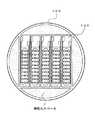
図1、図2に示すように、符号1は本発明の実施例の発光ダイオード光源装置である。この発光ダイオード光源装置1は、熱伝導性を有する基台2と、この基台2の表面に固着される薄板状の絶縁板10と、基台2の表面に実装される複数のLED素子20と、このLED素子20を封止する封止部材15などによって構成される。 As shown in FIGS. 1 and 2,
基台2はアルミ材などによって成り、表面が平坦で外形が円形である。また、絶縁板10は基台2の外形形状とほぼ等しい円形であり、BTレジンやガラスエポキシ材などによって成るプリント基板である。基台2と絶縁板10は、中心を合わせて接着剤(図示せず)などによって固着され一体化される。これにより、基台2と絶縁板10は、外形が同心の円形である。 The
絶縁板10の中央には、絶縁板10の外形と同心の円形の貫通穴13が設けられ、この貫通穴13によって基台2の中心部分の表面が露出する。この貫通穴13によって露出した領域を実装エリア14と称し、この実装エリア14に複数のLED素子20が直接実装される。よって、実装エリア14は、絶縁板10と同心の円形形状の領域である。 A circular through
また、絶縁板10の表面は銅箔などによって成る導電パターンが形成される。この導電パターンの一部として、絶縁板10の外形付近にリング状の第1の電極端子11aが形成される。また、第1の電極端子11aの内側に、同じくリング状の第2の電極端子11bが形成される。すなわち、第1の電極端子11aと第2の電極端子11bのパターン形状は共に、絶縁板10の外形と同心のリング状である。この第1、第2の電極端子11a、11bは、外部と電気的に接続して駆動電圧の供給を受ける機能を有している。 In addition, a conductive pattern made of copper foil or the like is formed on the surface of the insulating
また、絶縁板10の貫通穴13の周囲には、導電パターンの一部として、リング状の第1の接続電極12aが形成される。また、第1の接続電極12aの外側には、第2の接続電極12bが形成される。この第1の接続電極12aと第2の接続電極12bは共に、絶縁板10の外形と同心のリング状である。そして、第1の電極端子11aと第1の接続電極12aは、導電パターンの一部である接続部11cによって電気的に接続され、また、第2の電極端子11bと第2の接続電極12bは接続部11dによって電気的に接続される。 Further, a ring-shaped first connection electrode 12a is formed around the through
また、基台2の表面が露出した円形状の実装エリア14に複数のLED素子20が図示するように実装される。すなわち、3個ずつ直列に4列のLED素子20a〜20dが導電性接着剤(図示せず)等によって固着されて実装される。尚、3個直列に実装されるLED素子は区別するためにそれぞれ符号20a、20b、20c、20dと表記し、実装される全てのLED素子を指す場合は符号20と表記する。また、LED素子20の個数は限定されず、光源装置の仕様に基づいて任意に決定される。 A plurality of
次に各LED素子の接続を図1によって説明する。実装エリア14に実装されるLED素子20a〜20dは、すべて同一方向に実装され、一例として図面上左側がアノード端子(図示せず)であり、図面上右側がカソード端子(図示せず)として実装される。そして、すべてのLED素子20は、ワイヤボンダ(図示せず)によって金属細線であるワイヤ19で電気的に接続される。 Next, the connection of each LED element will be described with reference to FIG. The LED elements 20a to 20d mounted in the mounting area 14 are all mounted in the same direction. As an example, the left side of the drawing is an anode terminal (not shown), and the right side of the drawing is a cathode terminal (not shown). Is done. And all the
ここで、実装エリア14の図面上において最上列に実装される3個のLED素子20aの左側の素子は、アノード端子が接続電極12bとワイヤ19によって電気的に接続される。また、このアノード端子が接続されたLED素子20aのカソード端子と実装エリア14の中央に実装されるLED素子20aのアノード端子は、ワイヤ19によって直接接続される。また、アノード端子が接続された中央のLED素子20aのカソード端子は、実装エリア14の図面上右側に実装されるLED素子20aのアノード端子にワイヤ19によって直接接続される。そして、このアノード端子が接続された右側のLED素子20aのカソード端子は、接続電極12aとワイヤ19によって接続される。このように、3個のLED素子20aは、第1の接続電極12aと第2の接続電極12bの間で、ワイヤ19によるワイヤリングによって直列接続される。 Here, the left terminal of the three LED elements 20 a mounted in the uppermost row in the drawing of the mounting area 14 is electrically connected to the anode terminal by the connection electrode 12 b and the
また同様に、他の3列のLED素子20b、20c、20dにおいても、第1の接続電極12aと第2の接続電極12bの間で、ワイヤ19によるワイヤリングによって直列接続される。このように、実装エリア14に実装されるLED素子20a〜20dは、ワイヤ19によって3個が直列接続され、この直列接続された4つのグループが、第1の接続電極12aと第2の接続電極12bの間で、並列接続される構成となる。ここで、実装エリア14は狭い領域であるが、この中に合計12個のLED素子20を実装して接続できる理由は、隣り同士のLED素子20をワイヤ19によって直接ワイヤリングすることで、実装密度を高めているからである。尚、LED素子20a〜20dの配線の詳細は後述する。 Similarly, in the other three rows of
また、図2に示す封止部材15は、実装エリア14に実装される複数のLED素子20とワイヤ19とを封止するが、リング状のダム材16の内側に充填され硬化される。この封止部材15はLED素子20の発光を外部に出射するために透光性を有する樹脂によって成る。また、ダム材16は薄いリング状で、シリコーンに酸化チタンを混合した成分であり、絶縁板10の略中央の表面に固着される。このダム材16の内側の円形領域、すなわち、封止部材15が充填された領域からLED素子20の出射光が外部に発光するので、この円形領域を発光エリア21と称する。 Further, the sealing member 15 shown in FIG. 2 seals the plurality of
この発光エリア21は、絶縁板10の外形と同心であることが好ましい。尚、図1の封止部材15とダム材16は、説明を分かりやすくするために図示を省略し、発光エリア21の円外形のみを記載している。また、ダム材16は、封止部材15の硬化後に取り除いても良く、また、ダム材16を用いずに封止部材15を充填/硬化しても良い。 The
[本発明の発光ダイオード光源装置のLED素子の接続回路の説明:図3]
次に、本発明の実施例の発光ダイオード光源装置のLED素子の接続回路の詳細を図3に基づいて説明する。図3に示すように、本発明の実施例の発光ダイオード光源装置のLED素子20は、前述したように、3個直列のLED素子のグループが4列並列に接続されている。詳しくは、LED素子20aの3個が直列接続されたグループGaと、LED素子20bの3個が直列接続されたグループGbと、LED素子20cの3個が直列接続されたグループGc、及びLED素子20dの3個が直列接続されたグループGdの4つのグループによって構成される。そして、各グループのLED素子20a〜20dは、前述したように第1の接続電極12aと第2の接続電極12bの間で並列接続される(図1参照)。[Description of LED Element Connection Circuit of Light Emitting Diode Light Source Device of the Present Invention: FIG. 3]
Next, details of the connection circuit of the LED elements of the light-emitting diode light source device according to the embodiment of the present invention will be described with reference to FIG. As shown in FIG. 3, as described above, the
そして、第1の接続電極12aは第1の電極端子11aに接続され、第2の接続電極12bは、第2の電極端子11bに接続されているので、図3に示すように、各グループGa〜GdのLED素子20a〜20dは、第1の電極端子11aと第2の電極端子11bの間で並列に接続される。 Since the first connection electrode 12a is connected to the first electrode terminal 11a and the second connection electrode 12b is connected to the second electrode terminal 11b, as shown in FIG. -Gd LED elements 20a-20d are connected in parallel between the first electrode terminal 11a and the second electrode terminal 11b.
これにより、電極端子11a、11bに所定の駆動電圧を印加するならば、全てのグループGa〜Gdに駆動電流が流れて、全てのLED素子20を点灯させることが出来る。ここで、直列接続されている各グループGa〜Gdの個々のLED素子には、当然であるが等しい値の駆動電流が流れるので、グループ内のLED素子の駆動条件は等しい。
また、各グループGa〜Gdは、3個のLED素子が直列接続されているので、個々のLED素子の特性ばらつきが平均化され、各グループGa〜Gdには、ほぼ等しい駆動電流が流れる。Thereby, if a predetermined drive voltage is applied to the electrode terminals 11a and 11b, a drive current flows through all the groups Ga to Gd, and all the
Moreover, since three LED elements are connected in series in each group Ga to Gd, characteristic variations of the individual LED elements are averaged, and substantially equal drive currents flow in each group Ga to Gd.
このように、本発明の発光ダイオード光源装置は、多数のLED素子を実装して駆動するが、隣接する素子間をワイヤリングによって直列接続し、この直列接続のグループを並列接続する基本構成を採用している。この結果、LED素子は多数であっても、各LED素子の駆動条件がほぼ等しくなるので、LED素子間の光量ばらつきが抑制されて、発光パターンに偏りや乱れ等が少ない発光ダイオード光源装置を実現することが出来る。 As described above, the light-emitting diode light source device of the present invention is driven by mounting a large number of LED elements, and adopts a basic configuration in which adjacent elements are connected in series by wiring and this group of series connections is connected in parallel. ing. As a result, even if there are a large number of LED elements, the driving conditions of the LED elements are almost equal, so the variation in the amount of light between the LED elements is suppressed, and a light-emitting diode light source device with less bias or disturbance in the light emission pattern is realized. I can do it.
ここで、多数のLED素子の全てを直列接続するならば、全てのLED素子に同一の駆動電流が流れるので、駆動条件を一致させて個々のLED素子の発光ばらつきを抑制できる。しかし、多数のLED素子を直列接続すると駆動電圧が高圧となるので、特殊な駆動回路が必要となり、経済性や安全性に問題がある。また、すべてのLED素子を並列接続するならば、駆動電圧は低電圧でよいが、LED素子の電気的な特性ばらつきによって、個々のLED素子に流れる駆動電流が大きく異なることになり、大きな発光ばらつきが生じる問題がある。 Here, if all of the many LED elements are connected in series, the same drive current flows through all the LED elements, so that the drive conditions are matched to suppress the light emission variation of the individual LED elements. However, when a large number of LED elements are connected in series, the drive voltage becomes high, so a special drive circuit is required, and there is a problem in economy and safety. Moreover, if all LED elements are connected in parallel, the drive voltage may be low, but the drive currents flowing through the individual LED elements vary greatly due to variations in the electrical characteristics of the LED elements, resulting in large variations in light emission. There is a problem that occurs.
このように、LED素子の接続は、直列接続、並列接続の両方に問題があるが、本発明は多数のLED素子を所定の数でグループ分けし、直列接続と並列接続を混合することで、駆動電圧の高電圧化を防ぐと共に、個々のLED素子の光量ばらつきを抑制できる優れた効果を備えている。尚、本実施例においては、直列数が3個であり、並列数が4列であるが、LED素子の直並列の構成は限定されるものではなく、発光ダイオード光源装置の仕様に基づいて任意に決定される。 Thus, the connection of LED elements has a problem in both series connection and parallel connection, but the present invention groups a large number of LED elements in a predetermined number, and mixes the series connection and the parallel connection. While preventing the drive voltage from becoming high, it has an excellent effect of suppressing the variation in light quantity of individual LED elements. In the present embodiment, the number of series is three and the number of parallel is four rows, but the series-parallel configuration of the LED elements is not limited, and is arbitrary based on the specifications of the light-emitting diode light source device. To be determined.
[本発明の発光ダイオード光源装置の照明装置への組み込み例の説明:図4]
次に本発明の発光ダイオード光源装置を照明装置に組み込む場合の一例を図4に基づいて説明する。図4に示すように、30は電球型の照明装置であり、説明の都合上、内部を透過して示しており、また、説明する上での不要な部品は図示を省略している。この電球型の照明装置30は略球形の発光部31と、この発光部31を支持する略円筒形の支持部32によって構成される。[Description of Example of Incorporating Light-Emitting Diode Light Source Device of the Present Invention into Lighting Device: FIG. 4]
Next, an example of incorporating the light-emitting diode light source device of the present invention into a lighting device will be described with reference to FIG. As shown in FIG. 4,
ここで、支持部32には二つの電極材33a、33bが配設されている。この電極材33aの先端は支持部32の中心から発光ダイオード光源装置1の第1の電極端子11aの中央部半径と同一距離の位置に配設され、また、電極材33bの先端は支持部32の中心から発光ダイオード光源装置1の第2の電極端子11bの中央部半径と同一距離の位置に配設される。 Here, two electrode members 33 a and 33 b are disposed on the
この構成によって、本発明の実施例の発光ダイオード光源装置1が、支持部32の下面部32a側から矢印Aの方向に挿入されるならば、支持部32の電極材33a、33bに発光ダイオード光源装置1の第1、第2の電極端子11a、11bがそれぞれ接して、電極材33aと第1の電極端子11aが電気的に接続され、電極材33bと第2の電極端子11bが電気的に接続される。そして、電気的に接続された位置で、発光ダイオード光源装置1は図示しない支持部32の固定部材によって固定される。 With this configuration, if the light-emitting diode
ここで、発光ダイオード光源装置1の第1、第2の電極端子11a、11bは、前述したように、絶縁板10の外形と同心のリング状に形成されているので、発光ダイオード光源装置1が支持部32に対して、いろいろな回転方向で組み込まれても、支持部32の電極材33a、33bと発光ダイオード光源装置1の第1、第2の電極端子11a、11bの位置関係がずれることはないので、接続不良になったり、また、二つの接続が逆になったりすることはない。 Here, since the first and second electrode terminals 11a and 11b of the light-emitting diode
また、発光ダイオード光源装置1は、支持部32の内部で回転させながら固定しても良い。すなわち、実施例の発光ダイオード光源装置1が、支持部32の下面部32a側から矢印Aの方向に挿入され、電極材33a、33bに発光ダイオード光源装置1の第1、第2の電極端子11a、11bが接する位置で、一例として矢印Bの方向に約90度回転して、図示しない固定部材によって固定する。 The light-emitting diode
ここで、発光ダイオード光源装置1の第1、第2の電極端子11a、11bは、前述したように、絶縁板10の外形と同心のリング状に形成されているので、発光ダイオード光源装置1が支持部32の内部で回転しながら固定されても、第1、第2の電極端子11a、11bは照明装置30の電極材33a、33bに対して位置ずれを起こすことが無く、確実に電気的接続を行うことが出来る。すなわち、発光ダイオード光源装置1が支持部32の内部で矢印Bの方向に回転すると、電極材33a、33bがリング状の第1、第2の電極端子11a、11bの上を滑るようにして移動し、発光ダイオード光源装置1の固定によって、電極材33a、33bは第1、第2の電極端子11a、11bのパターン上で確実に電気的な接続を保持した状態で停止する。 Here, since the first and second electrode terminals 11a and 11b of the light-emitting diode
また、発光ダイオード光源装置1を固定するための回転量は限定されず、例えば180度程度回転したとしても、電極材33a、33bと第1、第2の電極端子11a、11bの位置関係はずれないので、確実に電気的な接続を保持することが出来る。また、発光ダイオード光源装置1を支持部32に組み込んだ後に、支持部32の下面部32aに、外部と電気的接続を取るための外部電極端子が取り付けられているが、ここでの説明は省略する。 Further, the amount of rotation for fixing the light-emitting diode
このように、本発明の発光ダイオード光源装置の第1、第2の電極端子11a、11bは、絶縁板10の外形と同心のリング状であるので、発光ダイオード光源装置1がいろいろな回転方向で照明装置30に組み込まれても、照明装置30との電気的な接続を容易、且つ、確実に行うことが出来、発光ダイオード光源装置の組み込みが簡単で信頼性に優れた照明装置を得ることが出来る。尚、本発明の発光ダイオード光源装置を組み込む照明装置は電球型に限定されず、どのような形態の照明装置に対しても組み込むことが出来る。 Thus, since the first and second electrode terminals 11a and 11b of the light-emitting diode light source device of the present invention have a ring shape concentric with the outer shape of the insulating
[本発明の発光ダイオード光源装置の動作の説明:図5]
次に、本発明の発光ダイオード光源装置の動作の一例を図5に基づいて説明する。図5に示すように、本発明の実施例の発光ダイオード光源装置1が照明装置30(図4参照)に組み込まれ、外部の駆動電源36が照明装置30に内蔵される電極材33aと33bに接続されると、本発明の発光ダイオード光源装置1の第1、第2の電極端子11a、11bに電極材33a、33bを介して駆動電流Iが流れ、発光ダイオード光源装置1のすべてのLED素子20(図1参照)は点灯し、出射光L1を出射する。[Description of Operation of Light Emitting Diode Light Source Device of the Present Invention: FIG. 5]
Next, an example of operation | movement of the light-emitting-diode light source device of this invention is demonstrated based on FIG. As shown in FIG. 5, the light-emitting diode
この出射光L1は発光ダイオード光源装置1の発光エリア21が円形であるので、略円形状の発光パターンP1(破線で示す)として拡散しながら出射されるが、発光エリア21の上部に所定の距離を置いて照明装置30の内部に組み込まれているレンズ35によって集光され、このレンズ35から集光された出射光L2が出射される。このように、本発明の発光ダイオード光源装置1は、狭い円形の発光エリア21から集光しやすい良好な発光パターンの出射光L1を出射することが出来るので、この出射光L1を集光するためのレンズ35などの光学設計が容易であり、ルーメンデンシティが高く、小型で集光力に優れた高輝度高出力の光源装置を提供することが出来る。尚、レンズ35は集光レンズに限定されず、出射光L1を拡散する拡散型レンズでも良く、また、レンズ35が無くても良い。 Since the
[本発明の発光ダイオード光源装置に放熱部材を取り付ける説明:図6]
次に、本発明の発光ダイオード光源装置に放熱部材を取り付けた構成を図6に基づいて説明する。図6に示すように、発光ダイオード光源装置1の基台2の底面、すなわち、基台2の実装エリア14(図1参照)の反対面に、放熱部材としてのヒートシンク27を固着して取り付ける。また、基台2とヒートシンク27の隙間には、熱伝導性のシリコーン28を塗布すると良い。また、図示しないが取り付けを確実にするために、発光ダイオード光源装置1とヒートシンク27をネジ等によって固定しても良い。[Description of attaching a heat dissipation member to the light emitting diode light source device of the present invention: FIG. 6]
Next, the structure which attached the heat radiating member to the light emitting diode light source device of this invention is demonstrated based on FIG. As shown in FIG. 6, a heat sink 27 as a heat radiating member is fixedly attached to the bottom surface of the
この構成により、発光ダイオード光源装置1は、多数のLED素子20(図1参照)が実装されているが、このLED素子20は、基台2の表面に直接実装されているので、LED素子20からの発熱は熱伝導性の基台2に効率良く伝わり、更にヒートシンク27に低い熱抵抗で伝達されるので、LED素子20の発熱を効率よく放熱することが出来る。この結果、LED素子20の温度上昇が抑制され、長寿命で信頼性に優れた高輝度高出力の発光ダイオード光源装置を提供することが出来る。尚、ヒートシンク27は、発光ダイオード光源装置1と同程度の大きさとして示したが、ヒートシンク27の外形は限定されず、発光ダイオード光源装置1より外形の大きなヒートシンクを取り付けて、更に放熱効率を高めても良い。 With this configuration, the light-emitting diode
[本発明の発光ダイオード光源装置を組み込んだ照明装置の概略説明:図7]
次に本発明の発光ダイオード光源装置を組み込んだ照明装置の一例を図7によって説明する。ここで、図7(a)は電球型の照明装置の透視側面図であり、図7(b)は電球型の照明装置の透視上面図である。図7(a)及び図7(b)に示すように、電球型の照明装置30は、前述したように、発光部31と支持部32によって構成され、本発明の発光ダイオード光源装置1は、支持部32の内部に、図示しない固定部材によって固定され組み込まれている。[Schematic Description of Lighting Device Incorporating Light Emitting Diode Light Source Device of the Present Invention: FIG. 7]
Next, an example of a lighting device incorporating the light-emitting diode light source device of the present invention will be described with reference to FIG. Here, FIG. 7A is a see-through side view of the bulb-type illumination device, and FIG. 7B is a see-through top view of the bulb-type illumination device. As shown in FIGS. 7 (a) and 7 (b), the light bulb-
また、発光ダイオード光源装置1は、前述のヒートシンク27が取り付けられ、放熱効果を高めているが、ヒートシンク27はなくても良い。37は支持部32の下面部に取り付けられる外部電極端子であり、この外部電極端子37を介して外部電源の供給を受ける。駆動電源36は外部電極端子37から外部電源の供給を受け、発光ダイオード光源装置1を駆動するために必要な直流の駆動電圧を生成し、電極材33a、33bを介して発光ダイオード光源装置1に駆動電圧を供給する。また、発光ダイオード光源装置1の出射方向には、前述したレンズ35が配設されている。 Further, the light-emitting diode
ここで、図示する電球型の照明装置30のように外形の断面が円形である照明装置が一般的であるが、このような照明装置に従来例のような四角形のLED光源装置を組み込むと、照明装置内部のスペース効率が悪いので照明装置が大型化しやすくなり、また、光源装置の基台面積が狭くなるので放熱能力が低下して高出力化出来ないなどの問題がある。しかしながら、本発明の発光ダイオード光源装置のように外形が円形状であれば、図7(b)で示すように照明装置30の支持部32の内部に無駄なスペースが無く、スペースを有効に使用出来る。これにより、放熱板の機能を有する基台2、及び放熱効果を高めるヒートシンク27の面積を最大限に広く確保して、小型でありながら放熱特性に優れた高輝度高出力の発光ダイオード光源装置を提供することが出来る。 Here, a lighting device having a circular outer cross section, such as a light bulb-
また、本発明の発光ダイオード光源装置の外形が円形状であるので、電球型の照明装置に組み込みやすく、構造が簡単な照明装置を実現することが出来る。また、本発明の発光ダイオード光源装置は外形が円形状であると共に、実装エリア14と発光エリア21も円形状であるので、出射光が略円形状の発光パターンとして出射され、レンズなどの光学設計を容易に行うことが出来る。また、出射光の発光パターンが略円形状であるので、発光ダイオード光源装置1が照明装置にどのような回転角度で組み込まれたとしても発光パターンがほとんど変化せず、発光特性のばらつきが少ない照明装置を提供することが出来る。 In addition, since the outer shape of the light-emitting diode light source device of the present invention is circular, it is easy to incorporate into a light bulb-type lighting device, and a lighting device with a simple structure can be realized. In addition, since the outer shape of the light-emitting diode light source device of the present invention is circular, and the mounting area 14 and the light-emitting
尚、本発明の実施例で示した正面図、側面図等は、これに限定されるものではなく、本発明の要旨を満たすものであれば、任意に変更してよい。 The front view, the side view, and the like shown in the embodiments of the present invention are not limited to this, and may be arbitrarily changed as long as they satisfy the gist of the present invention.
本発明の発光ダイオード光源装置は、小型でルーメンデンシティの高い光源装置を実現できるので、一般用途の照明用光源、車載用光源など、照明用光源装置として幅広く利用することが出来る。 Since the light-emitting diode light source device of the present invention can realize a light source device having a small size and high lumen density, it can be widely used as an illumination light source device such as a general-purpose illumination light source and an in-vehicle light source.
1 発光ダイオード光源装置
2 基台
10 絶縁板
11a、11b 電極端子
11c、11d 接続部
12a、12b 接続電極
13 実装穴
14 実装エリア
15 封止部材
16 ダム材
19 ワイヤ
20、20a、20b、20c、20d LED素子
21 発光エリア
27 ヒートシンク
28 シリコーン
30 照明装置
31 発光部
32 支持部
32a 下面部
33a、33b 電極材
35 レンズ
36 駆動電源
37 外部電極端子
Ga、Gb、Gc、Gd グループ
L1、L2 出射光
P1 発光パターンDESCRIPTION OF
Claims (5)
Translated fromJapanese前記基台と前記絶縁板の外形は円形であり、前記貫通穴は前記絶縁板の外形と同心の円形であり、
前記絶縁板の導電パターンの一部は、外部と電気的に接続するために前記絶縁板の外形と同心の略リング状の電極端子が形成されることを特徴とする発光ダイオード光源装置。A base having thermal conductivity, an insulating plate formed with a conductive pattern on the surface and fixed to the surface of the base, and mounting of the base surface exposed by a through hole provided in a part of the insulating plate With a plurality of light emitting diode elements mounted in the area,
The base and the outer shape of the insulating plate are circular, and the through hole is a concentric circle with the outer shape of the insulating plate,
A part of the conductive pattern of the insulating plate is formed with a substantially ring-shaped electrode terminal concentric with the outer shape of the insulating plate for electrical connection with the outside.
The light emitting diode light source device according to claim 1, wherein a heat radiating member is attached to the base on the opposite surface of the mounting area to enhance a heat radiating effect.
Priority Applications (2)
| Application Number | Priority Date | Filing Date | Title |
|---|---|---|---|
| JP2009170453AJP5431818B2 (en) | 2009-07-21 | 2009-07-21 | Light emitting diode light source device |
| US12/840,800US8154037B2 (en) | 2009-07-21 | 2010-07-21 | Light-emitting diode light source apparatus |
Applications Claiming Priority (1)
| Application Number | Priority Date | Filing Date | Title |
|---|---|---|---|
| JP2009170453AJP5431818B2 (en) | 2009-07-21 | 2009-07-21 | Light emitting diode light source device |
Publications (2)
| Publication Number | Publication Date |
|---|---|
| JP2011028864A JP2011028864A (en) | 2011-02-10 |
| JP5431818B2true JP5431818B2 (en) | 2014-03-05 |
Family
ID=43497191
Family Applications (1)
| Application Number | Title | Priority Date | Filing Date |
|---|---|---|---|
| JP2009170453AActiveJP5431818B2 (en) | 2009-07-21 | 2009-07-21 | Light emitting diode light source device |
Country Status (2)
| Country | Link |
|---|---|
| US (1) | US8154037B2 (en) |
| JP (1) | JP5431818B2 (en) |
Families Citing this family (30)
| Publication number | Priority date | Publication date | Assignee | Title |
|---|---|---|---|---|
| US20100226139A1 (en) | 2008-12-05 | 2010-09-09 | Permlight Products, Inc. | Led-based light engine |
| CN102292834A (en)* | 2008-12-15 | 2011-12-21 | 因西亚瓦(控股)有限公司 | Silicon light emitting device utilising reach-through effects |
| JP5343040B2 (en)* | 2010-06-07 | 2013-11-13 | 株式会社東芝 | Semiconductor light emitting device |
| US9490235B2 (en)* | 2010-11-22 | 2016-11-08 | Cree, Inc. | Light emitting devices, systems, and methods |
| JP5836780B2 (en)* | 2011-12-02 | 2015-12-24 | 日立アプライアンス株式会社 | Light emitting diode module and lighting apparatus using the same |
| JP6015004B2 (en)* | 2012-01-05 | 2016-10-26 | 日亜化学工業株式会社 | LIGHT EMITTING DEVICE AND LIGHT EMITTING DEVICE MANUFACTURING METHOD |
| US8847251B2 (en) | 2012-03-13 | 2014-09-30 | Panasonic Corporation | Substrate, light-emitting device, and lighting apparatus having a largest gap between two lines at light-emitting element mounting position |
| JP5934836B2 (en) | 2012-04-04 | 2016-06-15 | アルカテル−ルーセント | System and method for data plane alive separation of label distribution protocol (LDP) label switched path (LSP) |
| DE102012103983A1 (en)* | 2012-05-07 | 2013-11-07 | Vossloh-Schwabe Optoelectronic Gmbh & Co. Kg | Light-emitting diode arrangement, in particular for illumination purposes, and method for producing a light-emitting diode arrangement |
| EP2878883A4 (en)* | 2012-07-25 | 2015-11-25 | Panasonic Ip Man Co Ltd | LIGHT EMITTING MODULE |
| US9194576B2 (en)* | 2013-06-04 | 2015-11-24 | Component Hardware Group, Inc. | LED bulb with heat sink |
| US9781801B2 (en)* | 2014-01-06 | 2017-10-03 | Dell Products, Lp | Performance lighting and control method |
| KR101567437B1 (en)* | 2014-01-28 | 2015-11-09 | 유창운 | Led lighting apparatus for entertainment establishment |
| KR102145919B1 (en)* | 2014-05-30 | 2020-08-19 | 엘지이노텍 주식회사 | A light emitting device package |
| USD751045S1 (en)* | 2014-06-16 | 2016-03-08 | Citizen Electronics Co., Ltd. | Light emitting diode |
| USD751517S1 (en) | 2014-06-16 | 2016-03-15 | Citizen Electronics Co., Ltd. | Light emitting diode |
| USD751046S1 (en)* | 2014-06-16 | 2016-03-08 | Citizen Electronics Co., Ltd. | Light emitting diode |
| CN104121504A (en)* | 2014-06-30 | 2014-10-29 | 李祖国 | LED lamp with improved circuit board and manufacturing method of circuit board of LED lamp |
| CN107148734B (en)* | 2015-09-18 | 2019-04-05 | 株式会社安川电机 | The state display device and power inverter of industrial machine |
| JP6869000B2 (en)* | 2015-10-23 | 2021-05-12 | シチズン電子株式会社 | Luminous module |
| KR101987196B1 (en)* | 2016-06-14 | 2019-06-11 | 삼성디스플레이 주식회사 | Pixel structure, display apparatus including the pixel structure and method of manufacturing the same |
| FR3062953A1 (en)* | 2017-02-15 | 2018-08-17 | Commissariat A L'energie Atomique Et Aux Energies Alternatives | DEVICE COMPRISING A PLURALITY OF DIODES |
| DE102017208973A1 (en)* | 2017-05-29 | 2018-11-29 | Osram Gmbh | ELECTRONIC ASSEMBLY FOR LIGHTING APPLICATIONS, LIGHTING DEVICE AND METHOD FOR PRODUCING AN ELECTRONIC MODULE |
| DE102018211723A1 (en)* | 2018-07-13 | 2020-01-16 | Osram Gmbh | LED ARRANGEMENT AND LIGHTING DEVICE |
| KR102091810B1 (en)* | 2019-06-03 | 2020-03-23 | 삼성디스플레이 주식회사 | Pixel Structure And Display Apparatus Including The Same |
| KR102430815B1 (en)* | 2019-06-03 | 2022-08-10 | 삼성디스플레이 주식회사 | Pixel Structure And Display Apparatus Including The Same |
| KR102825980B1 (en) | 2019-12-12 | 2025-06-27 | 삼성디스플레이 주식회사 | Display device |
| KR102698236B1 (en) | 2019-12-16 | 2024-08-23 | 삼성디스플레이 주식회사 | Display device |
| KR102847336B1 (en)* | 2020-07-28 | 2025-08-18 | 삼성디스플레이 주식회사 | Display device |
| CN117239043B (en)* | 2023-11-16 | 2024-02-27 | 江西鸿利光电有限公司 | Light-emitting device and preparation method thereof |
Family Cites Families (11)
| Publication number | Priority date | Publication date | Assignee | Title |
|---|---|---|---|---|
| DE10229067B4 (en)* | 2002-06-28 | 2007-08-16 | Osram Opto Semiconductors Gmbh | Optoelectronic component and method for its production |
| DE10392736T5 (en)* | 2002-10-25 | 2005-07-07 | Moriyama Sangyo K.K. | light module |
| US6999318B2 (en)* | 2003-07-28 | 2006-02-14 | Honeywell International Inc. | Heatsinking electronic devices |
| JP4241658B2 (en) | 2005-04-14 | 2009-03-18 | シチズン電子株式会社 | Light emitting diode light source unit and light emitting diode light source formed using the same |
| JP5066333B2 (en)* | 2005-11-02 | 2012-11-07 | シチズン電子株式会社 | LED light emitting device. |
| DE102006048230B4 (en)* | 2006-10-11 | 2012-11-08 | Osram Ag | Light-emitting diode system, method for producing such and backlighting device |
| JP2008124008A (en)* | 2006-10-18 | 2008-05-29 | Nobuichi Tsubota | Led unit, manufacturing method of led unit, and luminaire for ceiling using led unit |
| JP2009009926A (en)* | 2007-03-23 | 2009-01-15 | Toshiba Lighting & Technology Corp | Light emitting diode lighting device |
| JP5145895B2 (en)* | 2007-07-04 | 2013-02-20 | 東芝ライテック株式会社 | Lighting device |
| TW200923262A (en)* | 2007-11-30 | 2009-06-01 | Tysun Inc | High heat dissipation optic module for light emitting diode and its manufacturing method |
| JP2009140717A (en)* | 2007-12-05 | 2009-06-25 | Toshiba Lighting & Technology Corp | Lighting device |
- 2009
- 2009-07-21JPJP2009170453Apatent/JP5431818B2/enactiveActive
- 2010
- 2010-07-21USUS12/840,800patent/US8154037B2/enactiveActive
Also Published As
| Publication number | Publication date |
|---|---|
| JP2011028864A (en) | 2011-02-10 |
| US20110019420A1 (en) | 2011-01-27 |
| US8154037B2 (en) | 2012-04-10 |
Similar Documents
| Publication | Publication Date | Title |
|---|---|---|
| JP5431818B2 (en) | Light emitting diode light source device | |
| CN101930972B (en) | LED device | |
| JP4241658B2 (en) | Light emitting diode light source unit and light emitting diode light source formed using the same | |
| JP4932064B2 (en) | Light emitting module, light source device, liquid crystal display device, and method for manufacturing light emitting module | |
| US7642704B2 (en) | Light-emitting diode with a base | |
| JP6869000B2 (en) | Luminous module | |
| EP2342760B1 (en) | Efficient led array | |
| JP2005158957A (en) | Light emitting device | |
| JP6056213B2 (en) | Light emitting module and lighting device | |
| JP5705323B2 (en) | High power LED light source structure with improved heat dissipation characteristics | |
| JP2014082481A (en) | Light emitting device | |
| KR100873458B1 (en) | LED module for lighting | |
| KR20080088140A (en) | Heat dissipation substrate and light emitting device including the same | |
| US20150009662A1 (en) | Light-Emitting Module and Luminaire | |
| JP5845053B2 (en) | LED lamp | |
| JP2014192313A (en) | LED light-emitting device | |
| JPWO2014013671A1 (en) | Light bulb shaped lamp and lighting device | |
| JP2006319290A (en) | Light emitting diode light source unit and valve type thereof | |
| JP2009289441A (en) | Led lamp, and manufacturing method thereof | |
| JP2014183200A (en) | Light-emitting device and led lighting equipment | |
| WO2014030275A1 (en) | Light bulb-shaped lamp and lighting device | |
| JP2012134306A (en) | Light-emitting device and luminaire using the same | |
| JPWO2014013672A1 (en) | Light bulb shaped lamp and lighting device | |
| JP2011243709A (en) | Light-emitting module and lighting apparatus equipped with the same | |
| KR20150035620A (en) | Chip on board light emitting diode |
Legal Events
| Date | Code | Title | Description |
|---|---|---|---|
| A621 | Written request for application examination | Free format text:JAPANESE INTERMEDIATE CODE: A621 Effective date:20120523 | |
| A977 | Report on retrieval | Free format text:JAPANESE INTERMEDIATE CODE: A971007 Effective date:20130610 | |
| A131 | Notification of reasons for refusal | Free format text:JAPANESE INTERMEDIATE CODE: A131 Effective date:20130618 | |
| A521 | Request for written amendment filed | Free format text:JAPANESE INTERMEDIATE CODE: A523 Effective date:20130726 | |
| TRDD | Decision of grant or rejection written | ||
| A01 | Written decision to grant a patent or to grant a registration (utility model) | Free format text:JAPANESE INTERMEDIATE CODE: A01 Effective date:20131203 | |
| A61 | First payment of annual fees (during grant procedure) | Free format text:JAPANESE INTERMEDIATE CODE: A61 Effective date:20131205 | |
| R150 | Certificate of patent or registration of utility model | Free format text:JAPANESE INTERMEDIATE CODE: R150 Ref document number:5431818 Country of ref document:JP Free format text:JAPANESE INTERMEDIATE CODE: R150 | |
| S533 | Written request for registration of change of name | Free format text:JAPANESE INTERMEDIATE CODE: R313533 | |
| R350 | Written notification of registration of transfer | Free format text:JAPANESE INTERMEDIATE CODE: R350 | |
| R250 | Receipt of annual fees | Free format text:JAPANESE INTERMEDIATE CODE: R250 | |
| R250 | Receipt of annual fees | Free format text:JAPANESE INTERMEDIATE CODE: R250 | |
| R250 | Receipt of annual fees | Free format text:JAPANESE INTERMEDIATE CODE: R250 | |
| R250 | Receipt of annual fees | Free format text:JAPANESE INTERMEDIATE CODE: R250 | |
| R250 | Receipt of annual fees | Free format text:JAPANESE INTERMEDIATE CODE: R250 |