JP5430671B2 - Lead wire with high surface resistance - Google Patents
Lead wire with high surface resistanceDownload PDFInfo
- Publication number
- JP5430671B2 JP5430671B2JP2011539494AJP2011539494AJP5430671B2JP 5430671 B2JP5430671 B2JP 5430671B2JP 2011539494 AJP2011539494 AJP 2011539494AJP 2011539494 AJP2011539494 AJP 2011539494AJP 5430671 B2JP5430671 B2JP 5430671B2
- Authority
- JP
- Japan
- Prior art keywords
- lead
- conductor
- resistive
- coil
- medical device
- Prior art date
- Legal status (The legal status is an assumption and is not a legal conclusion. Google has not performed a legal analysis and makes no representation as to the accuracy of the status listed.)
- Expired - Fee Related
Links
- WABPQHHGFIMREM-UHFFFAOYSA-Nlead(0)Chemical compound[Pb]WABPQHHGFIMREM-UHFFFAOYSA-N0.000titleclaimsdescription21
- 239000004020conductorSubstances0.000claimsdescription181
- 238000002595magnetic resonance imagingMethods0.000claimsdescription46
- 239000000463materialSubstances0.000claimsdescription25
- 239000011248coating agentSubstances0.000claimsdescription17
- 238000000576coating methodMethods0.000claimsdescription17
- 239000012212insulatorSubstances0.000description37
- 238000010438heat treatmentMethods0.000description7
- 238000000034methodMethods0.000description7
- BQCADISMDOOEFD-UHFFFAOYSA-NSilverChemical compound[Ag]BQCADISMDOOEFD-UHFFFAOYSA-N0.000description6
- 229910052709silverInorganic materials0.000description6
- 239000004332silverSubstances0.000description6
- 230000008859changeEffects0.000description4
- 230000007423decreaseEffects0.000description4
- 230000003247decreasing effectEffects0.000description4
- 230000005684electric fieldEffects0.000description4
- 239000011810insulating materialSubstances0.000description4
- 229910052751metalInorganic materials0.000description3
- 239000002184metalSubstances0.000description3
- 238000012986modificationMethods0.000description3
- 230000004048modificationEffects0.000description3
- 239000002245particleSubstances0.000description3
- 239000008280bloodSubstances0.000description2
- 210000004369bloodAnatomy0.000description2
- 230000000747cardiac effectEffects0.000description2
- 229920001940conductive polymerPolymers0.000description2
- 238000010276constructionMethods0.000description2
- 230000008878couplingEffects0.000description2
- 238000010168coupling processMethods0.000description2
- 238000005859coupling reactionMethods0.000description2
- 238000010586diagramMethods0.000description2
- 230000002500effect on skinEffects0.000description2
- 239000000945fillerSubstances0.000description2
- 238000003384imaging methodMethods0.000description2
- 238000002513implantationMethods0.000description2
- 238000010899nucleationMethods0.000description2
- 229920001296polysiloxanePolymers0.000description2
- 229920002635polyurethanePolymers0.000description2
- 239000004814polyurethaneSubstances0.000description2
- 210000005245right atriumAnatomy0.000description2
- 210000005241right ventricleAnatomy0.000description2
- 230000035939shockEffects0.000description2
- 230000001225therapeutic effectEffects0.000description2
- 229910052582BNInorganic materials0.000description1
- PZNSFCLAULLKQX-UHFFFAOYSA-NBoron nitrideChemical compoundN#BPZNSFCLAULLKQX-UHFFFAOYSA-N0.000description1
- OKTJSMMVPCPJKN-UHFFFAOYSA-NCarbonChemical compound[C]OKTJSMMVPCPJKN-UHFFFAOYSA-N0.000description1
- 238000005481NMR spectroscopyMethods0.000description1
- 208000001871TachycardiaDiseases0.000description1
- 210000001015abdomenAnatomy0.000description1
- 238000010521absorption reactionMethods0.000description1
- 238000007792additionMethods0.000description1
- 230000000059bradycardiac effectEffects0.000description1
- 229910052799carbonInorganic materials0.000description1
- 239000002131composite materialSubstances0.000description1
- 230000000694effectsEffects0.000description1
- 230000005670electromagnetic radiationEffects0.000description1
- 238000001827electrotherapyMethods0.000description1
- 210000005246left atriumAnatomy0.000description1
- 210000005240left ventricleAnatomy0.000description1
- 150000002739metalsChemical class0.000description1
- 208000010125myocardial infarctionDiseases0.000description1
- TWNQGVIAIRXVLR-UHFFFAOYSA-Noxo(oxoalumanyloxy)alumaneChemical compoundO=[Al]O[Al]=OTWNQGVIAIRXVLR-UHFFFAOYSA-N0.000description1
- 229920000553poly(phenylenevinylene)Polymers0.000description1
- 229920002098polyfluorenePolymers0.000description1
- -1polyphenylene vinylenePolymers0.000description1
- 230000008569processEffects0.000description1
- 238000012887quadratic functionMethods0.000description1
- 230000004044responseEffects0.000description1
- 230000003068static effectEffects0.000description1
- 230000006794tachycardiaEffects0.000description1
- 210000003462veinAnatomy0.000description1
- 238000004804windingMethods0.000description1
Images


Classifications
- A—HUMAN NECESSITIES
- A61—MEDICAL OR VETERINARY SCIENCE; HYGIENE
- A61N—ELECTROTHERAPY; MAGNETOTHERAPY; RADIATION THERAPY; ULTRASOUND THERAPY
- A61N1/00—Electrotherapy; Circuits therefor
- A61N1/02—Details
- A61N1/04—Electrodes
- A61N1/05—Electrodes for implantation or insertion into the body, e.g. heart electrode
- A61N1/056—Transvascular endocardial electrode systems
- A—HUMAN NECESSITIES
- A61—MEDICAL OR VETERINARY SCIENCE; HYGIENE
- A61N—ELECTROTHERAPY; MAGNETOTHERAPY; RADIATION THERAPY; ULTRASOUND THERAPY
- A61N1/00—Electrotherapy; Circuits therefor
- A61N1/18—Applying electric currents by contact electrodes
- A61N1/32—Applying electric currents by contact electrodes alternating or intermittent currents
- A61N1/36—Applying electric currents by contact electrodes alternating or intermittent currents for stimulation
- A61N1/362—Heart stimulators
- A61N1/37—Monitoring; Protecting
- A61N1/3718—Monitoring of or protection against external electromagnetic fields or currents
- A—HUMAN NECESSITIES
- A61—MEDICAL OR VETERINARY SCIENCE; HYGIENE
- A61N—ELECTROTHERAPY; MAGNETOTHERAPY; RADIATION THERAPY; ULTRASOUND THERAPY
- A61N1/00—Electrotherapy; Circuits therefor
- A61N1/02—Details
- A61N1/08—Arrangements or circuits for monitoring, protecting, controlling or indicating
- A61N1/086—Magnetic resonance imaging [MRI] compatible leads
Landscapes
- Health & Medical Sciences (AREA)
- Heart & Thoracic Surgery (AREA)
- Radiology & Medical Imaging (AREA)
- Life Sciences & Earth Sciences (AREA)
- Veterinary Medicine (AREA)
- Engineering & Computer Science (AREA)
- Biomedical Technology (AREA)
- Nuclear Medicine, Radiotherapy & Molecular Imaging (AREA)
- Public Health (AREA)
- Cardiology (AREA)
- Animal Behavior & Ethology (AREA)
- General Health & Medical Sciences (AREA)
- Physics & Mathematics (AREA)
- Electromagnetism (AREA)
- Vascular Medicine (AREA)
- Magnetic Resonance Imaging Apparatus (AREA)
- Electrotherapy Devices (AREA)
Description
Translated fromJapanese本発明は、埋め込み型医療デバイスに関する。より具体的には、本発明は、磁気共鳴撮像(magnetic resonance imaging)(MRI)などの医療処置中に無線(RF)電磁エネルギーを消散させるようになっているインピーダンス特性を有する埋め込み型医療リード線に関する。 The present invention relates to implantable medical devices. More specifically, the present invention relates to implantable medical leads having impedance characteristics adapted to dissipate wireless (RF) electromagnetic energy during medical procedures such as magnetic resonance imaging (MRI). About.
磁気共鳴撮像(MRI)は、患者の身体内の画像をレンダリングする核磁気共鳴技法を利用する非侵襲的撮像処置である。通常、MRIシステムは、約0.2テスラと3.0テスラとの間の静的磁場強度を有する磁気コイルの使用を採用する。処置中、身体組織は、磁場に垂直な平面内で電磁エネルギーのRFパルスに短時間暴露される。これらのパルスからの結果として得られる電磁エネルギーは、組織内の励起原子核の緩和特性を測定することによって身体組織を撮像するために使用されうる。 Magnetic resonance imaging (MRI) is a non-invasive imaging procedure that utilizes nuclear magnetic resonance techniques to render an image in a patient's body. Typically, MRI systems employ the use of magnetic coils with static magnetic field strengths between about 0.2 Tesla and 3.0 Tesla. During the procedure, the body tissue is briefly exposed to RF pulses of electromagnetic energy in a plane perpendicular to the magnetic field. The resulting electromagnetic energy from these pulses can be used to image body tissue by measuring the relaxation properties of the excited nuclei in the tissue.
撮像中、MRIシステムによって生成される電磁放射は、ペースメーカまたは心臓除細動器などの埋め込み型医療デバイス内で使用される埋め込み型デバイスリード線によって拾取される可能性がある。このエネルギーは、組織に接触する電極にリード線を通して伝えられ、接触点で高温をもたらす可能性がある。組織加熱の程度は、通常、リード線の長さ、リード線の導電率またはインピーダンス、ならびに、リード線電極の形状および表面積などの因子に関連する。ある場合には、電磁エネルギーに対する暴露はまた、リード線上に望ましくない電圧を誘発する可能性がある。 During imaging, electromagnetic radiation generated by the MRI system can be picked up by an implantable device lead used in an implantable medical device such as a pacemaker or cardiac defibrillator. This energy is transferred through the lead to the electrode that contacts the tissue, which can result in high temperatures at the point of contact. The degree of tissue heating is usually related to factors such as lead length, lead conductivity or impedance, and lead electrode shape and surface area. In some cases, exposure to electromagnetic energy can also induce undesirable voltages on the leads.
本発明は、磁気共鳴撮像(MRI)などの医療処置中にRF電磁エネルギーを消散させるようになっているインピーダンス特性を有する埋め込み型医療リード線に関する。磁気共鳴撮像環境で使用するために構成された例証的な埋め込み型医療デバイス(implantable medical device)(IMD)は、リード線を含み、リード線は、電極に動作可能に結合された内側電気導体およびリード線の長さの全てまたは一部分に沿って内側電気導体を放射状に囲む少なくとも1つの抵抗性シールドを有する。内側電気導体は、導体を通したリード線電極へのIMD電気信号のエネルギー伝達を容易にするために比較的低い抵抗を有する材料を含みうる。内側電気導体は、IMDによって伝達される電気エネルギー(たとえば、パルス発生器によって送信される電気パルス)を減衰させないように、IMDにおいて比較的低いインピーダンスを有してもよい。 The present invention relates to an implantable medical lead having impedance characteristics adapted to dissipate RF electromagnetic energy during medical procedures such as magnetic resonance imaging (MRI). An illustrative implantable medical device (IMD) configured for use in a magnetic resonance imaging environment includes a lead wire that includes an inner electrical conductor operably coupled to an electrode and At least one resistive shield radially surrounding the inner electrical conductor along all or part of the length of the lead. The inner electrical conductor may include a material having a relatively low resistance to facilitate energy transfer of the IMD electrical signal through the conductor to the lead electrode. The inner electrical conductor may have a relatively low impedance at the IMD so as not to attenuate electrical energy transmitted by the IMD (eg, electrical pulses transmitted by a pulse generator).
外側抵抗性シールドは、リード線の長さに沿ってMRIスキャン中にリード線上で受信されるRF電磁エネルギーを消散させる内側導体の抵抗と比較して比較的大きい抵抗を有する。一部の実施形態では、外側抵抗性シールドは、内側電気導体の少なくとも一部分の周りに放射状に配設された螺旋形状コイルを含む。抵抗性シールドは、リード線の長さに沿って連続して延在する単一抵抗性シールドを備えてもよく、または、抵抗性シールドを互いから電気的に絶縁するのに役立つギャップを介してそれぞれがリード線の長さに沿って互いから離間する複数の抵抗性シールドを備えうる。使用時、抵抗性シールドは、リード線の内側部分によって拾取されるエネルギーを最小にし、MRI RFエネルギーの周波数におけるシールドの高インピーダンスは、リード線によって拾取されるエネルギーのリード線電極への移動を最小にする。 The outer resistive shield has a relatively large resistance compared to the resistance of the inner conductor that dissipates RF electromagnetic energy received on the lead during the MRI scan along the length of the lead. In some embodiments, the outer resistive shield includes a spiral shaped coil disposed radially around at least a portion of the inner electrical conductor. The resistive shield may comprise a single resistive shield that extends continuously along the length of the lead, or through a gap that serves to electrically isolate the resistive shields from each other. A plurality of resistive shields may be provided, each spaced apart from each other along the length of the lead. In use, the resistive shield minimizes the energy picked up by the inner portion of the lead and the high impedance of the shield at the frequency of MRI RF energy minimizes the transfer of energy picked up by the lead to the lead electrode. To.
別の例証的な実施形態による医療デバイスは、電極に動作可能に結合した電気導体ワイヤを有するリード線を含む。導体ワイヤは、導体の外側部分が、導体の内側部分における抵抗率より大きな抵抗率を有するように、リード線の幅にわたって、連続的に、または、1つまたは複数の場所において抵抗率が変化しうる。一部の実施形態では、たとえば、導体ワイヤは、リード線の長さに沿ってRF電磁エネルギーを消散させるように構成された1つまたは複数の外側抵抗性シールドによって放射状に囲まれた内側導体コアを含む。他の実施形態では、導体ワイヤの抵抗率は、中心部分と外側部分との間でその幅にわたって連続的に変化する。 A medical device according to another illustrative embodiment includes a lead having an electrical conductor wire operably coupled to an electrode. Conductor wires change in resistivity continuously across the width of the lead or at one or more locations so that the outer portion of the conductor has a resistivity greater than that in the inner portion of the conductor. sell. In some embodiments, for example, the conductor wire is an inner conductor core that is radially surrounded by one or more outer resistive shields configured to dissipate RF electromagnetic energy along the length of the lead. including. In other embodiments, the resistivity of the conductor wire varies continuously across its width between the central portion and the outer portion.
本発明は種々の修正形態および代替形態を受けるが、特定の実施形態が、図面に例として示されており、また、以下で詳細に述べられる。しかし、その意図は、述べる特定の実施形態に本発明を限定することではない。それとは逆に、本発明は、添付特許請求の範囲に規定される本発明の範囲内に入る全ての修正物、均等物、および代替物を包含することが意図される。 While the invention is susceptible to various modifications and alternative forms, specific embodiments have been shown by way of example in the drawings and are described in detail below. However, the intention is not to limit the invention to the particular embodiments described. On the contrary, the invention is intended to cover all modifications, equivalents, and alternatives falling within the scope of the invention as defined by the appended claims.
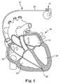
図1は、患者の身体内に埋め込まれたリードを有する例証的な医療デバイス12の略図である。示す例証的な実施形態では、医療デバイス12は、身体内に埋め込まれたパルス発生器を備える。医療デバイス12は、患者の心臓16内に挿入されたリード線14に結合される。心臓16は、右心房18、右心室20、左心房22、および左心室24を含む。パルス発生器12は、通常患者の胸部または腹部などの場所において、身体内の皮下に埋め込まれうるが、他の埋め込み場所が可能である。 FIG. 1 is a schematic illustration of an exemplary
リード線14の近位部分26は、パルス発生器12に結合されうる、または、パルス発生器と一体に形成されうる。次に、リード線14の遠位部分28は、図示するように、右心室20などの心臓16の所望の場所内に埋め込まれうる。例証的な実施形態は、患者の心臓16に挿入された単一リード線102だけを示すが、他の実施形態ではしかし、心臓16の他のエリアを電気刺激するために複数のリード線が利用されうる。一部の実施形態では、たとえば、第2のリード線の遠位部分(図示せず)は、右心房18に埋め込まれてもよい。さらにまたは代わりに、別のリードが、心臓16の左側を刺激するために、心臓16の左側に(たとえば、冠状静脈に)埋め込まれてもよい。心外膜リード線などの他のタイプのリードが、図1に示すリード線14に加えて、または、その代わりに利用されてもよい。 The
動作中、リード線14は、心臓16とパルス発生器12との間で電気信号を伝達するように構成されうる。たとえば、パルス発生器12がペースメーカである実施形態では、リード線14は、心臓16をペーシングするために電気治療刺激を送出するために利用されうる。パルス発生器12が埋め込み型心臓除細動器である実施形態では、リード線14は、心臓発作などの事象に応答して心臓16に電気ショックを送出するために利用されうる。一部の実施形態では、パルス発生器12は、ペーシング能力と除細動能力の両方を含む。 In operation, the
図2は、MRIスキャナによって生成されるRF電磁エネルギーに起因する、リード線14上で拾取されるRFエネルギーを表す、リード線14についての簡易等価回路30を示す略図である。図2に示すように、回路30内のVi34は、MRIスキャナからのリード線14によって拾取される等価エネルギー源を表す。 FIG. 2 is a schematic diagram illustrating a simplified
磁気共鳴撮像中、リード線14の長さは、アンテナと同様に機能し、MRIスキャナから身体に送信されるRFエネルギーを受信する。図2の電圧34は、たとえば、RFエネルギーからの、リード線14によって受信される結果として得られる電圧を表してもよい。リード線14によって拾取されるRFエネルギーは、たとえば、導電性組織内で回転磁場ベクトルに垂直な平面内で電場を発生するMRIスキャナによって生成される回転RF磁場に起因する可能性がある。リード線14の長さに沿うこれらの電場の接線方向成分は、リード線14に結合する。そのため、電圧Vi34は、リード線14の長さに沿う接線方向電場の積分(すなわち、電場の線積分)に等しい。 During magnetic resonance imaging, the length of the lead 14 functions like an antenna and receives RF energy transmitted from the MRI scanner to the body. The
回路30内のZlパラメータ32は、MRIスキャナのRF周波数においてリード線14が示す等価インピーダンスを表す。インピーダンス値Zl32は、たとえば、1.5テスラMRIスキャナの場合、64MHzのRF周波数において、または、3テスラMRIスキャナの場合、128MHzのRF周波数において、リード線14が示す、平行インダクタンスとコイルの巻回部ごとのキャパシタンス(turn by turn capacitance)に起因するインダクタンスまたは等価インピーダンスを表してもよい。リード線14のインピーダンスZlは、実数部分(すなわち、抵抗)と虚数部分(すなわち、リアクタンス)を有する複素量である。
回路30内のZb38は、リード線接触点における身体組織のインピーダンスを表してもよい。Zc36は、次に、リード線14の長さに沿って周囲組織に対するリード線14の容量性結合を表してもよく、その容量性結合は、高周波電流(エネルギー)が、MRIスキャナのRF周波数において周囲組織内に漏洩する経路を提供する可能性がある。吸収されるエネルギー(ソースVi34によって表される)を最小にすることは、組織とのリード線接触点において身体組織に伝えられるエネルギーを低減する。
図2で示す回路および以下で述べる関連する方程式は、MRI環境におけるリード線加熱の概念を示すためのものである。誘導電圧(または電流)の波長が回路のサイズに近い周波数において、図2に示すような一括式の単純な合算(simple lumped sum)システムは、MRI環境におけるリード線14の挙動を正確にモデル化しない可能性がある。その結果、これらの状況では、回路の適切な数学的記述のために、分散モデルがマクスウェルの方程式と共に使用されるべきである。ある場合には、分散モデルの近似が、フィールドソルバまたはシミュレータを使用して生成されうる。 The circuit shown in FIG. 2 and related equations described below are intended to illustrate the concept of lead heating in an MRI environment. At frequencies where the induced voltage (or current) wavelength is close to the size of the circuit, a simple simple summed system as shown in FIG. 2 accurately models the behavior of the
図2でさらに見てわかるように、リード線14は、MRIスキャナのRF周波数において周囲組織内へのある量の漏洩36を有する。38でさらに示すように、心臓16内の周囲身体組織に対するリード線電極の接触点にもインピーダンスが存在する。身体組織に送出される結果として得られる電圧Vbは、以下の式:
Vb=ViZbe/(Zbe+Zl) (ここで、Zbe=ZbとZcとの並列インピーダンス)
によって関連付けられてもよい。As can be further seen in FIG. 2, lead 14 has a certain amount of
Vb = ViZbe / (Zbe + Zl) (where Zbe = parallel impedance of Zb and Zc)
May be associated with each other.
周囲組織に対して通常接触が行われるリード線14の先端(tip)の温度は、38において(すなわち、「Zb」において)消散される電力に部分的に関連しており、その電力は、次に、Vbの2乗に関連する。38にて消散される電力に起因する温度上昇を最小にするために、したがって、リード線のインピーダンスZl(32)も最大にしながら。Vi(34)およびZc(38)を最小にすることが望ましい。一部の実施形態では、リード線14のインピーダンスZl(32)は、MRIスキャナのRF周波数で増加する可能性があり、接触点38において周囲身体組織内に消散される電力を低減するのを補助する。 The temperature at the
一部の実施形態では、リード線14のインピーダンスは、リード線14にインダクタンスを付加することによって、および/または、適した構築技法によって増加しうる。たとえば、リード線14のインダクタンスは、導体コイルの径を増加させることによって、および/または、導体コイルのピッチを減少させることによって増加しうる。コイルピッチを減少させることは、コイルの連続する巻回部間のキャパシタンス(すなわち、コイルの巻回部ごとのキャパシタンス)の増加をもたらす可能性がある。(コイルの螺旋形状による)インダクタンスと巻回部ごとのキャパシタンスの並列結合は、共振回路を構成する。螺旋状に巻かれたリード線構成の場合、リード線の共振周波数がMRIのRF周波数を超える場合、螺旋コイルは、インダクタとして働く。インダクタの場合、コイルエリアの断面を増加させること、および/または、コイルピッチを減少させることは、インダクタンスを増加させ、結果として、リード線14のインピーダンスを増加させる。 In some embodiments, the impedance of
アンテナと同様に、リード線によるエネルギー拾取は、対象とする周波数の波長に対する共振長に関連する。たとえば、ダイポールアンテナの場合、アンテナ長が、波長の半分または波長の整数倍であるとき、同調された、または、共振状態にあると考えられる。共振長において、アンテナのエネルギー拾取が最大になる。同様に、また、一部の実施形態では、リード線14は、リード線14内での共振を防止し、したがって、電圧Viを最小にするために離調されうる。図1に示す例証的な実施形態の場合、たとえば、リード線14は、長さL=整数×λ/2の共振周波数を有するアンテナとして機能する。一部の実施形態では、波長に影響を及ぼすリード線14の長さおよび/またはリード線14の構成パラメータは、リード線14内での共振を回避するように選択されうる。 Similar to antennas, energy pick-up by leads is related to the resonance length for the wavelength of the frequency of interest. For example, in the case of a dipole antenna, it is considered tuned or in resonance when the antenna length is half the wavelength or an integral multiple of the wavelength. The antenna picks up the energy at the resonance length. Similarly, and in some embodiments, lead 14 can be detuned to prevent resonance in
一部の実施形態では、MRI誘導RFエネルギーの波長に対してリード線14の長さを離調することに加えて、リード線14によって拾取される電磁エネルギー量をさらに低減するために、シールディングもリード線14に付加されうる。たとえば、シールディングによって拾取されるエネルギーは、リード線14の長さに沿って患者の身体に結合される可能性があり、エネルギーがリード線先端に結合することを防止する。シールディングおよび/またはリード線の長さに沿う、シールディングによって遮られたエネルギーの移動は、シールディング構成用の抵抗性材料を使用して、抵抗損としてエネルギーを消散させることによって抑制されうる。 In some embodiments, in addition to detuning the length of the
図3は、図1のリード線14の一部分をさらに詳細に示す長手方向断面図である。図4は、次に、図3のライン4−4を横切るリード線14を示す横方向断面図である。図3〜4に示すように、リード線14は、内側導体コア40およびリード線14の長さの少なくとも一部分に沿って内側導体コア40を放射状に囲む外側抵抗性シールド42を含む。内側導体コア40は、リード線14の遠位部分28上に配置される1つまたは複数の電極(図示せず)にパルス発生器12からのエネルギーを供給する電気導管として機能してもよい。リード線14が徐脈リード線である実施形態では、たとえば、内側導体コア40は、患者の心臓16をペーシングするため、かつ/または、心臓16内で起こる電気活動を検知するために使用される1つまたは複数の電極に治療エネルギーを供給する電気導管として役立ってもよい。あるいは、リード線14が頻脈リード線である実施形態では、内側導体コア40は、リード線14の遠位部分28上に配置される1つまたは複数の電極コイルにショックエネルギーを供給する電気導管として役立ってもよい。図3〜4の実施形態では、単一の内側導体コア40が示されるが、他の実施形態では、複数の内側導体が、リード線14上に配置される複数のペーシング/センス電極に電気エネルギーを伝達するために設けられてもよい。 FIG. 3 is a longitudinal cross-sectional view showing a portion of the
図3〜4の例証的な実施形態では、リード線14は、リード線14の長さの全てまたは一部分に沿って外側抵抗性シールド42と共直線的に延在する内側導体コア40と実質的に同軸の構成を有する。他の実施形態では、内側導体コア40は、リード線14の長さの全てまたは一部分に沿って外側抵抗性シールド42の内部を通って延在する螺旋形状導体コア(または、複数の同じ放射状に巻き付けられた螺旋形状導体)を備えうる。 In the illustrative embodiment of FIGS. 3-4, the
外側抵抗性シールド42は、内側導体コア40を放射状に囲む抵抗性材料の層または被膜を備えうる。一実施形態では、たとえば、外側抵抗性シールド42は、内側導体コア40を放射状に囲む内側導体40(たとえば単一導体)と一体に形成される抵抗性ジャケットを備える。一部の実施形態では、リード線14は、さらに、周囲身体組織および血液から導体コア40を電気的に絶縁するために、抵抗性シールド42の周りに絶縁性材料の層または被膜を含んでもよい。導体と抵抗性シールドとの間に絶縁体の層または被膜が存在する本明細書で論じられるさらなる実施形態では、抵抗性シールド42の周りに配設される絶縁性材料の層または被膜は、省略されてもよい。ただし、導体の長さが十分に小さい場合に限る。 The outer
外側抵抗性シールド42は、リード線14と接触する身体組織の加熱をもたらしうる、リード線14の長さに沿って受信されるRF電磁エネルギーの消散を容易にするために、内側導体コア40と比較して比較的高い抵抗を有してもよい。一部の実施形態では、たとえば、外側抵抗性シールド42の抵抗と内側導体コア40の抵抗の比は、約2と10との間の範囲にあってよい。外側抵抗性シールド42の例示的な抵抗は、50cmという長さが長いリード線の場合、約1kΩであってよいが、他の値が可能である。 The outer
一部の実施形態では、外側抵抗性シールド42と内側導体コア40との抵抗の差は、少なくとも部分的に、使用される材料(複数可)のタイプ、これらの材料の誘電率、ならびに他の因子に依存しうる。いくつかの実施形態では、たとえば、内側導体コア40は、コア40に沿う電気信号の低エネルギー伝達を容易にするように構成された比較的低い抵抗材料を備え、一方、外側抵抗性シールド42は、磁気共鳴撮像中に、リード線14の長さに沿って、リード線14上で受信されるRF電磁エネルギーを消散するように構成された比較的高い抵抗材料を備える。外側抵抗性シールド42として使用するのに適する高抵抗材料は、たとえば、金属、導電性ポリマー、および/または複合材料を含みうる。1つの例示的な実施形態では、内側導体コア40は、約28%〜30%の銀を含有する銀充填MP35Nワイヤであり、一方、外側抵抗性シールド42は、異なる、より抵抗性が高い材料の層または被膜(たとえば、管状ジャケット)を備える。外側抵抗性シールド42として使用するのに適する例示的な導電性ポリマーは、ポリフェニレンビニレンまたはポリフルオレンである。 In some embodiments, the resistance difference between the outer
高導電率シールドは、一般に、内側導体のよりよいシールディングを提供し、また表皮深さが小さいため、薄いシールディングが使用されることを可能にするが、こうしたシールディングの高い導電率は、リード線の長さに沿ってより容易にRFエネルギーを伝える可能性がある。そのため、たとえRFエネルギーがシールドから内側導体に結合しなくても、シールド自体が、リード線の長さに沿ってリード線先端の電極に向かってRFエネルギーを伝える可能性がある。電極において、または、電極の近くで、エネルギーのこの高い集中は、(たとえば、組織に容量的に結合することによって)周囲組織を直接加熱するか、または、内側導体が露出し、組織に接触する場所で、元のリード線にエネルギーを結合する。 High conductivity shields generally provide better shielding of the inner conductor, and because of the low skin depth, allow thin shielding to be used, but the high conductivity of such shielding is RF energy can be more easily transmitted along the length of the lead. Thus, even if RF energy does not couple from the shield to the inner conductor, the shield itself can transmit RF energy along the length of the lead toward the lead tip electrode. This high concentration of energy at or near the electrode either directly heats the surrounding tissue (eg, by capacitively coupling to the tissue) or the inner conductor is exposed and contacts the tissue In place, couple energy to the original lead.
図5および6は、MRI磁場の存在下で図3〜4のリード線上で受信されるRF電磁エネルギーのエネルギー流路を示す、それぞれ、長手方向断面図および横方向断面図である。図5および6に示すように、磁気共鳴撮像中に患者の身体内に送信されるRFエネルギーは、アンテナとして働くリード線14の長さに沿って受信される。交流電流が、導体の表面における、または、表面の近くの伝導に制限される、伝導性ワイヤの「表皮効果(skin effect)」特性のために、抵抗は、リード線の中心に向かって増加する。中心に向かうシールドの抵抗の増加はまた、一部の実施形態では、シールディングの周りに絶縁性材料を設けることによって増大する可能性がある。参照矢印46によって全体が示されるように、エネルギーがリード線14の長さに沿って移動するにつれて、エネルギーの大きさは、(消散のために)減少し、消散エネルギーは、リード線14の長さに沿って熱に変換される。これは、一般に、図5における左から右への矢印46のベクトル長の減少によって見られうる。図6にさらに見られるように、エネルギー46は、表皮効果のため、内側導体40に結合するのではなく、抵抗性シールド42の最小インピーダンス経路をとる。RFエネルギーが、電極/身体組織界面においてではなく、リード線14の長さに沿って消散するため、RFエネルギーからのリード線14によって吸収される熱は、リード線14の長さに沿って減衰する。 5 and 6 are longitudinal and transverse cross-sectional views, respectively, showing the energy flow path of RF electromagnetic energy received on the leads of FIGS. 3-4 in the presence of an MRI magnetic field. As shown in FIGS. 5 and 6, RF energy transmitted into the patient's body during magnetic resonance imaging is received along the length of the
図7は、抵抗性シールドの周りに放射状に配設された低熱インピーダンス絶縁体を有する別の例証的な実施形態によるリード線48を示す横方向断面図である。リード線48は、図3〜4に関して述べたリード線14と同様であり、リード線48上の1つまたは複数の電極にエネルギーを供給する電気導管として使用されうる内側導体コア50、および、リード線48の長さに沿ってRF電磁エネルギーを消散させるための、内側導体コア50の抵抗と比較して比較的高い抵抗を有する外側抵抗性シールド52を含む。 FIG. 7 is a transverse cross-sectional view illustrating a lead 48 according to another illustrative embodiment having low thermal impedance insulators disposed radially around a resistive shield.
図7の実施形態では、リード線48は、さらに、リード線48の長さに沿って生成される熱をリード線/組織界面に伝えるようになっている低熱インピーダンス絶縁体を含む。一部の実施形態では、絶縁体54は、外側抵抗性シールド52の周りに放射状に配設された絶縁性材料の層または被覆を備える。いくつかの実施形態では、たとえば、絶縁体54は、シリコーンまたはポリウレタンの薄い層または被膜であるが、他の構成が可能である。他の実施形態では、絶縁体54は、外側抵抗性シールド52の周りに放射状に配設された金属の薄い層または被覆である。一部の実施形態では、金属絶縁体54の厚さは、約10μmと約10,000μmとの間の範囲内にあるが、他の構成が可能である。 In the embodiment of FIG. 7, lead 48 further includes a low thermal impedance insulator adapted to conduct heat generated along the length of
一部の実施形態では、絶縁体54のために使用される材料は、約6と100との間の範囲内の比較的高い誘電率を有する。一部の実施形態では、絶縁体材料についての比較的高い誘電率は、炭素粒子、窒化ホウ素粒子、アルミニウム酸化物粒子などを絶縁体材料に添加することによって達成されうる。絶縁体54は、リード線48の長さに沿って一定である、リード線48の幅(または横方向断面)に沿って一定である、または、両方の組合せである誘電率の勾配を有しうる。磁気共鳴撮像中、その厚さ、誘電率、または両方の組合せを含む絶縁体54の特性は、電磁エネルギーおよび/または抵抗性シールド52によって生成された熱を、リード線48の長さに沿って周囲身体組織に伝える手段を提供しうる。 In some embodiments, the material used for
図8は、その幅にわたって抵抗の徐々の変化を有する別の例証的な実施形態によるリード線56を示す横方向断面図である。図8の実施形態では、リード線56は、その幅にわたって可変抵抗率を有する単一導体58を含む。参照矢印60によって全体が示されるように、導体58の抵抗率は、リード線56が周囲身体組織に接触するリード線56の外側表面62において抵抗率が最大になるように、その幅にわたって変化しうる。一部の実施形態では、リード線56の抵抗率は、導体58の中心部分64から外側表面62まで連続的に増加している。他の実施形態では、抵抗率は、リード線56の幅にわたる1つまたは複数の有限の場所で増加してもよい。 FIG. 8 is a transverse cross-sectional view illustrating a lead 56 according to another illustrative embodiment having a gradual change in resistance across its width. In the embodiment of FIG. 8, lead 56 includes a
MRIスキャン中、リード線56の外側表面62に向かって増加した抵抗率は、MRIデバイスから受信されたRFエネルギーを、リード線56の長さに沿う外側表面62においてまたは外側表面62の近くで消散させるのに役立ち、したがって、リード線56の内部に伝達されるエネルギー量を最小にする。外側表面62におけるまたは外側表面62の近くでのRFエネルギーのこの減衰は、交流電流が、内部導体58を通して、リード線先端に配置された電極に伝達されることを防止する。 During the MRI scan, the increased resistivity toward the
図9は、それぞれが異なる抵抗率を持つ複数の導体層を有する別の例証的な実施形態によるリード線66を示す横方向断面図である。図9に示すように、リード線66は、いくつかの抵抗が比較的高い外側導体70、72、74によって放射状に囲まれた内側導体68を含む。外側導体70、72、74はそれぞれ、リード線66の抵抗がその幅にわたって変化するように異なる抵抗率を有しうる。一部の実施形態では、また、参照矢印76によって全体が示されるように、外側導体層70、72、74のそれぞれの抵抗率は、リード線66の外側表面78においてまたは外側表面78の近くで抵抗率が最大になるようにリード線66の幅にわたって連続的に増加していてもよい。いくつかの実施形態では、たとえば、第1の外側導体層70は第1の抵抗率を有してもよく、第2の外側導体層72は、第1の抵抗率より大きい第2の抵抗率を有してもよく、第3の外側導体層74は、第1および第2の抵抗率より大きい第3の抵抗率を有してもよい。しかし、導体層の数および配置構成は異なってもよい。たとえば、3つの外側導体層70、72、74が図9に示されるが、他の実施形態では、それぞれが外側表面78に向かって連続的により大きな抵抗率を有する、より多いまたはより少ない数の外側導体層が、MRIスキャン中にリード線66上で受信されるRFエネルギーを消散させるために設けられてもよい。 FIG. 9 is a transverse cross-sectional view illustrating a lead 66 according to another illustrative embodiment having a plurality of conductor layers each having a different resistivity. As shown in FIG. 9, the
図8および9は、リード線抵抗率が、連続的に、または、リード線56、66の幅にわたる1つまたは複数の限定された場所において変化する実施形態を示すが、インピーダンスが、リード線56、66の長さの全てまたは一部分に沿って変化する他の実施形態も可能である。一部の実施形態では、たとえば、リード線56、66のインピーダンスは、リード線の遠位部分が、リード線の近位部分に比べて大きなインピーダンスを有するように、リード線56、66の長さに沿って増加する。リード線の長さに沿うインピーダンスの変化は、特定の特性(たとえば、高い誘電率、抵抗率など)を有する材料の選択によって、リード線の構造(たとえば、インダクタンス)によって、リード線の次元(たとえば、リード線の表面積)によって、ならびに、他の因子によって達成されうる。リード線長に沿ってリード線のインピーダンスを変化させることによって、リード線の長さに沿ってインピーダンス不連続点を生成することは、MRIスキャン中のリード線のエネルギー拾取に影響を及ぼす。一部の実施形態では、リード線の長さに沿って定在波が生成されることを防止するために、これらの不連続点は、リード線の長さに沿って分散されることができ、したがって、リード線電極における組織加熱が最小になる。 8 and 9 illustrate embodiments in which the lead resistivity varies continuously or in one or more limited locations across the width of the
図10は、抵抗性シールドと内側導体との間に絶縁体を有する別の例証的な実施形態によるリード線80を示す長手方向断面図である。図11は、次に、図10のライン11−11を横切るリード線80を示す横方向断面図である。リード線80は、図3〜4に関して述べたリード線14と同様であり、リード線80上の1つまたは複数の電極にエネルギーを供給する電気導管として使用されうる内側導体コア82、および、リード線80の長さに沿ってRFエネルギーを消散させるための、内側導体コア82の抵抗と比較して比較的高い抵抗を有する外側抵抗性シールド84を含む。 FIG. 10 is a longitudinal cross-sectional view illustrating a lead 80 according to another illustrative embodiment having an insulator between the resistive shield and the inner conductor. FIG. 11 is a lateral cross-sectional view showing a
図10〜11の実施形態では、リード線80は、さらに、外側抵抗性シールド84と内側導体コア82との間に配設された絶縁物層86を含む。絶縁物層86は、外側抵抗性シールド84上で受信されるRFエネルギーから内側導体コア82を電気的に絶縁するように構成される。内側導体コア82を電気的に絶縁するのに適する絶縁物層86の例は、約10ミル(mil)以下の薄層である。別の絶縁物層または被膜が、抵抗性シールド84の周りに配置される場合、使用される絶縁物層86は、薄くてもよく、一部の実施形態では、約1ミル厚以下であってよい。いくつかの実施形態では、内側コイル導体82、抵抗性シールド84、および絶縁物86を含むリード線80の外径は約50〜100ミルである。 In the embodiment of FIGS. 10-11, the
種々の実施形態では、抵抗性シールド付きワイヤは、コイル状導体を作るために巻き付けられることができ、インダクタンスを増加させることによってリード線にさらなるインピーダンスが付加される。図3の実施形態では、たとえば、導体40および抵抗性シールド42は、たとえば図18に関して本明細書でさらに論じる例証的なリード線118と同様に、螺旋状に巻かれることができ、したがって、導体40にインダクタンスが付加される。一部の実施形態では、コイル構造のために使用される抵抗性シールド付きワイヤは、比較的薄くてもよい(たとえば、10ミル未満)。一部の実施形態では、埋め込み部位においてコイル導体が組織および血液に接触することを防止するために、コイル状導体は、絶縁物チュービングまたはシーシング(たとえば、10ミルの絶縁性チュービング)内に挿入されうる。導体を形成するワイヤがそれぞれ、絶縁物層を有する場合、コイル導体の周りに配置された絶縁物チュービングまたはシーシングは、一般に非常に薄い(たとえば、せいぜい約1ミル)。 In various embodiments, the resistively shielded wire can be wound to make a coiled conductor, adding additional impedance to the lead by increasing the inductance. In the embodiment of FIG. 3, for example,
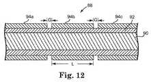
図12は、リード線の長さに沿って互いから離間しかつ電気的に絶縁された、いくつかの抵抗性シールドを有する別の例証的な実施形態によるリード線88を示す長手方向断面図である。図12に示すように、リード線88は、図10で示したリード線と同様であり、リード線88上の1つまたは複数の電極にエネルギーを供給する電気導管として使用されうる内側導体コア90、および、内側導体コア90を放射状に囲む絶縁物層92を含む。 FIG. 12 is a longitudinal cross-sectional view illustrating a lead 88 according to another illustrative embodiment having several resistive shields spaced apart and electrically isolated from each other along the length of the lead. is there. As shown in FIG. 12, the
図12の実施形態では、リード線88は、さらに、絶縁物層92および内側導体コア90の周りに放射状に配設された、いくつかの外側抵抗性シールド94a、94b、94cを含む。外側抵抗性シールド94a、94b、94cはそれぞれ、内側導体コア90の抵抗と比較して比較的大きい抵抗を有する材料の層または被膜を備えうる。一部の実施形態では、たとえば、外側抵抗性シールド94a、94b、94cの1つシールドの内側導体コア90に対する抵抗の比は、約2と10との間の範囲内にありうる。 In the embodiment of FIG. 12, lead 88 further includes a number of outer
外側抵抗性シールド94a、94b、94cはそれぞれ、図示するように、リード線88の長さの一部分に沿って延在し、いくつかの小さなギャップGを介して互いから分離される。長手方向に隣接する各シールド94a、94b、94c間のギャップGは、各シールド94a、94b、94cが他のシールド94a、94b、94cから電気的に絶縁されるのに十分である。一部の実施形態では、たとえば、外側抵抗性シールド94a、94b、94cは、約4mm〜5mmのギャップGによって互いから分離されうる。他の実施形態では、外側抵抗性シールド94a、94b、94cのそれぞれを分離するギャップGは、シールド94a、94b、94cの電気特性(たとえば、シールド94a、94b、94cの材料および厚さ)、リード線88上で受信されるRFエネルギー量、ならびに他の因子に応じてより大きくてもよく、または、より小さくてもよい。 Each of the outer
抵抗性シールド94a、94b、94cのそれぞれの長さLは、シールド94a、94b、94cのセクションを離調し、MRIデバイスによって提供されるRFエネルギーの周波数に基づく共振を防止するように選択されうる。一部の実施形態では、たとえば、外側抵抗性シールド94a、94b、94cはそれぞれ、リード線88上で受信されるRFエネルギーの波長の1/4以下の長さLを有し、したがって、シールド94a、94b、94cのそれぞれは離調される。使用時、拾取されるエネルギーは、各シールド94a、94b、94cの端部の近くに集中するのではなく、リード線の長さに沿って均等に分散される(抵抗性材料内で均等に消散される)ことができ、次に、隣接するシールド94a、94b、94cに容量的に結合し、リード線先端に移動する。ギャップGはまた、拾取されるエネルギーが、リード線の端部に移動し、リード線電極が周囲身体組織に接触する場所で消散する(この場所での身体組織の温度上昇をもたらしうる)ことを防止するのに役立つ。 The length L of each of the
図13は、MRI磁場の存在下でリード線88によって受信されるRF電磁エネルギーのエネルギー流路を示す、図12のリード線88の別の長手方向断面図である。図13に示すように、MRIスキャン中に患者の身体内に送信されるRFエネルギーは、外側抵抗性シールド94a、94b、94cのそれぞれの上で受信される。シールド94a、94b、94cの抵抗が比較的高いため、また、参照矢印98で全体が示されるように、RFエネルギーは、各シールド94a、94b、94cの長さLだけに沿って、リード線88の表面において、または、表面の近くで消散される。シールド94a、94b、94cのそれぞれの間の小さなギャップGは、シールドのうちの1つのシールド(たとえば、シールド94b)上に誘導されるRFエネルギーが隣接するシールド(たとえば、シールド94c)に送信されることを防止する。結果として、リード線88上の1つのセクション上のRFエネルギーの流れが、遮断され、リード線88の全長に沿ってリード線先端に送信されることが防止される。したがって、遮断されたRFエネルギーは、インピーダンスの不整合のために、反射され、最終的に、抵抗性シールド94a、94b、94c内で消散される。 FIG. 13 is another longitudinal cross-sectional view of
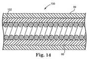
図14は、抵抗性シールドによって放射状に囲まれた螺旋形状内側導体コイルを有する別の例証的な実施形態によるリード線100を示す長手方向断面図である。図14に示すように、リード線100は、図10〜11に関して述べたリード線80と同様であり、図面において同じように表示された同じ要素を有する。しかし、図14の実施形態では、内側導体102は、リード線100の内部を通って延在し、MRI RF周波数においてリード線100にインダクタンスを付加する螺旋形状導体コイルである。外側抵抗性シールド84と対照的に、導体コイル102は、リード線100上の電極に対して治療エネルギーの低エネルギー伝達を容易にするように構成された導電性の低抵抗材料から作製される。一部の実施形態では、たとえば、内側導体コイル102は、約28%〜30%の銀を含有する銀充填MP35Nワイヤから作製され、一方、外側抵抗性部材84は、異なるより抵抗性が高い材料を含む。 FIG. 14 is a longitudinal cross-sectional view illustrating a lead 100 according to another illustrative embodiment having a helically shaped inner conductor coil radially surrounded by a resistive shield. As shown in FIG. 14, lead 100 is similar to lead 80 described with respect to FIGS. 10-11 and has the same elements displayed in the same way in the drawings. However, in the embodiment of FIG. 14, the
図14の実施形態では、外側抵抗性シールド84は、リード線100の長さの全てまたは一部分に沿って連続してかつ遮断されずに延在してもよい。図15に示す別の例証的なリード線104では、リード線104は、図示するように、それぞれが、いくつかの小さなギャップGを介してリード線104の長さに沿って互いから離間しかつ電気的に絶縁される、いくつかの外側抵抗性シールド106a、106b、106cを含む。外側抵抗性シールド106a、106b、106cのそれぞれの長さLは、リード線104を離調し、MRIデバイスによって提供されるRFエネルギーの周波数に基づく共振を防止するように選択されうる。一部の実施形態では、たとえば、外側抵抗性シールド106a、106b、106cはそれぞれ、リード線104上で受信されるRFエネルギーの波長の1/4以下の長さLを有する。 In the embodiment of FIG. 14, the outer
図16は、螺旋形状抵抗性コイルによって放射状に囲まれた螺旋形状内側導体コイルを有する別の例証的な実施形態によるリード線106を示す長手方向断面図である。リード線106は、図14に関して述べたリード線100と同様であり、リード線106上の1つまたは複数の電極にエネルギーを供給する電気導管として使用されうる螺旋形状内側導体コイル108、内側導体コイル108を放射状に囲む絶縁物層110、および、吸収されたRFエネルギーをリード線106の長さに沿って消散させるための、内側導体コイル108の抵抗と比較して比較的高い抵抗を有する外側抵抗性シールド112を含む。一部の実施形態では、内側導体コイル108は、単一フィラーワイヤコイルである。他の実施形態では、内側導体コイル108は、マルチフィラーワイヤコイルである。 FIG. 16 is a longitudinal cross-sectional view illustrating a lead 106 according to another illustrative embodiment having a helical inner conductor coil radially surrounded by a helical resistive coil. The
図16の実施形態では、外側抵抗性シールド112は、内側導体コイル108および絶縁物層110を放射状に囲む螺旋形状抵抗性コイルを備える。抵抗性コイル112は、リード線106の長さに沿う周囲身体組織内への、リード線106上で受信されるRFエネルギーの消散を容易にするために、内側導体コイル108の抵抗と比較して比較的高い抵抗を有する。一部の実施形態では、たとえば、抵抗性コイル112の抵抗の内側導体コイル108の抵抗に対する比は、約2と10との間の範囲にあってよい。一実施形態では、内側導体コイル108は、約28%〜30%の銀を含有する銀充填MP35Nワイヤから作製され、一方、外側抵抗性部材84は、純粋のMP35Nなどの異なるより抵抗性が高い材料を含む。 In the embodiment of FIG. 16, the outer
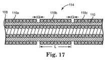
図16の実施形態では、抵抗性コイル112は、リード線106の長さの全てまたは一部分に沿って連続してかつ遮断されずに延在してもよい。図17に示す別の例証的なリード線114では、リード線114は、図示するように、それぞれが、いくつかの小さなギャップGを介してリード線114の長さに沿って互いから離間しかつ電気的に絶縁される、いくつかの抵抗性コイル116a、116b、116cを含む。抵抗性コイル116a、116b、116cのそれぞれの長さLは、リード線114を離調し、MRIデバイスによって送信されるRFエネルギーの周波数に基づく共振を防止するように選択されうる。一部の実施形態では、たとえば、抵抗性コイル116a、116b、116cはそれぞれ、リード線114によって受信されるRFエネルギーの波長の1/4以下の長さLを有する。 In the embodiment of FIG. 16, the
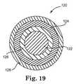
図18は、別の例証的な実施形態によるリード線118を示す長手方向断面図である。図18に示すように、リード線118は、リード線118の長さの少なくとも一部分に沿って延在する螺旋状導体コイル120を含む。導体コイル120は、リード線118上の1つまたは複数の電極にエネルギーを供給する電気導管として構成される。いくつかの実施形態では、導体コイル120は、リード線118の長さに沿って導体コイル120を放射状に拘束するのに役立つ外側部材121内に入れられる。一部の実施形態では、たとえば、外側部材121は、導体コイル120の周りに放射状に配設されたシリコーンまたはポリウレタンのジャケットを備える。 FIG. 18 is a longitudinal cross-sectional view illustrating a lead 118 according to another illustrative embodiment. As shown in FIG. 18, lead 118 includes a
図19は、図18の螺旋導体コイル120の構成をさらに詳細に示す長手方向断面図である。図19にさらに示すように、導体コイル120は、内側導体コア122および内側コア122の周りに放射状に配設された外側抵抗性シールド124を含む。抵抗性シールド124は、(たとえば、共押出しプロセスによって)内側導体コア122と一体に形成され、導体コア122の抵抗より大きい抵抗を有する材料を備える。一部の実施形態では、たとえば、抵抗性シールド124の抵抗と導体コア122の抵抗の比は、約2と10との間の範囲にありうる。 FIG. 19 is a longitudinal sectional view showing the configuration of the
図18〜19の実施形態では、導体コイル120は、さらに、内側導体コア122と外側抵抗性シールド124との間に配設された絶縁物126の層または被膜を含む。一部の実施形態では、絶縁物128の第2の層または被膜はまた、シールド124をさらに絶縁するために、外側抵抗性シールド124を覆って設けられてもよい。 In the embodiment of FIGS. 18-19, the
いくつかの実施形態では、また、図20にさらに示すように、内側導体コア122と外側抵抗性シールド124との間の絶縁物126の第1の層または被膜がなくされうる。たとえば抵抗性シールド124の表皮深さが十分に大きい(たとえば、4より大きい)場合、シールド124と内側導体コア122との間の界面における電流密度の減衰のため、RFエネルギーによって生成される交流電流が、シールド124の深さを十分に貫通できないため、絶縁物126の第1の層または被膜がなくされてもよい。 In some embodiments, and as further shown in FIG. 20, the first layer or coating of
導体がコイル状である実施形態では、コイル導体の外径およびピッチを含むコイル導体の幾何形状は、リード線の長さに沿うエネルギーの移動を抑制するために、リード線のインダクタンス、したがって、インピーダンスを増加させるように構成されうる。一部の実施形態では、たとえば、コイル導体のインダクタンスは、コイル巻回数を増加させることによって(たとえば、コイル導体のピッチを減少させることによって)、コイル導体の外径を増加させることによって、または、両方の組合せによって増加されうる。コイル導体のインピーダンスが部分的にそのインダクタンスに基づくため、コイル巻回数を増加させる、かつ/または、導体の外径を増加させることによってコイル導体のインダクタンスを増加させることは、導体の総合インピーダンスの増加をもたらす。MRI適用時のRF周波数(たとえば、64MHz)におけるリード線の総合インピーダンスが、部分的にリード線のインダクタンスの関数であるため、コイル導体インダクタンスのこの増加は、リード線の長さに沿ってリード線電極に向かうリード線による吸収RFエネルギーの移動の減少をもたらす。 In embodiments where the conductor is coiled, the geometry of the coil conductor, including the outer diameter and pitch of the coil conductor, reduces the inductance of the lead, and thus the impedance, to suppress energy transfer along the length of the lead. May be configured to increase. In some embodiments, for example, the inductance of the coil conductor is increased by increasing the number of coil turns (eg, by decreasing the pitch of the coil conductor), by increasing the outer diameter of the coil conductor, or It can be increased by a combination of both. Since the impedance of the coil conductor is based in part on its inductance, increasing the coil conductor inductance by increasing the number of coil turns and / or increasing the outer diameter of the conductor will increase the overall impedance of the conductor. Bring. Since the total impedance of the lead at RF frequencies (eg, 64 MHz) during MRI application is partially a function of lead inductance, this increase in coil conductor inductance is along the length of the lead. This results in a decrease in the transfer of absorbed RF energy by the lead towards the electrode.
一部の実施形態では、コイル導体は、約0.005インチの幅および約0.016インチと約0.066インチとの間の範囲内のコイル径(すなわち、外径)を有する螺旋形状ワイヤコイル導体を備えうる。いくつかの実施形態では、たとえば、コイル導体は、少なくとも0.036インチ、0.050インチ、0.060インチ、または0.066インチのコイル径を有しうる。しかし、他のコイル径構成が可能である。 In some embodiments, the coil conductor is a helical wire having a width of about 0.005 inches and a coil diameter (ie, outer diameter) in the range between about 0.016 inches and about 0.066 inches. A coil conductor may be provided. In some embodiments, for example, the coil conductor may have a coil diameter of at least 0.036 inches, 0.050 inches, 0.060 inches, or 0.066 inches. However, other coil diameter configurations are possible.
コイル導体のピッチはまた、リード線のインダクタンス、したがって、インピーダンスを増加させるように構成されうる。一部の実施形態では、導体のピッチは、0.005インチと0.160インチとの間の範囲内でありうる。しかし、他のコイルピッチ構成が可能である。一般に、コイルピッチが増加するにつれて、リード線電極における加熱もまた増加する。0.035インチ外径コイルの場合、また、一部の実施形態では、導体のピッチは、わずか約0.008インチ、より具体的には約0.005インチであるべきである。しかし、より大きな外径コイルの場合、最小ピッチは、より大きく、一部の実施形態では、約0.025インチまでで、かつ、約0.025インチを含む。 The pitch of the coil conductors can also be configured to increase the lead inductance, and thus the impedance. In some embodiments, the conductor pitch may be in the range between 0.005 inches and 0.160 inches. However, other coil pitch configurations are possible. In general, as the coil pitch increases, the heating at the lead wire electrode also increases. For a 0.035 inch outer diameter coil, and in some embodiments, the conductor pitch should be only about 0.008 inches, more specifically about 0.005 inches. However, for larger outer diameter coils, the minimum pitch is larger, in some embodiments up to about 0.025 inches and including about 0.025 inches.
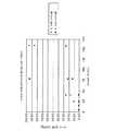
コイルピッチが増加し、コイル径が減少するため、コイル導体のコイルピッチとコイル径との間に強い相互依存性が存在する。図21は、螺旋形状ワイヤコイル導体によって遠位リード線先端に伝えられる吸収RFエネルギーの量に対するコイルピッチとコイル径の相互依存性を示すチャートである。図21は、たとえば、各導体が約50cmの長さを有し、MP35N材料を含む、0.036インチコイル径ワイヤ導体および0.066インチコイル径ワイヤ導体について、コイルピッチとコイル径の関数としてのピーク比吸収率(specific absorption rate)(SAR)を示してもよい。導体のそれぞれのコイルピッチが増加するにつれて、導体によって吸収されるRFエネルギーの量を表すピークSARは、2次関数として増加する。図21に示すように、0.036インチワイヤコイルについて約0.020インチ(20ミル)より大きいコイルピッチ、および、0.066インチワイヤコイルについて約0.050インチ(50ミル)より大きいコイルピッチは、リード線電極において身体組織の温度を増加させうるピークSARのかなりの上昇をもたらす。図21にさらに示すように、同等のコイルピッチ値において、より大きなコイル径の導体についてのピークSARは、一般に、より小さいコイル径の導体についてのピークSARより小さい。 Since the coil pitch increases and the coil diameter decreases, there is a strong interdependence between the coil pitch and the coil diameter of the coil conductor. FIG. 21 is a chart showing the interdependence of coil pitch and coil diameter on the amount of absorbed RF energy delivered to the distal lead tip by the helical wire coil conductor. FIG. 21 shows, for example, as a function of coil pitch and coil diameter for 0.036 inch coil diameter wire conductors and 0.066 inch coil diameter wire conductors, each conductor having a length of approximately 50 cm and comprising MP35N material. The specific absorption rate (SAR) may be indicated. As the respective coil pitch of the conductors increases, the peak SAR representing the amount of RF energy absorbed by the conductors increases as a quadratic function. As shown in FIG. 21, a coil pitch greater than about 0.020 inch (20 mils) for a 0.036 inch wire coil and a coil pitch greater than about 0.050 inch (50 mils) for a 0.066 inch wire coil. Results in a significant increase in peak SAR that can increase body tissue temperature at the lead electrode. As further shown in FIG. 21, at equivalent coil pitch values, the peak SAR for a larger coil diameter conductor is generally less than the peak SAR for a smaller coil diameter conductor.
リード線の他の設計パラメータはまた、リード線によるリード線加熱を低減するために選択されうる。一部の実施形態では、たとえば、コイル導体の周りに設けられる絶縁物は、リード線加熱を低減するように選択されうる。絶縁物の厚さは、リード線の長さに沿ってどれだけのエネルギーが周囲身体組織の内部にまたは周囲身体組織の外部に結合するかを変える。ある場合には、比較的薄い絶縁物または高い誘電率を有する絶縁物は、身体組織との接触点におけるリード線の温度上昇を最小にしうる。コイル状ワイヤ導体についての比較的薄い絶縁物の例は、約0.015インチ未満の壁厚を有するが、他の絶縁物の厚さが可能である。 Other design parameters for the lead can also be selected to reduce lead heating by the lead. In some embodiments, for example, an insulator provided around the coil conductor can be selected to reduce lead heating. The thickness of the insulator changes how much energy is coupled into or out of the surrounding body tissue along the length of the lead. In some cases, a relatively thin insulator or an insulator with a high dielectric constant may minimize the temperature rise of the lead at the point of contact with body tissue. An example of a relatively thin insulator for a coiled wire conductor has a wall thickness of less than about 0.015 inches, although other insulator thicknesses are possible.
種々の変更および追加が、本発明の範囲から逸脱することなく、論じられた例示的な実施形態に対して行われうる。たとえば、上述した実施形態は特定の特徴を参照するが、本発明の範囲はまた、特徴の異なる組合せを有する実施形態および述べた特徴の全てを含まない実施形態を含む。したがって、本発明の範囲は、特許請求項の全ての均等物と共に、特許請求項の範囲内に入る全てのこうした代替物、変更物、および変形物を包含することを意図される。 Various changes and additions can be made to the exemplary embodiments discussed without departing from the scope of the present invention. For example, while the embodiments described above refer to particular features, the scope of the invention also includes embodiments having different combinations of features and embodiments that do not include all of the described features. Accordingly, the scope of the present invention is intended to embrace all such alternatives, modifications and variations that fall within the scope of the claims, along with all equivalents of the claims.
Claims (14)
Translated fromJapaneseリード線を備え、前記リード線は、電極に動作可能に結合された内側電気導体と、複数の外側抵抗性シールドとを含み、前記複数の外側抵抗性シールドの各々は、前記リード線の長さの少なくとも一部分に沿って前記内側電気導体の周りに放射状に配設された螺旋形状コイルを含み、前記螺旋形状コイルは、非導電性ギャップにより互いから離間し、かつ電気的に絶縁されており、
前記内側電気導体は第1の抵抗を有し、
前記螺旋形状コイルは、各々前記第1の抵抗より大きい第2の抵抗を有し、
前記螺旋形状コイルは、MRIデバイスによって受信されるRF電磁エネルギーを前記リード線の長さに沿って消散させるように構成されている、医療デバイス。An implantable medical device for use in a magnetic resonance imaging environment,
A lead wire, the lead wire including an inner electrical conductor operably coupled to the electrodeand a plurality of outer resistive shields, each of the plurality of outer resistive shields having a length of the lead wire. Aspiral coil disposed radially about the inner electrical conductor along at least a portion of thecoil , thespiral coil being spaced apart from each other by a non-conductive gap and electrically insulated;
The inner electrical conductor has a first resistance;
Thehelical coilseach have a second resistance greater than the first resistance;
The medical device, wherein thehelical coil is configured to dissipate RF electromagnetic energy received by an MRI device along the length of the lead.
リード線を備え、前記リード線は、電極に動作可能に結合された螺旋形状電気導体コイル、および複数の抵抗性シールドを含み、該複数の抵抗性シールドの各々は前記リード線の長さに沿って前記導体コイルの一部分を放射状に囲んでおり、
前記導体コイルは、導電性材料を含み、第1の抵抗を有し、
外側抵抗性シールドの各々は、前記リード線の長さに沿って、互いから、及び前記導体コイルから離間し、かつ電気的に絶縁され、前記外側抵抗性シールドの各々は、前記導体コイルの前記第1の抵抗より大きい第2の抵抗を有し、
少なくとも1つの外側抵抗性シールドは、前記リード線の長さに沿ってMRIデバイスによって受信されるRF電磁エネルギーを消散させるように構成されている、医療デバイス。An implantable medical device for use in a magnetic resonance imaging environment,
A lead wire, the lead wire including a helically shaped electrical conductor coil operably coupled to an electrode and a plurality of resistive shields, each of the plurality of resistive shields extending along a length of the lead wire. A portion of the conductor coil is radially enclosed,
The conductor coil includes a conductive material and has a first resistance;
Each of the outer resistive shields is spaced from and electrically isolatedfrom each other and fromthe conductor coil along the length of the lead, and each of the outer resistive shields is Having a second resistance greater than the first resistance;
The medical device, wherein the at least one outer resistive shield is configured to dissipate RF electromagnetic energy received by the MRI device along the length of the lead.
リード線を備え、前記リード線は、電極に動作可能に結合された電気導体ワイヤを含み、前記電気導体ワイヤは、前記導体ワイヤの中心部分と前記導体ワイヤの外側部分との間で前記リード線の幅にわたって連続的に変化する抵抗率を有し、
前記導体ワイヤの中心部分は、第1の抵抗率を有し、
前記導体ワイヤの外側部分は、第1の抵抗率より大きい第2の抵抗率を有し、
前記導体ワイヤの外側部分は、前記リード線の長さに沿ってMRIデバイスによって受信されるRF電磁エネルギーを消散させるように構成されている、医療デバイス。An implantable medical device for use in a magnetic resonance imaging environment,
A lead wire, wherein the lead wire includes an electrical conductor wire operably coupled to an electrode, the electrical conductor wire between the central portion of the conductor wire and the outer portion of the conductor wire. Having a resistivitythat variescontinuously over the width of
A central portion of the conductor wire has a first resistivity;
The outer portion of the conductor wire has a second resistivity greater than the first resistivity;
The medical device, wherein the outer portion of the conductor wire is configured to dissipate RF electromagnetic energy received by the MRI device along the length of the lead.
Applications Claiming Priority (3)
| Application Number | Priority Date | Filing Date | Title |
|---|---|---|---|
| US12/329,257 | 2008-12-05 | ||
| US12/329,257US8275464B2 (en) | 2007-12-06 | 2008-12-05 | Leads with high surface resistance |
| PCT/US2008/087068WO2010065049A1 (en) | 2008-12-05 | 2008-12-17 | Leads with high surface resistance |
Publications (2)
| Publication Number | Publication Date |
|---|---|
| JP2012510854A JP2012510854A (en) | 2012-05-17 |
| JP5430671B2true JP5430671B2 (en) | 2014-03-05 |
Family
ID=40834422
Family Applications (1)
| Application Number | Title | Priority Date | Filing Date |
|---|---|---|---|
| JP2011539494AExpired - Fee RelatedJP5430671B2 (en) | 2008-12-05 | 2008-12-17 | Lead wire with high surface resistance |
Country Status (4)
| Country | Link |
|---|---|
| US (3) | US8275464B2 (en) |
| EP (1) | EP2355890B1 (en) |
| JP (1) | JP5430671B2 (en) |
| WO (1) | WO2010065049A1 (en) |
Families Citing this family (64)
| Publication number | Priority date | Publication date | Assignee | Title |
|---|---|---|---|---|
| US8509913B2 (en)* | 2001-04-13 | 2013-08-13 | Greatbatch Ltd. | Switched diverter circuits for minimizing heating of an implanted lead and/or providing EMI protection in a high power electromagnetic field environment |
| US8396568B2 (en)* | 2002-04-11 | 2013-03-12 | Medtronic, Inc. | Medical electrical lead body designs incorporating energy dissipating shunt |
| US7904178B2 (en)* | 2002-04-11 | 2011-03-08 | Medtronic, Inc. | Medical electrical lead body designs incorporating energy dissipating shunt |
| US7844344B2 (en) | 2004-03-30 | 2010-11-30 | Medtronic, Inc. | MRI-safe implantable lead |
| US7610101B2 (en) | 2006-11-30 | 2009-10-27 | Cardiac Pacemakers, Inc. | RF rejecting lead |
| US9044593B2 (en) | 2007-02-14 | 2015-06-02 | Medtronic, Inc. | Discontinuous conductive filler polymer-matrix composites for electromagnetic shielding |
| US8483842B2 (en) | 2007-04-25 | 2013-07-09 | Medtronic, Inc. | Lead or lead extension having a conductive body and conductive body contact |
| WO2009076169A2 (en)* | 2007-12-06 | 2009-06-18 | Cardiac Pacemakers, Inc. | Implantable lead with shielding |
| US8275464B2 (en)* | 2007-12-06 | 2012-09-25 | Cardiac Pacemakers, Inc. | Leads with high surface resistance |
| AU2008335462B2 (en) | 2007-12-06 | 2014-02-20 | Cardiac Pacemakers, Inc. | Implantable lead having a variable coil conductor pitch |
| WO2009100003A1 (en)* | 2008-02-06 | 2009-08-13 | Cardiac Pacemakers, Inc. | Lead with mri compatible design features |
| US8255055B2 (en)* | 2008-02-11 | 2012-08-28 | Cardiac Pacemakers, Inc. | MRI shielding in electrodes using AC pacing |
| US9037263B2 (en) | 2008-03-12 | 2015-05-19 | Medtronic, Inc. | System and method for implantable medical device lead shielding |
| WO2009134901A1 (en)* | 2008-04-30 | 2009-11-05 | Medtronic, Inc. | Magnetic resonance imaging shunt electrodes with self-healing coatings |
| US8103360B2 (en) | 2008-05-09 | 2012-01-24 | Foster Arthur J | Medical lead coil conductor with spacer element |
| CN102186532A (en)* | 2008-10-15 | 2011-09-14 | 皇家飞利浦电子股份有限公司 | Probe for implantable electro-stimulation device |
| US20100106215A1 (en)* | 2008-10-23 | 2010-04-29 | Stubbs Scott R | Systems and methods to detect implantable medical device configuaration changes affecting mri conditional safety |
| WO2010064962A1 (en)* | 2008-12-02 | 2010-06-10 | St. Jude Medical Ab | A medical implantable lead and a method for manufacturing the same |
| US8285396B2 (en)* | 2009-01-05 | 2012-10-09 | Kenergy, Inc. | MRI compatible electrical lead for an implanted electronic medical device |
| US9084883B2 (en) | 2009-03-12 | 2015-07-21 | Cardiac Pacemakers, Inc. | Thin profile conductor assembly for medical device leads |
| US10035014B2 (en)* | 2009-04-30 | 2018-07-31 | Medtronic, Inc. | Steering an implantable medical lead via a rotational coupling to a stylet |
| ES2547713T3 (en)* | 2009-06-26 | 2015-10-08 | Cardiac Pacemakers, Inc. | Bypass of a medical device that includes a single-coil coil with improved torque transmission capacity and reduced RM heating |
| US8335572B2 (en) | 2009-10-08 | 2012-12-18 | Cardiac Pacemakers, Inc. | Medical device lead including a flared conductive coil |
| WO2011043898A2 (en)* | 2009-10-09 | 2011-04-14 | Cardiac Pacemakers, Inc. | Mri compatible medical device lead including transmission line notch filters |
| US9254380B2 (en) | 2009-10-19 | 2016-02-09 | Cardiac Pacemakers, Inc. | MRI compatible tachycardia lead |
| US9014815B2 (en)* | 2009-11-19 | 2015-04-21 | Medtronic, Inc. | Electrode assembly in a medical electrical lead |
| US8406895B2 (en)* | 2009-12-30 | 2013-03-26 | Cardiac Pacemakers, Inc. | Implantable electrical lead including a cooling assembly to dissipate MRI induced electrode heat |
| US8306630B2 (en)* | 2009-12-30 | 2012-11-06 | Cardiac Pacemakers, Inc. | Apparatus to selectively increase medical device lead inner conductor inductance |
| US8494651B2 (en)* | 2009-12-30 | 2013-07-23 | Cardiac Pacemakers, Inc. | Implantable leads with a conductor coil having two or more sections |
| US9750944B2 (en) | 2009-12-30 | 2017-09-05 | Cardiac Pacemakers, Inc. | MRI-conditionally safe medical device lead |
| WO2011081713A1 (en) | 2009-12-31 | 2011-07-07 | Cardiac Pacemakers, Inc. | Mri conditionally safe lead with multi-layer conductor |
| US8391994B2 (en) | 2009-12-31 | 2013-03-05 | Cardiac Pacemakers, Inc. | MRI conditionally safe lead with low-profile multi-layer conductor for longitudinal expansion |
| WO2011103444A1 (en) | 2010-02-19 | 2011-08-25 | Cardiac Pacemakers, Inc. | Lead including conductors configured for reduced mri-induced currents |
| WO2011123005A1 (en)* | 2010-03-31 | 2011-10-06 | St. Jude Medical Ab | Medical implantable lead |
| US9126031B2 (en) | 2010-04-30 | 2015-09-08 | Medtronic, Inc. | Medical electrical lead with conductive sleeve head |
| US8583258B2 (en) | 2010-05-05 | 2013-11-12 | Biotronik Se & Co. Kg | Electrode lead in particular for use with a medical implant |
| US8825181B2 (en) | 2010-08-30 | 2014-09-02 | Cardiac Pacemakers, Inc. | Lead conductor with pitch and torque control for MRI conditionally safe use |
| US8630718B2 (en) | 2010-11-18 | 2014-01-14 | Cardiac Pacemakers, Inc. | Insulative structure for MRI compatible leads |
| US20120130462A1 (en)* | 2010-11-24 | 2012-05-24 | Biotronik Se & Co. Kg | Implantable Lead Comprising an Elongate Lead Body |
| US8862246B2 (en)* | 2010-12-17 | 2014-10-14 | Biotronik Se & Co. Kg | Implantable device |
| US8942825B2 (en) | 2010-12-17 | 2015-01-27 | Biotronik Se & Co. Kg | Implantable device with elongated electrical conductor |
| US8942826B2 (en) | 2010-12-17 | 2015-01-27 | Biotronik Se & Co. Kg | Implantable device with extended electrical conductor |
| EP2667930A2 (en)* | 2011-01-26 | 2013-12-04 | Boston Scientific Neuromodulation Corporation | Systems and methods for making and using electrical stimulation systems with improved rf compatibility |
| EP2497418A1 (en)* | 2011-03-10 | 2012-09-12 | Koninklijke Philips Electronics N.V. | Current protection for electrode-based monitoring systems |
| US8666512B2 (en) | 2011-11-04 | 2014-03-04 | Cardiac Pacemakers, Inc. | Implantable medical device lead including inner coil reverse-wound relative to shocking coil |
| CN103957979B (en) | 2011-11-29 | 2017-09-12 | 皇家飞利浦有限公司 | For the pipe being introduced into subject |
| US9463317B2 (en) | 2012-04-19 | 2016-10-11 | Medtronic, Inc. | Paired medical lead bodies with braided conductive shields having different physical parameter values |
| AU2013249088B2 (en) | 2012-04-20 | 2015-12-03 | Cardiac Pacemakers, Inc. | Implantable medical device lead including a unifilar coiled cable |
| JP2013232356A (en)* | 2012-04-27 | 2013-11-14 | Junkosha Co Ltd | Coiled cable |
| US8954168B2 (en) | 2012-06-01 | 2015-02-10 | Cardiac Pacemakers, Inc. | Implantable device lead including a distal electrode assembly with a coiled component |
| US8666511B2 (en) | 2012-07-30 | 2014-03-04 | Medtronic, Inc. | Magnetic resonance imaging compatible medical electrical lead and method of making the same |
| JP6069499B2 (en) | 2012-08-31 | 2017-02-01 | カーディアック ペースメイカーズ, インコーポレイテッド | Lead wire with low peak MRI heating |
| US8983623B2 (en) | 2012-10-18 | 2015-03-17 | Cardiac Pacemakers, Inc. | Inductive element for providing MRI compatibility in an implantable medical device lead |
| US9993638B2 (en) | 2013-12-14 | 2018-06-12 | Medtronic, Inc. | Devices, systems and methods to reduce coupling of a shield and a conductor within an implantable medical lead |
| WO2015123249A1 (en) | 2014-02-11 | 2015-08-20 | Cardiac Pacemakers, Inc | Rf shield for an implantable lead |
| WO2015130753A1 (en) | 2014-02-26 | 2015-09-03 | Cardiac Pacemakers, Inc | Construction of an mri-safe tachycardia lead |
| CN104083823B (en)* | 2014-06-27 | 2017-09-26 | 清华大学 | A kind of implanted electrode compatible MRI |
| EP3171931B1 (en) | 2014-07-23 | 2021-11-10 | Medtronic, Inc. | Methods of shielding implantable medical leads and implantable medical lead extensions |
| EP3191175B1 (en) | 2014-07-24 | 2022-03-02 | Medtronic, Inc. | Apparatus for shielding implantable medical leads and lead extensions |
| AU2015373537B2 (en)* | 2014-12-29 | 2020-09-03 | Smith & Nephew Plc | Negative pressure wound therapy apparatus and method of operating the apparatus |
| WO2016160423A1 (en)* | 2015-03-27 | 2016-10-06 | Boston Scientific Neuromodulation Corporation | Systems and methods for making and using electrical stimulation systems to reduce rf-induced tissue heating |
| AU2016271986A1 (en)* | 2015-05-29 | 2017-12-07 | University Of Waikato | A surgical implant conductor with increased radio frequency alternating current resistance |
| BE1023908B1 (en)* | 2015-12-31 | 2017-09-11 | Zoe Entreprises Bvba | GUIDE FOR MEDICAL TOOLS WITH REFLECTOR FOR ELECTRIC CURRENT INDUCED BY TIME-VARIAN MAGNETIC FIELDS |
| US11672976B2 (en)* | 2019-10-10 | 2023-06-13 | Saluda Medical Pty Limited | Lead for an active implantable medical device with decoy |
Family Cites Families (60)
| Publication number | Priority date | Publication date | Assignee | Title |
|---|---|---|---|---|
| US4131759A (en) | 1977-08-10 | 1978-12-26 | United States Steel Corporation | Slip sleeve mechanism for a strength tapered caged armored electromechanical cable |
| DE3215036A1 (en) | 1982-04-22 | 1983-10-27 | Siemens AG, 1000 Berlin und 8000 München | MULTIPOLE COXIAL LINE |
| US4484586A (en) | 1982-05-27 | 1984-11-27 | Berkley & Company, Inc. | Hollow conductive medical tubing |
| JPH07178176A (en) | 1993-12-24 | 1995-07-18 | Terumo Corp | Catheter |
| DE69606845T2 (en) | 1995-04-28 | 2000-06-15 | Target Therapeutics, Inc. | High performance catheter with braided element |
| JPH08308934A (en) | 1995-05-22 | 1996-11-26 | Piolax Inc | Medical tube |
| US5927345A (en) | 1996-04-30 | 1999-07-27 | Target Therapeutics, Inc. | Super-elastic alloy braid structure |
| US5800496A (en) | 1996-06-24 | 1998-09-01 | Medtronic, Inc. | Medical electrical lead having a crush resistant lead body |
| SE9701719D0 (en) | 1997-05-07 | 1997-05-07 | Pacesetter Ab | Helical winding |
| US6949929B2 (en) | 2003-06-24 | 2005-09-27 | Biophan Technologies, Inc. | Magnetic resonance imaging interference immune device |
| US20050283167A1 (en) | 2003-08-25 | 2005-12-22 | Biophan Technologies, Inc. | Medical device with an electrically conductive anti-antenna member |
| JP2003047653A (en) | 2001-05-28 | 2003-02-18 | Terumo Corp | Medical composite material, medical tubular body and medical instrument |
| US6671544B2 (en)* | 2001-06-28 | 2003-12-30 | Medtronic, Inc. | Low impedance implantable extension for a neurological electrical stimulator |
| US6671554B2 (en) | 2001-09-07 | 2003-12-30 | Medtronic Minimed, Inc. | Electronic lead for a medical implant device, method of making same, and method and apparatus for inserting same |
| US6944489B2 (en) | 2001-10-31 | 2005-09-13 | Medtronic, Inc. | Method and apparatus for shunting induced currents in an electrical lead |
| US6871091B2 (en) | 2001-10-31 | 2005-03-22 | Medtronic, Inc. | Apparatus and method for shunting induced currents in an electrical lead |
| US6506972B1 (en) | 2002-01-22 | 2003-01-14 | Nanoset, Llc | Magnetically shielded conductor |
| US20050247472A1 (en) | 2002-01-22 | 2005-11-10 | Helfer Jeffrey L | Magnetically shielded conductor |
| US6980865B1 (en) | 2002-01-22 | 2005-12-27 | Nanoset, Llc | Implantable shielded medical device |
| US20040210289A1 (en) | 2002-03-04 | 2004-10-21 | Xingwu Wang | Novel nanomagnetic particles |
| US7091412B2 (en) | 2002-03-04 | 2006-08-15 | Nanoset, Llc | Magnetically shielded assembly |
| US20030144718A1 (en)* | 2002-01-29 | 2003-07-31 | Zeijlemaker Volkert A. | Method and apparatus for shielding coating for MRI resistant electrode systems |
| US7082328B2 (en) | 2002-01-29 | 2006-07-25 | Medtronic, Inc. | Methods and apparatus for controlling a pacing system in the presence of EMI |
| US7050855B2 (en) | 2002-01-29 | 2006-05-23 | Medtronic, Inc. | Medical implantable system for reducing magnetic resonance effects |
| US20030144719A1 (en) | 2002-01-29 | 2003-07-31 | Zeijlemaker Volkert A. | Method and apparatus for shielding wire for MRI resistant electrode systems |
| US20030144720A1 (en) | 2002-01-29 | 2003-07-31 | Villaseca Eduardo H. | Electromagnetic trap for a lead |
| EP1469910B1 (en)* | 2002-01-29 | 2006-12-06 | Medtronic, Inc. | Conditioning of coupled electromagnetic signals on a lead |
| US20030204217A1 (en) | 2002-04-25 | 2003-10-30 | Wilson Greatbatch | MRI-safe cardiac stimulation device |
| US6920361B2 (en) | 2003-02-14 | 2005-07-19 | Medtronic, Inc. | Reverse wound electrodes |
| US20040199069A1 (en) | 2003-04-02 | 2004-10-07 | Connelly Patrick R. | Device and method for preventing magnetic resonance imaging induced damage |
| US7015392B1 (en)* | 2003-05-28 | 2006-03-21 | Accellent, Inc. | High torsional ductility wire and methods of making the same |
| US7388378B2 (en) | 2003-06-24 | 2008-06-17 | Medtronic, Inc. | Magnetic resonance imaging interference immune device |
| US7138582B2 (en) | 2003-06-24 | 2006-11-21 | Medtronic, Inc. | Medical electrical lead conductor formed from modified MP35N alloy |
| US20050065587A1 (en) | 2003-09-24 | 2005-03-24 | Mark Gryzwa | Implantable lead with magnetic jacket |
| US7174220B1 (en) | 2004-03-16 | 2007-02-06 | Pacesetter, Inc. | Construction of a medical electrical lead |
| US7844344B2 (en) | 2004-03-30 | 2010-11-30 | Medtronic, Inc. | MRI-safe implantable lead |
| US7174219B2 (en) | 2004-03-30 | 2007-02-06 | Medtronic, Inc. | Lead electrode for use in an MRI-safe implantable medical device |
| US9155877B2 (en) | 2004-03-30 | 2015-10-13 | Medtronic, Inc. | Lead electrode for use in an MRI-safe implantable medical device |
| US7877150B2 (en) | 2004-03-30 | 2011-01-25 | Medtronic, Inc. | Lead electrode for use in an MRI-safe implantable medical device |
| US7844343B2 (en) | 2004-03-30 | 2010-11-30 | Medtronic, Inc. | MRI-safe implantable medical device |
| WO2006023700A2 (en) | 2004-08-20 | 2006-03-02 | Biophan Technologies, Inc. | Magnetic resonance imaging interference immune device |
| US7410485B1 (en) | 2005-01-14 | 2008-08-12 | The United States Of America As Represented By The Administrator Of The National Aeronautics And Space Administration | Directional microwave applicator and methods |
| US8027736B2 (en) | 2005-04-29 | 2011-09-27 | Medtronic, Inc. | Lead electrode for use in an MRI-safe implantable medical device |
| US7853332B2 (en) | 2005-04-29 | 2010-12-14 | Medtronic, Inc. | Lead electrode for use in an MRI-safe implantable medical device |
| US7555350B2 (en) | 2005-05-27 | 2009-06-30 | Medtronic, Inc. | Electromagnetic interference immune pacing/defibrillation lead |
| US7551966B2 (en) | 2005-05-27 | 2009-06-23 | Medtronic, Inc. | Electromagnetic interference immune pacing/defibrillation lead |
| CA2623453C (en) | 2005-10-21 | 2016-02-09 | Surgi-Vision, Inc. | Mri-safe high impedance lead systems and related methods |
| US7917213B2 (en)* | 2005-11-04 | 2011-03-29 | Kenergy, Inc. | MRI compatible implanted electronic medical lead |
| US8255054B2 (en) | 2005-11-04 | 2012-08-28 | Kenergy, Inc. | MRI compatible implanted electronic medical device |
| US9901731B2 (en) | 2006-01-31 | 2018-02-27 | Medtronic, Inc. | Medical electrical lead having improved inductance |
| US20070179582A1 (en) | 2006-01-31 | 2007-08-02 | Marshall Mark T | Polymer reinforced coil conductor for torque transmission |
| US7509167B2 (en) | 2006-02-16 | 2009-03-24 | Cardiac Pacemakers, Inc. | MRI detector for implantable medical device |
| US7610101B2 (en) | 2006-11-30 | 2009-10-27 | Cardiac Pacemakers, Inc. | RF rejecting lead |
| US10537730B2 (en)* | 2007-02-14 | 2020-01-21 | Medtronic, Inc. | Continuous conductive materials for electromagnetic shielding |
| ES2605170T3 (en)* | 2007-03-19 | 2017-03-13 | Boston Scientific Neuromodulation Corporation | Cable manufacturing procedures and apparatus with conductors and related flexible cable configurations |
| US8275464B2 (en) | 2007-12-06 | 2012-09-25 | Cardiac Pacemakers, Inc. | Leads with high surface resistance |
| WO2009076169A2 (en) | 2007-12-06 | 2009-06-18 | Cardiac Pacemakers, Inc. | Implantable lead with shielding |
| WO2009100003A1 (en) | 2008-02-06 | 2009-08-13 | Cardiac Pacemakers, Inc. | Lead with mri compatible design features |
| US20100036466A1 (en) | 2008-08-11 | 2010-02-11 | Pacesetter, Inc. | Lead construction with composite material shield layer |
| US8630718B2 (en) | 2010-11-18 | 2014-01-14 | Cardiac Pacemakers, Inc. | Insulative structure for MRI compatible leads |
- 2008
- 2008-12-05USUS12/329,257patent/US8275464B2/ennot_activeExpired - Fee Related
- 2008-12-17WOPCT/US2008/087068patent/WO2010065049A1/enactiveApplication Filing
- 2008-12-17JPJP2011539494Apatent/JP5430671B2/ennot_activeExpired - Fee Related
- 2008-12-17EPEP08876509.4Apatent/EP2355890B1/ennot_activeNot-in-force
- 2012
- 2012-08-23USUS13/592,588patent/US8538551B2/ennot_activeExpired - Fee Related
- 2013
- 2013-09-16USUS14/027,678patent/US8788058B2/ennot_activeExpired - Fee Related
Also Published As
| Publication number | Publication date |
|---|---|
| US20140018896A1 (en) | 2014-01-16 |
| EP2355890B1 (en) | 2014-09-03 |
| WO2010065049A1 (en) | 2010-06-10 |
| US8788058B2 (en) | 2014-07-22 |
| EP2355890A1 (en) | 2011-08-17 |
| JP2012510854A (en) | 2012-05-17 |
| US20090149920A1 (en) | 2009-06-11 |
| US20120323297A1 (en) | 2012-12-20 |
| US8538551B2 (en) | 2013-09-17 |
| US8275464B2 (en) | 2012-09-25 |
Similar Documents
| Publication | Publication Date | Title |
|---|---|---|
| JP5430671B2 (en) | Lead wire with high surface resistance | |
| JP5165065B2 (en) | Shielded embedded lead | |
| CN101925379B (en) | Lead with MRI compatible design features | |
| US8731685B2 (en) | Implantable lead having a variable coil conductor pitch | |
| US8285396B2 (en) | MRI compatible electrical lead for an implanted electronic medical device | |
| KR101387841B1 (en) | Mri compatible electrode circuit | |
| US7917213B2 (en) | MRI compatible implanted electronic medical lead | |
| EP2079522A1 (en) | Mri compatible implanted electronic medical device with power and data communication capability | |
| EP2373377B1 (en) | A medical implantable lead | |
| US20140052203A1 (en) | Mri compatible implantable electronic medical lead |
Legal Events
| Date | Code | Title | Description |
|---|---|---|---|
| RD04 | Notification of resignation of power of attorney | Free format text:JAPANESE INTERMEDIATE CODE: A7424 Effective date:20120220 | |
| A131 | Notification of reasons for refusal | Free format text:JAPANESE INTERMEDIATE CODE: A131 Effective date:20130212 | |
| A977 | Report on retrieval | Free format text:JAPANESE INTERMEDIATE CODE: A971007 Effective date:20130214 | |
| A131 | Notification of reasons for refusal | Free format text:JAPANESE INTERMEDIATE CODE: A131 Effective date:20130611 | |
| TRDD | Decision of grant or rejection written | ||
| A01 | Written decision to grant a patent or to grant a registration (utility model) | Free format text:JAPANESE INTERMEDIATE CODE: A01 Effective date:20131105 | |
| A61 | First payment of annual fees (during grant procedure) | Free format text:JAPANESE INTERMEDIATE CODE: A61 Effective date:20131203 | |
| R150 | Certificate of patent or registration of utility model | Free format text:JAPANESE INTERMEDIATE CODE: R150 | |
| LAPS | Cancellation because of no payment of annual fees |