JP5427644B2 - Printed board - Google Patents
Printed boardDownload PDFInfo
- Publication number
- JP5427644B2 JP5427644B2JP2010039560AJP2010039560AJP5427644B2JP 5427644 B2JP5427644 B2JP 5427644B2JP 2010039560 AJP2010039560 AJP 2010039560AJP 2010039560 AJP2010039560 AJP 2010039560AJP 5427644 B2JP5427644 B2JP 5427644B2
- Authority
- JP
- Japan
- Prior art keywords
- differential
- skew adjustment
- distance
- wiring
- transmission line
- Prior art date
- Legal status (The legal status is an assumption and is not a legal conclusion. Google has not performed a legal analysis and makes no representation as to the accuracy of the status listed.)
- Expired - Fee Related
Links
Images


Classifications
- H—ELECTRICITY
- H05—ELECTRIC TECHNIQUES NOT OTHERWISE PROVIDED FOR
- H05K—PRINTED CIRCUITS; CASINGS OR CONSTRUCTIONAL DETAILS OF ELECTRIC APPARATUS; MANUFACTURE OF ASSEMBLAGES OF ELECTRICAL COMPONENTS
- H05K1/00—Printed circuits
- H05K1/02—Details
- H05K1/0213—Electrical arrangements not otherwise provided for
- H05K1/0237—High frequency adaptations
- H05K1/0248—Skew reduction or using delay lines
- H—ELECTRICITY
- H05—ELECTRIC TECHNIQUES NOT OTHERWISE PROVIDED FOR
- H05K—PRINTED CIRCUITS; CASINGS OR CONSTRUCTIONAL DETAILS OF ELECTRIC APPARATUS; MANUFACTURE OF ASSEMBLAGES OF ELECTRICAL COMPONENTS
- H05K1/00—Printed circuits
- H05K1/02—Details
- H05K1/0213—Electrical arrangements not otherwise provided for
- H05K1/0237—High frequency adaptations
- H05K1/025—Impedance arrangements, e.g. impedance matching, reduction of parasitic impedance
- H—ELECTRICITY
- H05—ELECTRIC TECHNIQUES NOT OTHERWISE PROVIDED FOR
- H05K—PRINTED CIRCUITS; CASINGS OR CONSTRUCTIONAL DETAILS OF ELECTRIC APPARATUS; MANUFACTURE OF ASSEMBLAGES OF ELECTRICAL COMPONENTS
- H05K1/00—Printed circuits
- H05K1/02—Details
- H05K1/0213—Electrical arrangements not otherwise provided for
- H05K1/0237—High frequency adaptations
- H05K1/0245—Lay-out of balanced signal pairs, e.g. differential lines or twisted lines
- H—ELECTRICITY
- H05—ELECTRIC TECHNIQUES NOT OTHERWISE PROVIDED FOR
- H05K—PRINTED CIRCUITS; CASINGS OR CONSTRUCTIONAL DETAILS OF ELECTRIC APPARATUS; MANUFACTURE OF ASSEMBLAGES OF ELECTRICAL COMPONENTS
- H05K2201/00—Indexing scheme relating to printed circuits covered by H05K1/00
- H05K2201/09—Shape and layout
- H05K2201/09209—Shape and layout details of conductors
- H05K2201/09218—Conductive traces
- H05K2201/09263—Meander
- H—ELECTRICITY
- H05—ELECTRIC TECHNIQUES NOT OTHERWISE PROVIDED FOR
- H05K—PRINTED CIRCUITS; CASINGS OR CONSTRUCTIONAL DETAILS OF ELECTRIC APPARATUS; MANUFACTURE OF ASSEMBLAGES OF ELECTRICAL COMPONENTS
- H05K2201/00—Indexing scheme relating to printed circuits covered by H05K1/00
- H05K2201/09—Shape and layout
- H05K2201/09209—Shape and layout details of conductors
- H05K2201/09654—Shape and layout details of conductors covering at least two types of conductors provided for in H05K2201/09218 - H05K2201/095
- H05K2201/09727—Varying width along a single conductor; Conductors or pads having different widths
Landscapes
- Engineering & Computer Science (AREA)
- Microelectronics & Electronic Packaging (AREA)
- Structure Of Printed Boards (AREA)
- Details Of Connecting Devices For Male And Female Coupling (AREA)
Description
Translated fromJapanese差動信号を伝送するプリント基板に関し、特に差動特性インピーダンス整合を保ったプリント基板に関する。 More particularly, the present invention relates to a printed circuit board that maintains differential characteristic impedance matching.
コンピュータに代表される電子情報機器の昨今の高速化に伴い、高い周波数のデジタル信号をLSI間やプリント基板内で伝送する必要が生じている。その方法として、2本の信号配線を対にし、それぞれに逆極性の信号を伝送させ、互いの電位差にて信号を認識する、差動信号伝送方式が現在広く用いられている。 With recent increases in the speed of electronic information devices represented by computers, it has become necessary to transmit high-frequency digital signals between LSIs and within printed boards. As a method for this, a differential signal transmission method is widely used in which two signal wirings are paired, signals of opposite polarities are transmitted to each other, and the signals are recognized by the potential difference between them.
差動信号伝送では、1対の信号配線に逆極性の信号を伝送するため、2本の信号線路の電気長(遅延時間を基準に表した配線長)が異なると、信号の送信端では逆極性であっても、受信端では差動信号間の伝播時間差からスキュー(信号波形の位相のズレ)が発生し、同極性ノイズが発生する。このため差動信号伝送では、電気長の短い片方の信号線路の配線を蛇行させて差動信号間の電気長を合わせ込む、ミアンダ状の配線構造を用いる方法が一般的に用いられている。 In differential signal transmission, signals of opposite polarity are transmitted to a pair of signal wires. If the electrical lengths of the two signal lines (wire lengths based on the delay time) are different, the signal transmission ends are reversed. Even with polarity, skew (signal waveform phase shift) occurs due to the propagation time difference between the differential signals at the receiving end, and noise of the same polarity occurs. For this reason, in differential signal transmission, a method using a meander-like wiring structure is generally used in which the wiring of one signal line having a short electrical length is meandered so that the electrical lengths between the differential signals are matched.
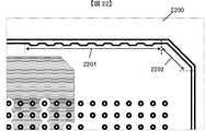
ミアンダ状の配線構造を持つ伝送路をプリント基板2200上に実装した例を図22に示す。図中のコーナーを表す区間2202では、外周の配線長は内周より長いため、スキューが発生する。本実装例では区間2201の配線をミアンダ状にすることによって、スキュー調整を行っている。 An example in which a transmission line having a meander-like wiring structure is mounted on a printed
ミアンダ配線の詳細構造を図20に示す。図中の2008の区間がスキュー調整部のミアンダ配線に該当し、2009と2010は非スキュー調整部を表している。スキュー調整対象の配線の送信端2000から受信端2002までの配線長は、非スキュー調整対象の配線の送信端2001から受信端2003までの配線長よりも長い。このように、差動配線対の片方の配線を引き伸ばすことで、スキュー調整を行なう。 The detailed structure of the meander wiring is shown in FIG. The
しかしながら、この従来のスキュー調整法は、非スキュー調整部と比べ広い差動配線対間の距離2007を持つ凸状の伝送路2004を非スキュー調整部と同じ配線対間の距離2006を持つ伝送路2005と繋ぎ、等間隔に配置するため差動特性インピーダンスの不整合が発生する問題がある。 However, this conventional skew adjustment method uses a
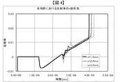
図21は、図20の従来のミアンダ配線構造を持つ差動配線対に、立ち上り時間Tr = 100psecのパルス波を入射したときの反射率を回路シミュレータで解析した結果である。尚、本シミュレーションは、現在広く使われるFR-4基板材料を用いたシンメトリーなストリップ配線を想定し、信号層と接地層の間の距離を0.142mm、非スキュー調整部の差動配線対間の距離2006を0.167mm、凸状の伝送路2004の差動配線対間の距離2007を0.281mm、凸状の伝送路2004の配線長を0.5mm、非スキュー調整部2009、2010の配線長をそれぞれ100mmとした。図中には凸状の伝送路2004が5個、10個、20個と連続して構成した場合の例を示している。図から解るように、スキュー調整を行うことで、凸状の伝送路2004で反射が発生し、またその量は5個、10個、20個と数が増えるごとに、それぞれ0.6%、1.1%、1.2%と大きくなっている。このように従来のミアンダ配線構造でのスキュー調整は差動特性インピーダンスの不整合による反射の影響があり、スキュー調整部が長くなるとその影響は大きくなる。 FIG. 21 is a result of analyzing the reflectance when a pulse wave having a rise time Tr = 100 psec is incident on the differential wiring pair having the conventional meander wiring structure of FIG. 20 using a circuit simulator. This simulation assumes symmetrical strip wiring using the FR-4 board material that is widely used at present, and the distance between the signal layer and the ground layer is 0.142mm, and between the differential wiring pair of the non-skew adjustment part The distance 2006 is 0.167 mm, the
また、従来のミアンダ配線でのスキュー調整ではスキュー調整配線1単位当たりのスキュー調整量が少ないため、スキュー調整には多くの配線エリアを確保する必要がある。 In addition, since the skew adjustment amount per unit of the skew adjustment wiring is small in the skew adjustment in the conventional meander wiring, it is necessary to secure a large wiring area for the skew adjustment.
その他の公知の技術としては、特許文献1による複数の信号層にまたがる差動配線対において、異なった形状をもつビアを実装する方法や、特許文献2による導体部に容量性スタブを実装する方法でのスキュー調整法が提供されているが、これらのいずれの方法においても、電気長調整部分の差動特性インピーダンスの不整合は回避できない。 Other known techniques include a method of mounting vias having different shapes in a differential wiring pair extending over a plurality of signal layers according to
この差動特性インピーダンスの不整合が信号品質に及ぼす影響は、伝送信号の高速化に伴い顕在化してきており、現在、スキュー調整と差動特性インピーダンスの不整合の両方を解決する技術の登場が待たれている。 The effect of this differential characteristic impedance mismatch on signal quality has become apparent as the transmission signal speeds up, and technology that solves both skew adjustment and differential characteristic impedance mismatch has now emerged. I'm waiting.
本発明は、差動特性インピーダンスの整合を保ったままスキュー調整を行い、反射による信号波形の品質劣化を低減する差動信号伝送路を備えたプリント基板を提供することを目的とする。 An object of the present invention is to provide a printed circuit board having a differential signal transmission path that performs skew adjustment while maintaining matching of differential characteristic impedance and reduces quality deterioration of a signal waveform due to reflection.
本発明に係るプリント基板は、好ましくは、平行な差動配線対の部分(以下、非スキュー調整部と呼ぶ。)とスキュー調整用の蛇行状の差動配線対の部分(以下、スキュー調整部と呼ぶ。)とから成る差動信号伝送路を備えたプリント基板において、前記スキュー調整部は、前記非スキュー調整部の差動配線対間の距離に比べ、差動配線対間の距離が広く平行な差動配線対を持つ凸状の伝送路と、差動配線対間の距離が狭く平行な差動配線対を持つ凹状の伝送路の2種類の伝送路を有することを特徴とするプリント基板として構成される。
又、本発明に係るプリント基板は、好ましくは、平行な差動配線対の部分(以下、非スキュー調整部と呼ぶ。)とスキュー調整用の蛇行状の差動配線対の部分(以下、スキュー調整部と呼ぶ。)とから成る差動信号伝送路を備えたプリント基板において、前記スキュー調整部は、前記非スキュー調整部の差動配線対間の距離に比べ、差動配線対間の距離が広く平行な差動配線対を持つ凸状の伝送路と、差動配線対間の距離が狭く平行な差動配線対を持つ直線状の伝送路の2種類の伝送路を有し、スキュー調整対象の配線に、非スキュー調整対象の配線を近づけることを特徴とするプリント基板として構成される。
Theprinted circuit board according to the present inventionpreferably has a parallel differential wiring pair portion (hereinafter referred to as a non-skew adjustment portion) and a meandering differential wiring pair portion for skew adjustment (hereinafter referred to as a skew adjustment portion). In the printed circuit board including the differential signal transmission path, the skew adjustment unit has a larger distance between the differential wiring pairs than the distance between the differential wiring pairs of the non-skew adjustment unit. Aprint having two types of transmission lines: a convex transmission line with parallel differential wiring pairs and a concave transmission line with a parallel differential wiring pair with a short distance between the differential wiring pairs.Configured as a substrate .
The printed circuit board according to the present invention preferably has a parallel differential wiring pair portion (hereinafter referred to as a non-skew adjustment portion) and a meandering differential wiring pair portion for skew adjustment (hereinafter referred to as a skew). In the printed circuit board including the differential signal transmission path, the skew adjustment unit is configured such that the skew adjustment unit has a distance between the differential wiring pair as compared with a distance between the differential wiring pair of the non-skew adjustment unit. There are two types of transmission lines, a convex transmission line with a wide parallel differential wire pair and a straight transmission line with a parallel pair of differential wires with a narrow distance between the differential wire pair, and a skew. The printed circuit board is characterized in that the non-skew adjustment target wiring is brought close to the adjustment target wiring.
本発明の第1の効果は、スキュー調整部と非スキュー調整部の差動特性インピーダンス不整合抑制により信号反射が大幅に低減し、スキュー調整による波形品質劣化を低減できる。 The first effect of the present invention is that signal reflection is greatly reduced by suppressing the differential characteristic impedance mismatch between the skew adjustment unit and the non-skew adjustment unit, and waveform quality deterioration due to skew adjustment can be reduced.
第2の効果は、各々の凸凹区間で差動特性インピーダンスが整合できるため、スキュー調整1区間の配線長制約の緩和、スキュー調整部全体の配線長制約の緩和が可能となる。これにより、設計制約が緩和され、設計品質の向上、及び設計期間の短縮に貢献できる。 The second effect is that differential characteristic impedance can be matched in each uneven section, so that it is possible to alleviate the wiring length restriction in one section of skew adjustment and alleviate the wiring length restriction of the entire skew adjustment section. As a result, the design constraints can be relaxed, and the design quality can be improved and the design period can be shortened.
第3の効果は、配線エリアの省スペース化であり、プリント基板の製造コストを抑制することができる。 The third effect is space saving of the wiring area, and the manufacturing cost of the printed circuit board can be suppressed.
(第1の実施形態)
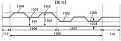
図1は本発明の第1の実施形態を示す正面上視図である。この図は、プリント基板上の差動配線対を表している。図中の112、114が非スキュー調整部、113がスキュー調整部であり、100、101は非スキュー調整部の信号送信側の伝送路、102、103は非スキュー調整部の信号受信側の伝送路である。図中に示されてある通り、送信端の伝送路100は、伝送路104〜108によって受信端の伝送路102に接続されている。このとき、各伝送路を接続する曲げ角は45°以内である事が望ましく、後に述べる本形態以外の場合でも同様である。また、距離109、110、111はそれぞれ、非スキュー調整部112、114における差動配線対間の距離、凹状の伝送路105における作動配線対間の距離、凸状の伝送路107における差動配線対間の距離を表している。距離111は、距離109の2倍以下に抑える事が望ましく、これも後に述べる実施形態にも同様である。以上のようにして本発明の第1の実施形態である、凸凹の差動信号伝送路1区間が構成される。(First embodiment)
FIG. 1 is a front top view showing a first embodiment of the present invention. This figure shows a differential wiring pair on a printed circuit board. In the figure, 112 and 114 are non-skew adjustment units, 113 is a skew adjustment unit, 100 and 101 are transmission paths on the signal transmission side of the non-skew adjustment unit, and 102 and 103 are transmissions on the signal reception side of the non-skew adjustment unit. Road. As shown in the figure, the
図1からわかるように、伝送路の送信端100〜受信端102までの配線長は、伝送路の送信端101〜受信端103までの配線長に比べ長い。このように、本発明の凸凹状の差動配線対を用いることで、差動配線対の片方の配線長を伸ばす事が可能となり、スキュー調整を実施できる。 As can be seen from FIG. 1, the wiring length from the
また、一般的に、差動配線における差動特性インピーダンスは、差動配線対間の距離により変化するため、スキュー調整部113の凸凹の差動配線路1区間における差動特性インピーダンスの平均値が、非スキュー調整部112、114と等しい値になるよう、凸状の伝送路105と凹状の伝送路107の配線長や、差動配線対間の距離110、111を調整し、インピーダンスの整合を保つことにより、入射信号の反射を抑える事が可能となる。さらに、従来のミアンダ配線構造によるスキュー調整に比べて凸凹の差動配線対1区間当たりのスキュー調整量も増える。 In general, the differential characteristic impedance in the differential wiring varies depending on the distance between the pair of differential wirings. Therefore, the average value of the differential characteristic impedance in one section of the uneven differential wiring path of the
尚、図1では凹状の伝送路105を配置した後、凸状の伝送路107を配置する例を示したが、凸状の伝送路107を配置した後、凹状の伝送路105を配置しても本発明の効果を発揮する事ができる。 1 shows an example in which the
(本発明の第1の実施形態を応用した伝送路(1))
図2は、第1の実施形態を応用した伝送路(1)を示す正面上視図である。この図は、プリント基板上の差動配線対を表しており、図1のスキュー調整部113を複数個連続して繋ぎ合わせたものである。図中の210はスキュー調整部である。(Transmission path (1) applying the first embodiment of the present invention)
FIG. 2 is a front top view showing a transmission line (1) to which the first embodiment is applied. This figure shows a differential wiring pair on a printed circuit board, in which a plurality of
本発明の第1実施形態でスキュー調整が完了しない場合は、本形態を用いればよい。第1の実施形態で、スキュー調整部と非スキュー調整部との差動特性インピーダンスの整合がとれているため、凸凹状の伝送路を複数個連続して繋ぎ合わせても、スキュー調整部の差動特性インピーダンスは、非スキュー調整部と等しく保たれる。これにより、設計に課せられる制約が緩和される。 When the skew adjustment is not completed in the first embodiment of the present invention, this embodiment may be used. In the first embodiment, since the differential characteristic impedance of the skew adjustment unit and the non-skew adjustment unit is matched, even if a plurality of uneven transmission lines are continuously connected, the difference between the skew adjustment units The dynamic characteristic impedance is kept equal to that of the non-skew adjustment unit. This alleviates constraints imposed on the design.
図3は、図1のスキュー調整区間を複数個連続させた図2の形態で反射率をシミュレーションした結果を示しており、シミュレーション条件は図21と同じ条件で実施している。差動配線モデルの図1、図20の対応は非スキュー調整部112、114の差動配線対間の距離109は2008と、凸状の伝送路107の差動配線対間の距離111は2009と同じ値を用いている。その他図1の凹状の伝送路105の差動配線対間の距離110を0.115mm、伝送路105、107の配線長をともに0.5mmとした。その結果、図1、2の構成では、図20のように凸凹状の伝送路の数に依存せず、反射率が常に0.1%以下に抑えられ、スキュー調整部の差動インピーダンスが非スキュー調整部の差動インピーダンスと整合していることを示してしている。 FIG. 3 shows the result of simulation of the reflectance in the form of FIG. 2 in which a plurality of skew adjustment sections in FIG. 1 are continued. The simulation conditions are the same as those in FIG. 1 and 20 of the differential wiring model, the
図4は、第1の実施形態を連続して5つ繋ぎ、伝送路105、107の配線長をxとし、xが1mm、2mm、3mmのときに、図3と同じ条件でシミュレーションを実施した結果である。xが増加するとともに反射が目立つようになり、xが2mm以上の場合、入射信号に対する反射が0.3%を超える。この結果から、仮に0.3%に反射を抑えるような設計をしたい場合、立ち上り時間をTr、信号伝播速度をvとしたとき、次式を満たすようにxを選ぶ事が望ましい。 FIG. 4 shows that the simulation was performed under the same conditions as in FIG. 3 when the first embodiment was connected in succession, the wiring length of the

以上のシミュレーションより、本形態は、スキュー調整1区間の配線長の制約緩和、スキュー調整部全体の配線長の制約緩和、安定した差動特性インピーダンス整合の全てを同時に行うことの出来る有効な手段である。 From the above simulation, this embodiment is an effective means that can alleviate the restriction of the wiring length of one skew adjustment section, the restriction of the wiring length of the entire skew adjustment section, and stable differential characteristic impedance matching at the same time. is there.
(第1の実施形態を応用した伝送路(2))
図5は、第1の実施形態を応用した伝送路(2)を示す正面上視図である。
この図は、プリント基板上の差動配線対を表しており、凸状の伝送路500と凹状の伝送路501の配線長がほぼ等しい例である。凸状の伝送路500における差動配線対間の距離504は距離109より広く、凹状の伝送路501における差動配線対間の距離505は距離109より狭い。距離502は距離504と距離109の差分、距離503は距離109と距離505の差分である。(Transmission path using the first embodiment (2))
FIG. 5 is a front top view showing a transmission line (2) to which the first embodiment is applied.
This figure shows a differential wiring pair on a printed circuit board, and is an example in which the wiring lengths of the
スキュー調整部506と非スキュー調整部112、114の差動特性インピーダンスの整合を保つためには、信号の立ち上り時間を100psecと仮定した場合の目安として、距離505をS1、距離109をS、距離504をS2としたとき、以下の式を満足するように設計する事が望ましい。 To maintain the differential characteristic impedance matching between the
(本発明の第1の実施形態を応用した伝送路(3))
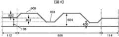
図6は、第1の実施形態を応用した伝送路(3)を示す正面上視図である。この図は、プリント基板上の差動配線対を表しており、凸状の伝送路600の差動配線対間の距離604と距離109の差分602と、凹状の伝送路601の差動配線対間の距離605と距離109の差分603の絶対値がほぼ等しい例である。(Transmission path applying the first embodiment of the present invention (3))
FIG. 6 is a front top view showing a transmission line (3) to which the first embodiment is applied. This figure shows a differential wiring pair on a printed circuit board. The
スキュー調整部606と非スキュー調整部112、114の差動特性インピーダンスの整合を保つ目安として、非スキュー調整部112、114の差動特性インピーダンスをZ、凹状の伝送路601の配線長をx1、差動特性インピーダンスをZ1、凸状の伝送路600の配線長をx2、差動特性インピーダンスをZ2としたとき、以下の式を満足するよう設計することが望ましい。 As a guideline for maintaining the matching of the differential characteristic impedance of the
(第2の実施形態)
図7は、第2の実施形態を示す正面上視図である。この図は、プリント基板上の差動配線対を表しており、非スキュー調整対象の配線をスキュー調整対象の配線に近づけることで差動特性インピーダンスの整合を取ったものである。(Second embodiment)
FIG. 7 is a front top view showing the second embodiment. This figure shows a differential wiring pair on a printed circuit board, in which the differential characteristic impedance is matched by bringing the non-skew adjustment target wiring closer to the skew adjustment target wiring.
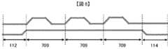
図中の709がスキュー調整部であり、スキュー調整対象の配線は、送信端の伝送路100が伝送路700〜703によって受信端の伝送路102に接続され、非スキュー調整対象の配線は送信端の伝送路101が伝送路704〜706によって受信端の伝送路103に接続されている。伝送路701における差動配線対間の距離707は距離109より広く、伝送路703における差動配線対間の距離708は距離109より狭い。以上のようにして本発明の第2の実施形態である差動信号伝送路1区間が構成される。 In the figure,
このとき、伝送路700、702の配線長を伝送路704、706より長くすることで、その差分からスキューの調整を行う事が出来る。また一般的に、差動配線における差動特性インピーダンスは、差動配線対間の距離に依り変化する。この性質を利用し、スキュー調整部709の差動配線路1区間における差動特性インピーダンスの平均値が、非スキュー調整部112、114と等しい値になるよう、伝送路701、703の配線長や、差動配線対間の距離707、708を調整し、差動特性インピーダンスの整合を保つことによって、入射信号の反射を抑える事が可能となる。 At this time, by making the wiring length of the
(本発明の第2の実施形態を応用した伝送路(1))
図8は、第2の実施形態を応用した伝送路(1)を示す正面上視図である。この図は、プリント基板上の差動配線対を表しており、図7のスキュー調整部709を複数個連続して繋ぎ合わせたものである。第2の実施形態でスキュー調整部709と非スキュー調整部112、114との差動特性インピーダンスの整合がとれているため、複数個連続して繋ぎ合わせてもスキュー調整部全体の差動特性インピーダンスは、非スキュー調整部112、114と等しく保たれる。(Transmission path applying the second embodiment of the present invention (1))
FIG. 8 is a front top view showing a transmission line (1) to which the second embodiment is applied. This figure shows a pair of differential wirings on a printed circuit board, in which a plurality of
本発明の第2の実施形態では配線長が短く、スキュー調整が完了しない場合、本形態がスキュー調整部全体の配線長の制約緩和と差動特性インピーダンス整合を可能とする有効な手段となる。 In the second embodiment of the present invention, when the wiring length is short and the skew adjustment is not completed, the present embodiment is an effective means that enables the relaxation of the wiring length restriction of the entire skew adjustment unit and the differential characteristic impedance matching.
(本発明の第2の実施形態を応用した伝送路(2))
図9は、第2の実施形態を応用した伝送路(2)を示す正面上視図である。この図は、プリント基板上の差動配線対を表しており、伝送路900と伝送路901の配線長がほぼ等しい例である。伝送路900における差動配線対間の距離902は距離109より広く、伝送路901における差動配線対間の距離903は距離109より狭い。(Transmission path applying the second embodiment of the present invention (2))
FIG. 9 is a front top view showing a transmission line (2) to which the second embodiment is applied. This figure shows a differential wiring pair on a printed circuit board, and is an example in which the
スキュー調整部904と非スキュー調整部112、114の差動特性インピーダンスの整合を保つためには、信号の立ち上り時間を100psecと仮定した場合の目安として、距離903をS1、距離109をS、距離902をS2としたとき、(2)式、及び(3)式を満足するように設計する事が望ましい。 To maintain the differential characteristic impedance matching between the
(本発明の第2の実施形態を応用した伝送路(3))
図10は、第2の実施形態を応用した伝送路(3)を示す正面上視図である。この図は、プリント基板上の差動配線対を表しており、伝送路1000の差動配線対間の距離1002と109の差分と、伝送路1001の差動配線対間の距離1003と109の差分の絶対値がほぼ等しい例である。距離1002は距離109より大きく、距離1003は距離109より小さい。(Transmission path applying the second embodiment of the present invention (3))
FIG. 10 is a front top view showing a transmission line (3) to which the second embodiment is applied. This figure shows the differential wiring pair on the printed circuit board. The difference between the
スキュー調整部1004と非スキュー調整部112、114の差動特性インピーダンスの整合を保つ目安として、スキュー調整部112、114の差動特性インピーダンスをZ、伝送路1001の配線長をx1、差動特性インピーダンスをZ1、伝送路1000の配線長をx2、差動特性インピーダンスをZ2としたとき、(4)式を満足するよう設計することが望ましい。 As a guideline for maintaining the differential characteristic impedance matching between the
(第3の実施形態)
図11は、第3の実施形態を示す正面上視図である。この図は、プリント基板上の差動配線対を表しており、配線幅の太さに依って差動特性インピーダンスが変化する性質を利用して、スキュー調整部1108と非スキュー調整部112、114の差動特性インピーダンスの整合を保ったものである。図中に示されてある通り、スキュー調整対象の配線は、送信端の伝送路100が伝送路1100〜1103によって受信端の伝送路102に接続されている。凸状の伝送路1101の差動配線対間の距離1106は距離109より広く、凹状の伝送路1103の差動配線対間の距離1107は距離109より狭い。また、スキュー調整部1108において、非スキュー調整部112、114に比べ、凸状の伝送路1101の配線幅は太く、凹状の伝送路1103の配線幅は細い。非スキュー調整対象の配線も、少なくともスキュー調整対象の配線と平行な配線長だけ、伝送路1104の配線幅の太さを凸状伝送路1101に、伝送路1105の配線幅の太さを凹状の伝送路1103に合わせ、シングルエンドの特性インピーダンスを共に一致させる。以上のようにして本発明の第3の実施形態である差動信号伝送路1区間が構成される。(Third embodiment)
FIG. 11 is a front top view showing the third embodiment. This figure shows a differential wiring pair on a printed circuit board, and a
凸状の伝送路1101と凹状の伝送路1103の配線長や太さ、距離1106、1107を調節すれば、スキュー調整部1108の差動特性インピーダンスと非スキュー調整部112、114の差動特性インピーダンスの整合を保てるため、本形態でもスキュー調整と差動特性インピーダンス整合の両方を実現する事が出来る。 By adjusting the wiring length and thickness of the
(第3の実施形態を応用した伝送路(1))
図12は、第3の実施形態を応用した伝送路(1)を示す正面上視図である。この図は、プリント基板上の差動配線対を表しており、第3の実施形態を複数個連続して繋ぎ合わせたものである。第3の実施形態でスキュー調整部112、114と非スキュー調整部1108との差動特性インピーダンスの整合がとれているため、複数個連続して繋ぎ合わせても、スキュー調整部全体の差動特性インピーダンスは、非スキュー調整部112、114と等しく保たれる。(Transmission path using the third embodiment (1))
FIG. 12 is a front top view showing a transmission line (1) to which the third embodiment is applied. This figure shows a pair of differential wirings on a printed circuit board, and a plurality of third embodiments are continuously connected. In the third embodiment, since the differential characteristic impedances of the
本発明の第3の実施形態では配線長が短く、スキュー調整が完了しない場合、本形態がスキュー調整部全体の配線長の制約緩和と差動特性インピーダンス整合を可能とする有効な手段となる。 In the third embodiment of the present invention, when the wiring length is short and the skew adjustment is not completed, the present embodiment is an effective means that enables the relaxation of the wiring length restriction of the entire skew adjustment unit and the differential characteristic impedance matching.
(第3の実施形態を応用した伝送路(2))
図13は、第3の実施形態を応用した伝送路(2)を示す正面上視図である。
この図は、プリント基板上の差動配線対を表しており、凸状の伝送路1300と凹状の伝送路1301の配線長がほぼ等しい例である。スキュー調整対象の配線において、凸状の伝送路1300は、差動配線対間の距離1304が距離109より広く、配線幅が非スキュー調整部112、114より太い。また、凹状の伝送路1301は、差動配線対間の距離1305が距離109より狭く、配線幅が非スキュー調整部112、114より細い。非スキュー調整対象の配線も、少なくともスキュー調整対象の配線と平行な配線長だけ、伝送路1302の配線幅の太さを凸状の伝送路1300に、伝送路1303の配線幅の太さを凹状の伝送路1301に合わせ、シングルエンドのインピーダンスを共に一致させる。(Transmission path using the third embodiment (2))
FIG. 13 is a front top view showing a transmission line (2) to which the third embodiment is applied.
This figure shows a differential wiring pair on a printed circuit board, and is an example in which the wiring lengths of the
この形態においても、スキュー調整部1306における配線幅の太さ、距離1304、1305を調整することで、非スキュー調整部112、114との差動特性インピーダンスの整合を保つ事が出来る。 Also in this embodiment, by adjusting the width of the wiring width and the
(第3の実施形態を応用した伝送路(3))
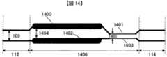
図14は、第3の実施形態を応用した伝送路(3)を示す正面上視図である。この図は、プリント基板上の差動配線対を表しており、凸状の伝送路1400の差動配線対間の距離1404と距離109の差分と、距離109と凹状の伝送路1401の差動配線対間との距離1405の差分の絶対値がほぼ等しい例である。スキュー調整対象の配線において、凸状の伝送路1400は、差動配線対間の距離1404が距離109より広く、配線幅が非スキュー調整部112、114より太い。また、凹状の伝送路1400は、差動配線対間の距離1305が距離109より狭く、配線幅が非スキュー調整部112、114より細い。非スキュー調整対象の配線も、少なくともスキュー調整対象の配線と平行な配線長だけ、伝送路1402の配線幅の太さを凸状の伝送路1400に、伝送路1403の配線幅の太さを凹状の伝送路1401に合わせ、シングルエンドのインピーダンスを共に一致させる。(Transmission path using the third embodiment (3))
FIG. 14 is a front top view showing a transmission line (3) to which the third embodiment is applied. This figure shows the differential wiring pair on the printed circuit board, the difference between the
この形態においても、スキュー調整部1406における配線幅の太さ、凸状の伝送路1400、凹状の伝送路1401の配線長を調整することで、非スキュー調整部112、114との差動特性インピーダンスの整合を保つ事が出来る。 Also in this embodiment, the differential characteristic impedance with respect to the
(第4の実施形態)
図15は、第4の実施形態を示す正面上視図である。この図は、プリント基板上の差動配線対を表しており、スキュー調整部1505は、凸状の伝送路1500、伝送路1501、凸状伝送路1508を接続した区間1506と、凹状の伝送路1502、伝送路1501、凹状の伝送路1509を接続した区間1507から構成される。凸状の伝送路1500、1508における差動配線対間の距離1503は距離109より広く、伝送路1501における差動配線対間の距離は距離109と等しく、凹状の伝送路1502、1509における差動配線対間の距離1504は距離109より狭い。以上のようにして本発明の第4の実施形態である差動信号伝送路1区間が構成される。(Fourth embodiment)
FIG. 15 is a front top view showing the fourth embodiment. This figure shows a differential wiring pair on a printed circuit board. The
ここで、非スキュー調整部112、114に比べ、区間1506の差動特性インピーダンスは高く、 区間1507の差動特性インピーダンスは低い。この性質を利用し、スキュー調整部1505の差動特性インピーダンスの平均値が非スキュー調整部112、114と等しくなるよう、凸状の伝送路1500、1508、凹状の伝送路1502、1509の配線長や、距離1503、1504を調整する。このように、本形態でもスキュー調整と差動特性インピーダンス整合の両方を実現する事が出来る。 Here, the differential characteristic impedance in the
但し、区間1506、1507の配線長が、(1)式のxを満たすように設計することが必要である。 However, it is necessary to design the wiring lengths of the
また、図中には、凸状の伝送路を2つ、凹状の伝送路を2つ接続した例を示したが、2つ以上の凸状の伝送路、凹状の伝送路が続く場合でも、配線長1506、1507が(1)式を満足する限り、同様の効果を発揮する事が出来る。 In addition, in the figure, an example in which two convex transmission paths and two concave transmission paths are connected is shown, but even when two or more convex transmission paths and concave transmission paths continue, As long as the
(第4の実施形態を応用した伝送路(1))
図16は、第4の実施形態を応用した伝送路(1)を示す正面上視図である。この図は、プリント基板上の差動配線対を表しており、図15のスキュー調整部1505を複数個連続して繋ぎ合わせたものである。第4の実施形態におけるスキュー調整部1505と非スキュー調整部112、114でインピーダンスの整合がとれているため、複数個連続して繋ぎ合わせても、スキュー調整部全体の差動特性インピーダンスは、非スキュー調整部112、114と等しく保たれる。(Transmission path using the fourth embodiment (1))
FIG. 16 is a front top view showing a transmission line (1) to which the fourth embodiment is applied. This figure shows a pair of differential wirings on a printed circuit board, in which a plurality of
本発明の第4実施形態では配線長が短く、スキュー調整が完了しない場合、本形態が長距離にわたるスキュー調整と差動特性インピーダンス整合を可能とする有効な手段となる。 In the fourth embodiment of the present invention, when the wiring length is short and skew adjustment is not completed, this embodiment is an effective means for enabling skew adjustment and differential characteristic impedance matching over a long distance.
(第4の実施形態を応用した伝送路(2))
図17は、第4の実施形態を応用した伝送路(2)を示す正面上視図である。この図は、プリント基板上の差動配線対を表しており、凸状の伝送路1700と凹状の伝送路1702の配線長がほぼ等しい例である。凸状の伝送路1700における差動配線対間の距離1703は距離109より広く、凹状の伝送路1702における差動配線対間の距離1704は距離109より狭い。1701は非スキュー調整部112、114と同じ配線対間の距離109を持つ伝送路を表す。1706は差動特性インピーダンスが高い区間、1707は差動特性インピーダンスが低い区間である。(Transmission path using the fourth embodiment (2))
FIG. 17 is a front top view showing a transmission line (2) to which the fourth embodiment is applied. This figure shows a differential wiring pair on a printed circuit board, and is an example in which the wiring lengths of the
スキュー調整部1705と非スキュー調整部112、114の差動特性インピーダンスの整合を保つためには、信号の立ち上り時間を100psecと仮定した場合の目安として、距離1704をS1、距離109をS、距離1703をS2としたとき、(2)式、及び(3)式を満足するように設計する事が望ましい。 To maintain the differential characteristic impedance matching between the
(第4の実施形態を応用した伝送路(3))
図18は、第4の実施形態を応用した伝送路(3)を示す正面上視図である。この図は、プリント基板上の差動配線対を表しており、凸状の伝送路1800の差動配線対間の距離1803と距離109の差分、距離109と凹伝送路1802の差動配線対間との距離1804の差分がほぼ等しい例である。凸状の伝送路1800における差動配線対間の距離1803は距離109より広く、凹状の伝送路1802における差動配線対間の距離1804は距離109より狭い。1801は非スキュー調整部と同じ差動配線対間の距離109を持つ伝送路を表す。1806は差動特性インピーダンスが高い区間、1807は差動特性インピーダンスが低い区間である。(Transmission path using the fourth embodiment (3))
FIG. 18 is a front top view showing a transmission line (3) to which the fourth embodiment is applied. This figure shows the differential wiring pair on the printed circuit board, and the difference between the
スキュー調整部1805と非スキュー調整部112、114の差動特性インピーダンスの整合を保つ目安として、非スキュー調整部の差動特性インピーダンスをZ、凹状の伝送路1802の配線長をx1、差動特性インピーダンスをZ1、凸状の伝送路1800の配線長をx2、差動特性インピーダンスをZ2としたとき、(4)式を満足するよう設計することが望ましい。 As a guideline for maintaining the differential characteristic impedance matching between the
(第5の実施形態)
図19は、第5の実施形態を示す正面上視図である。この図は、プリント基板上の差動配線対を表しており、ミアンダ状の配線構造を持つ区間1906で上昇した差動特性インピーダンスを下げる目的で、凹状の伝送路1902を持つ区間1907を接続したものである。(Fifth embodiment)
FIG. 19 is a front top view showing the fifth embodiment. This figure shows a differential wiring pair on a printed circuit board, and a
凸状の伝送路1900における差動配線対間の距離1903は距離109より広く、凹状の伝送路1902における差動配線対間の距離1904は距離109より狭い。1901は非スキュー調整部112、114と同じ配線対間の距離109を持つ伝送路を表す。 The
スキュー調整は、凸状の伝送路1900と伝送路1901を交互に繋げた1906の区間で行い、スキュー調整により上昇したインピーダンスを、凹状の伝送路1902を配置した1907の区間で下げ、非スキュー調整部112、114とスキュー調整部1905の差動特性インピーダンスの整合を保つ。以上のようにしても、スキュー調整と信号反射低減の両方を実現することができる。 Skew adjustment is performed in the 1906 section where the
但し、1906、1907の区間の配線長が、(1)式のx を満たすように設計する事が必要である。 However, it is necessary to design the wiring length of the
また、図には、凸状の伝送路を3つ接続した例を示しているが、凸状の伝送路が3つ以上の場合も、区間1906、1907の配線長の配線長が(2)式のxより小さな値であれば適用可能である。 In addition, the figure shows an example in which three convex transmission lines are connected. However, when there are three or more convex transmission lines, the wiring length of
さらに、図19とは逆に、凹状の伝送路1902をスキュー調整に使い、凸上の伝送路1900を下降した差動特性インピーダンスの整合をとる目的で使用しても、区間1906、1907の配線長の配線長が(1)式を満足していれば、同様の効果を発揮できる。 Further, contrary to FIG. 19, even if the
以上述べた全ての実施例は、種々の材料を使用したプリント基板にて実現でき、例えば信号層、接地層は銅や金などの金属導体が好適である。また図示していないが、信号層、接地層間には誘電体層が形成される。この誘電体層はガラスエポキシやポリテトラフルオロエチレン、ポリイミド、セラミック等の材料が好適である。もちろん、前述した導体、誘電体に限らず、他の材料を使用してもよい。さらに、図中でストリップ配線、マイクロストリップ配線等の明示をしていないが、本発明の効果は、どちらの構造においても享受することができる。 All the embodiments described above can be realized by a printed circuit board using various materials. For example, the signal layer and the ground layer are preferably metal conductors such as copper and gold. Although not shown, a dielectric layer is formed between the signal layer and the ground layer. The dielectric layer is preferably made of a material such as glass epoxy, polytetrafluoroethylene, polyimide, or ceramic. Of course, other materials are not limited to the conductors and dielectrics described above. Furthermore, although strip wiring, microstrip wiring, etc. are not clearly shown in the figure, the effects of the present invention can be enjoyed in either structure.
また、1つの伝送路上において、上記実施例の複数を組み合わせて使用することも可能である。 In addition, a plurality of the above embodiments can be used in combination on one transmission line.
そして、これらの実施例は、凸状の伝送路と凹状の伝送路を設けるということ以外、一般的なプリント基板に用いられている配線構造と同じである。差動配線対間の距離、配線幅の太さを調整することで容易に実現できるので、一般的なプリント基板の製造工程を適用して製造する事ができる。従って、以上述べた実施例は全て高コストとなる特別な工程を使用することなく実現できる。 These embodiments are the same as the wiring structure used for a general printed circuit board except that a convex transmission path and a concave transmission path are provided. Since it can be easily realized by adjusting the distance between the differential wiring pair and the thickness of the wiring width, it can be manufactured by applying a general printed circuit board manufacturing process. Therefore, all of the embodiments described above can be realized without using a special process that is expensive.
100 スキュー調整対象の配線における送信側の伝送路
101 非スキュー調整対象の配線における送信側の伝送路
102 スキュー調整対象の配線における受信側の伝送路
103 非スキュー調整対象の配線における受信側の伝送路
104 100と105を繋ぎ、スキュー調整を行う伝送路
105 非スキュー調整部に比べ狭い差動配線対間の距離を持つ凹状の伝送路
106 105と107を繋ぎ、スキュー調整を行う伝送路
107 非スキュー調整部に比べ広い差動配線対間の距離を持つ凸状の伝送路
108 107と102を繋ぎ、スキュー調整を行う伝送路
109 非スキュー調整部における差動配線対間の距離
110 凹状の伝送路105における差動配線対間の距離
111 凸上の伝送路107における差動配線対間の距離
112 送信側の非スキュー調整部
113 スキュー調整部
114 受信側の非スキュー調整部
210 ミアンダ状の配線構造を持つ差動配線対におけるスキュー調整部
500 非スキュー調整部に比べ広い差動配線対間の距離を持つ501と等しい配線長の凸状の伝送路
501 非スキュー調整部に比べ狭い差動配線対間の距離を持つ500と等しい配線長の凹状の伝送路
502 504と109の差分の距離
503 109と505の差分の距離
504 凸上の伝送路500における差動配線対間の距離
505 凹状の伝送路501における差動配線対間の距離
506 スキュー調整部
600 非スキュー調整部に比べ広い差動配線対間の距離を持つ601より長い配線長の凸状の伝送路
601 非スキュー調整部に比べ狭い差動配線対間の距離を持つ600より長い配線長凹状の伝送路
602 604と109の差分の距離
603 109と605の差分の距離
604 凸状の伝送路600における差動配線対間の距離
605 凹状の伝送路601における差動配線対間の距離
606 スキュー調整部
700 非スキュー調整部112と701を繋ぎ、スキュー調整を行う伝送路
701 非スキュー調整部に比べ広い差動配線対間の距離を持つ伝送路
702 701と703を繋ぎ、スキュー調整を行う伝送路
703 非スキュー調整部に比べ狭い差動配線対間の距離を持つ伝送路
704 非スキュー調整部112と705を繋ぐ伝送路
705 スキュー調整対象の配線に近づけた伝送路
706 705と非スキュー調整部114を繋ぐ伝送路
707 伝送路701における差動配線対間の距離
708 伝送路703における差動配線対間の距離
709 スキュー調整部
900 非スキュー調整部に比べ広い差動配線対間の距離を持つ901と等しい配線長の伝送路
901 非スキュー調整部に比べ狭い差動配線対間の距離を持つ900と等しい配線長の伝送路
902 伝送路900における差動配線対間の距離
903 伝送路901における差動配線対間の距離
904 スキュー調整部
1000 非スキュー調整部に比べ広い差動配線対間の距離を持つ1001より長い配線長の伝送路
1001 非スキュー調整部に比べ狭い差動配線対間の距離を持つ1000より短い配線長の伝送路
1002 伝送路1000における差動配線対間の距離
1003 伝送路1001における差動配線対間の距離
1004 スキュー調整部
1100 スキュー調整部112と1101を繋ぎ、スキュー調整を行う伝送路
1101 非スキュー調整部に比べ広い差動配線対間の距離を持ち、112、114より配線幅が太い凸状の伝送路
1102 1101と1103を繋ぎ、スキュー調整を行う伝送路
1103 非スキュー調整部に比べ狭い差動配線対間の距離を持ち、112、114より配線幅が細い凹状の伝送路
1104 配線幅の太い伝送路
1105 配線幅の細い伝送路
1106 凸状の伝送路1101における配線対間の距離
1107 凹状の伝送路1103における配線対間の距離
1108 スキュー調整部
1300 非スキュー調整部に比べ広い差動配線対間の距離を持ち、112、114より配線幅が太い1301と同じ配線長の凸状の伝送路
1301 非スキュー調整部に比べ広い差動配線対間の距離を持ち、112、114より配線幅が細い1300と同じ配線長の凹状の伝送路
1302 配線幅の太い伝送路
1303 配線幅の細い伝送路
1400 非スキュー調整部に比べ広い差動配線対間の距離を持ち、112、114より配線幅が太く、1301より長い配線長の凸状の伝送路
1401 非スキュー調整部に比べ広い差動配線対間の距離を持ち、112、114より配線幅が細く、1400より長い配線長の凸状の伝送路
1402 配線幅の太い伝送路
1403 配線幅の細い伝送路
1404 凸状の伝送路1400における差動配線対間の距離
1405 凹状の伝送路1401における差動配線対間の距離
1406 スキュー調整部
1500 非スキュー調整部に比べ広い差動配線対間の距離を持つ凸状の伝送路
1501 非スキュー調整部と同じ差動配線対間の距離を持つ伝送路
1502 非スキュー調整部に比べ狭い差動配線対間の距離を持つ凹状の伝送路
1503 凸状の伝送路1500における差動配線対間の距離
1504 凹状の伝送路1501における差動配線対間の距離
1505 スキュー調整部
1506 非スキュー調整部に比べ差動特性インピーダンスの高い区間
1507 非スキュー調整部に比べ差動特性インピーダンスの低い区間
1508 非スキュー調整部に比べ広い差動配線対間の距離を持つ凸状の伝送路
1509 非スキュー調整部に比べ狭い差動配線対間の距離を持つ凹状の伝送路
1700 非スキュー調整部に比べ広い差動配線対間の距離を持つ1702と同じ配線長の凸状の伝送路
1701 非スキュー調整部と同じ差動配線対間の距離を持つ伝送路
1702 非スキュー調整部に比べ狭い差動配線対間の距離を持つ1700と同じ配線長の凹状の伝送路
1703 凸状の伝送路1700における差動配線対間の距離
1704 凹状の伝送路1702における差動配線対間の距離
1705 スキュー調整部
1706 非スキュー調整部に比べ差動特性インピーダンスの高い区間
1707 非スキュー調整部に比べ差動特性インピーダンスの低い区間
1800 非スキュー調整部に比べ広い差動配線対間の距離を持つ1802より配線長の長い凸状の伝送路
1801 非スキュー調整部と同じ差動配線対間の距離を持つ伝送路
1802 非スキュー調整部に比べ広い差動配線対間の距離を持つ1800より配線長の短い凹状の伝送路
1803 凸状の伝送路1800における差動配線対間の距離
1804 凹状の伝送路1802における差動配線対間の距離
1805 スキュー調整部
1806 非スキュー調整部に比べ差動特性インピーダンスの高い区間
1807 非スキュー調整部に比べ差動特性インピーダンスの低い区間
1900 非スキュー調整部に比べ広い差動配線対間の距離を持つ凸状の伝送路
1901 非スキュー調整部と同じ差動配線対間の距離を持つ伝送路
1902 非スキュー調整部に比べ広い差動配線対間の距離を持つ凹状の伝送路
1903 凸状の伝送路1900における差動配線対間の距離
1904 凹状の伝送路1902における差動配線対間の距離
1905 スキュー調整部
1906 非スキュー調整部に比べ差動特性インピーダンスの高い区間
1907 非スキュー調整部に比べ差動特性インピーダンスの低い区間
2000 スキュー対象配線の送信端
2001 非スキュー対象配線の送信端
2002 スキュー調整対象配線の受信端
2003 非スキュー調整対象の配線の受信端
2004 非スキュー調整部に比べ広い差動配線対間の距離を持つ凸状の伝送路
2005 非スキュー調整部と同じ差動配線対間の距離を持つ伝送路
2006 非スキュー調整部の差動配線対間の距離
2007 凸状の伝送路2004における差動配線対間の距離
2008 スキュー調整部
2009 送信側の非スキュー調整部
2010 受信側の非スキュー調整部
2200 プリント基板
2201 スキュー調整のためミアンダ配線を施した区間
2202 スキューが発生するコーナーの区間100 Transmission path on the sending side of the wiring for skew adjustment
101 Transmission path on the transmission side of the non-skewed wiring
102 Transmission path on the receiving side of the wiring for skew adjustment
103 Transmission path on the receiving side of the non-skewed wiring
104 Transmission path connecting 100 and 105 to adjust skew
105 Concave transmission line with a narrower distance between differential wire pairs than the non-skew adjuster
106 Transmission
107 Convex transmission line with wider distance between differential wiring pairs than non-skew adjustment unit
108 Transmission path connecting 107 and 102 to adjust skew
109 Distance between differential wiring pair in non-skew adjustment section
110 Distance between differential wiring pair in
111 Distance between differential wiring pairs on
112 Non-skew adjustment section on transmission side
113 Skew adjustment section
114 Non-skew adjuster at receiver
210 Skew adjuster in differential wiring pair with meandering wiring structure
500 Convex transmission line with a wiring length equal to 501 with a wider distance between differential wiring pairs than the non-skew adjustment section
501 Concave transmission line with a wiring length equal to 500 with a narrower distance between differential wiring pairs than the non-skew adjustment unit
502 Distance between 504 and 109
503 Difference distance between 109 and 505
504 Distance between differential wiring pairs in
505 Distance between differential wiring pairs in
506 Skew adjuster
600 Convex transmission line with longer wiring length than 601 with wider distance between differential wiring pairs than non-skew adjuster
601 Longer than 600 transmission lines with a narrower distance between differential wiring pairs than non-skew adjuster
602 Difference distance between 604 and 109
603 Difference distance between 109 and 605
604 Distance between differential wiring pair in
605 Distance between differential wiring pair in
606 Skew adjustment unit
700 Transmission path connecting
701 Transmission path with wider distance between differential wiring pairs than non-skew adjustment unit
702 Transmission path connecting 701 and 703 to adjust skew
703 Transmission path with narrower distance between differential wiring pair than non-skew adjustment unit
704 Transmission path connecting
705 Transmission path close to the wiring for skew adjustment
Transmission line connecting 706 705 and
707 Distance between differential wiring pair in
708 Distance between differential wiring pair in
709 Skew adjuster
900 Transmission line with a wiring length equal to 901 with a wider distance between differential wiring pairs than the non-skew adjustment section
901 Transmission path with a wire length equal to 900, with a narrower distance between differential wire pairs than the non-skew adjuster
902 Distance between differential wiring pair in transmission line 900
903 Distance between differential wiring pair in
904 Skew adjustment unit
1000 Transmission path longer than 1001 with a wider distance between differential wiring pairs than non-skew adjuster
1001 Transmission path with a wiring length shorter than 1000 with a narrower distance between differential wiring pairs than the non-skew adjustment section
1002 Distance between differential wiring pair in
1003 Distance between differential wiring pair in
1004 Skew adjustment section
1100 Transmission path connecting
1101 Convex transmission line with a wider distance between differential wiring pairs than the non-skew adjustment section and wider wiring width than 112 and 114
1102 Transmission path connecting 1101 and 1103 to adjust skew
1103 A concave transmission line that has a narrower distance between the pair of differential wires than the non-skew adjuster and a narrower wire width than 112 and 114
1104 Transmission line with wide wiring width
1105 Transmission line with narrow wiring width
1106 Distance between wiring pairs in
1107 Distance between wiring pairs in
1108 Skew adjuster
1300 Convex transmission line with the same wiring length as 1301, which has a wider distance between differential wiring pairs than the non-skew adjustment section and has a wiring width wider than 112 and 114
1301 A concave transmission line with the same wiring length as 1300, which has a wider distance between differential wiring pairs than the non-skew adjustment unit and whose wiring width is narrower than 112 and 114
1302 Transmission line with wide wiring width
1303 Transmission line with narrow wiring width
1400 Convex transmission line with wider distance between differential wiring pairs than non-skew adjustment unit, wiring width wider than 112, 114, and wiring length longer than 1301
1401 A convex transmission line with a wider distance between differential wiring pairs than the non-skew adjustment unit, a wiring width narrower than 112, 114, and a wiring length longer than 1400
1402 Transmission line with wide wiring width
1403 Transmission line with narrow wiring width
1404 Distance between differential wiring pair in
1405 Distance between differential wiring pair in
1406 Skew adjuster
1500 Convex transmission line with wider distance between differential wiring pairs than non-skew adjustment unit
1501 Transmission line with the same distance between the differential wiring pair as the non-skew adjustment unit
1502 Concave transmission line with narrower distance between differential wiring pair than non-skew adjustment part
1503 Distance between differential wiring pairs in
1504 Distance between differential wiring pair in
1505 Skew adjuster
1506 Section with higher differential characteristic impedance than non-skew adjuster
1507 Section with lower differential characteristic impedance than non-skew adjustment section
1508 Convex transmission line with a wider distance between differential wire pairs than non-skew adjuster
1509 Concave transmission line with a narrower distance between differential wire pairs than non-skew adjuster
1700 Convex transmission line with the same wiring length as 1702, which has a wider distance between differential wiring pairs than the non-skew adjustment unit
1701 Transmission path with the same distance between the differential wiring pair as the non-skew adjuster
1702 Concave transmission line with the same wiring length as 1700, which has a narrower distance between differential wiring pairs than the non-skew adjustment unit
1703 Distance between differential wiring pair in
1704 Distance between differential wiring pair in
1705 Skew adjuster
1706 Section with higher differential characteristic impedance than non-skew adjuster
1707 Section with lower differential characteristic impedance than non-skew adjuster
1800 Convex transmission line with longer wiring length than 1802 with wider distance between differential wiring pairs than non-skew adjuster
1801 Transmission path with the same distance between differential wiring pairs as the non-skew adjustment section
1802 Concave transmission line with a shorter wiring length than 1800, which has a wider distance between differential wiring pairs than the non-skew adjustment unit
1803 Distance between differential wiring pair in
1804 Distance between differential wiring pair in
1805 Skew adjuster
1806 Section with higher differential characteristic impedance than non-skew adjuster
1807 Section with lower differential characteristic impedance than non-skew adjuster
1900 Convex transmission line with a wider distance between differential wire pairs than non-skew adjuster
1901 Transmission line with the same distance between the differential wiring pair as the non-skew adjustment unit
1902 Concave transmission line with a wider distance between differential wire pairs than non-skew adjuster
1903 Distance between differential wiring pairs in
1904 Distance between differential wiring pair in
1905 Skew adjustment section
1906 Section with higher differential characteristic impedance than non-skew adjuster
1907 Section with lower differential characteristic impedance than non-skew adjuster
2000 Sending end of skew target wiring
2001 Transmission end of unskewed wiring
2002 Reception end of wiring for skew adjustment
2003 Non-skew adjustment target receiving end
2004 Convex transmission line with a wider distance between differential wire pairs than non-skew adjuster
2005 Transmission path with the same distance between differential wiring pairs as the non-skew adjuster
2006 Distance between differential wiring pairs in non-skew adjustment section
2007 Distance between differential wiring pairs in
2008 Skew adjustment section
2009 Non-skew adjustment section on the transmission side
2010 Non-skew adjuster on receiver
2200 PCB
2201 Section with meander wiring for skew adjustment
2202 Corner section where skew occurs
Claims (15)
Translated fromJapanese配置することを特徴とする請求項5記載のプリント基板。6. The printed circuit board according to claim 5, wherein a plurality of two types of transmission lines having different distances between the differential wiring pairs of the skew adjusting unit are continuously arranged.
Priority Applications (3)
| Application Number | Priority Date | Filing Date | Title |
|---|---|---|---|
| JP2010039560AJP5427644B2 (en) | 2010-02-25 | 2010-02-25 | Printed board |
| US12/985,765US9024196B2 (en) | 2010-02-25 | 2011-01-06 | Different signal transmission line for printed circuit board |
| CN201110006583.5ACN102170749B (en) | 2010-02-25 | 2011-01-10 | Printed circuit board |
Applications Claiming Priority (1)
| Application Number | Priority Date | Filing Date | Title |
|---|---|---|---|
| JP2010039560AJP5427644B2 (en) | 2010-02-25 | 2010-02-25 | Printed board |
Publications (2)
| Publication Number | Publication Date |
|---|---|
| JP2011176151A JP2011176151A (en) | 2011-09-08 |
| JP5427644B2true JP5427644B2 (en) | 2014-02-26 |
Family
ID=44475540
Family Applications (1)
| Application Number | Title | Priority Date | Filing Date |
|---|---|---|---|
| JP2010039560AExpired - Fee RelatedJP5427644B2 (en) | 2010-02-25 | 2010-02-25 | Printed board |
Country Status (3)
| Country | Link |
|---|---|
| US (1) | US9024196B2 (en) |
| JP (1) | JP5427644B2 (en) |
| CN (1) | CN102170749B (en) |
Families Citing this family (41)
| Publication number | Priority date | Publication date | Assignee | Title |
|---|---|---|---|---|
| JP2011113575A (en)* | 2009-11-24 | 2011-06-09 | Hitachi Consumer Electronics Co Ltd | Flexible printed board and electric apparatus and optical disk drive using the same |
| JP5466557B2 (en)* | 2010-03-29 | 2014-04-09 | 日本シイエムケイ株式会社 | Printed wiring board with differential wiring |
| USD701843S1 (en)* | 2010-12-28 | 2014-04-01 | Sumitomo Electric Industries, Ltd. | Semiconductor device |
| US8835775B2 (en)* | 2011-11-15 | 2014-09-16 | Cisco Technology, Inc. | Localized skew compensation technique for reducing electromagnetic radiation |
| US9674086B2 (en) | 2013-11-05 | 2017-06-06 | Cisco Technology, Inc. | Work conserving schedular based on ranking |
| US10778584B2 (en) | 2013-11-05 | 2020-09-15 | Cisco Technology, Inc. | System and method for multi-path load balancing in network fabrics |
| US10951522B2 (en) | 2013-11-05 | 2021-03-16 | Cisco Technology, Inc. | IP-based forwarding of bridged and routed IP packets and unicast ARP |
| US9655232B2 (en) | 2013-11-05 | 2017-05-16 | Cisco Technology, Inc. | Spanning tree protocol (STP) optimization techniques |
| US9769078B2 (en) | 2013-11-05 | 2017-09-19 | Cisco Technology, Inc. | Dynamic flowlet prioritization |
| US9825857B2 (en) | 2013-11-05 | 2017-11-21 | Cisco Technology, Inc. | Method for increasing Layer-3 longest prefix match scale |
| US9397946B1 (en) | 2013-11-05 | 2016-07-19 | Cisco Technology, Inc. | Forwarding to clusters of service nodes |
| US9876711B2 (en) | 2013-11-05 | 2018-01-23 | Cisco Technology, Inc. | Source address translation in overlay networks |
| US9374294B1 (en) | 2013-11-05 | 2016-06-21 | Cisco Technology, Inc. | On-demand learning in overlay networks |
| US9502111B2 (en) | 2013-11-05 | 2016-11-22 | Cisco Technology, Inc. | Weighted equal cost multipath routing |
| US9509092B2 (en)* | 2013-11-06 | 2016-11-29 | Cisco Technology, Inc. | System and apparatus for network device heat management |
| CN104039076A (en)* | 2014-06-17 | 2014-09-10 | 浪潮(北京)电子信息产业有限公司 | Wire wrapping method and system for reducing difference circuit impedance mismatch degree |
| US9118516B1 (en) | 2014-08-29 | 2015-08-25 | International Business Machines Corporation | Differential transmission line with common mode notch filter |
| US9479362B2 (en) | 2014-08-29 | 2016-10-25 | Lenovo Enterprise Solutions (Singapore) Pte. Ltd. | Differential transmission line with common mode notch filter |
| US10116493B2 (en) | 2014-11-21 | 2018-10-30 | Cisco Technology, Inc. | Recovering from virtual port channel peer failure |
| CN105338732A (en)* | 2015-12-09 | 2016-02-17 | 浪潮电子信息产业股份有限公司 | Winding method for improving high-speed differential signal |
| JP6620565B2 (en)* | 2016-01-20 | 2019-12-18 | セイコーエプソン株式会社 | Printed wiring board, information communication device, and display system |
| US10142163B2 (en) | 2016-03-07 | 2018-11-27 | Cisco Technology, Inc | BFD over VxLAN on vPC uplinks |
| US10333828B2 (en) | 2016-05-31 | 2019-06-25 | Cisco Technology, Inc. | Bidirectional multicasting over virtual port channel |
| US11509501B2 (en) | 2016-07-20 | 2022-11-22 | Cisco Technology, Inc. | Automatic port verification and policy application for rogue devices |
| JP2018037463A (en)* | 2016-08-29 | 2018-03-08 | 京セラ株式会社 | Printed wiring board |
| US10193750B2 (en) | 2016-09-07 | 2019-01-29 | Cisco Technology, Inc. | Managing virtual port channel switch peers from software-defined network controller |
| CN106507583A (en)* | 2016-10-25 | 2017-03-15 | 郑州云海信息技术有限公司 | A signal transmission line, method and system |
| JP6847814B2 (en)* | 2017-06-16 | 2021-03-24 | 京セラ株式会社 | Printed wiring board |
| US10547509B2 (en) | 2017-06-19 | 2020-01-28 | Cisco Technology, Inc. | Validation of a virtual port channel (VPC) endpoint in the network fabric |
| JP6834830B2 (en)* | 2017-07-25 | 2021-02-24 | セイコーエプソン株式会社 | Integrated circuit equipment, physical quantity measuring equipment, electronic devices and mobile objects |
| JP2019024560A (en)* | 2017-07-25 | 2019-02-21 | 株式会社三共 | Game machine |
| US10485096B2 (en)* | 2017-11-29 | 2019-11-19 | Dell Products L.P. | Differential trace pair system |
| CN108055760B (en)* | 2017-12-29 | 2021-01-19 | 深圳市兴森快捷电路科技股份有限公司 | Differential pair equal-length compensation impedance matching method |
| US10306749B1 (en)* | 2018-02-19 | 2019-05-28 | Dell Products L.P. | System and method of utilizing serpentine regions |
| JP6697508B2 (en)* | 2018-05-29 | 2020-05-20 | 株式会社フジクラ | Circuit board |
| US11057987B2 (en) | 2019-02-14 | 2021-07-06 | Cisco Technology, Inc. | Asymmetric dual bend skew compensation for reducing differential mode to common mode conversion |
| KR102699453B1 (en)* | 2019-03-07 | 2024-08-27 | 주식회사 아도반테스토 | Method for providing electrical connections and printed circuit board |
| US11490506B2 (en)* | 2019-05-23 | 2022-11-01 | Hewlett Packard Enterprise Development Lp | Skew compensation apparatus for controlling transmission line impedance |
| US10917968B1 (en) | 2019-12-18 | 2021-02-09 | Google Llc | Package to printed circuit board transition |
| US11751323B2 (en) | 2021-07-27 | 2023-09-05 | Dell Products L.P. | Quad-trace structures for high-speed signaling |
| US11991819B2 (en) | 2022-09-20 | 2024-05-21 | Dell Products L.P. | Microstrip delay matching using printed dielectric material |
Family Cites Families (14)
| Publication number | Priority date | Publication date | Assignee | Title |
|---|---|---|---|---|
| US4785135A (en)* | 1987-07-13 | 1988-11-15 | International Business Machines Corporation | De-coupled printed circuits |
| US6366466B1 (en)* | 2000-03-14 | 2002-04-02 | Intel Corporation | Multi-layer printed circuit board with signal traces of varying width |
| JP2003258394A (en)* | 2002-03-06 | 2003-09-12 | Toshiba Corp | Wiring board |
| JP2004140593A (en)* | 2002-10-17 | 2004-05-13 | Sumitomo Electric Ind Ltd | Delay circuit |
| JP2004165200A (en)* | 2002-11-08 | 2004-06-10 | Mitsubishi Electric Corp | Printed board |
| US7230506B2 (en)* | 2003-10-09 | 2007-06-12 | Synopsys, Inc. | Crosstalk reduction for a system of differential line pairs |
| JP3984640B2 (en)* | 2005-03-30 | 2007-10-03 | 松下電器産業株式会社 | Transmission line pair |
| JP3984639B2 (en)* | 2005-03-30 | 2007-10-03 | 松下電器産業株式会社 | Transmission line |
| CN100574552C (en)* | 2005-08-12 | 2009-12-23 | 鸿富锦精密工业(深圳)有限公司 | A printed circuit board |
| JP2008153386A (en) | 2006-12-15 | 2008-07-03 | Toshiba Corp | Digital signal transmission board and computer |
| JP2008244703A (en) | 2007-03-27 | 2008-10-09 | Nec Corp | Differential signal line |
| JP5128204B2 (en)* | 2007-08-28 | 2013-01-23 | 株式会社図研 | Differential wiring method, differential wiring apparatus, program, and computer-readable recording medium |
| US20090204934A1 (en)* | 2008-02-13 | 2009-08-13 | Inventec Corporation | Method for compensating length of differential pair and method for calculating compensation length thereof and computer accessible storage media |
| CN102696156B (en)* | 2009-11-06 | 2016-01-20 | 莫列斯公司 | Multilayer circuit components and cable assemblies |
- 2010
- 2010-02-25JPJP2010039560Apatent/JP5427644B2/ennot_activeExpired - Fee Related
- 2011
- 2011-01-06USUS12/985,765patent/US9024196B2/ennot_activeExpired - Fee Related
- 2011-01-10CNCN201110006583.5Apatent/CN102170749B/enactiveActive
Also Published As
| Publication number | Publication date |
|---|---|
| CN102170749A (en) | 2011-08-31 |
| US9024196B2 (en) | 2015-05-05 |
| US20110203834A1 (en) | 2011-08-25 |
| JP2011176151A (en) | 2011-09-08 |
| CN102170749B (en) | 2015-05-13 |
Similar Documents
| Publication | Publication Date | Title |
|---|---|---|
| JP5427644B2 (en) | Printed board | |
| JP4371065B2 (en) | Transmission line, communication apparatus, and wiring formation method | |
| US8022309B2 (en) | Flexible printed circuit board | |
| US8440910B2 (en) | Differential signal transmission cable | |
| JP5004871B2 (en) | Printed wiring board | |
| US9549460B2 (en) | Printed wiring board | |
| US7659791B2 (en) | Double comb guard trace pattern for reducing the far-end cross-talk and printed circuit board including the pattern | |
| CN101384129B (en) | Printed circuit board | |
| KR100923928B1 (en) | Serpentine-type microstrip transmission line structure | |
| JP2011010209A (en) | Differential signal line and wiring substrate | |
| JP5392131B2 (en) | Wiring board | |
| US20090260859A1 (en) | Flexible printed circuit board | |
| CN101686068B (en) | A power distribution network device | |
| US7382214B2 (en) | Printed board | |
| JP2007123743A (en) | Flex-rigid board, optical transmission/reception module and optical transmission/reception device | |
| JP2009141170A (en) | Pad structure of board | |
| JP6379754B2 (en) | Printed wiring board | |
| TW200948231A (en) | Flexible printed circuit board | |
| Shiue et al. | Common-mode noise reduction schemes for differential serpentine delay microstrip line in high-speed digital circuits | |
| KR100748389B1 (en) | High Speed Differential Transmission Lines and Wiring Methods | |
| JP5193789B2 (en) | High-frequency transmission line substrate | |
| JP4270147B2 (en) | Microwave circuit device | |
| JP2008130619A (en) | Optical module | |
| TWI304243B (en) | Printed circuit substrate with adjustable characteristic impedance | |
| JP2018195773A (en) | Wiring board |
Legal Events
| Date | Code | Title | Description |
|---|---|---|---|
| A621 | Written request for application examination | Free format text:JAPANESE INTERMEDIATE CODE: A621 Effective date:20120309 | |
| A977 | Report on retrieval | Free format text:JAPANESE INTERMEDIATE CODE: A971007 Effective date:20130308 | |
| A131 | Notification of reasons for refusal | Free format text:JAPANESE INTERMEDIATE CODE: A131 Effective date:20130312 | |
| A521 | Request for written amendment filed | Free format text:JAPANESE INTERMEDIATE CODE: A523 Effective date:20130513 | |
| TRDD | Decision of grant or rejection written | ||
| A01 | Written decision to grant a patent or to grant a registration (utility model) | Free format text:JAPANESE INTERMEDIATE CODE: A01 Effective date:20131105 | |
| A61 | First payment of annual fees (during grant procedure) | Free format text:JAPANESE INTERMEDIATE CODE: A61 Effective date:20131202 | |
| R151 | Written notification of patent or utility model registration | Ref document number:5427644 Country of ref document:JP Free format text:JAPANESE INTERMEDIATE CODE: R151 | |
| LAPS | Cancellation because of no payment of annual fees |