JP5425381B2 - Light emitting module and manufacturing process thereof - Google Patents
Light emitting module and manufacturing process thereofDownload PDFInfo
- Publication number
- JP5425381B2 JP5425381B2JP2007209716AJP2007209716AJP5425381B2JP 5425381 B2JP5425381 B2JP 5425381B2JP 2007209716 AJP2007209716 AJP 2007209716AJP 2007209716 AJP2007209716 AJP 2007209716AJP 5425381 B2JP5425381 B2JP 5425381B2
- Authority
- JP
- Japan
- Prior art keywords
- light emitting
- mounting base
- metal plate
- hole
- emitting module
- Prior art date
- Legal status (The legal status is an assumption and is not a legal conclusion. Google has not performed a legal analysis and makes no representation as to the accuracy of the status listed.)
- Expired - Fee Related
Links
Images


Classifications
- H—ELECTRICITY
- H01—ELECTRIC ELEMENTS
- H01L—SEMICONDUCTOR DEVICES NOT COVERED BY CLASS H10
- H01L2224/00—Indexing scheme for arrangements for connecting or disconnecting semiconductor or solid-state bodies and methods related thereto as covered by H01L24/00
- H01L2224/01—Means for bonding being attached to, or being formed on, the surface to be connected, e.g. chip-to-package, die-attach, "first-level" interconnects; Manufacturing methods related thereto
- H01L2224/26—Layer connectors, e.g. plate connectors, solder or adhesive layers; Manufacturing methods related thereto
- H01L2224/31—Structure, shape, material or disposition of the layer connectors after the connecting process
- H01L2224/32—Structure, shape, material or disposition of the layer connectors after the connecting process of an individual layer connector
- H01L2224/321—Disposition
- H01L2224/32151—Disposition the layer connector connecting between a semiconductor or solid-state body and an item not being a semiconductor or solid-state body, e.g. chip-to-substrate, chip-to-passive
- H01L2224/32221—Disposition the layer connector connecting between a semiconductor or solid-state body and an item not being a semiconductor or solid-state body, e.g. chip-to-substrate, chip-to-passive the body and the item being stacked
- H01L2224/32245—Disposition the layer connector connecting between a semiconductor or solid-state body and an item not being a semiconductor or solid-state body, e.g. chip-to-substrate, chip-to-passive the body and the item being stacked the item being metallic
- H01L2224/32257—Disposition the layer connector connecting between a semiconductor or solid-state body and an item not being a semiconductor or solid-state body, e.g. chip-to-substrate, chip-to-passive the body and the item being stacked the item being metallic the layer connector connecting to a bonding area disposed in a recess of the surface of the item
- H—ELECTRICITY
- H01—ELECTRIC ELEMENTS
- H01L—SEMICONDUCTOR DEVICES NOT COVERED BY CLASS H10
- H01L2224/00—Indexing scheme for arrangements for connecting or disconnecting semiconductor or solid-state bodies and methods related thereto as covered by H01L24/00
- H01L2224/01—Means for bonding being attached to, or being formed on, the surface to be connected, e.g. chip-to-package, die-attach, "first-level" interconnects; Manufacturing methods related thereto
- H01L2224/42—Wire connectors; Manufacturing methods related thereto
- H01L2224/47—Structure, shape, material or disposition of the wire connectors after the connecting process
- H01L2224/48—Structure, shape, material or disposition of the wire connectors after the connecting process of an individual wire connector
- H01L2224/4805—Shape
- H01L2224/4809—Loop shape
- H01L2224/48091—Arched
- H—ELECTRICITY
- H01—ELECTRIC ELEMENTS
- H01L—SEMICONDUCTOR DEVICES NOT COVERED BY CLASS H10
- H01L2224/00—Indexing scheme for arrangements for connecting or disconnecting semiconductor or solid-state bodies and methods related thereto as covered by H01L24/00
- H01L2224/01—Means for bonding being attached to, or being formed on, the surface to be connected, e.g. chip-to-package, die-attach, "first-level" interconnects; Manufacturing methods related thereto
- H01L2224/42—Wire connectors; Manufacturing methods related thereto
- H01L2224/47—Structure, shape, material or disposition of the wire connectors after the connecting process
- H01L2224/48—Structure, shape, material or disposition of the wire connectors after the connecting process of an individual wire connector
- H01L2224/481—Disposition
- H01L2224/48151—Connecting between a semiconductor or solid-state body and an item not being a semiconductor or solid-state body, e.g. chip-to-substrate, chip-to-passive
- H01L2224/48221—Connecting between a semiconductor or solid-state body and an item not being a semiconductor or solid-state body, e.g. chip-to-substrate, chip-to-passive the body and the item being stacked
- H01L2224/48245—Connecting between a semiconductor or solid-state body and an item not being a semiconductor or solid-state body, e.g. chip-to-substrate, chip-to-passive the body and the item being stacked the item being metallic
- H01L2224/48247—Connecting between a semiconductor or solid-state body and an item not being a semiconductor or solid-state body, e.g. chip-to-substrate, chip-to-passive the body and the item being stacked the item being metallic connecting the wire to a bond pad of the item
- H—ELECTRICITY
- H01—ELECTRIC ELEMENTS
- H01L—SEMICONDUCTOR DEVICES NOT COVERED BY CLASS H10
- H01L2224/00—Indexing scheme for arrangements for connecting or disconnecting semiconductor or solid-state bodies and methods related thereto as covered by H01L24/00
- H01L2224/73—Means for bonding being of different types provided for in two or more of groups H01L2224/10, H01L2224/18, H01L2224/26, H01L2224/34, H01L2224/42, H01L2224/50, H01L2224/63, H01L2224/71
- H01L2224/732—Location after the connecting process
- H01L2224/73251—Location after the connecting process on different surfaces
- H01L2224/73265—Layer and wire connectors
Landscapes
- Arrangement Of Elements, Cooling, Sealing, Or The Like Of Lighting Devices (AREA)
- Led Device Packages (AREA)
Description
Translated fromJapanese本発明は、発光モジュールおよびその製造プロセスに係り、特に、発光源として発光ダイオードを使用する発光モジュールおよびその製造プロセス。 The present invention relates to a light emitting module and a manufacturing process thereof, and in particular, a light emitting module using a light emitting diode as a light emitting source and a manufacturing process thereof.
近年では、発光ダイオードの急速な発展のため、かつ伝統的な白熱電球に比べて、高出力発光ダイオード(High−Power Light Emitting Diodes,HP LED)は、省電力や、使用寿命が長く、耐久性が高く、並びに反応速度が速いなどの利点をさらに備えており、発光ダイオードは、汎用の照明市場でも、公共建設または自動車領域でも、その省エネルギーの特質のため、益々広く応用され、市場が高輝度や高出力及びより長い使用寿命の発光ダイオードへのニーズも高まりつつある。 In recent years, due to the rapid development of light-emitting diodes, and compared to traditional incandescent bulbs, high-power light-emitting diodes (HP LEDs) have low power consumption, long service life, and durability. In addition, the light-emitting diodes are widely applied due to their energy-saving characteristics in both general-purpose lighting market, public construction and automotive fields, and the market is brighter. There is also an increasing need for light emitting diodes with higher power and longer service life.
しかしながら、現在、高輝度かつ高出力の発光ダイオードが臨んでいる最大な課題は、温度が高過ぎることによる寿命短縮および効果低下の問題を如何すれば克服できるかのことである。図1は、従来技術の発光モジュールうちの一つの構造を示す断面図であり、図から分かるように、印刷回路基板3は、回路のショットを防止するために、絶縁コロイド30を介して金属基板1に貼り付けられ、金属基板1自体は発光ダイオード2を搭載するための凹溝を直接に成形できる。発光ダイオード2は銀ペースト20を介して該金属基板1に接続することにより、導熱を行い、且つ最後に、導電ワイヤ4を介して発光ダイオード2と印刷回路基板3とを電気的に接続する。(類似するものとして、特許文献1のようなものも存在する。) However, the biggest problem facing high-intensity and high-power light-emitting diodes at present is how to overcome the problem of shortening the life and reducing the effect due to the temperature being too high. FIG. 1 is a cross-sectional view showing the structure of one of the prior art light emitting modules. As can be seen from FIG. 1, the printed
図2は、従来技術の発光モジュールの他の構造を示す断面図であり、図を参照すると、該発光モジュールは、リードフレーム式の発光ダイオードである。絶縁ケース70内に発光ダイオード2を搭載する支持ベース5を設置し、発光ダイオード2は銀ペースト20を介して支持ベース5に接続し、かつ、導電ワイヤ4によって、発光ダイオード2を第1のリードフレーム61及び第2のリードフレーム62にそれぞれ電気的に接続する。また、第1のリードフレーム61及び第2のリードフレーム62は、絶縁ケース70により電気接続を防止する。 FIG. 2 is a cross-sectional view showing another structure of a light emitting module according to the prior art. Referring to the drawing, the light emitting module is a lead frame type light emitting diode. The
しかしながら、前記従来の発光モジュールは、いずれも導熱媒介として銀ペースト20を使用するが、散熱方面において、銀ペースト20の高出力発光ダイオード2に対しての導熱効果が十分ではないため、発光ダイオード2の散熱が比較的に遅くなる。金属基板1または支持ベース5の下に散熱媒介(例えば、散熱シンク)を装着しても、実際の熱能が散熱媒介に有効に伝導できないため、散熱作用が発揮できない。そのため、常に発光モジュール全体の温度が高くないとあやまち考えられてしまい、実際には熱能を有効に伝導し発散させないためである。 However, all of the conventional light emitting modules use the
散熱効果を向上させるため、高導熱の銀ペーストはそれに応じて生じられるが、高導熱の銀ペーストの価額が高すぎるため、生産コストに比較的に合わず、かつ、一般の銀ペースト20と同じく保存し難く固化され易い特性を持ち、また、もっと高出力の発光ダイオードモジュールに適用しようとすれば、有効かつ快速的に熱能伝導する機能にも達成できない。
それを鑑みて、本発明の課題は、導電を発生できることだけでなくその導熱係数も良好な媒介及び製造プロセスにより、有効かつ快速的に熱能伝導させて、発光ダイオードチップの温度を低下させる発光モジュールおよびその製造プロセスを提供することにある。 In view of the above, an object of the present invention is to provide a light-emitting module that reduces the temperature of a light-emitting diode chip by effectively and quickly conducting heat through an intermediate and manufacturing process that not only can generate electricity but also has a good heat conduction coefficient. And providing a manufacturing process thereof.
前記問題を解決するため、本発明による一つの方案は、金属基板、搭載ベース、少なくとも一つの発光ダイオード、印刷回路基板および少なくとも一本の導電ワイヤを含む発光モジュールを提供する。前記金属基板は、第1のスルーホールを有し、前記搭載ベースは、前記金属基板の第1のスルーホールに配置され、前記発光ダイオードは、金属合金を介して共晶溶接方式で前記搭載ベース上にダイボンディングされる。また、前記印刷回路基板は、前記搭載ベース上の発光ダイオードを露出させる第2のスルーホールを有し、かつ前記金属基板に貼り付けられる。前記導電ワイヤは、前記発光ダイオードと前記印刷回路基板とを電気的に接続する。 In order to solve the above problem, one solution according to the present invention provides a light emitting module including a metal substrate, a mounting base, at least one light emitting diode, a printed circuit board, and at least one conductive wire. The metal substrate has a first through hole, the mounting base is disposed in the first through hole of the metal substrate, and the light-emitting diode is mounted on the mounting base by a eutectic welding method through a metal alloy. Die bonded on top. The printed circuit board has a second through hole exposing the light emitting diode on the mounting base, and is attached to the metal substrate. The conductive wire electrically connects the light emitting diode and the printed circuit board.
前記問題を解決するため、本発明による他の方案は、第1のスルーホールを有する金属基板を用意し、搭載ベースを前記金属基板の第1のスルーホールに配置し、さらに少なくとも一つの発光ダイオードを高温状態において共晶溶接方式(Eutectic Soldering)で前記搭載ベース上にダイボンディングさせ、続いて、さらに第2のスルーホールを有する印刷回路基板を前記金属基板に貼り付け、前記第2のスルーホールは前記搭載ベース上の発光ダイオードを露出させるためのもので、最後に、少なくとも一本の導電ワイヤによりこれらの発光ダイオードを前記印刷回路基板に電気的に接続させることを含む発光モジュールの製造プロセスを提供する。 In order to solve the above-mentioned problem, another method according to the present invention provides a metal substrate having a first through hole, disposes a mounting base in the first through hole of the metal substrate, and further includes at least one light emitting diode. Is die-bonded on the mounting base by eutectic welding in a high temperature state, and then a printed circuit board having a second through hole is further attached to the metal substrate, and the second through hole is bonded. Is for exposing the light emitting diodes on the mounting base, and finally, a manufacturing process of the light emitting module including electrically connecting the light emitting diodes to the printed circuit board by at least one conductive wire. provide.
以上の簡単な説明及び以下の詳細的な説明及び添付図面は、ともに、本発明が所定の目的を達成するために採用する技術、手段及びその効果をより具体的に説明するためである。本発明に係る他の目的及び利点は、その後続の説明及び図面において説明する。 The above brief description and the following detailed description and the accompanying drawings are both used to more specifically describe the technique, means, and effects adopted by the present invention to achieve a predetermined object. Other objects and advantages of the present invention will be described in the subsequent description and drawings.
図3は、本発明に係る発光モジュールの好ましい一実施例の構造を示す断面図であり、図に示すように、、本発明は、金属基板1、少なくとも一つの発光ダイオード2、印刷回路基板3、少なくとも一本の導電ワイヤ4、および搭載ベース5を含む発光モジュールを提供する。搭載ベース5は該金属基板1に配置され、印刷回路基板3は絶縁コロイド30を介して該金属基板1に貼り付けられる。また、発光ダイオード2は金属合金21を介して共晶溶接方式で該搭載ベース5上にダイボンディングされ、さらに導電ワイヤ4により前記発光ダイオードと該印刷回路基板を電気的に接続する。該金属合金21は金及び錫或いは銀及び錫からなり、高導熱係数を有する材質であり、よって、発光ダイオード2が発生する熱を伝導し発散させる。 FIG. 3 is a sectional view showing the structure of a preferred embodiment of the light emitting module according to the present invention. As shown in the figure, the present invention includes a
図4及び図5は、本発明に係る発光モジュールの好ましい一実施例を示す図及び分解図であり、図に示すように、該発光モジュールは、金属基板1、少なくとも一つの発光ダイオード2、印刷回路基板3、少なくとも一本の導電ワイヤ4、および搭載ベース5を含む。該金属基板1は、第1のスルーホール101を有し、且つ該金属基板1の材質は、例えば、銅またはアルミニウム材質であり、該搭載ベース5は該金属基板1の第1のスルーホール101に配置され、第1のスルーホール101の大きさは、該搭載ベース5の大きさに対応しても良い、また、該搭載ベース5は、例えば、銅の金属材質で、かつ、金または銀の外層がめっきされる(図示せず)。 4 and 5 are a diagram and an exploded view showing a preferred embodiment of a light emitting module according to the present invention, as shown in the figure, the light emitting module includes a
また、発光ダイオード2は金属合金21(図3に示すように)を介して共晶溶接方式で該搭載ベース5上にダイボンディングされ、該金属合金21は金及び錫或いは銀及び錫からなり、かつ、該搭載ベース5の外層には金または銀がめっきされ、反射率が増加される外には、金属合金21と共晶溶接する際の接続効果をより向上できる。印刷回路基板3は第2のスルーホール301を有し、該印刷回路基板3は、第2のスルーホール301により該搭載ベース5上の発光ダイオード2を露出させ、さらに該金属基板1に貼り付けられ、該印刷回路基板3は、例えば、樹脂である絶縁コロイド30(図3に示すように)を介して該金属基板1に貼り付けられ、また、印刷回路基板3は、発光ダイオード2の発光を制御する電気回路(図示せず)を備える。続いて、導電ワイヤ4は、該印刷回路基板3が発光ダイオード2を制御できるように、発光ダイオード2と印刷回路基板3とを電気的に接続する。 The
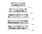
図6は、本発明に係る発光モジュールの製造プロセスの好ましい一実施例を示すフローチャートであり、図に示すように、該製造プロセスは以下のステップを含む。先ず、第1のスルーホール101を有する金属基板1を用意する(ステップS601)、該金属基板1の材質は、例えば、銅またはアルミニウムであり、続いて、第1のスルーホール101を介して搭載ベース5を該金属基板1に配置する(ステップS603)、該搭載ベース5は、例えば、銅の金属材質で、かつ、金または銀のめっき外層を有する。さらに、金属合金21(図3に示すように)を介して共晶溶接方式で該発光ダイオード2を搭載ベース5上にダイボンディングする(ステップS605)。該金属合金21は金及び錫或いは銀及び錫からなり、該搭載ベース5の外層は金または銀がめっきされることにより、金属合金21と共晶溶接する際の接続効果を向上させ、かつより大きな反射率が増加される。また、第2のスルーホール301を有する印刷回路基板3を樹脂のような絶縁コロイド30(図3に示すように)で該金属基板1に貼り付ける(ステップS607)、第2のスルーホール301により搭載ベース5上の発光ダイオード2を印刷回路基板3に露出させ、また、印刷回路基板3は、発光ダイオード2の発光を制御する電気回路(図示せず)を備える。最後に、導電ワイヤ4により、発光ダイオード2を印刷回路基板3にそれぞれ電気的に接続する(ステップS609)。 FIG. 6 is a flowchart showing a preferred embodiment of a manufacturing process of a light emitting module according to the present invention. As shown in the figure, the manufacturing process includes the following steps. First, the
共晶溶接の温度は約280℃であるため、ステップ(S605)までに行った工程及び使用される材料は、ともに高温状態に耐えなければならないため、本発明のプロセスにおいては、高温状態に耐えられない工程或いはそれに使用される材料を利用する工程順番を、共晶溶接の工程の後に調整して行う。 Since the eutectic welding temperature is about 280 ° C., the processes performed up to step (S605) and the materials used must both withstand high temperature conditions. The process order that uses the material that is not used or the material used for it is adjusted after the eutectic welding process.
以下に説明する実施例は、ともに、本発明中の搭載ベース5及び金属基板1の配置方式を述べるものである。 Both of the embodiments described below describe the arrangement of the
図7は、本発明に係る搭載ベース及び金属基板の第1実施例を示す図であり、図に示すように、搭載ベース5及び金属基板1は一体成形され、直接的に金属基板1がミリングされる時に搭載ベース5に成形され、その後、さらに搭載ベース5上に銀または金の外層をめっきする(図示せず)。 FIG. 7 is a view showing a first embodiment of the mounting base and the metal substrate according to the present invention. As shown in the figure, the mounting
図8は、本発明に係る搭載ベース及び金属基板の第2実施例を示す分解図であり、図に示すように、搭載ベース5は第1のスルーホール101を介して金属基板1にかしめされる。 FIG. 8 is an exploded view showing a second embodiment of the mounting base and the metal substrate according to the present invention. As shown in the figure, the mounting
図9は、本発明に係る搭載ベース及び金属基板の第3実施例を示す分解図であり、図に示すように、搭載ベース5はさらにボルト501を凸設し、搭載ベース5は第1のスルーホール101を介して金属基板1にかしめされるとともに、金属基板1の他の側に該ボルト501を露出させ、後段のランプ構造或いは散熱装置等(図示せず)に締め付けることができ、散熱効果を増強させる。 FIG. 9 is an exploded view showing a third embodiment of the mounting base and the metal substrate according to the present invention. As shown in the figure, the mounting
図10は、本発明に係る搭載ベース及び金属基板の第4実施例を示す分解図であり、図に示すように、搭載ベース5自体はねじ態様を有し、第1のスルーホール101を介して金属基板1に締め付ける。 FIG. 10 is an exploded view showing a fourth embodiment of the mounting base and the metal substrate according to the present invention. As shown in the figure, the mounting
以上のように、前記の技術手段により、本発明は金属合金21で共晶溶接を行い、熱を外部の散熱媒介に有効かつ快速的に伝導し、発光ダイオード2自体の温度を低下させる目的を達成できることだけでなく、さらに発光効率及び寿命延長を向上できる。 As described above, by the above technical means, the present invention has the purpose of performing eutectic welding with the
しかし、以上に述べたのは、単に本発明の好ましい具体的な実施例の詳細説明及び図面に過ぎず、本発明の特許請求の範囲を局限するものではなく、本発明の主張する範囲は、下記の特許請求の範囲に基づくべき、いずれの当該分野における通常の知識を有する専門家が本発明の分野の中で、適当に変更や修飾などを実施できるが、それらの実施のことが本発明の主張範囲内に納入されるべきことは言うまでもないことである。 However, what has been described above is merely a detailed description of the preferred specific embodiments and drawings of the present invention, and is not intended to limit the scope of the claims of the present invention. Any expert who has ordinary knowledge in the field, who should be based on the following claims, can appropriately make changes and modifications within the field of the present invention. Needless to say, it should be delivered within the scope of the claim.
従来技術
1金属基板
2発光ダイオード
20銀ペースト
3印刷回路基板
30絶縁コロイド
4導電ワイヤ
5支持ベース
61第1のリードフレーム
62第2のリードフレーム
70絶縁ケース
本発明
1金属基板
101第1のスルーホール
2発光ダイオード
21金属合金
3印刷回路基板
30絶縁コロイド
301第2のスルーホール
4導電ワイヤ
5搭載ベース
501ボルト
Claims (9)
Translated fromJapanese前記金属板体の第1のスルーホールに配置される搭載ベースと、
共晶溶接方式で金属合金を介して前記金属板体に配置された前記搭載ベース上にダイボンディングされる少なくとも一つの発光ダイオードと、
前記搭載ベース上の発光ダイオードを露出させるための第2のスルーホールと、前記少なくとも一つの発光ダイオードの発光を制御する電気回路と、を有し、絶縁コロイドを介して前記金属板体に貼り付けられる印刷回路基板と、
前記発光ダイオードと前記印刷回路基板の前記電気回路とを電気的に接続する少なくとも一本の導電ワイヤと
を含む発光モジュール。And have a first throughhole, the metalplate bodyfabricated of copper material or an aluminum material,
A mounting base disposed in the first through hole of the metalplate ,
At least one light-emitting diode die-bonded on the mounting base disposed on the metalplate through a metal alloy in a eutectic welding method;
A second through hole for exposing the light emitting diode on the mounting base;and an electric circuit for controlling light emission of the at least one light emitting diode, and is attached to the metalplatethrough aninsulating colloid. Printed circuit board,
A light emitting module comprising: the light emitting diode and at least one conductive wire that electrically connects theelectric circuit of the printed circuit board.
ことを特徴とする請求項1記載の発光モジュール。The size of the first through hole corresponds to the size of the mounting base, and the mounting base is made of a copper metal material and has a silver or gold plating outer layer . Light emitting module.
前記搭載ベースが、前記金属板体の第1のスルーホールにかしめられるもの、または、
前記搭載ベースが前記金属板体の第1のスルーホールに螺着されるねじ部を含むもの、
である
ことを特徴とする請求項1記載の発光モジュール。When the metal plate is made of copper, the mounting base is integrated with the metal plate by being formed in the first through hole of the metal plate, or
The mounting base is caulked in the first through hole of the metal plate, or
The mounting base includes a threaded portion that is screwed into the first through hole of the metal plate;
The light emitting module according to claim 1, characterizedin that.
ことを特徴とする請求項3記載の発光モジュール。Claims whereinthe mounting base,when it is caulked to the first through holeof the metalplatemember, characterized in thatthe further projectingly provided a bolt to tighten the heat dissipation apparatus on the other side of the metal plate body Item 4. A light emitting module according to item 3.
ことを特徴とする請求項1記載の発光モジュール。The light emitting module of claim1, wherein saidmetal alloy, characterized inthat made of gold and tin or silver and tin.
ことを特徴とする請求項1記載の発光モジュール。The light emitting module according to claim 1,wherein a main component of the insulating colloid is a resin .
前記第1のスルーホールを介して搭載ベースを前記金属板体に配置するステップと、
共晶溶接方式で少なくとも一つの発光ダイオードを前記金属板体の前記第1のスルーホールに配置された前記搭載ベース上にダイボンディングするステップと、
前記搭載ベース上の前記発光ダイオードを露出させるための第2のスルーホールと、前記少なくとも一つの発光ダイオードの発光を制御する電気回路と、を有する印刷回路基板を、絶縁コロイドを介して前記金属板体に貼り付けるステップと、
少なくとも一本の導電ワイヤを介して前記発光ダイオードを前記印刷回路基板の前記電気回路にそれぞれ電気的に接続するステップと
を含む発光モジュールの製造プロセス。Providing a metal plate body having a first through hole and made of copper or aluminum;
Disposing a mounting base on the metal plate through the first through hole;
Die-bonding at least one light emitting diode on the mounting base disposed in the first through hole of the metal plate by eutectic welding;
A printed circuit board having a second through hole for exposing the light emitting diode on the mounting base and an electric circuit for controlling the light emission of the at least one light emitting diode is formed on the metal plate via an insulating colloid. A step to paste on the body,
Electrically connecting the light emitting diodes to the electrical circuit of the printed circuit board via at least one conductive wire, respectively.
Manufacturing process of light emitting moduleincluding
ことを特徴とする請求項7記載の発光モジュールの製造プロセス。In the eutectic welding method, a metal alloy composed of gold and tin or silver and tin is soldered as a material.
The manufacturing processof the light emitting module accordingto claim 7 .
ことを特徴とする請求項7記載の発光モジュールの製造プロセス。The process for producing a light emitting module according to claim 7, whereina main component of the insulating colloid is a resin .
Applications Claiming Priority (2)
| Application Number | Priority Date | Filing Date | Title |
|---|---|---|---|
| US11/503,216US7494250B2 (en) | 2006-01-26 | 2006-08-14 | Light emitting module and process thereof |
| US11/503,216 | 2006-08-14 |
Publications (2)
| Publication Number | Publication Date |
|---|---|
| JP2008047908A JP2008047908A (en) | 2008-02-28 |
| JP5425381B2true JP5425381B2 (en) | 2014-02-26 |
Family
ID=39181285
Family Applications (1)
| Application Number | Title | Priority Date | Filing Date |
|---|---|---|---|
| JP2007209716AExpired - Fee RelatedJP5425381B2 (en) | 2006-08-14 | 2007-08-10 | Light emitting module and manufacturing process thereof |
Country Status (1)
| Country | Link |
|---|---|
| JP (1) | JP5425381B2 (en) |
Families Citing this family (6)
| Publication number | Priority date | Publication date | Assignee | Title |
|---|---|---|---|---|
| KR101075612B1 (en) | 2009-10-29 | 2011-10-21 | 삼성전기주식회사 | LED package and the method of manufacturing thereof |
| KR101163645B1 (en) | 2009-12-11 | 2012-07-09 | 순천대학교 산학협력단 | High power led module and method for manufacturing the same |
| WO2011123985A1 (en)* | 2010-04-08 | 2011-10-13 | 盈胜科技股份有限公司 | Method for fabricating multilayer light emitting diode array |
| CN102214587B (en)* | 2010-04-08 | 2012-10-17 | 盈胜科技股份有限公司 | Method for making multilayer array type light emitting diode |
| CN102214645B (en)* | 2010-04-08 | 2013-01-09 | 盈胜科技股份有限公司 | Multi-layer Array Type Light Emitting Diodes |
| JP6477734B2 (en)* | 2016-06-30 | 2019-03-06 | 日亜化学工業株式会社 | Light emitting device and manufacturing method thereof |
Family Cites Families (12)
| Publication number | Priority date | Publication date | Assignee | Title |
|---|---|---|---|---|
| JPS63311747A (en)* | 1987-06-15 | 1988-12-20 | Mitsubishi Gas Chem Co Inc | Manufacturing method of printed wiring board for IC chip mounting |
| JPH041738Y2 (en)* | 1987-07-20 | 1992-01-21 | ||
| JP3783572B2 (en)* | 2001-03-05 | 2006-06-07 | 日亜化学工業株式会社 | Light emitting device |
| JP4045781B2 (en)* | 2001-08-28 | 2008-02-13 | 松下電工株式会社 | Light emitting device |
| EP1467414A4 (en)* | 2001-12-29 | 2007-07-11 | Hangzhou Fuyang Xinying Dianzi | A led and led lamp |
| CA2493130A1 (en)* | 2002-07-25 | 2004-02-05 | Jonathan S. Dahm | Method and apparatus for using light emitting diodes for curing |
| JP2004200207A (en)* | 2002-12-16 | 2004-07-15 | Matsushita Electric Works Ltd | Light emitting device |
| JP2004342870A (en)* | 2003-05-16 | 2004-12-02 | Stanley Electric Co Ltd | Light emitting diode for driving large current |
| JP2005064047A (en)* | 2003-08-13 | 2005-03-10 | Citizen Electronics Co Ltd | Light emitting diode |
| JP2005267927A (en)* | 2004-03-17 | 2005-09-29 | Nichia Chem Ind Ltd | Light emitting device |
| JP2005136224A (en)* | 2003-10-30 | 2005-05-26 | Asahi Kasei Electronics Co Ltd | Light emitting diode lighting module |
| JP2005252168A (en)* | 2004-03-08 | 2005-09-15 | Nichia Chem Ind Ltd | Surface mount light emitting device |
- 2007
- 2007-08-10JPJP2007209716Apatent/JP5425381B2/ennot_activeExpired - Fee Related
Also Published As
| Publication number | Publication date |
|---|---|
| JP2008047908A (en) | 2008-02-28 |
Similar Documents
| Publication | Publication Date | Title |
|---|---|---|
| US7494250B2 (en) | Light emitting module and process thereof | |
| US8071998B2 (en) | Light emitting assembly | |
| CA2622775C (en) | Led lighting with integrated heat sink and process for manufacturing same | |
| CN100468795C (en) | Semiconductor light-emitting device integrating heat conduction/radiation module | |
| US7408204B2 (en) | Flip-chip packaging structure for light emitting diode and method thereof | |
| US20080266869A1 (en) | LED module | |
| CN101432899B (en) | Semiconductor light-emitting component, manufacturing method thereof, and semiconductor light-emitting device | |
| JP2003324214A5 (en) | ||
| JP5425381B2 (en) | Light emitting module and manufacturing process thereof | |
| US20070230182A1 (en) | Led module | |
| US7723829B2 (en) | Embedded metal heat sink for semiconductor | |
| CN101307893A (en) | Lighting device | |
| US20110084612A1 (en) | Hybrid chip-on-heatsink device and methods | |
| US20110084303A1 (en) | Radiant heat structure for pin type power led | |
| JP3128955U (en) | Electric circuit board structure with heat dissipation sheet | |
| JP2008233924A (en) | Luminous display panel | |
| JP3938100B2 (en) | LED lamp and LED lighting fixture | |
| KR101028357B1 (en) | LED lighting fixture with heat dissipation | |
| US20050047140A1 (en) | Lighting device composed of a thin light emitting diode module | |
| US20090303685A1 (en) | Interface module with high heat-dissipation | |
| KR101032151B1 (en) | LED lighting modules that attach directly to the heat sink or have their own heat dissipation structure | |
| GB2442074A (en) | Heat sinking LED package | |
| JP2006032804A (en) | Light emitting device and its manufacturing method | |
| JP2011192930A (en) | Substrate, method of manufacturing substrate, and lighting fixture | |
| US7385285B2 (en) | Light assembly |
Legal Events
| Date | Code | Title | Description |
|---|---|---|---|
| A621 | Written request for application examination | Free format text:JAPANESE INTERMEDIATE CODE: A621 Effective date:20100803 | |
| A131 | Notification of reasons for refusal | Free format text:JAPANESE INTERMEDIATE CODE: A131 Effective date:20120522 | |
| A977 | Report on retrieval | Free format text:JAPANESE INTERMEDIATE CODE: A971007 Effective date:20120523 | |
| A601 | Written request for extension of time | Free format text:JAPANESE INTERMEDIATE CODE: A601 Effective date:20120821 | |
| A602 | Written permission of extension of time | Free format text:JAPANESE INTERMEDIATE CODE: A602 Effective date:20120824 | |
| A521 | Written amendment | Free format text:JAPANESE INTERMEDIATE CODE: A523 Effective date:20120827 | |
| A131 | Notification of reasons for refusal | Free format text:JAPANESE INTERMEDIATE CODE: A131 Effective date:20120918 | |
| A521 | Written amendment | Free format text:JAPANESE INTERMEDIATE CODE: A523 Effective date:20121217 | |
| A02 | Decision of refusal | Free format text:JAPANESE INTERMEDIATE CODE: A02 Effective date:20130507 | |
| A521 | Written amendment | Free format text:JAPANESE INTERMEDIATE CODE: A523 Effective date:20130905 | |
| A521 | Written amendment | Free format text:JAPANESE INTERMEDIATE CODE: A821 Effective date:20130905 | |
| A911 | Transfer of reconsideration by examiner before appeal (zenchi) | Free format text:JAPANESE INTERMEDIATE CODE: A911 Effective date:20130930 | |
| TRDD | Decision of grant or rejection written | ||
| A01 | Written decision to grant a patent or to grant a registration (utility model) | Free format text:JAPANESE INTERMEDIATE CODE: A01 Effective date:20131105 | |
| A61 | First payment of annual fees (during grant procedure) | Free format text:JAPANESE INTERMEDIATE CODE: A61 Effective date:20131127 | |
| R150 | Certificate of patent or registration of utility model | Free format text:JAPANESE INTERMEDIATE CODE: R150 | |
| LAPS | Cancellation because of no payment of annual fees |