JP5421551B2 - Plasma processing apparatus and plasma processing method - Google Patents
Plasma processing apparatus and plasma processing methodDownload PDFInfo
- Publication number
- JP5421551B2 JP5421551B2JP2008153423AJP2008153423AJP5421551B2JP 5421551 B2JP5421551 B2JP 5421551B2JP 2008153423 AJP2008153423 AJP 2008153423AJP 2008153423 AJP2008153423 AJP 2008153423AJP 5421551 B2JP5421551 B2JP 5421551B2
- Authority
- JP
- Japan
- Prior art keywords
- coaxial waveguide
- inner conductor
- conductor
- coaxial
- plasma processing
- Prior art date
- Legal status (The legal status is an assumption and is not a legal conclusion. Google has not performed a legal analysis and makes no representation as to the accuracy of the status listed.)
- Active
Links
Images


Classifications
- H—ELECTRICITY
- H01—ELECTRIC ELEMENTS
- H01J—ELECTRIC DISCHARGE TUBES OR DISCHARGE LAMPS
- H01J37/00—Discharge tubes with provision for introducing objects or material to be exposed to the discharge, e.g. for the purpose of examination or processing thereof
- H01J37/32—Gas-filled discharge tubes
- H01J37/32009—Arrangements for generation of plasma specially adapted for examination or treatment of objects, e.g. plasma sources
- H01J37/32192—Microwave generated discharge
- H01J37/32211—Means for coupling power to the plasma
- H—ELECTRICITY
- H01—ELECTRIC ELEMENTS
- H01J—ELECTRIC DISCHARGE TUBES OR DISCHARGE LAMPS
- H01J37/00—Discharge tubes with provision for introducing objects or material to be exposed to the discharge, e.g. for the purpose of examination or processing thereof
- H01J37/32—Gas-filled discharge tubes
- H01J37/32009—Arrangements for generation of plasma specially adapted for examination or treatment of objects, e.g. plasma sources
- H01J37/32192—Microwave generated discharge
- H01J37/32211—Means for coupling power to the plasma
- H01J37/32229—Waveguides
Landscapes
- Physics & Mathematics (AREA)
- Engineering & Computer Science (AREA)
- Plasma & Fusion (AREA)
- Chemical & Material Sciences (AREA)
- Analytical Chemistry (AREA)
- Plasma Technology (AREA)
Description
Translated fromJapanese本発明は、電磁波を用いてプラズマを生成し、被処理体上にプラズマ処理を施すプラズマ処理装置及びプラズマ処理方法に関する。特に、伝送路のインピーダンス整合に関する。 The present invention relates to a plasma processing apparatus and a plasma processing method for generating plasma using electromagnetic waves and performing plasma processing on an object to be processed. In particular, it relates to impedance matching of transmission lines.
マイクロ波プラズマ処理装置では、ガスを励起させてプラズマを生成するために、ガスを電離や解離させるためのエネルギーとして所望のマイクロ波を伝送路に伝送させ、処理容器内に放出する。処理容器の天井面にガスの通り道を設け、天井面をシャワープレートにして天井面から処理容器内にガスを導入する構成のプラズマ処理装置では、マイクロ波を伝送させる同軸管等と干渉しない位置にガス流路を設けなければならないため、同軸管の太さをあまり太くすることができない。 In the microwave plasma processing apparatus, in order to generate plasma by exciting a gas, a desired microwave is transmitted to a transmission path as energy for ionizing or dissociating the gas and is released into a processing container. In a plasma processing apparatus configured to provide gas passages on the ceiling surface of the processing vessel and to introduce gas from the ceiling surface into the processing vessel using the ceiling surface as a shower plate, it is at a position that does not interfere with a coaxial tube that transmits microwaves. Since the gas flow path must be provided, the thickness of the coaxial tube cannot be increased too much.
一方、均一なプラズマを安定的に生成するためにはかなりの電力が必要である。たとえば、高密度プラズマを励起するには同軸管に数100W〜数kWのマイクロ波を伝送させなければならないので、同軸管の内部導体の電流密度が大きくなり、加熱されてしまう問題がある。同軸管の内部導体が加熱されると、内部導体を保持しているテフロン(登録商標)リング等が変形、変質したり、内部導体表面が酸化されたり、内部導体が延びて各部にストレスがかかり破損してしまう危険性がある。 On the other hand, considerable power is required to stably generate a uniform plasma. For example, in order to excite high-density plasma, microwaves of several hundred watts to several kWs must be transmitted to the coaxial tube, which causes a problem that the current density of the inner conductor of the coaxial tube is increased and heated. When the inner conductor of the coaxial tube is heated, the Teflon (registered trademark) ring holding the inner conductor is deformed and altered, the inner conductor surface is oxidized, the inner conductor is extended, and stress is applied to each part. There is a risk of damage.
同軸管の破損を避けながら大電力のマイクロ波をプラズマに供給するためには、同軸管の特性インピーダンスを各部でそれぞれ最適化してマイクロ波の反射を最小限に抑える必要がある。ところが、従来のプラズマ処理装置では、構造が単純な同じ太さの同軸管を用いてマイクロ波を処理容器内に供給していた(たとえば、特許文献1を参照)。このため、特性インピーダンスは、同軸管の長手方向に沿って一様であった。 In order to supply a high-power microwave to the plasma while avoiding damage to the coaxial tube, it is necessary to optimize the characteristic impedance of the coaxial tube in each part to minimize the reflection of the microwave. However, in the conventional plasma processing apparatus, a microwave is supplied into the processing container using a coaxial tube having the same thickness and having a simple structure (see, for example, Patent Document 1). For this reason, the characteristic impedance is uniform along the longitudinal direction of the coaxial waveguide.
しかしながら、処理容器の天井面に設けられ、同軸管を伝送したマイクロ波を処理容器内に放出するための誘電体板を薄くすると、プラズマの均一性は高くなるものの、プラズマ側からのマイクロ波の反射を小さくするためには、誘電体板に隣接した同軸管の出力側(同軸管のプラズマ側の端部)の特性インピーダンスを10〜20Ω程度に抑える必要が生じる。これに対して、高い電力を供給するためには、誘電体板に隣接した同軸管の入力側(同軸管のマイクロ波源側の端部)の特性インピーダンスは、10〜20Ωより大きくする必要がある。よって、従来のように長手方向に沿って特性インピーダンスが一様な同じ太さの同軸管では、プラズマ側からのマイクロ波の反射が大きく、大きな電力を伝送させることができなかった。 However, if the dielectric plate that is provided on the ceiling surface of the processing vessel and releases the microwave transmitted through the coaxial tube into the processing vessel is thin, the uniformity of the plasma is increased, but the microwave from the plasma side is increased. In order to reduce the reflection, it is necessary to suppress the characteristic impedance on the output side of the coaxial tube adjacent to the dielectric plate (the end portion on the plasma side of the coaxial tube) to about 10 to 20Ω. On the other hand, in order to supply high power, the characteristic impedance on the input side of the coaxial tube adjacent to the dielectric plate (the end of the coaxial tube on the microwave source side) needs to be larger than 10 to 20Ω. . Therefore, in the conventional coaxial tube having the same thickness and uniform characteristic impedance along the longitudinal direction as in the prior art, the reflection of the microwave from the plasma side is large, and a large amount of power cannot be transmitted.
上記課題を解消するために、本発明は、特性インピーダンスが入力側と出力側で異なる同軸管構造を有するプラズマ処理装置を提供する。 In order to solve the above problems, the present invention provides a plasma processing apparatus having a coaxial tube structure having different characteristic impedances on the input side and the output side.
すなわち、上記課題を解決するために、本発明のある態様によれば、電磁波によりガスを励起させて被処理体をプラズマ処理するプラズマ処理装置であって、処理容器と、電磁波を出力する電磁波源と、内部導体の外径と外部導体の内径との比が入力側から出力側に向かう方向に沿って一様でない構造を有し、前記電磁波源から出力された電磁波を伝送させる第1の同軸管と、前記処理容器の内部に面しかつ前記第1の同軸管に隣接し、前記第1の同軸管を伝送した電磁波を前記処理容器の内部に放出する誘電体板と、を備え、前記第1の同軸管の外部導体の内径は、入力側と出力側とで実質的に等しく、かつ、入力側から出力側までの間の部分も段差なしで実質的に等しく、前記第1の同軸管の内部導体の入力側の外径は、前記第1の同軸管の内部導体の出力側の外径より小さく、前記第1の同軸管の内部導体の外径と外部導体の内径との比は、前記第1の同軸管の電磁波の入力側の特性インピーダンスが前記第1の同軸管の電磁波の出力側の特性インピーダンスよりも大きくなるように定められているプラズマ処理装置が提供される。That is, in order to solve the above-described problem, according to an aspect of the present invention, there is provided a plasma processing apparatus that plasmas a target object by exciting a gas with an electromagnetic wave, the processing container, and an electromagnetic wave source that outputs the electromagnetic wave And the ratio between the outer diameter of the inner conductor and the inner diameter of the outer conductor is not uniform along the direction from the input side to the output side, and a first coaxial for transmitting the electromagnetic wave output from the electromagnetic wave source comprising a tube, adjacent to the coaxial waveguide and the first facing the interior of the processing container, and a dielectric plate that emits the interior of the first coaxial waveguide the processing vessel electromagnetic waves transmitting thesaid The inner diameter of the outer conductor of the first coaxial tube is substantially equal on the input side and the output side, and the portion between the input side and the output side is also substantially equal without a step, and the first coaxial tube The outer diameter on the input side of the inner conductor of the tube is the first coaxial Of smaller than the outer diameter of the output side of the inner conductor, the ratio between the outer diameter and the outer conductor inner diameter of the first inner conductor of the coaxial waveguide, the characteristic impedance of the input side of the electromagnetic waves of the first coaxial tubes wherein A plasma processing apparatus is provided which is determined to be larger than the characteristic impedance on the output side of the electromagnetic wave of the first coaxial waveguide.
同軸管の特性インピーダンスは、同軸管の内部導体の外径と外部導体の内径との比の変化によって変化する。よって、内部導体の外径と外部導体の内径との比が長手方向に沿って一様でない第1の同軸管の構造によれば、第1の同軸管の特性インピーダンスは長手方向に沿って一様でなくなる。これにより、第1の同軸管の入力側の特性インピーダンスと第1の同軸管の出力側の特性インピーダンスとを異ならせることができる。そして、入力側の特性インピーダンスを出力側の特性インピーダンスよりも大きくすることにより、プラズマ側からの電磁波の反射を小さく抑えるとともに、同軸管に大きな電力を伝送させることができる。The characteristic impedance of the coaxial waveguide is changed by a change in the ratio between theouter diameter and the outer conductorinner diameter ofthe inner conductor of the coaxial tube. Therefore, according to the structure of the first coaxial waveguidein which the ratio betweenthe outer diameterof the inner conductor andthe innerdiameter of the outer conductor is not uniform along the longitudinal direction, the characteristic impedance of the first coaxial waveguide is constant along the longitudinal direction. It will not be like. Thereby, the characteristic impedance on the input side of the first coaxial waveguide and the characteristic impedance on the output side of the first coaxial waveguide can be made different.By making the characteristic impedance on the input side larger than the characteristic impedance on the output side, reflection of electromagnetic waves from the plasma side can be suppressed to a small level, and a large amount of power can be transmitted to the coaxial waveguide.
内部導体の外径と外部導体の内径との比が長手方向に沿って一様でない第1の同軸管の構造としては、たとえば、前記第1の同軸管の外部導体の内径が入力側と出力側とで実質的に等しく、前記第1の同軸管の内部導体の入力側の外径が、前記第1の同軸管の内部導体の出力側の外径より小さい場合が挙げられる。その場合、前記第1の同軸管の内部導体の外径を前記入力側から前記出力側に向かって連続的に大きくしてもよい。As the structure of the first coaxial waveguidein which the ratio betweenthe outer diameterof the inner conductor andthe innerdiameter of the outer conductor is not uniform along the longitudinal direction, for example,the inner diameter of the outer conductor of the first coaxial waveguide is the input side and the output side. And theouter diameter of the input side of the inner conductor of the first coaxial waveguideis smaller than theouter diameter of the output side of the inner conductor of the first coaxial waveguide. In that case, it may be continuouslyincreasingthe outer diameter of the inner conductor of the first coaxial waveguide toward theentering-force side to the output side.
前記第1の同軸管の外部導体の入力側の内径を前記第1の同軸管の外部導体の出力側の内径より大きくしてもよい。その場合、前記第1の同軸管の外部導体の内径を前記入力側から前記出力側に向かって連続的に小さくしてもよい。また、前記第1の同軸管の内部導体の外径を入力側と出力側とで実質的に等しくてもよい。さらに、前記第1の同軸管の内部導体及び外部導体の少なくともいずれかに段差部を設けることにより、前記第1の同軸管の内部導体の外径と外部導体の内径との比を不連続に変化させてもよい。Theinner diameter on the input side of the outer conductor of the first coaxial waveguide may belarger than theinner diameter on the output side of the outer conductor of the first coaxial waveguide. In that case, may be continuouslyreduced inner diameter of the outer conductor of the first coaxial waveguide toward theentering-force side to the output side.The outer diameter of the inner conductor of the first coaxial waveguide may be substantially equal on the input side and the output side. Further, by providing a step portion in at least one of the inner conductor and the outer conductor of the first coaxial waveguide,the ratioof the outer diameter of the inner conductorof the first coaxial waveguide tothe innerdiameter of the outer conductor is made discontinuous. It may be changed.
図12に示したように、第1の同軸管の入力側の特性インピーダンスが18Ω〜46Ωになるように第1の同軸管の形状を最適化することにより、細い同軸管でも大きな電力を供給することができる。図12によれば、第1の同軸管の入力側の特性インピーダンスを22Ω〜40Ωに限定すれば、さらに大きな電力を供給することができ、好ましい。 As shown in FIG. 12, by optimizing the shape of the first coaxial tube so that the characteristic impedance on the input side of the first coaxial tube is 18Ω to 46Ω, large power is supplied even to a thin coaxial tube. be able to. According to FIG. 12, if the characteristic impedance on the input side of the first coaxial waveguide is limited to 22Ω to 40Ω, it is possible to supply a larger electric power, which is preferable.
前記第1の同軸管の内部導体は、部分的に細くなったくびれ部を有していてもよい。これは、第1の同軸管に直列にインダクタンスを挿入したことと等価であり、くびれ部の直径や長さにより挿入されるインダクタンスの値を最適化することにより、反射を抑えることが可能になる。 The inner conductor of the first coaxial waveguide may have a constricted portion that is partially narrowed. This is equivalent to inserting an inductance in series with the first coaxial waveguide, and it is possible to suppress reflection by optimizing the value of the inductance inserted depending on the diameter and length of the constricted portion. .
また、前記第1の同軸管の内部導体と外部導体との間には、前記誘電体板に隣接して誘電体リングが設けられていてもよい。これは、第1の同軸管と並列にキャパシタンスを挿入したことと等価であり、誘電体リングの厚さや誘電率により挿入されるキャパシタンスの値を最適化することにより、反射を抑えることが可能になる。また、誘電体リングにより誘電体板近傍の隙間を埋めることにより、第1の同軸管と誘電体板との隣接部分に電界が集中することを避け、異常放電を防止することができる。 A dielectric ring may be provided adjacent to the dielectric plate between the inner conductor and the outer conductor of the first coaxial waveguide. This is equivalent to inserting a capacitance in parallel with the first coaxial waveguide, and it is possible to suppress reflection by optimizing the value of the inserted capacitance depending on the thickness of the dielectric ring and the dielectric constant. Become. In addition, by filling the gap in the vicinity of the dielectric plate with the dielectric ring, it is possible to prevent the electric field from concentrating on the adjacent portion between the first coaxial waveguide and the dielectric plate, and to prevent abnormal discharge.
前記第1の同軸管の内部導体と外部導体との間には、第1の誘電体支持部材が設けられ、前記第1の誘電体支持部材は、前記第1の同軸管の内部導体の外周に形成された溝に嵌入されていてもよい。第1の同軸管の内部導体を外部導体に支持するためである。さらに、第1の同軸管と並列にキャパシタンスを挿入したことと等価であり、誘電体リングの厚さや誘電率により挿入されるキャパシタンスの値を最適化することにより、反射を抑えることが可能になる。 A first dielectric support member is provided between the inner conductor and the outer conductor of the first coaxial waveguide, and the first dielectric support member is an outer periphery of the inner conductor of the first coaxial waveguide. It may be inserted into the groove formed in the. This is because the inner conductor of the first coaxial waveguide is supported by the outer conductor. Furthermore, this is equivalent to inserting a capacitance in parallel with the first coaxial waveguide, and it is possible to suppress reflection by optimizing the value of the inserted capacitance depending on the thickness of the dielectric ring and the dielectric constant. .
前記第1の同軸管に連結され、前記第1の同軸管に電磁波を伝送する第2の同軸管と、前記第1の同軸管の内部導体と前記第2の同軸管の内部導体との連結部に設けられ、前記第1の同軸管の内部導体を直接的にまたは他の部材を介して間接的に前記誘電体板に押し付けるバネ部材を有していてもよい。これによれば、バネ部材の弾性力により第1の同軸管の内部導体を直接的にまたは他の部材を介して間接的に誘電体板側に押しつけて密着させることによって電磁波の伝送を安定化させることができる。 A second coaxial waveguide connected to the first coaxial waveguide and transmitting electromagnetic waves to the first coaxial waveguide, and a connection between an inner conductor of the first coaxial waveguide and an inner conductor of the second coaxial waveguide. There may be provided a spring member that is provided in the portion and presses the inner conductor of the first coaxial waveguide directly or indirectly to the dielectric plate via another member. According to this, transmission of electromagnetic waves is stabilized by pressing the inner conductor of the first coaxial waveguide directly or indirectly to the dielectric plate side through another member by the elastic force of the spring member. Can be made.
前記第1の同軸管の内部導体と前記第2の同軸管の内部導体との連結部には、前記第1の同軸管の内部導体と前記第2の同軸管の内部導体とを電気的に接続する接点部材を設けてもよい。 The connecting portion between the inner conductor of the first coaxial waveguide and the inner conductor of the second coaxial waveguide electrically connects the inner conductor of the first coaxial waveguide and the inner conductor of the second coaxial waveguide. You may provide the contact member to connect.
前記第2の同軸管の内部導体は、前記第1の同軸管の内部導体よりも太くなっていてもよい。前記連結部には、前記第2の同軸管の内部導体に対して前記第1の同軸管の内部導体の角度が変えられる遊びがあってもよい。装置の組み立てを容易にするためである。 The inner conductor of the second coaxial waveguide may be thicker than the inner conductor of the first coaxial waveguide. The connecting portion may have a play in which an angle of the inner conductor of the first coaxial waveguide is changed with respect to the inner conductor of the second coaxial waveguide. This is to facilitate the assembly of the device.
前記第2の同軸管の内部導体と外部導体との間には、第2の誘電体支持部材が設けられ、前記第2の誘電体支持部材は、前記第2の同軸管の内部導体の外周に形成された溝に嵌入されていてもよい。第2の同軸管の内部導体を外部導体に支持するためである。 A second dielectric support member is provided between the inner conductor and the outer conductor of the second coaxial waveguide, and the second dielectric support member is an outer periphery of the inner conductor of the second coaxial waveguide. It may be inserted into the groove formed in the. This is because the inner conductor of the second coaxial waveguide is supported by the outer conductor.
前記連結部近傍の前記第2の同軸管の内部導体と外部導体との間には、誘電体ロッドが設けられ、前記誘電体ロッドは、前記第2の同軸管の内部導体に設けられた穴に嵌入されていてもよい。第2の同軸管の内部導体を外部導体に支持するためである。 A dielectric rod is provided between the inner conductor and the outer conductor of the second coaxial waveguide in the vicinity of the connecting portion, and the dielectric rod is a hole provided in the inner conductor of the second coaxial waveguide. It may be inserted in. This is because the inner conductor of the second coaxial waveguide is supported by the outer conductor.
前記連結部には、前記第1の同軸管の内部導体が前記第2の同軸管の内部導体から脱落することを防止するための係合部が形成されていてもよい。 An engaging portion for preventing the inner conductor of the first coaxial waveguide from dropping from the inner conductor of the second coaxial waveguide may be formed in the connecting portion.
前記第1の同軸管の内部導体と前記誘電体板との間は、金属金具を介して隣接していてもよい。これによれば、金属金具により第1の同軸管の内部導体と前記誘電体板との密着性を高め、電磁波の伝送が乱れることを防止することができる。 The inner conductor of the first coaxial waveguide and the dielectric plate may be adjacent to each other via a metal fitting. According to this, it is possible to improve the adhesion between the inner conductor of the first coaxial waveguide and the dielectric plate by the metal fitting, and to prevent the transmission of electromagnetic waves from being disturbed.
前記連結部における前記第1の同軸管の特性インピーダンスと前記第2の同軸管の特性インピーダンスとは等しくなっていてもよい。連結部を伝送する電磁波の反射を抑えるためである。 The characteristic impedance of the first coaxial waveguide and the characteristic impedance of the second coaxial waveguide in the connecting portion may be equal. This is to suppress reflection of electromagnetic waves transmitted through the connecting portion.
上記課題を解決するために、本発明の他の態様によれば、処理容器の内部にガスを導入し、電磁波源から電磁波を出力し、電磁波の入力側の特性インピーダンスが出力側の特性インピーダンスよりも大きくなるように、内部導体の外径と外部導体の内径との比が入力側から出力側に向かう方向に沿って一様でない構造を有する第1の同軸管に前記出力した電磁波を伝送し、前記第1の同軸管の外部導体の内径は、入力側と出力側とで実質的に等しく、かつ、入力側から出力側までの間の部分も段差なしで実質的に等しく、前記第1の同軸管の内部導体の入力側の外径は、前記第1の同軸管の内部導体の出力側の外径より小さく、前記第1の同軸管を伝送した電磁波を、前記処理容器の内部に面しかつ前記第1の同軸管に隣接した誘電体板から前記処理容器の内部に放出し、前記放出された電磁波により前記導入されたガスを励起させて被処理体をプラズマ処理するプラズマ処理方法が提供される。In order to solve the above-described problem, according to another aspect of the present invention, gas is introduced into the processing container, electromagnetic waves are output from the electromagnetic wave source, and the characteristic impedance on the input side of the electromagnetic waves is more than the characteristic impedance on the output side. So that the ratio between the outer diameter of the inner conductor and the inner diameter of the outer conductor is not uniform along the direction from the input side to the output side.The inner diameter of the outer conductor of the first coaxial waveguide is substantially equal between the input side and the output side, and the portion between the input side and the output side is also substantially equal without a step, The outer diameter on the input side of the inner conductor of the first coaxial pipe is smaller than the outer diameter on the output side of the inner conductor of the first coaxial pipe, and the electromagnetic wave transmitted through the first coaxial pipeis introduced into the processing container. From a dielectric plate facing and adjacent to the first coaxial waveguide Released into the interior of the serial processing container, plasma processing method wherein the emitted electromagnetic waves by exciting the introduced gas plasma processing a workpiece with are provided.
これによれば、特性インピーダンスが長手方向に沿って一様でない構造の第1の同軸管を用いて、プラズマ側からの電磁波の反射を小さく抑えるとともに、同軸管に大きな電力を伝送させることができる。 According to this, it is possible to suppress the reflection of electromagnetic waves from the plasma side to be small and to transmit large electric power to the coaxial tube by using the first coaxial tube whose characteristic impedance is not uniform along the longitudinal direction. .
以上に説明したように、本発明によれば、同軸管の入力側と出力側で特性インピーダンスを異ならせることができる。 As described above, according to the present invention, the characteristic impedance can be made different between the input side and the output side of the coaxial waveguide.
以下に添付図面を参照しながら、本発明の好適な実施形態について詳細に説明する。なお、以下の説明及び添付図面において、同一の構成及び機能を有する構成要素については、同一符号を付することにより、重複説明を省略する。 Hereinafter, preferred embodiments of the present invention will be described in detail with reference to the accompanying drawings. In the following description and the accompanying drawings, the same reference numerals are given to the constituent elements having the same configuration and function, and redundant description is omitted.
(第1実施形態)
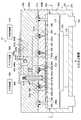
まず、本発明の第1実施形態にかかるマイクロ波プラズマ処理装置の構成について、図1及び図2を参照しながら説明する。図1は、本実施形態に係るマイクロ波プラズマ処理装置10の縦断面である。図1は、図2の2−O−O’−2断面を示している。図2は、本装置10の天井面であり、図1の1−1断面を示している。(First embodiment)
First, the configuration of the microwave plasma processing apparatus according to the first embodiment of the present invention will be described with reference to FIGS. 1 and 2. FIG. 1 is a longitudinal section of a microwave
(マイクロ波プラズマ処理装置の概略)
図2に示したように、マイクロ波プラズマ処理装置10は、ガラス基板(以下、「基板G」という。)をプラズマ処理するための処理容器100を有している。処理容器100は、容器本体200と蓋体300とから構成される。容器本体200は、その上部が開口された有底立方体形状を有していて、その開口は蓋体300により閉塞されている。蓋体300は、上部蓋体300aと下部蓋体300bとから構成されている。容器本体200と下部蓋体300bとの接触面にはOリング205が設けられていて、これにより容器本体200と下部蓋体300bとが密閉され、処理室が画定される。上部蓋体300aと下部蓋体300bとの接触面にもOリング210及びOリング215が設けられていて、これにより、上部蓋体300aと下部蓋体300bとが密閉されている。容器本体200及び蓋体300は、たとえば、アルミニウム合金等の金属からなり、電気的に接地されている。(Outline of microwave plasma processing equipment)
As shown in FIG. 2, the microwave
処理容器100の内部には、基板Gを載置するためのサセプタ105(ステージ)が設けられている。サセプタ105は、たとえば窒化アルミニウムから形成されている。サセプタ105は、支持体110に支持されていて、その周囲には処理室のガスの流れを好ましい状態に制御するためのバッフル板115が設けられている。また、処理容器100の底部にはガス排出管120が設けられていて、処理容器100の外部に設けられた真空ポンプ(図示せず)を用いて処理容器100内のガスが排出される。 A susceptor 105 (stage) for placing the substrate G is provided inside the
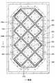
図1及び図2を見ると、処理容器100の天井面には、誘電体板305、金属電極310及び金属カバー320が規則的に配置されている。金属電極310及び金属カバー320の周囲には、サイドカバー350が設けられている。誘電体板305、金属電極310及び金属カバー320は、僅かに角が削られた略正方形のプレートである。なお、菱形であってもよい。本明細書において、金属電極310は、金属電極310の外縁部から誘電体板305が概ね均等に露出するように誘電体板305に隣接して設けられた平板をいう。これにより、誘電体板305は、蓋体300の内壁と金属電極310によりサンドイッチされる。金属電極310は、処理容器100の内壁と電気的に接続されている。 1 and 2, the
誘電体板305及び金属電極310は、基板Gや処理容器100に対して概ね45°傾いた位置に等ピッチで8枚配置される。ピッチは、一つの誘電体板305の対角線の長さが、隣り合う誘電体板305の中心間の距離の0.9倍以上になるように定められている。これにより、誘電体板305のわずかに削られた角部同士は隣接して配置される。 The eight
金属電極310と金属カバー320は、誘電体板320の厚さ分、金属カバー320の方が厚い。かかる形状によれば、天井面の高さがほぼ等しくなると同時に、誘電体板305が露出した部分やその近傍の凹みの形状もすべてほぼ同じパターンになる。 The
誘電体板305はアルミナにより形成され、金属電極310、金属カバー320及びサイドカバー350はアルミニウム合金により形成されている。なお、本実施形態では、8枚の誘電体板305及び金属電極310が2列に4段配置されるが、これに限られず、誘電体板305及び金属電極310の枚数を増やすことも減らすこともできる。 The
誘電体板305及び金属電極310は、ねじ325により4カ所から均等に支持されている(図2参照)。図1に示したように、上部蓋体300aと下部蓋体300bとの間には、紙面に垂直な方向に格子状に形成された主ガス流路330が設けられている。主ガス流路330は、複数のねじ325内に設けられたガス流路325aにガスを分流する。ガス流路325aの入口には、流路を狭める細管335が嵌入されている。細管335は、セラミックスや金属からなる。金属電極310と誘電体板305との間にはガス流路310aが設けられている。金属カバー320と誘電体板305との間及びサイドカバー350と誘電体板305との間にもガス流路320aが設けられている。ねじ325の先端面は、プラズマの分布を乱さないように、金属電極310、金属カバー320及びサイドカバー350の下面と面一になっている。金属電極310に開口されたガス放出穴345aと金属カバー320やサイドカバー350に開口されたガス放出穴345bとは均等なピッチで配設されている。 The
ガス供給源905から出力されたガスは、主ガス流路330からガス流路325a(枝ガス流路)を通過し、金属電極310内の第1のガス流路310a及び金属カバー320やサイドカバー350内の第2のガス流路320aを通ってガス放出穴345a、345bから処理室内に供給される。第1の同軸管610の外周近傍の下部蓋体300bと誘電体板305との接触面にはOリング220が設けられていて、第1の同軸管610内の大気が処理容器100の内部に入らないようになっている。 The gas output from the
このようにして天井部の金属面にガスシャワープレートを形成することにより、従来生じていた、プラズマ中のイオンによる誘電体板表面のエッチング及び処理容器内壁への反応生成物の堆積を抑制し、コンタミやパーティクルの低減を図ることができる。また、誘電体と異なり金属は加工が容易であるため、コストを大幅に低減することができる。 In this way, by forming the gas shower plate on the metal surface of the ceiling portion, it has been possible to suppress the etching of the dielectric plate surface caused by ions in the plasma and the deposition of reaction products on the inner wall of the processing vessel, It is possible to reduce contamination and particles. Further, unlike a dielectric, a metal can be easily processed, so that the cost can be greatly reduced.
蓋体300を掘り込んで形成された第1の同軸管の外部導体610bには、内部導体610aが挿入されている。同様にして掘り込んで形成された第2〜第4の同軸管の外部導体620b〜640bには、第2〜第4の同軸管の内部導体620a〜640aが挿入され、その上部は蓋体カバー660で覆われている。各同軸管の内部導体は熱伝導のよい銅で形成されている。 An
図1に示した誘電体板305の表面は、第1の同軸管610から誘電体板305にマイクロ波が入射する部分と誘電体板305からマイクロ波が放出される部分を除いて金属膜305aにて被覆されている。これにより、誘電体板305とそれに隣接する部材間に生じた空隙によってもマイクロ波の伝搬が乱されず、安定してマイクロ波を処理容器内に導くことができる。 The surface of the
図2に示したように、誘電体板305は、誘電体板305に一対一に隣接した金属電極310と誘電体板305が配置されていない処理容器100の内壁(金属カバー320で覆われた処理容器100の内壁を含む)の間から露出している。誘電体板305と誘電体板305が配置されていない処理容器100の内壁(金属カバー320で覆われた処理容器100の内壁を含む)とは、実質的に相似をなす形状か、または実質的に対称となる形状となっている。これにより、誘電体板から金属電極側及び内壁側(金属カバー320及びサイドカバー350側)に概ね均等にマイクロ波の電力を供給することができる。この結果、誘電体板305から放出されたマイクロ波は、表面波となって電力を半分に分配しながら金属電極310、金属カバー320及びサイドカバー350の表面を伝搬する。処理容器内面の金属面とプラズマとの間を伝搬する表面波を、以下、導体表面波(金属表面波:Metal Surface Wave)という。これにより、天井面全体に、導体表面波が伝搬し、本実施形態に係るマイクロ波プラズマ処理装置10の天井面下方にて、均一なプラズマが安定的に生成される。 As shown in FIG. 2, the
サイドカバー350には、8枚の誘電体板305の全体を囲むように8角形の溝340が形成されていて、天井面を伝搬する導体表面波が、溝340より外側に伝搬することを抑制する。複数の溝340を平行に多重に形成してもよい。 The
一枚の金属電極310を中心として、隣接する金属カバー320の中心点を頂点に持つ領域を、以下、セルCel(図1参照)という。天井面では、セルCelを一単位として同一パターンの構成が8セルCel規則正しく配置されている。 A region having the center point of the
冷媒供給源910は、蓋体内部の冷媒配管910a及び第4の同軸管の内部導体640aの冷媒配管910bに接続されていて、冷媒供給源910から供給された冷媒が冷媒配管910a、910b内を循環して再び冷媒供給源910に戻ることにより、蓋体300及び内部導体の加熱を抑止するようになっている。 The refrigerant supply source 910 is connected to the
(同軸管内部導体固定)
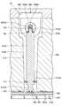
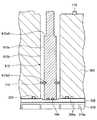
次に、第1及び第2の同軸管及びその連結部分について、図3〜図5を参照しながら説明する。図3は、第1及び第2の同軸管610、620及びその連結部分Dcの断面図である。図4は、図3の3−3断面である。図5は、図3の4−4断面である。(Fixed inner conductor of coaxial tube)
Next, the first and second coaxial waveguides and their connecting portions will be described with reference to FIGS. FIG. 3 is a cross-sectional view of the first and second
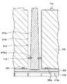
前述したように、第1の同軸管610は、内部導体610a及び外部導体610bから形成されている。同様に、第2の同軸管620は、内部導体620a及び外部導体620bから形成されている。第1及び第2の同軸管610、620の内部導体は、いずれも銅で形成されている。外部導体610b、620bは、蓋体300に形成された掘り込みと蓋体カバー660により画定されている。第1の同軸管610と第2の同軸管620とは、連結部Dcにて概ね垂直に連結されている。 As described above, the first
連結部Dcでは、第2の同軸管の下面に形成された有底の縦穴620a1に、第1の同軸管の内部導体610aの先端に形成されたロッド610a1が嵌め込まれている。 In the connecting portion Dc, a rod 610a1 formed at the tip of the
第1の同軸管の内部導体610aの外周に形成された溝610a2には、誘電体リング710(第1の誘電体支持部材の一例)が嵌入され、これにより、内部導体610aを外部導体610bに支持して内部導体610aの軸ぶれを防止するようになっている。 A dielectric ring 710 (an example of a first dielectric support member) is fitted into a groove 610a2 formed on the outer periphery of the
第2の同軸管の内部導体620aの外周に形成された溝620a2にも、誘電体リング715(第2の誘電体支持部材の一例)が嵌入され、これにより、内部導体620aを外部導体620bに支持するようになっている。誘電体リング710、715は、たとえば、テフロンにより形成されている。 A dielectric ring 715 (an example of a second dielectric support member) is also inserted into a groove 620a2 formed on the outer periphery of the
第2の同軸管の内部導体620aは、誘電体ロッド720によって側部からも支持されている。誘電体ロッド720は、第2の同軸管の内部導体620aに設けられた有底の横穴620a3に挿入され、ロッド610a1に設けられた横穴を貫通して、横穴620a3の底部まで嵌入される。 The
このようにして、第1の同軸管の内部導体610aは、誘電体ロッド720により第2の同軸管620の内部導体620aに固定される。かかる構成によれば、装置を組み立てる際に、第1の同軸管の内部導体610aと第2の同軸管の内部導体620aとが連結された状態で蓋体300に形成された掘り込みに嵌め込むことができるため、施工しやすい。また、ねじを用いずに第1及び第2の同軸管の内部導体610a,620aを連結及び固定し、第1の同軸管の内部導体610aが第2の同軸管の内部導体620aから脱落することを防止できる。なお、誘電体ロッド720は、第1の同軸管の内部導体610aが第2の同軸管の内部導体620aから脱落することを防止するための係合部の一例である。 In this way, the
ロッド610a1に設けられた横穴は、縦に長い長穴となっており、第1の同軸管の内部導体610aは多少上下に動かせるようになっている。これにより、内部導体610aと誘電体板305とを確実に接触させることができる。さらに、第2の同軸管の縦穴620a1とロッド610a1との間には隙間があり、内部導体620aに対して第1の同軸管の内部導体610aの角度が多少変えられるようになっている。これは、内部導体610a,620aを連結した状態で外部導体620a、620b内にこれらの内部導体を入れ込む際、遊びがないと各部の微小な寸法のずれによりテフロンリング710と第1の同軸管の外部導体610bが接触してストレスがかかってしまうからである。 The horizontal hole provided in the rod 610a1 is a long and long hole, and the
第2の同軸管の内部導体620aのうち、第1の同軸管の内部導体610aとの当接部分には平坦面が設けられており、シールドスパイラル705により内部導体610aと620aとが電気的に確実に接続されるようになっている。また、シールドスパイラルの弾性力により、第1の同軸管の内部導体610aを誘電体板305に押し付けることにより、第1の同軸管の内部導体610aと誘電体板305との間に隙間が開くことを防止している。シールドスパイラル705は、第1の同軸管の内部導体610aと第2の同軸管の内部導体620aとを電気的に接続する接点部材の一例であり、且つ、第1の同軸管の内部導体610aを誘電体板305に押し付けるバネ部材の一例である。 Of the
ところで、第1の同軸管の内部導体610aと第2の同軸管の内部導体620aとの接続部において、各々の内部導体の外周面になるべく近い部分で電気的に接続されていることが望ましい。外周面から離れた内部で電気的に接続されると、内部導体間に生じる部分的な隙間により不安定なリアクタンス成分が付加され、反射が生じてしまうためである。 By the way, it is desirable that the connection portion between the
図4を参照すると分かりやすいが、第2の同軸管の内部導体620aを第1の同軸管の内部導体610aより太くすることにより、第2の同軸管の内部導体620a下部の平坦面を外周面に近づけて、外周面に近い部分でシールドスパイラル705により電気的に接続されるようになっている。 Although it is easy to understand with reference to FIG. 4, by making the
第1の同軸管の内部導体610aの誘電体側の先端は、銅にて形成された円板状の金属金具725を挟んで誘電体板305に形成された凹み305aに当接する。金属金具725を介することにより第1の同軸管の内部導体610aと誘電体板305との密着性を高めることができる。 The dielectric-side tip of the
前述したように、第1、第2の同軸管の外部導体610b,620bは、蓋体300を上部から掘り込んで形成されている。このため、図4に示した第2の同軸管の外部導体620bの上部は平面、下部は半円の蒲鉾型になっている。外部導体620bの下部を半円にして、内部導体620aと外部導体620bとの間の距離をできるだけ均一にすることにより、電界の集中を抑え、異常放電を防止する。 As described above, the
連結部Dcでは、図3に示したように、蓋体カバー660の下面に凹部を設けることにより外部導体610bの端部を第2の同軸管620の上方に突出させている。さらに、図5に示したように、第2の同軸管の外部導体620bの形状を大きくして、第1、第2の同軸管の内部導体610a、620a及び外部導体610b、620b間に広い空間を設けている。このようにして、第2の同軸管620から第1の同軸管610へマイクロ波を伝送する際、連結部Dcにて反射が生じないように設計されている。 In the connecting portion Dc, as shown in FIG. 3, the end portion of the
(同軸管整合)
次に、第1の同軸管610の特性インピーダンスの整合について説明する。図6に示したように、第1の同軸管の内部導体610aの直径をA、第1の同軸管の外部導体610bの直径(内径)をBとすると、第1の同軸管610の特性インピーダンスZcと第1の同軸管610の太さとの関係は次の式(1)で表される。(Coaxial pipe alignment)
Next, matching of the characteristic impedance of the first
Zc=138/√εr×log(B/A)・・・(1)
たとえば、B/A=2.3のとき、大気中ではεr=1であるから、同軸管の特性インピーダンスZcは、50Ωとなる。Zc = 138 / √εr × log (B / A) (1)
For example, when B / A = 2.3, since εr = 1 in the atmosphere, the characteristic impedance Zc of the coaxial tube is 50Ω.
第1の同軸管610では、内部導体610aと外部導体610bとの太さの比が長手方向に沿って一様でない。一例としては、図3に示したように、第1の同軸管の内部導体610aの太さ(径A)は長手方向に沿って一様であるが(A1=A2)、外部導体610bの太さ(径B)は、長手方向に沿ってマイクロ波の入力側から出力側に向かって連続的に(徐々に)細くなる(B1>B2)。これによれば、第1の同軸管にマイクロ波が入力する側(第1の同軸管の内部導体610aの入力側、以下、単に入力側とも称呼する。)の内部導体610aと外部導体610bとの径の比B1/A1と、第1の同軸管の内部導体610aからマイクロ波が出力する側(第1の同軸管の内部導体610aの出力側、以下、単に出力側とも称呼する。)の内部導体610aと外部導体610bとの径の比B2/A2と、の関係は、B1/A1>B2/A2となる。この結果、式(1)により、入力側の第1の同軸管610の特性インピーダンスZc1と出力側の第1の同軸管610の特性インピーダンスZc2との関係は、Zc1>Zc2となる。In the first
このようにして、本実施形態では、第1の同軸管の内部導体610aと外部導体610bとの太さの比を第1の同軸管610の入力側と出力側で異ならせることにより、第1の同軸管610の特性インピーダンスを変化させる。特に、本実施形態では、外部導体610bの太さを徐々に細くすることにより、第1の同軸管610の特性インピーダンスを徐々に小さくする。これにより、反射を起こりにくくすることができる。 In this way, in the present embodiment, the first
(インピーダンス整合、段差部)
たとえば、第1の同軸管610の入力側の特性インピーダンスが30Ω、第1の同軸管610の出力側の特性インピーダンスが15Ωになるように内部導体610a及び外部導体610bの径を調整する。以下では、第1の同軸管の出力側を15Ωの低特性インピーダンス線路と称し、第1の同軸管の入力側を30Ωの高特性インピーダンス線路と称し、低特性インピーダンス線路と高特性インピーダンス線路との繋ぎ方について説明する。(Impedance matching, step)
For example, the diameters of the
低特性インピーダンス線路において無反射にすることができる場合、図3や図7に示したように、低特性インピーダンス線路と高特性インピーダンス線路との間の特性インピーダンスを徐々に変化させれば、反射を抑えたまま特性インピーダンスが異なる線路間の接続ができる。 When it can be made non-reflective in the low characteristic impedance line, as shown in FIGS. 3 and 7, if the characteristic impedance between the low characteristic impedance line and the high characteristic impedance line is gradually changed, the reflection is reduced. Connections between lines with different characteristic impedances can be made while holding down.
図3では、第1の同軸管の外部導体610bの太さ(径B)を長手方向に沿ってマイクロ波の出力側に向かって連続的に(徐々に)細くし、内部導体610aの太さ(径A)を長手方向に沿って一様にしている。図7のように、第1の同軸管の外部導体610bの太さ(径B)を長手方向に沿って一様にし、内部導体610aの太さ(径A)を長手方向に沿ってマイクロ波の出力側に向かって連続的に(徐々に)太くしてもよい。 In FIG. 3, the thickness (diameter B) of the
低特性インピーダンス線路において無反射にすることができない場合(ここでは反射がそれほど大きくないとする)には、図8に示したように、たとえば、内部導体610aに段差部610a6を設けるか、外部導体に段差部(図示せず)を設け、段差部610a6から低特性インピーダンス線路側をみたインピーダンスが高特性インピーダンス線路の特性インピーダンスに最も近くなるように低特性インピーダンス線路の長さを調整すれば、反射を最も小さくすることができる。 When it is not possible to make non-reflection in the low characteristic impedance line (here, the reflection is not so great), for example, as shown in FIG. 8, the
段差部610a6から低特性インピーダンス線路側をみた反射係数は、低特性インピーダンス線路の長さを長くすると、図9の複素平面上(スミスチャート上で)で、時計回りに回転する。反射係数が正の実数となるように(複素平面上で右端に来るように)低特性インピーダンス線路の長さを調節すれば、段差部610a6から低特性インピーダンス線路側をみたインピーダンスは、インピーダンスZdから実数で最大値のインピーダンスZmに調整され、反射を最も小さくすることができる。このとき、段差部610a6から低特性インピーダンス線路側をみたインピーダンスを高特性インピーダンス線路の特性インピーダンスに一致させることができれば、無反射にすることができる。なお、線路の長さをλg/2変えると反射係数は、スミスチャート上1回転するため、低特性インピーダンス線路の長さは、λg/2以下で十分である。図9の場合には、低特性インピーダンス線路の長さは、λg/4になる。 When the length of the low characteristic impedance line is increased, the reflection coefficient seen from the step portion 610a6 on the low characteristic impedance line side rotates clockwise on the complex plane (on the Smith chart) of FIG. If the length of the low characteristic impedance line is adjusted so that the reflection coefficient becomes a positive real number (so that it is at the right end on the complex plane), the impedance viewed from the step 610a6 toward the low characteristic impedance line side is from the impedance Zd. The real number is adjusted to the maximum impedance Zm, and the reflection can be minimized. At this time, if the impedance viewed from the step portion 610a6 on the low characteristic impedance line side can be matched with the characteristic impedance of the high characteristic impedance line, non-reflection can be achieved. Note that when the length of the line is changed by λg / 2, the reflection coefficient rotates once on the Smith chart, so that the length of the low characteristic impedance line is not more than λg / 2. In the case of FIG. 9, the length of the low characteristic impedance line is λg / 4.
なお、図7では、内部導体610aの末端に金属金具725及びシールドスパイラル740が設けられておらず、内部導体610aと誘電体板の窪みの金属膜305aとが直接密着している。図7では、内部導体610aにくびれ部610a3が設けられていない。 In FIG. 7, the
図8では、金属金具725が設けられておらず、シールドスパイラル740が誘電体板の窪みの金属膜305aに直接接触している。また、図8に示したように、段差部610aがある場合には、内部導体610a及び外部導体610bはテーパー形状になっていない。 In FIG. 8, the
(第1の同軸管の入力側の特性インピーダンスの適正値)
同軸管の内部導体の温度上昇が一様であると仮定すると、第1の同軸管の入力側の特性インピーダンスは、18Ω〜46Ωの範囲のいずれかの値であればよく、より好ましくは、22Ω〜40Ωの範囲のいずれかの値がよい。その根拠を説明する。(Appropriate value of characteristic impedance on the input side of the first coaxial tube)
Assuming that the temperature rise of the inner conductor of the coaxial tube is uniform, the characteristic impedance on the input side of the first coaxial tube may be any value in the range of 18Ω to 46Ω, and more preferably 22Ω. Any value in the range of ~ 40Ω is good. The reason is explained.
前述したように、金属電極310及び金属カバー320にガスの通り道を設け、シャワープレートにしてガスを流す構成にした場合、第1の同軸管等と干渉しない位置にガス流路を設けなければならないため、第1の同軸管610の太さをあまり太くすることができない。一方、高密度プラズマを励起するには第1の同軸管610に数100W〜数kWのマイクロ波を伝送させなければならないため、第1の同軸管の内部導体610aの電流密度が大きくなり、加熱されてしまう問題がある。第1の同軸管の内部導体610aが加熱されると、内部導体610aを保持している誘電体リング710等が変形、変質したり、内部導体表面が酸化されたり、内部導体610aが延びて各部にストレスがかかり破損してしまう危険性がある。 As described above, when a gas passage is provided in the
同軸管が伝送できる最大電力Pmaxは、次式で与えられる。
上式からPmaxと特性インピーダンスの関係を求めると、図12のようになる。縦軸は外部導体の内径を一定としたときの規格化された最大伝送電力である。最大伝送電力は、特性インピーダンスが30Ωのときに極大となることがわかる。最大伝送電力の90%以上の電力を伝送させるためには、第1の同軸管の(入力側の)特性インピーダンスを18〜46Ωにすればよく、より好ましくは、95%以上の電力を伝送させるために22〜40Ωにすればよい。 FIG. 12 shows the relationship between Pmax and characteristic impedance obtained from the above equation. The vertical axis represents the standardized maximum transmission power when the inner diameter of the outer conductor is constant. It can be seen that the maximum transmission power becomes maximum when the characteristic impedance is 30Ω. In order to transmit 90% or more of the maximum transmission power, the characteristic impedance (on the input side) of the first coaxial waveguide may be set to 18 to 46Ω, and more preferably 95% or more is transmitted. Therefore, it may be set to 22 to 40Ω.
(くびれ部)
図3及び図4では、第1の同軸管の内部導体610aは、部分的に細くなったくびれ部610a3を有する。くびれ部610a3は、その径及び長さにより定まる任意の大きさの直列インダクタンスである。第1の同軸管610の設計に当たっては、第1の同軸管において、所望の位置から出力側を見たインピーダンスが容量性の場合に、その位置に必要に応じてくびれ部610a3を設けることにより、反射を抑えることができる。(Constriction)
3 and 4, the
(誘電体リング)
誘電体リング710は、その厚さや誘電率により定まる任意の大きさの並列キャパシタンスである。第1の同軸管610の設計に当たっては、第1の同軸管において、所望の位置から出力側を見たインピーダンスが誘導性の場合に、その位置に必要に応じてくびれ部610a3を設けることにより、反射を抑えることができる。(Dielectric ring)
The
(第2実施形態)
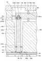
つぎに、第2実施形態に係る第1の同軸管の内部導体610aの固定及び同軸管整合について図10を参照しながら説明する。図10は、第1実施形態を説明する際に使用した図3に対応した図である。第2実施形態では、連結部Dcの構成と、誘電体板近傍に誘電体リングが設けられている点で主に第1実施形態と相異する。よって、以下ではこの相異点を中心に説明し、その他の説明を省略する。(Second Embodiment)
Next, fixation and coaxial tube alignment of the
第2実施形態に係る連結部Dcでは、誘電体ロッド720が、第2の同軸管の内部導体620aの横穴620a3に挿入され、これにより、内部導体620aは外部導体620bに支持される。一方、本実施形態では、誘電体ロッド720は、第1の同軸管の内部導体610aを貫通していないため、内部導体610aの脱落防止の機能は有しない。その替わり、本実施形態では、第2の同軸管の内部導体620aの縦穴620a1の下部がねじ切りされているとともに、内部導体610a端部のロッド610a1の頭部分にもねじが切られている。縦穴620a1の上部はねじ切りされておらず、穴径がロッド610a1の外径よりも大きくなっている。このため、ロッド610a1の頭を縦穴620a1にねじ込んでロッド610a端部のねじが切ってある部分を縦穴620a1上部のねじが切っていない部分に螺合させることにより、ロッド610a1を縦穴620a1に固定する。これにより、第1の同軸管の内部導体610aの脱落を防止しながら、第1の同軸管の内部導体610aを自由に動かせる状態で固定することができる。なお、本実施形態にかかる内部導体610aのロッド610a1と内部導体620aの縦穴620a1との係合部分は、第1の同軸管の内部導体610aが第2の同軸管の内部導体620aから脱落することを防止するための係合部の一例である。 In the connecting portion Dc according to the second embodiment, the
第1の同軸管の内部導体610aには、連結部Dcにて凹部610a4が形成されていて、凹部610a4の内部には、金属バネ730が設けられている。金属バネ730は、第1の同軸管の内部導体610aを誘電体板305に押し付けるバネ部材の一例である。 A recess 610a4 is formed in the
第1の同軸管の内部導体610aの端部は、第2の同軸管の内部導体620aの下部に設けられた凹みに挿入されるようになっている。内部導体610a,620aの接触面には、シールドスパイラル705が設けられている。シールドスパイラル705は、内部導体610aと620aとを電気的に接続する接点部材の一例である。 An end portion of the
第1の同軸管の内部導体610aと外部導体610bとの間には、前述した誘電体リング710の他に、誘電体板305に隣接して誘電体リング735が取り付けられている。これによれば、第1の同軸管610と誘電体板305との隣接部分の強電界部を誘電体で覆うことにより、異常放電を防止することができる。 In addition to the
なお、図10では、金属金具725と誘電体板305との接触面(誘電体板305の窪み部分)には、金属膜305aが設けられていない。 In FIG. 10, the
(第3実施形態)
つぎに、第3実施形態に係る第1の同軸管の内部導体610aの固定及び同軸管整合について図11を参照しながら説明する。図11は、第1実施形態の説明に使用した図3及び第2実施形態の説明に使用した図10に対応した図である。第3実施形態では、連結部Dcの構成が第2実施形態と異なる。よって、以下ではこの相異点を中心に説明し、その他の説明を省略する。(Third embodiment)
Next, fixation and coaxial tube alignment of the
第3実施形態に係る連結部Dcでは、内部導体610aのロッド610a1の外周に凹部610a4が形成され、その外側が板ばね610a5になっている。係合部分にシールドスパイラルは設けられていない。板バネ610a5は、内部導体610aと620aとを電気的に接続する接点部材の一例である。 In the connecting portion Dc according to the third embodiment, a recess 610a4 is formed on the outer periphery of the rod 610a1 of the
第1の同軸管の内部導体610aの凹部610a4には、金属バネ730が設けられていて、金属バネ730(バネ部材の一例)の弾性力により第1の同軸管の内部導体610aを誘電体板305に押しつけて密着させる。 A
以上に説明した各実施形態では、915MHzのマイクロ波を出力するマイクロ波源900を挙げたが、896MHz、922MHz、2.45GHz等のマイクロ波を出力するマイクロ波源であってもよい。また、マイクロ波源は、プラズマを励起するための電磁波を発生する電磁波源の一例であり、100MHz以上の電磁波を出力する電磁波源であれば、マグネトロンや高周波電源も含まれる。 In each of the embodiments described above, the
また、金属電極310の形状は、4角形に限られず、3角形、6角形、8角形でもよい。この場合には、誘電体板305及び金属カバー320の形状も金属電極310の形状と同様になる。金属カバー320やサイドカバーはあってもなくてもよい。金属カバー320がない場合には、蓋体300に直接ガス流路が形成される。また、ガス放出穴がなく、ガス放出機能がなくてもよいし、下段シャワーが設けられていてもよい。金属電極310や誘電体板305の数は8個に限定されず、1個以上の何れかであってもよい。 Further, the shape of the
また、誘電体板305が金属膜305aにて被覆されていない場合、誘電体板305と蓋体300、及び誘電体板305と金属電極310との間の隙間は、0.2mm以下が好ましい。その理由を説明する。誘電体板305と隣接する金属面との間の隙間で放電が起きると、プラズママイクロ波のエネルギーを損失してプラズマ励起効率が著しく悪化するとともに、誘電体305や金属電極310を破損させてしまう。隙間が電子の平均自由行程より小さければ、間隔を狭くすることにより電子がマイクロ波電界から電離に必要なエネルギーを得る前に壁に衝突してエネルギーを失うため、隙間において放電しにくくなる。ガス流路の径は、実使用条件において最も放電しやすい状況においても放電しないような寸法に設定にするべきである。 When the
平均自由行程は、ua/νcで与えられる。ここで、uaは電子の平均速度、νcは電子の衝突周波数である。電子の平均速度uaは、
ua=(8kT/πm)1/2
で与えられる。ここで、kはボルツマン定数、Tは電子温度、mは電子の質量である。隙間で放電が維持される電子温度を3eVとすれば、上式より、ua=1.14×10⁶m/sとなる。The mean free path is given by ua / νc. Here, ua is the average velocity of electrons, and νc is the collision frequency of electrons. The average electron velocity ua is
ua = (8 kT / πm)1/2
Given in. Here, k is a Boltzmann constant, T is an electron temperature, and m is an electron mass. If the electron temperature at which discharge is maintained in the gap is 3 eV, ua = 1.14 × 10⁶ m / s from the above equation.
電子の衝突周波数とマイクロ波角周波数が一致すると、マイクロ波から電子に与えられるエネルギーが最大となり最も放電しやすくなる。マイクロ波周波数が915MHzのとき、νc=5.75×10⁹Hzとなる圧力のとき(アルゴンガスでは約200Pa)最も放電しやすくなる。このときの平均自由行程を上式から計算すると、0.20mmとなる。すなわち、ガス流路の径を0.2mm以下にすれば、隙間で放電することなく常に安定なプラズマを励起することができる。When the electron collision frequency and the microwave angular frequency coincide with each other, the energy given from the microwave to the electron is maximized and the discharge is most easily performed. When the microwave frequency is 915 MHz, discharge is most likely to occur when the pressure is νc = 5.75 × 10⁹ Hz (about 200 Pa for argon gas). When the mean free path at this time is calculated from the above equation, it is 0.20 mm. That is, if the diameter of the gas flow path is 0.2 mm or less, stable plasma can always be excited without discharging in the gap.
以上、添付図面を参照しながら本発明の好適な実施形態について説明したが、本発明は係る例に限定されないことは言うまでもない。当業者であれば、特許請求の範囲に記載された範疇内において、各種の変更例または修正例に想到し得ることは明らかであり、それらについても当然に本発明の技術的範囲に属するものと了解される。 As mentioned above, although preferred embodiment of this invention was described referring an accompanying drawing, it cannot be overemphasized that this invention is not limited to the example which concerns. It will be apparent to those skilled in the art that various changes and modifications can be made within the scope of the claims, and these are naturally within the technical scope of the present invention. Understood.
プラズマ処理装置は、上述したマイクロ波プラズマ処理装置に限られず、成膜処理、拡散処理、エッチング処理、アッシング処理、プラズマドーピング処理など、プラズマにより被処理体を微細加工する装置であればよい。 The plasma processing apparatus is not limited to the above-described microwave plasma processing apparatus, and may be any apparatus that finely processes an object to be processed by plasma, such as a film formation process, a diffusion process, an etching process, an ashing process, or a plasma doping process.
また、たとえば、本発明にかかるプラズマ処理装置は、大面積のガラス基板、円形のシリコンウエハや角型のSOI(Silicon On Insulator)基板を処理することもできる。 Further, for example, the plasma processing apparatus according to the present invention can process a large-area glass substrate, a circular silicon wafer, and a square SOI (Silicon On Insulator) substrate.
10 マイクロ波プラズマ処理装置
100 処理容器
200 容器本体
300 蓋体
300a 上部蓋体
300b 下部蓋体
305 誘電体板
305a 金属膜
310 金属電極
320 金属カバー
325 ねじ
330 主ガス流路
335 細管
350 サイドカバー
610 第1の同軸管
620 第2の同軸管
705、740 シールドスパイラル
710,715,735 誘電体リング
720 誘電体ロッド
725 金属金具
900 マイクロ波源
905 ガス供給源
910 冷媒供給源
Cel ユニットセル
Dc 連結部
DESCRIPTION OF
Claims (17)
Translated fromJapanese処理容器と、
電磁波を出力する電磁波源と、
内部導体の外径と外部導体の内径との比が入力側から出力側に向かう方向に沿って一様でない構造を有し、前記電磁波源から出力された電磁波を伝送させる第1の同軸管と、
前記処理容器の内部に面しかつ前記第1の同軸管に隣接し、前記第1の同軸管を伝送した電磁波を前記処理容器の内部に放出する誘電体板と、を備え、
前記第1の同軸管の外部導体の内径は、入力側と出力側とで実質的に等しく、かつ、入力側から出力側までの間の部分も段差なしで実質的に等しく、
前記第1の同軸管の内部導体の入力側の外径は、前記第1の同軸管の内部導体の出力側の外径より小さく、
前記第1の同軸管の内部導体の外径と外部導体の内径との比は、前記第1の同軸管の電磁波の入力側の特性インピーダンスが前記第1の同軸管の電磁波の出力側の特性インピーダンスよりも大きくなるように定められているプラズマ処理装置。A plasma processing apparatus that plasmas a target object by exciting a gas with electromagnetic waves,
A processing vessel;
An electromagnetic wave source that outputs electromagnetic waves;
A first coaxial waveguide having a structure in which the ratio of the outer diameter of the inner conductor to the inner diameter of the outer conductor is not uniform along the direction from the input side to the output side, and transmits the electromagnetic wave output from the electromagnetic wave source; ,
A dielectric plate that faces the inside of the processing container and is adjacent to the first coaxial waveguide and emits electromagnetic waves transmitted through the first coaxial waveguide to the interior of the processing container;
The inner diameter of the outer conductor of the first coaxial waveguide is substantially equal between the input side and the output side, and the portion between the input side and the output side is also substantially equal without a step,
The outer diameter on the input side of the inner conductor of the first coaxial waveguide is smaller than the outer diameter on the output side of the inner conductor of the first coaxial waveguide,
The ratio between the outer diameter of the inner conductor of the first coaxial waveguide and the inner diameter of the outer conductor is such that the characteristic impedance on the input side of the electromagnetic wave of the first coaxial tube is the characteristic on the output side of the electromagnetic wave of the first coaxial waveguide. A plasma processing apparatus that is determined to be larger than impedance.
前記第1の同軸管の内部導体の外径と外部導体の内径との比は、前記段差部により不連続に変化する請求項1に記載されたプラズマ処理装置。The plasma processing apparatus according to claim 1, wherein a ratio between an outer diameter of the inner conductor of the first coaxial waveguide and an inner diameter of the outer conductor changes discontinuously due to the stepped portion.
前記第1の誘電体支持部材は、前記第1の同軸管の内部導体の外周に形成された溝に嵌入されている請求項1に記載されたプラズマ処理装置。The plasma processing apparatus according to claim 1, wherein the first dielectric support member is fitted in a groove formed on an outer periphery of an inner conductor of the first coaxial waveguide.
前記第1の同軸管の内部導体と前記第2の同軸管の内部導体との連結部に設けられ、前記第1の同軸管の内部導体を直接的または間接的に前記誘電体板に押し付けるバネ部材と、を備える請求項1に記載されたプラズマ処理装置。A spring provided at a connecting portion between the inner conductor of the first coaxial waveguide and the inner conductor of the second coaxial waveguide, and presses the inner conductor of the first coaxial waveguide directly or indirectly against the dielectric plate. A plasma processing apparatus according to claim 1, comprising: a member.
前記第2の誘電体支持部材は、前記第2の同軸管の内部導体の外周に形成された溝に嵌入されている請求項8〜11のいずれかに記載されたプラズマ処理装置。The plasma processing apparatus according to any one of claims 8 to 11, wherein the second dielectric support member is fitted in a groove formed on an outer periphery of an inner conductor of the second coaxial waveguide.
前記誘電体ロッドは、前記第2の同軸管の内部導体に設けられた穴に嵌入されている請求項8〜12のいずれかに記載されたプラズマ処理装置。The plasma processing apparatus according to claim 8, wherein the dielectric rod is fitted into a hole provided in an inner conductor of the second coaxial waveguide.
電磁波源から電磁波を出力し、 Output electromagnetic waves from an electromagnetic source,
電磁波の入力側の特性インピーダンスが出力側の特性インピーダンスよりも大きくなるように、内部導体の外径と外部導体の内径との比が入力側から出力側に向かう方向に沿って一様でない構造を有する第1の同軸管に前記出力した電磁波を伝送し、 A structure in which the ratio between the outer diameter of the inner conductor and the inner diameter of the outer conductor is not uniform along the direction from the input side to the output side so that the characteristic impedance on the input side of the electromagnetic wave is larger than the characteristic impedance on the output side. Transmitting the output electromagnetic wave to a first coaxial pipe having
前記第1の同軸管の外部導体の内径は、入力側と出力側とで実質的に等しく、かつ、入力側から出力側までの間の部分も段差なしで実質的に等しく、 The inner diameter of the outer conductor of the first coaxial waveguide is substantially equal between the input side and the output side, and the portion between the input side and the output side is also substantially equal without a step,
前記第1の同軸管の内部導体の入力側の外径は、前記第1の同軸管の内部導体の出力側の外径より小さく、 The outer diameter on the input side of the inner conductor of the first coaxial waveguide is smaller than the outer diameter on the output side of the inner conductor of the first coaxial waveguide,
前記第1の同軸管を伝送した電磁波を、前記処理容器の内部に面しかつ前記第1の同軸管に隣接した誘電体板から前記処理容器の内部に放出し、 Electromagnetic waves transmitted through the first coaxial waveguide are emitted into the processing container from a dielectric plate facing the interior of the processing container and adjacent to the first coaxial waveguide;
前記放出された電磁波により前記導入されたガスを励起させて被処理体をプラズマ処理するプラズマ処理方法。 A plasma processing method for plasma-treating an object to be processed by exciting the introduced gas with the emitted electromagnetic wave.
Priority Applications (7)
| Application Number | Priority Date | Filing Date | Title |
|---|---|---|---|
| JP2008153423AJP5421551B2 (en) | 2008-06-11 | 2008-06-11 | Plasma processing apparatus and plasma processing method |
| US12/997,180US8327796B2 (en) | 2008-06-11 | 2009-06-03 | Plasma processing apparatus and plasma processing method |
| KR1020127026247AKR20120117949A (en) | 2008-06-11 | 2009-06-03 | Plasma processing device and plasma processing method |
| CN2009801212828ACN102057760A (en) | 2008-06-11 | 2009-06-03 | Plasma processing device and plasma processing method |
| PCT/JP2009/060158WO2009150978A1 (en) | 2008-06-11 | 2009-06-03 | Plasma processing device and plasma processing method |
| KR1020107022951AKR101229843B1 (en) | 2008-06-11 | 2009-06-03 | Plasma processing device |
| TW098119218ATW201012315A (en) | 2008-06-11 | 2009-06-09 | Plasma processing apparatus and plasma processing method |
Applications Claiming Priority (1)
| Application Number | Priority Date | Filing Date | Title |
|---|---|---|---|
| JP2008153423AJP5421551B2 (en) | 2008-06-11 | 2008-06-11 | Plasma processing apparatus and plasma processing method |
Publications (3)
| Publication Number | Publication Date |
|---|---|
| JP2009301807A JP2009301807A (en) | 2009-12-24 |
| JP2009301807A5 JP2009301807A5 (en) | 2011-08-11 |
| JP5421551B2true JP5421551B2 (en) | 2014-02-19 |
Family
ID=41416687
Family Applications (1)
| Application Number | Title | Priority Date | Filing Date |
|---|---|---|---|
| JP2008153423AActiveJP5421551B2 (en) | 2008-06-11 | 2008-06-11 | Plasma processing apparatus and plasma processing method |
Country Status (6)
| Country | Link |
|---|---|
| US (1) | US8327796B2 (en) |
| JP (1) | JP5421551B2 (en) |
| KR (2) | KR101229843B1 (en) |
| CN (1) | CN102057760A (en) |
| TW (1) | TW201012315A (en) |
| WO (1) | WO2009150978A1 (en) |
Families Citing this family (310)
| Publication number | Priority date | Publication date | Assignee | Title |
|---|---|---|---|---|
| JP5520455B2 (en)* | 2008-06-11 | 2014-06-11 | 東京エレクトロン株式会社 | Plasma processing equipment |
| JP5478058B2 (en)* | 2008-12-09 | 2014-04-23 | 国立大学法人東北大学 | Plasma processing equipment |
| US9394608B2 (en) | 2009-04-06 | 2016-07-19 | Asm America, Inc. | Semiconductor processing reactor and components thereof |
| US8802201B2 (en) | 2009-08-14 | 2014-08-12 | Asm America, Inc. | Systems and methods for thin-film deposition of metal oxides using excited nitrogen-oxygen species |
| JP5631088B2 (en)* | 2010-07-15 | 2014-11-26 | 国立大学法人東北大学 | Plasma processing apparatus and plasma processing method |
| US9397380B2 (en)* | 2011-01-28 | 2016-07-19 | Applied Materials, Inc. | Guided wave applicator with non-gaseous dielectric for plasma chamber |
| US20130023129A1 (en) | 2011-07-20 | 2013-01-24 | Asm America, Inc. | Pressure transmitter for a semiconductor processing environment |
| US9017481B1 (en) | 2011-10-28 | 2015-04-28 | Asm America, Inc. | Process feed management for semiconductor substrate processing |
| CN103187224B (en)* | 2011-12-30 | 2015-09-09 | 中微半导体设备(上海)有限公司 | A kind of slide holder for plasma processing apparatus |
| DE102012103938A1 (en)* | 2012-05-04 | 2013-11-07 | Reinhausen Plasma Gmbh | Plasma module for a plasma generating device and plasma generating device |
| US9267205B1 (en)* | 2012-05-30 | 2016-02-23 | Alta Devices, Inc. | Fastener system for supporting a liner plate in a gas showerhead reactor |
| US10714315B2 (en) | 2012-10-12 | 2020-07-14 | Asm Ip Holdings B.V. | Semiconductor reaction chamber showerhead |
| US20160376700A1 (en) | 2013-02-01 | 2016-12-29 | Asm Ip Holding B.V. | System for treatment of deposition reactor |
| DE102013207328A1 (en)* | 2013-04-23 | 2014-10-23 | Siemens Aktiengesellschaft | Apparatus and method for generating high voltage pulses |
| US11015245B2 (en) | 2014-03-19 | 2021-05-25 | Asm Ip Holding B.V. | Gas-phase reactor and system having exhaust plenum and components thereof |
| US10858737B2 (en) | 2014-07-28 | 2020-12-08 | Asm Ip Holding B.V. | Showerhead assembly and components thereof |
| US9890456B2 (en) | 2014-08-21 | 2018-02-13 | Asm Ip Holding B.V. | Method and system for in situ formation of gas-phase compounds |
| US10941490B2 (en) | 2014-10-07 | 2021-03-09 | Asm Ip Holding B.V. | Multiple temperature range susceptor, assembly, reactor and system including the susceptor, and methods of using the same |
| JP6471515B2 (en)* | 2015-01-28 | 2019-02-20 | 日新電機株式会社 | Pipe holding connection structure and high-frequency antenna device including the same |
| US10276355B2 (en) | 2015-03-12 | 2019-04-30 | Asm Ip Holding B.V. | Multi-zone reactor, system including the reactor, and method of using the same |
| DE102015004414A1 (en)* | 2015-04-02 | 2016-10-06 | Centrotherm Photovoltaics Ag | Plasma treatment apparatus for wafers |
| US10458018B2 (en) | 2015-06-26 | 2019-10-29 | Asm Ip Holding B.V. | Structures including metal carbide material, devices including the structures, and methods of forming same |
| US10211308B2 (en) | 2015-10-21 | 2019-02-19 | Asm Ip Holding B.V. | NbMC layers |
| US11139308B2 (en) | 2015-12-29 | 2021-10-05 | Asm Ip Holding B.V. | Atomic layer deposition of III-V compounds to form V-NAND devices |
| WO2017126007A1 (en) | 2016-01-18 | 2017-07-27 | 東芝三菱電機産業システム株式会社 | Activated gas generation device and film-formation treatment device |
| US10529554B2 (en) | 2016-02-19 | 2020-01-07 | Asm Ip Holding B.V. | Method for forming silicon nitride film selectively on sidewalls or flat surfaces of trenches |
| US10343920B2 (en) | 2016-03-18 | 2019-07-09 | Asm Ip Holding B.V. | Aligned carbon nanotubes |
| US10865475B2 (en) | 2016-04-21 | 2020-12-15 | Asm Ip Holding B.V. | Deposition of metal borides and silicides |
| US10190213B2 (en) | 2016-04-21 | 2019-01-29 | Asm Ip Holding B.V. | Deposition of metal borides |
| US10367080B2 (en) | 2016-05-02 | 2019-07-30 | Asm Ip Holding B.V. | Method of forming a germanium oxynitride film |
| US11453943B2 (en) | 2016-05-25 | 2022-09-27 | Asm Ip Holding B.V. | Method for forming carbon-containing silicon/metal oxide or nitride film by ALD using silicon precursor and hydrocarbon precursor |
| US10612137B2 (en) | 2016-07-08 | 2020-04-07 | Asm Ip Holdings B.V. | Organic reactants for atomic layer deposition |
| US9859151B1 (en) | 2016-07-08 | 2018-01-02 | Asm Ip Holding B.V. | Selective film deposition method to form air gaps |
| US9887082B1 (en) | 2016-07-28 | 2018-02-06 | Asm Ip Holding B.V. | Method and apparatus for filling a gap |
| KR102532607B1 (en) | 2016-07-28 | 2023-05-15 | 에이에스엠 아이피 홀딩 비.브이. | Substrate processing apparatus and method of operating the same |
| US9812320B1 (en) | 2016-07-28 | 2017-11-07 | Asm Ip Holding B.V. | Method and apparatus for filling a gap |
| US10643826B2 (en) | 2016-10-26 | 2020-05-05 | Asm Ip Holdings B.V. | Methods for thermally calibrating reaction chambers |
| US11532757B2 (en) | 2016-10-27 | 2022-12-20 | Asm Ip Holding B.V. | Deposition of charge trapping layers |
| US10714350B2 (en) | 2016-11-01 | 2020-07-14 | ASM IP Holdings, B.V. | Methods for forming a transition metal niobium nitride film on a substrate by atomic layer deposition and related semiconductor device structures |
| US10229833B2 (en) | 2016-11-01 | 2019-03-12 | Asm Ip Holding B.V. | Methods for forming a transition metal nitride film on a substrate by atomic layer deposition and related semiconductor device structures |
| KR102546317B1 (en) | 2016-11-15 | 2023-06-21 | 에이에스엠 아이피 홀딩 비.브이. | Gas supply unit and substrate processing apparatus including the same |
| KR102762543B1 (en)* | 2016-12-14 | 2025-02-05 | 에이에스엠 아이피 홀딩 비.브이. | Substrate processing apparatus |
| US11447861B2 (en) | 2016-12-15 | 2022-09-20 | Asm Ip Holding B.V. | Sequential infiltration synthesis apparatus and a method of forming a patterned structure |
| US11581186B2 (en) | 2016-12-15 | 2023-02-14 | Asm Ip Holding B.V. | Sequential infiltration synthesis apparatus |
| KR102700194B1 (en) | 2016-12-19 | 2024-08-28 | 에이에스엠 아이피 홀딩 비.브이. | Substrate processing apparatus |
| US10269558B2 (en) | 2016-12-22 | 2019-04-23 | Asm Ip Holding B.V. | Method of forming a structure on a substrate |
| US10867788B2 (en) | 2016-12-28 | 2020-12-15 | Asm Ip Holding B.V. | Method of forming a structure on a substrate |
| US11390950B2 (en) | 2017-01-10 | 2022-07-19 | Asm Ip Holding B.V. | Reactor system and method to reduce residue buildup during a film deposition process |
| US10468261B2 (en) | 2017-02-15 | 2019-11-05 | Asm Ip Holding B.V. | Methods for forming a metallic film on a substrate by cyclical deposition and related semiconductor device structures |
| US10529563B2 (en) | 2017-03-29 | 2020-01-07 | Asm Ip Holdings B.V. | Method for forming doped metal oxide films on a substrate by cyclical deposition and related semiconductor device structures |
| KR102457289B1 (en) | 2017-04-25 | 2022-10-21 | 에이에스엠 아이피 홀딩 비.브이. | Method for depositing a thin film and manufacturing a semiconductor device |
| US10892156B2 (en) | 2017-05-08 | 2021-01-12 | Asm Ip Holding B.V. | Methods for forming a silicon nitride film on a substrate and related semiconductor device structures |
| US10770286B2 (en) | 2017-05-08 | 2020-09-08 | Asm Ip Holdings B.V. | Methods for selectively forming a silicon nitride film on a substrate and related semiconductor device structures |
| US10886123B2 (en) | 2017-06-02 | 2021-01-05 | Asm Ip Holding B.V. | Methods for forming low temperature semiconductor layers and related semiconductor device structures |
| US12040200B2 (en) | 2017-06-20 | 2024-07-16 | Asm Ip Holding B.V. | Semiconductor processing apparatus and methods for calibrating a semiconductor processing apparatus |
| US11306395B2 (en) | 2017-06-28 | 2022-04-19 | Asm Ip Holding B.V. | Methods for depositing a transition metal nitride film on a substrate by atomic layer deposition and related deposition apparatus |
| KR20190009245A (en) | 2017-07-18 | 2019-01-28 | 에이에스엠 아이피 홀딩 비.브이. | Methods for forming a semiconductor device structure and related semiconductor device structures |
| US11374112B2 (en) | 2017-07-19 | 2022-06-28 | Asm Ip Holding B.V. | Method for depositing a group IV semiconductor and related semiconductor device structures |
| US10541333B2 (en) | 2017-07-19 | 2020-01-21 | Asm Ip Holding B.V. | Method for depositing a group IV semiconductor and related semiconductor device structures |
| US11018002B2 (en) | 2017-07-19 | 2021-05-25 | Asm Ip Holding B.V. | Method for selectively depositing a Group IV semiconductor and related semiconductor device structures |
| US10590535B2 (en) | 2017-07-26 | 2020-03-17 | Asm Ip Holdings B.V. | Chemical treatment, deposition and/or infiltration apparatus and method for using the same |
| TWI815813B (en) | 2017-08-04 | 2023-09-21 | 荷蘭商Asm智慧財產控股公司 | Showerhead assembly for distributing a gas within a reaction chamber |
| US10770336B2 (en) | 2017-08-08 | 2020-09-08 | Asm Ip Holding B.V. | Substrate lift mechanism and reactor including same |
| US10692741B2 (en) | 2017-08-08 | 2020-06-23 | Asm Ip Holdings B.V. | Radiation shield |
| US11139191B2 (en) | 2017-08-09 | 2021-10-05 | Asm Ip Holding B.V. | Storage apparatus for storing cassettes for substrates and processing apparatus equipped therewith |
| US11769682B2 (en) | 2017-08-09 | 2023-09-26 | Asm Ip Holding B.V. | Storage apparatus for storing cassettes for substrates and processing apparatus equipped therewith |
| US11830730B2 (en) | 2017-08-29 | 2023-11-28 | Asm Ip Holding B.V. | Layer forming method and apparatus |
| US11056344B2 (en) | 2017-08-30 | 2021-07-06 | Asm Ip Holding B.V. | Layer forming method |
| KR102491945B1 (en) | 2017-08-30 | 2023-01-26 | 에이에스엠 아이피 홀딩 비.브이. | Substrate processing apparatus |
| US11295980B2 (en) | 2017-08-30 | 2022-04-05 | Asm Ip Holding B.V. | Methods for depositing a molybdenum metal film over a dielectric surface of a substrate by a cyclical deposition process and related semiconductor device structures |
| KR102401446B1 (en) | 2017-08-31 | 2022-05-24 | 에이에스엠 아이피 홀딩 비.브이. | Substrate processing apparatus |
| KR102630301B1 (en) | 2017-09-21 | 2024-01-29 | 에이에스엠 아이피 홀딩 비.브이. | Method of sequential infiltration synthesis treatment of infiltrateable material and structures and devices formed using same |
| US10844484B2 (en) | 2017-09-22 | 2020-11-24 | Asm Ip Holding B.V. | Apparatus for dispensing a vapor phase reactant to a reaction chamber and related methods |
| US10658205B2 (en) | 2017-09-28 | 2020-05-19 | Asm Ip Holdings B.V. | Chemical dispensing apparatus and methods for dispensing a chemical to a reaction chamber |
| US10403504B2 (en) | 2017-10-05 | 2019-09-03 | Asm Ip Holding B.V. | Method for selectively depositing a metallic film on a substrate |
| US10923344B2 (en) | 2017-10-30 | 2021-02-16 | Asm Ip Holding B.V. | Methods for forming a semiconductor structure and related semiconductor structures |
| US10910262B2 (en) | 2017-11-16 | 2021-02-02 | Asm Ip Holding B.V. | Method of selectively depositing a capping layer structure on a semiconductor device structure |
| US11022879B2 (en) | 2017-11-24 | 2021-06-01 | Asm Ip Holding B.V. | Method of forming an enhanced unexposed photoresist layer |
| CN111344522B (en) | 2017-11-27 | 2022-04-12 | 阿斯莫Ip控股公司 | Including clean mini-environment device |
| WO2019103613A1 (en) | 2017-11-27 | 2019-05-31 | Asm Ip Holding B.V. | A storage device for storing wafer cassettes for use with a batch furnace |
| US10872771B2 (en) | 2018-01-16 | 2020-12-22 | Asm Ip Holding B. V. | Method for depositing a material film on a substrate within a reaction chamber by a cyclical deposition process and related device structures |
| TWI799494B (en) | 2018-01-19 | 2023-04-21 | 荷蘭商Asm 智慧財產控股公司 | Deposition method |
| KR102695659B1 (en) | 2018-01-19 | 2024-08-14 | 에이에스엠 아이피 홀딩 비.브이. | Method for depositing a gap filling layer by plasma assisted deposition |
| US11018047B2 (en) | 2018-01-25 | 2021-05-25 | Asm Ip Holding B.V. | Hybrid lift pin |
| USD880437S1 (en) | 2018-02-01 | 2020-04-07 | Asm Ip Holding B.V. | Gas supply plate for semiconductor manufacturing apparatus |
| US11081345B2 (en) | 2018-02-06 | 2021-08-03 | Asm Ip Holding B.V. | Method of post-deposition treatment for silicon oxide film |
| WO2019158960A1 (en) | 2018-02-14 | 2019-08-22 | Asm Ip Holding B.V. | A method for depositing a ruthenium-containing film on a substrate by a cyclical deposition process |
| US10896820B2 (en) | 2018-02-14 | 2021-01-19 | Asm Ip Holding B.V. | Method for depositing a ruthenium-containing film on a substrate by a cyclical deposition process |
| US10731249B2 (en) | 2018-02-15 | 2020-08-04 | Asm Ip Holding B.V. | Method of forming a transition metal containing film on a substrate by a cyclical deposition process, a method for supplying a transition metal halide compound to a reaction chamber, and related vapor deposition apparatus |
| KR102636427B1 (en) | 2018-02-20 | 2024-02-13 | 에이에스엠 아이피 홀딩 비.브이. | Substrate processing method and apparatus |
| US10975470B2 (en) | 2018-02-23 | 2021-04-13 | Asm Ip Holding B.V. | Apparatus for detecting or monitoring for a chemical precursor in a high temperature environment |
| US11473195B2 (en) | 2018-03-01 | 2022-10-18 | Asm Ip Holding B.V. | Semiconductor processing apparatus and a method for processing a substrate |
| US11629406B2 (en) | 2018-03-09 | 2023-04-18 | Asm Ip Holding B.V. | Semiconductor processing apparatus comprising one or more pyrometers for measuring a temperature of a substrate during transfer of the substrate |
| US11114283B2 (en) | 2018-03-16 | 2021-09-07 | Asm Ip Holding B.V. | Reactor, system including the reactor, and methods of manufacturing and using same |
| KR102646467B1 (en) | 2018-03-27 | 2024-03-11 | 에이에스엠 아이피 홀딩 비.브이. | Method of forming an electrode on a substrate and a semiconductor device structure including an electrode |
| US11230766B2 (en) | 2018-03-29 | 2022-01-25 | Asm Ip Holding B.V. | Substrate processing apparatus and method |
| US11088002B2 (en) | 2018-03-29 | 2021-08-10 | Asm Ip Holding B.V. | Substrate rack and a substrate processing system and method |
| KR102501472B1 (en) | 2018-03-30 | 2023-02-20 | 에이에스엠 아이피 홀딩 비.브이. | Substrate processing method |
| KR102600229B1 (en) | 2018-04-09 | 2023-11-10 | 에이에스엠 아이피 홀딩 비.브이. | Substrate supporting device, substrate processing apparatus including the same and substrate processing method |
| TWI811348B (en) | 2018-05-08 | 2023-08-11 | 荷蘭商Asm 智慧財產控股公司 | Methods for depositing an oxide film on a substrate by a cyclical deposition process and related device structures |
| US12025484B2 (en) | 2018-05-08 | 2024-07-02 | Asm Ip Holding B.V. | Thin film forming method |
| US12272527B2 (en) | 2018-05-09 | 2025-04-08 | Asm Ip Holding B.V. | Apparatus for use with hydrogen radicals and method of using same |
| KR20190129718A (en) | 2018-05-11 | 2019-11-20 | 에이에스엠 아이피 홀딩 비.브이. | Methods for forming a doped metal carbide film on a substrate and related semiconductor device structures |
| KR102596988B1 (en) | 2018-05-28 | 2023-10-31 | 에이에스엠 아이피 홀딩 비.브이. | Method of processing a substrate and a device manufactured by the same |
| US11718913B2 (en) | 2018-06-04 | 2023-08-08 | Asm Ip Holding B.V. | Gas distribution system and reactor system including same |
| TWI840362B (en) | 2018-06-04 | 2024-05-01 | 荷蘭商Asm Ip私人控股有限公司 | Wafer handling chamber with moisture reduction |
| US11286562B2 (en) | 2018-06-08 | 2022-03-29 | Asm Ip Holding B.V. | Gas-phase chemical reactor and method of using same |
| US10797133B2 (en) | 2018-06-21 | 2020-10-06 | Asm Ip Holding B.V. | Method for depositing a phosphorus doped silicon arsenide film and related semiconductor device structures |
| KR102568797B1 (en) | 2018-06-21 | 2023-08-21 | 에이에스엠 아이피 홀딩 비.브이. | Substrate processing system |
| TWI873894B (en) | 2018-06-27 | 2025-02-21 | 荷蘭商Asm Ip私人控股有限公司 | Cyclic deposition methods for forming metal-containing material and films and structures including the metal-containing material |
| KR102854019B1 (en) | 2018-06-27 | 2025-09-02 | 에이에스엠 아이피 홀딩 비.브이. | Periodic deposition method for forming a metal-containing material and films and structures comprising the metal-containing material |
| KR102686758B1 (en) | 2018-06-29 | 2024-07-18 | 에이에스엠 아이피 홀딩 비.브이. | Method for depositing a thin film and manufacturing a semiconductor device |
| US10612136B2 (en) | 2018-06-29 | 2020-04-07 | ASM IP Holding, B.V. | Temperature-controlled flange and reactor system including same |
| US10755922B2 (en) | 2018-07-03 | 2020-08-25 | Asm Ip Holding B.V. | Method for depositing silicon-free carbon-containing film as gap-fill layer by pulse plasma-assisted deposition |
| US10388513B1 (en) | 2018-07-03 | 2019-08-20 | Asm Ip Holding B.V. | Method for depositing silicon-free carbon-containing film as gap-fill layer by pulse plasma-assisted deposition |
| US10767789B2 (en) | 2018-07-16 | 2020-09-08 | Asm Ip Holding B.V. | Diaphragm valves, valve components, and methods for forming valve components |
| US11053591B2 (en) | 2018-08-06 | 2021-07-06 | Asm Ip Holding B.V. | Multi-port gas injection system and reactor system including same |
| US10883175B2 (en) | 2018-08-09 | 2021-01-05 | Asm Ip Holding B.V. | Vertical furnace for processing substrates and a liner for use therein |
| US10829852B2 (en) | 2018-08-16 | 2020-11-10 | Asm Ip Holding B.V. | Gas distribution device for a wafer processing apparatus |
| US11430674B2 (en) | 2018-08-22 | 2022-08-30 | Asm Ip Holding B.V. | Sensor array, apparatus for dispensing a vapor phase reactant to a reaction chamber and related methods |
| US11024523B2 (en) | 2018-09-11 | 2021-06-01 | Asm Ip Holding B.V. | Substrate processing apparatus and method |
| KR102707956B1 (en) | 2018-09-11 | 2024-09-19 | 에이에스엠 아이피 홀딩 비.브이. | Method for deposition of a thin film |
| US11049751B2 (en) | 2018-09-14 | 2021-06-29 | Asm Ip Holding B.V. | Cassette supply system to store and handle cassettes and processing apparatus equipped therewith |
| CN110970344B (en) | 2018-10-01 | 2024-10-25 | Asmip控股有限公司 | Substrate holding apparatus, system comprising the same and method of using the same |
| US11232963B2 (en) | 2018-10-03 | 2022-01-25 | Asm Ip Holding B.V. | Substrate processing apparatus and method |
| KR102592699B1 (en) | 2018-10-08 | 2023-10-23 | 에이에스엠 아이피 홀딩 비.브이. | Substrate support unit and apparatuses for depositing thin film and processing the substrate including the same |
| KR102605121B1 (en) | 2018-10-19 | 2023-11-23 | 에이에스엠 아이피 홀딩 비.브이. | Substrate processing apparatus and substrate processing method |
| KR102546322B1 (en) | 2018-10-19 | 2023-06-21 | 에이에스엠 아이피 홀딩 비.브이. | Substrate processing apparatus and substrate processing method |
| USD948463S1 (en) | 2018-10-24 | 2022-04-12 | Asm Ip Holding B.V. | Susceptor for semiconductor substrate supporting apparatus |
| US12378665B2 (en) | 2018-10-26 | 2025-08-05 | Asm Ip Holding B.V. | High temperature coatings for a preclean and etch apparatus and related methods |
| US11087997B2 (en) | 2018-10-31 | 2021-08-10 | Asm Ip Holding B.V. | Substrate processing apparatus for processing substrates |
| KR102748291B1 (en) | 2018-11-02 | 2024-12-31 | 에이에스엠 아이피 홀딩 비.브이. | Substrate support unit and substrate processing apparatus including the same |
| US11572620B2 (en) | 2018-11-06 | 2023-02-07 | Asm Ip Holding B.V. | Methods for selectively depositing an amorphous silicon film on a substrate |
| US11031242B2 (en) | 2018-11-07 | 2021-06-08 | Asm Ip Holding B.V. | Methods for depositing a boron doped silicon germanium film |
| US10847366B2 (en) | 2018-11-16 | 2020-11-24 | Asm Ip Holding B.V. | Methods for depositing a transition metal chalcogenide film on a substrate by a cyclical deposition process |
| US10818758B2 (en) | 2018-11-16 | 2020-10-27 | Asm Ip Holding B.V. | Methods for forming a metal silicate film on a substrate in a reaction chamber and related semiconductor device structures |
| US12040199B2 (en) | 2018-11-28 | 2024-07-16 | Asm Ip Holding B.V. | Substrate processing apparatus for processing substrates |
| US11217444B2 (en) | 2018-11-30 | 2022-01-04 | Asm Ip Holding B.V. | Method for forming an ultraviolet radiation responsive metal oxide-containing film |
| KR102636428B1 (en) | 2018-12-04 | 2024-02-13 | 에이에스엠 아이피 홀딩 비.브이. | A method for cleaning a substrate processing apparatus |
| JP7125058B2 (en)* | 2018-12-06 | 2022-08-24 | 東京エレクトロン株式会社 | Plasma processing apparatus and plasma processing method |
| US11158513B2 (en) | 2018-12-13 | 2021-10-26 | Asm Ip Holding B.V. | Methods for forming a rhenium-containing film on a substrate by a cyclical deposition process and related semiconductor device structures |
| TWI874340B (en) | 2018-12-14 | 2025-03-01 | 荷蘭商Asm Ip私人控股有限公司 | Method of forming device structure, structure formed by the method and system for performing the method |
| TWI866480B (en) | 2019-01-17 | 2024-12-11 | 荷蘭商Asm Ip 私人控股有限公司 | Methods of forming a transition metal containing film on a substrate by a cyclical deposition process |
| KR102727227B1 (en) | 2019-01-22 | 2024-11-07 | 에이에스엠 아이피 홀딩 비.브이. | Semiconductor processing device |
| CN111524788B (en) | 2019-02-01 | 2023-11-24 | Asm Ip私人控股有限公司 | Method for forming topologically selective films of silicon oxide |
| TWI838458B (en) | 2019-02-20 | 2024-04-11 | 荷蘭商Asm Ip私人控股有限公司 | Apparatus and methods for plug fill deposition in 3-d nand applications |
| TWI845607B (en) | 2019-02-20 | 2024-06-21 | 荷蘭商Asm Ip私人控股有限公司 | Cyclical deposition method and apparatus for filling a recess formed within a substrate surface |
| TWI873122B (en) | 2019-02-20 | 2025-02-21 | 荷蘭商Asm Ip私人控股有限公司 | Method of filling a recess formed within a surface of a substrate, semiconductor structure formed according to the method, and semiconductor processing apparatus |
| KR102626263B1 (en) | 2019-02-20 | 2024-01-16 | 에이에스엠 아이피 홀딩 비.브이. | Cyclical deposition method including treatment step and apparatus for same |
| TWI842826B (en) | 2019-02-22 | 2024-05-21 | 荷蘭商Asm Ip私人控股有限公司 | Substrate processing apparatus and method for processing substrate |
| US11742198B2 (en) | 2019-03-08 | 2023-08-29 | Asm Ip Holding B.V. | Structure including SiOCN layer and method of forming same |
| KR102782593B1 (en) | 2019-03-08 | 2025-03-14 | 에이에스엠 아이피 홀딩 비.브이. | Structure Including SiOC Layer and Method of Forming Same |
| KR102858005B1 (en) | 2019-03-08 | 2025-09-09 | 에이에스엠 아이피 홀딩 비.브이. | Method for Selective Deposition of Silicon Nitride Layer and Structure Including Selectively-Deposited Silicon Nitride Layer |
| JP2020167398A (en) | 2019-03-28 | 2020-10-08 | エーエスエム・アイピー・ホールディング・ベー・フェー | Door openers and substrate processing equipment provided with door openers |
| KR102809999B1 (en) | 2019-04-01 | 2025-05-19 | 에이에스엠 아이피 홀딩 비.브이. | Method of manufacturing semiconductor device |
| KR20200123380A (en) | 2019-04-19 | 2020-10-29 | 에이에스엠 아이피 홀딩 비.브이. | Layer forming method and apparatus |
| KR20200125453A (en) | 2019-04-24 | 2020-11-04 | 에이에스엠 아이피 홀딩 비.브이. | Gas-phase reactor system and method of using same |
| KR20200130121A (en) | 2019-05-07 | 2020-11-18 | 에이에스엠 아이피 홀딩 비.브이. | Chemical source vessel with dip tube |
| US11289326B2 (en) | 2019-05-07 | 2022-03-29 | Asm Ip Holding B.V. | Method for reforming amorphous carbon polymer film |
| KR20200130652A (en) | 2019-05-10 | 2020-11-19 | 에이에스엠 아이피 홀딩 비.브이. | Method of depositing material onto a surface and structure formed according to the method |
| JP7598201B2 (en) | 2019-05-16 | 2024-12-11 | エーエスエム・アイピー・ホールディング・ベー・フェー | Wafer boat handling apparatus, vertical batch furnace and method |
| JP7612342B2 (en) | 2019-05-16 | 2025-01-14 | エーエスエム・アイピー・ホールディング・ベー・フェー | Wafer boat handling apparatus, vertical batch furnace and method |
| USD947913S1 (en) | 2019-05-17 | 2022-04-05 | Asm Ip Holding B.V. | Susceptor shaft |
| USD975665S1 (en) | 2019-05-17 | 2023-01-17 | Asm Ip Holding B.V. | Susceptor shaft |
| USD935572S1 (en) | 2019-05-24 | 2021-11-09 | Asm Ip Holding B.V. | Gas channel plate |
| USD922229S1 (en) | 2019-06-05 | 2021-06-15 | Asm Ip Holding B.V. | Device for controlling a temperature of a gas supply unit |
| KR20200141002A (en) | 2019-06-06 | 2020-12-17 | 에이에스엠 아이피 홀딩 비.브이. | Method of using a gas-phase reactor system including analyzing exhausted gas |
| KR20200141931A (en) | 2019-06-10 | 2020-12-21 | 에이에스엠 아이피 홀딩 비.브이. | Method for cleaning quartz epitaxial chambers |
| KR20200143254A (en) | 2019-06-11 | 2020-12-23 | 에이에스엠 아이피 홀딩 비.브이. | Method of forming an electronic structure using an reforming gas, system for performing the method, and structure formed using the method |
| USD944946S1 (en) | 2019-06-14 | 2022-03-01 | Asm Ip Holding B.V. | Shower plate |
| USD931978S1 (en) | 2019-06-27 | 2021-09-28 | Asm Ip Holding B.V. | Showerhead vacuum transport |
| KR20210005515A (en) | 2019-07-03 | 2021-01-14 | 에이에스엠 아이피 홀딩 비.브이. | Temperature control assembly for substrate processing apparatus and method of using same |
| JP7499079B2 (en) | 2019-07-09 | 2024-06-13 | エーエスエム・アイピー・ホールディング・ベー・フェー | Plasma device using coaxial waveguide and substrate processing method |
| CN112216646A (en) | 2019-07-10 | 2021-01-12 | Asm Ip私人控股有限公司 | Substrate supporting assembly and substrate processing device comprising same |
| KR20210010307A (en) | 2019-07-16 | 2021-01-27 | 에이에스엠 아이피 홀딩 비.브이. | Substrate processing apparatus |
| KR20210010816A (en) | 2019-07-17 | 2021-01-28 | 에이에스엠 아이피 홀딩 비.브이. | Radical assist ignition plasma system and method |
| KR102860110B1 (en) | 2019-07-17 | 2025-09-16 | 에이에스엠 아이피 홀딩 비.브이. | Methods of forming silicon germanium structures |
| US11643724B2 (en) | 2019-07-18 | 2023-05-09 | Asm Ip Holding B.V. | Method of forming structures using a neutral beam |
| TWI839544B (en) | 2019-07-19 | 2024-04-21 | 荷蘭商Asm Ip私人控股有限公司 | Method of forming topology-controlled amorphous carbon polymer film |
| KR20210010817A (en) | 2019-07-19 | 2021-01-28 | 에이에스엠 아이피 홀딩 비.브이. | Method of Forming Topology-Controlled Amorphous Carbon Polymer Film |
| TWI851767B (en) | 2019-07-29 | 2024-08-11 | 荷蘭商Asm Ip私人控股有限公司 | Methods for selective deposition utilizing n-type dopants and/or alternative dopants to achieve high dopant incorporation |
| CN112309899A (en) | 2019-07-30 | 2021-02-02 | Asm Ip私人控股有限公司 | Substrate processing apparatus |
| US12169361B2 (en) | 2019-07-30 | 2024-12-17 | Asm Ip Holding B.V. | Substrate processing apparatus and method |
| CN112309900A (en) | 2019-07-30 | 2021-02-02 | Asm Ip私人控股有限公司 | Substrate processing apparatus |
| US11227782B2 (en) | 2019-07-31 | 2022-01-18 | Asm Ip Holding B.V. | Vertical batch furnace assembly |
| US11587815B2 (en) | 2019-07-31 | 2023-02-21 | Asm Ip Holding B.V. | Vertical batch furnace assembly |
| US11587814B2 (en) | 2019-07-31 | 2023-02-21 | Asm Ip Holding B.V. | Vertical batch furnace assembly |
| CN112323048B (en) | 2019-08-05 | 2024-02-09 | Asm Ip私人控股有限公司 | Liquid level sensor for chemical source container |
| CN112342526A (en) | 2019-08-09 | 2021-02-09 | Asm Ip私人控股有限公司 | Heater assembly including cooling device and method of using same |
| USD965044S1 (en) | 2019-08-19 | 2022-09-27 | Asm Ip Holding B.V. | Susceptor shaft |
| USD965524S1 (en) | 2019-08-19 | 2022-10-04 | Asm Ip Holding B.V. | Susceptor support |
| JP2021031769A (en) | 2019-08-21 | 2021-03-01 | エーエスエム アイピー ホールディング ビー.ブイ. | Production apparatus of mixed gas of film deposition raw material and film deposition apparatus |
| USD949319S1 (en) | 2019-08-22 | 2022-04-19 | Asm Ip Holding B.V. | Exhaust duct |
| KR20210024423A (en) | 2019-08-22 | 2021-03-05 | 에이에스엠 아이피 홀딩 비.브이. | Method for forming a structure with a hole |
| USD979506S1 (en) | 2019-08-22 | 2023-02-28 | Asm Ip Holding B.V. | Insulator |
| USD940837S1 (en) | 2019-08-22 | 2022-01-11 | Asm Ip Holding B.V. | Electrode |
| USD930782S1 (en) | 2019-08-22 | 2021-09-14 | Asm Ip Holding B.V. | Gas distributor |
| KR20210024420A (en) | 2019-08-23 | 2021-03-05 | 에이에스엠 아이피 홀딩 비.브이. | Method for depositing silicon oxide film having improved quality by peald using bis(diethylamino)silane |
| US11286558B2 (en) | 2019-08-23 | 2022-03-29 | Asm Ip Holding B.V. | Methods for depositing a molybdenum nitride film on a surface of a substrate by a cyclical deposition process and related semiconductor device structures including a molybdenum nitride film |
| KR102806450B1 (en) | 2019-09-04 | 2025-05-12 | 에이에스엠 아이피 홀딩 비.브이. | Methods for selective deposition using a sacrificial capping layer |
| KR102733104B1 (en) | 2019-09-05 | 2024-11-22 | 에이에스엠 아이피 홀딩 비.브이. | Substrate processing apparatus |
| US11562901B2 (en) | 2019-09-25 | 2023-01-24 | Asm Ip Holding B.V. | Substrate processing method |
| CN112593212B (en) | 2019-10-02 | 2023-12-22 | Asm Ip私人控股有限公司 | Method for forming topologically selective silicon oxide film by cyclic plasma enhanced deposition process |
| TW202128273A (en) | 2019-10-08 | 2021-08-01 | 荷蘭商Asm Ip私人控股有限公司 | Gas injection system, reactor system, and method of depositing material on surface of substratewithin reaction chamber |
| TWI846953B (en) | 2019-10-08 | 2024-07-01 | 荷蘭商Asm Ip私人控股有限公司 | Substrate processing device |
| KR20210042810A (en) | 2019-10-08 | 2021-04-20 | 에이에스엠 아이피 홀딩 비.브이. | Reactor system including a gas distribution assembly for use with activated species and method of using same |
| TWI846966B (en) | 2019-10-10 | 2024-07-01 | 荷蘭商Asm Ip私人控股有限公司 | Method of forming a photoresist underlayer and structure including same |
| US12009241B2 (en) | 2019-10-14 | 2024-06-11 | Asm Ip Holding B.V. | Vertical batch furnace assembly with detector to detect cassette |
| TWI834919B (en) | 2019-10-16 | 2024-03-11 | 荷蘭商Asm Ip私人控股有限公司 | Method of topology-selective film formation of silicon oxide |
| US11637014B2 (en) | 2019-10-17 | 2023-04-25 | Asm Ip Holding B.V. | Methods for selective deposition of doped semiconductor material |
| KR102845724B1 (en) | 2019-10-21 | 2025-08-13 | 에이에스엠 아이피 홀딩 비.브이. | Apparatus and methods for selectively etching films |
| KR20210050453A (en) | 2019-10-25 | 2021-05-07 | 에이에스엠 아이피 홀딩 비.브이. | Methods for filling a gap feature on a substrate surface and related semiconductor structures |
| US11646205B2 (en) | 2019-10-29 | 2023-05-09 | Asm Ip Holding B.V. | Methods of selectively forming n-type doped material on a surface, systems for selectively forming n-type doped material, and structures formed using same |
| KR20210054983A (en) | 2019-11-05 | 2021-05-14 | 에이에스엠 아이피 홀딩 비.브이. | Structures with doped semiconductor layers and methods and systems for forming same |
| US11501968B2 (en) | 2019-11-15 | 2022-11-15 | Asm Ip Holding B.V. | Method for providing a semiconductor device with silicon filled gaps |
| KR102861314B1 (en) | 2019-11-20 | 2025-09-17 | 에이에스엠 아이피 홀딩 비.브이. | Method of depositing carbon-containing material on a surface of a substrate, structure formed using the method, and system for forming the structure |
| CN112951697B (en) | 2019-11-26 | 2025-07-29 | Asmip私人控股有限公司 | Substrate processing apparatus |
| US11450529B2 (en) | 2019-11-26 | 2022-09-20 | Asm Ip Holding B.V. | Methods for selectively forming a target film on a substrate comprising a first dielectric surface and a second metallic surface |
| CN120432376A (en) | 2019-11-29 | 2025-08-05 | Asm Ip私人控股有限公司 | Substrate processing apparatus |
| CN112885692B (en) | 2019-11-29 | 2025-08-15 | Asmip私人控股有限公司 | Substrate processing apparatus |
| JP7527928B2 (en) | 2019-12-02 | 2024-08-05 | エーエスエム・アイピー・ホールディング・ベー・フェー | Substrate processing apparatus and substrate processing method |
| KR20210070898A (en) | 2019-12-04 | 2021-06-15 | 에이에스엠 아이피 홀딩 비.브이. | Substrate processing apparatus |
| KR20210078405A (en) | 2019-12-17 | 2021-06-28 | 에이에스엠 아이피 홀딩 비.브이. | Method of forming vanadium nitride layer and structure including the vanadium nitride layer |
| KR20210080214A (en) | 2019-12-19 | 2021-06-30 | 에이에스엠 아이피 홀딩 비.브이. | Methods for filling a gap feature on a substrate and related semiconductor structures |
| JP7636892B2 (en) | 2020-01-06 | 2025-02-27 | エーエスエム・アイピー・ホールディング・ベー・フェー | Channeled Lift Pins |
| JP7730637B2 (en) | 2020-01-06 | 2025-08-28 | エーエスエム・アイピー・ホールディング・ベー・フェー | Gas delivery assembly, components thereof, and reactor system including same |
| US11993847B2 (en) | 2020-01-08 | 2024-05-28 | Asm Ip Holding B.V. | Injector |
| KR20210093163A (en) | 2020-01-16 | 2021-07-27 | 에이에스엠 아이피 홀딩 비.브이. | Method of forming high aspect ratio features |
| KR102675856B1 (en) | 2020-01-20 | 2024-06-17 | 에이에스엠 아이피 홀딩 비.브이. | Method of forming thin film and method of modifying surface of thin film |
| TWI889744B (en) | 2020-01-29 | 2025-07-11 | 荷蘭商Asm Ip私人控股有限公司 | Contaminant trap system, and baffle plate stack |
| TW202513845A (en) | 2020-02-03 | 2025-04-01 | 荷蘭商Asm Ip私人控股有限公司 | Semiconductor structures and methods for forming the same |
| KR20210100010A (en) | 2020-02-04 | 2021-08-13 | 에이에스엠 아이피 홀딩 비.브이. | Method and apparatus for transmittance measurements of large articles |
| US11776846B2 (en) | 2020-02-07 | 2023-10-03 | Asm Ip Holding B.V. | Methods for depositing gap filling fluids and related systems and devices |
| TW202146691A (en) | 2020-02-13 | 2021-12-16 | 荷蘭商Asm Ip私人控股有限公司 | Gas distribution assembly, shower plate assembly, and method of adjusting conductance of gas to reaction chamber |
| KR20210103956A (en) | 2020-02-13 | 2021-08-24 | 에이에스엠 아이피 홀딩 비.브이. | Substrate processing apparatus including light receiving device and calibration method of light receiving device |
| TWI855223B (en) | 2020-02-17 | 2024-09-11 | 荷蘭商Asm Ip私人控股有限公司 | Method for growing phosphorous-doped silicon layer |
| CN113410160A (en) | 2020-02-28 | 2021-09-17 | Asm Ip私人控股有限公司 | System specially used for cleaning parts |
| KR20210113043A (en) | 2020-03-04 | 2021-09-15 | 에이에스엠 아이피 홀딩 비.브이. | Alignment fixture for a reactor system |
| KR20210116240A (en) | 2020-03-11 | 2021-09-27 | 에이에스엠 아이피 홀딩 비.브이. | Substrate handling device with adjustable joints |
| US11876356B2 (en) | 2020-03-11 | 2024-01-16 | Asm Ip Holding B.V. | Lockout tagout assembly and system and method of using same |
| KR102775390B1 (en) | 2020-03-12 | 2025-02-28 | 에이에스엠 아이피 홀딩 비.브이. | Method for Fabricating Layer Structure Having Target Topological Profile |
| US12173404B2 (en) | 2020-03-17 | 2024-12-24 | Asm Ip Holding B.V. | Method of depositing epitaxial material, structure formed using the method, and system for performing the method |
| WO2021192810A1 (en)* | 2020-03-23 | 2021-09-30 | 株式会社エス・エス・ティ | High frequency reaction treatment device and high frequency reaction treatment system |
| KR102755229B1 (en) | 2020-04-02 | 2025-01-14 | 에이에스엠 아이피 홀딩 비.브이. | Thin film forming method |
| TWI887376B (en) | 2020-04-03 | 2025-06-21 | 荷蘭商Asm Ip私人控股有限公司 | Method for manufacturing semiconductor device |
| TWI888525B (en) | 2020-04-08 | 2025-07-01 | 荷蘭商Asm Ip私人控股有限公司 | Apparatus and methods for selectively etching silcon oxide films |
| KR20210128343A (en) | 2020-04-15 | 2021-10-26 | 에이에스엠 아이피 홀딩 비.브이. | Method of forming chromium nitride layer and structure including the chromium nitride layer |
| US11821078B2 (en) | 2020-04-15 | 2023-11-21 | Asm Ip Holding B.V. | Method for forming precoat film and method for forming silicon-containing film |
| US11996289B2 (en) | 2020-04-16 | 2024-05-28 | Asm Ip Holding B.V. | Methods of forming structures including silicon germanium and silicon layers, devices formed using the methods, and systems for performing the methods |
| KR20210130646A (en) | 2020-04-21 | 2021-11-01 | 에이에스엠 아이피 홀딩 비.브이. | Method for processing a substrate |
| CN113555279A (en) | 2020-04-24 | 2021-10-26 | Asm Ip私人控股有限公司 | Methods of forming vanadium nitride-containing layers and structures comprising the same |
| KR20210132600A (en) | 2020-04-24 | 2021-11-04 | 에이에스엠 아이피 홀딩 비.브이. | Methods and systems for depositing a layer comprising vanadium, nitrogen, and a further element |
| KR20210132612A (en) | 2020-04-24 | 2021-11-04 | 에이에스엠 아이피 홀딩 비.브이. | Methods and apparatus for stabilizing vanadium compounds |
| TW202208671A (en) | 2020-04-24 | 2022-03-01 | 荷蘭商Asm Ip私人控股有限公司 | Methods of forming structures including vanadium boride and vanadium phosphide layers |
| KR102866804B1 (en) | 2020-04-24 | 2025-09-30 | 에이에스엠 아이피 홀딩 비.브이. | Vertical batch furnace assembly comprising a cooling gas supply |
| KR102783898B1 (en) | 2020-04-29 | 2025-03-18 | 에이에스엠 아이피 홀딩 비.브이. | Solid source precursor vessel |
| KR20210134869A (en) | 2020-05-01 | 2021-11-11 | 에이에스엠 아이피 홀딩 비.브이. | Fast FOUP swapping with a FOUP handler |
| JP7726664B2 (en) | 2020-05-04 | 2025-08-20 | エーエスエム・アイピー・ホールディング・ベー・フェー | Substrate processing system for processing a substrate |
| KR102788543B1 (en) | 2020-05-13 | 2025-03-27 | 에이에스엠 아이피 홀딩 비.브이. | Laser alignment fixture for a reactor system |
| TW202146699A (en) | 2020-05-15 | 2021-12-16 | 荷蘭商Asm Ip私人控股有限公司 | Method of forming a silicon germanium layer, semiconductor structure, semiconductor device, method of forming a deposition layer, and deposition system |
| KR20210143653A (en) | 2020-05-19 | 2021-11-29 | 에이에스엠 아이피 홀딩 비.브이. | Substrate processing apparatus |
| KR20210145079A (en) | 2020-05-21 | 2021-12-01 | 에이에스엠 아이피 홀딩 비.브이. | Flange and apparatus for processing substrates |
| KR102795476B1 (en) | 2020-05-21 | 2025-04-11 | 에이에스엠 아이피 홀딩 비.브이. | Structures including multiple carbon layers and methods of forming and using same |
| TWI873343B (en) | 2020-05-22 | 2025-02-21 | 荷蘭商Asm Ip私人控股有限公司 | Reaction system for forming thin film on substrate |
| KR20210146802A (en) | 2020-05-26 | 2021-12-06 | 에이에스엠 아이피 홀딩 비.브이. | Method for depositing boron and gallium containing silicon germanium layers |
| TWI876048B (en) | 2020-05-29 | 2025-03-11 | 荷蘭商Asm Ip私人控股有限公司 | Substrate processing device |
| TW202212620A (en) | 2020-06-02 | 2022-04-01 | 荷蘭商Asm Ip私人控股有限公司 | Apparatus for processing substrate, method of forming film, and method of controlling apparatus for processing substrate |
| TW202208659A (en) | 2020-06-16 | 2022-03-01 | 荷蘭商Asm Ip私人控股有限公司 | Method for depositing boron containing silicon germanium layers |
| TW202218133A (en) | 2020-06-24 | 2022-05-01 | 荷蘭商Asm Ip私人控股有限公司 | Method for forming a layer provided with silicon |
| TWI873359B (en) | 2020-06-30 | 2025-02-21 | 荷蘭商Asm Ip私人控股有限公司 | Substrate processing method |
| US12431354B2 (en) | 2020-07-01 | 2025-09-30 | Asm Ip Holding B.V. | Silicon nitride and silicon oxide deposition methods using fluorine inhibitor |
| TW202202649A (en) | 2020-07-08 | 2022-01-16 | 荷蘭商Asm Ip私人控股有限公司 | Substrate processing method |
| KR20220010438A (en) | 2020-07-17 | 2022-01-25 | 에이에스엠 아이피 홀딩 비.브이. | Structures and methods for use in photolithography |
| TWI878570B (en) | 2020-07-20 | 2025-04-01 | 荷蘭商Asm Ip私人控股有限公司 | Method and system for depositing molybdenum layers |
| KR20220011092A (en) | 2020-07-20 | 2022-01-27 | 에이에스엠 아이피 홀딩 비.브이. | Method and system for forming structures including transition metal layers |
| US12322591B2 (en) | 2020-07-27 | 2025-06-03 | Asm Ip Holding B.V. | Thin film deposition process |
| KR20220021863A (en) | 2020-08-14 | 2022-02-22 | 에이에스엠 아이피 홀딩 비.브이. | Method for processing a substrate |
| US12040177B2 (en) | 2020-08-18 | 2024-07-16 | Asm Ip Holding B.V. | Methods for forming a laminate film by cyclical plasma-enhanced deposition processes |
| TW202228863A (en) | 2020-08-25 | 2022-08-01 | 荷蘭商Asm Ip私人控股有限公司 | Method for cleaning a substrate, method for selectively depositing, and reaction system |
| US11725280B2 (en) | 2020-08-26 | 2023-08-15 | Asm Ip Holding B.V. | Method for forming metal silicon oxide and metal silicon oxynitride layers |
| TW202229601A (en) | 2020-08-27 | 2022-08-01 | 荷蘭商Asm Ip私人控股有限公司 | Method of forming patterned structures, method of manipulating mechanical property, device structure, and substrate processing system |
| TW202217045A (en) | 2020-09-10 | 2022-05-01 | 荷蘭商Asm Ip私人控股有限公司 | Methods for depositing gap filing fluids and related systems and devices |
| USD990534S1 (en) | 2020-09-11 | 2023-06-27 | Asm Ip Holding B.V. | Weighted lift pin |
| KR20220036866A (en) | 2020-09-16 | 2022-03-23 | 에이에스엠 아이피 홀딩 비.브이. | Silicon oxide deposition method |
| USD1012873S1 (en) | 2020-09-24 | 2024-01-30 | Asm Ip Holding B.V. | Electrode for semiconductor processing apparatus |
| TWI889903B (en) | 2020-09-25 | 2025-07-11 | 荷蘭商Asm Ip私人控股有限公司 | Semiconductor processing method |
| US12009224B2 (en) | 2020-09-29 | 2024-06-11 | Asm Ip Holding B.V. | Apparatus and method for etching metal nitrides |
| KR20220045900A (en) | 2020-10-06 | 2022-04-13 | 에이에스엠 아이피 홀딩 비.브이. | Deposition method and an apparatus for depositing a silicon-containing material |
| CN114293174A (en) | 2020-10-07 | 2022-04-08 | Asm Ip私人控股有限公司 | Gas supply unit and substrate processing apparatus including the same |
| TW202229613A (en) | 2020-10-14 | 2022-08-01 | 荷蘭商Asm Ip私人控股有限公司 | Method of depositing material on stepped structure |
| TW202232565A (en) | 2020-10-15 | 2022-08-16 | 荷蘭商Asm Ip私人控股有限公司 | Method of manufacturing semiconductor device, and substrate treatment apparatus using ether-cat |
| TW202217037A (en) | 2020-10-22 | 2022-05-01 | 荷蘭商Asm Ip私人控股有限公司 | Method of depositing vanadium metal, structure, device and a deposition assembly |
| TW202223136A (en) | 2020-10-28 | 2022-06-16 | 荷蘭商Asm Ip私人控股有限公司 | Method for forming layer on substrate, and semiconductor processing system |
| TW202229620A (en) | 2020-11-12 | 2022-08-01 | 特文特大學 | Deposition system, method for controlling reaction condition, method for depositing |
| TW202229795A (en) | 2020-11-23 | 2022-08-01 | 荷蘭商Asm Ip私人控股有限公司 | A substrate processing apparatus with an injector |
| TW202235649A (en) | 2020-11-24 | 2022-09-16 | 荷蘭商Asm Ip私人控股有限公司 | Methods for filling a gap and related systems and devices |
| TW202235675A (en) | 2020-11-30 | 2022-09-16 | 荷蘭商Asm Ip私人控股有限公司 | Injector, and substrate processing apparatus |
| US12255053B2 (en) | 2020-12-10 | 2025-03-18 | Asm Ip Holding B.V. | Methods and systems for depositing a layer |
| TW202233884A (en) | 2020-12-14 | 2022-09-01 | 荷蘭商Asm Ip私人控股有限公司 | Method of forming structures for threshold voltage control |
| US11946137B2 (en) | 2020-12-16 | 2024-04-02 | Asm Ip Holding B.V. | Runout and wobble measurement fixtures |
| TW202232639A (en) | 2020-12-18 | 2022-08-16 | 荷蘭商Asm Ip私人控股有限公司 | Wafer processing apparatus with a rotatable table |
| TW202231903A (en) | 2020-12-22 | 2022-08-16 | 荷蘭商Asm Ip私人控股有限公司 | Transition metal deposition method, transition metal layer, and deposition assembly for depositing transition metal on substrate |
| TW202242184A (en) | 2020-12-22 | 2022-11-01 | 荷蘭商Asm Ip私人控股有限公司 | Precursor capsule, precursor vessel, vapor deposition assembly, and method of loading solid precursor into precursor vessel |
| TW202226899A (en) | 2020-12-22 | 2022-07-01 | 荷蘭商Asm Ip私人控股有限公司 | Plasma treatment device having matching box |
| USD1023959S1 (en) | 2021-05-11 | 2024-04-23 | Asm Ip Holding B.V. | Electrode for substrate processing apparatus |
| USD980813S1 (en) | 2021-05-11 | 2023-03-14 | Asm Ip Holding B.V. | Gas flow control plate for substrate processing apparatus |
| USD980814S1 (en) | 2021-05-11 | 2023-03-14 | Asm Ip Holding B.V. | Gas distributor for substrate processing apparatus |
| USD981973S1 (en) | 2021-05-11 | 2023-03-28 | Asm Ip Holding B.V. | Reactor wall for substrate processing apparatus |
| USD990441S1 (en) | 2021-09-07 | 2023-06-27 | Asm Ip Holding B.V. | Gas flow control plate |
| USD1060598S1 (en) | 2021-12-03 | 2025-02-04 | Asm Ip Holding B.V. | Split showerhead cover |
Family Cites Families (21)
| Publication number | Priority date | Publication date | Assignee | Title |
|---|---|---|---|---|
| JPH0677301A (en) | 1992-08-27 | 1994-03-18 | Kawasaki Steel Corp | Surface treatment apparatus |
| JPH0677301U (en)* | 1993-04-02 | 1994-10-28 | 日本高周波株式会社 | Coaxial tube coupler |
| JPH06349594A (en)* | 1993-06-07 | 1994-12-22 | Mitsubishi Electric Corp | Plasma generating device |
| JP2586334B2 (en)* | 1994-06-08 | 1997-02-26 | 日本電気株式会社 | Contact type high frequency signal connection structure |
| TW285746B (en)* | 1994-10-26 | 1996-09-11 | Matsushita Electric Industrial Co Ltd | |
| JP3355926B2 (en)* | 1995-05-19 | 2002-12-09 | 株式会社日立製作所 | Plasma processing equipment |
| JPH09293599A (en)* | 1996-04-30 | 1997-11-11 | Hitachi Ltd | Plasma treating method and device |
| JPH1070105A (en)* | 1996-08-27 | 1998-03-10 | Hitachi Ltd | Semiconductor device manufacturing method and plasma processing apparatus used therefor |
| JPH1083896A (en)* | 1996-09-06 | 1998-03-31 | Hitachi Ltd | Plasma processing equipment |
| JP3728593B2 (en)* | 2001-03-21 | 2005-12-21 | 株式会社日立製作所 | Plasma process equipment |
| JP4727057B2 (en)* | 2001-03-28 | 2011-07-20 | 忠弘 大見 | Plasma processing equipment |
| JP4183934B2 (en)* | 2001-10-19 | 2008-11-19 | 尚久 後藤 | Microwave plasma processing apparatus, microwave plasma processing method, and microwave power supply apparatus |
| US20030168012A1 (en) | 2002-03-07 | 2003-09-11 | Hitoshi Tamura | Plasma processing device and plasma processing method |
| JP3720005B2 (en)* | 2002-03-07 | 2005-11-24 | 株式会社日立ハイテクノロジーズ | Plasma processing apparatus and plasma processing method |
| JP3946130B2 (en)* | 2002-11-20 | 2007-07-18 | 東京エレクトロン株式会社 | Plasma processing apparatus and plasma processing method |
| JP2004235434A (en) | 2003-01-30 | 2004-08-19 | Rohm Co Ltd | Plasma processing system |
| US6998565B2 (en)* | 2003-01-30 | 2006-02-14 | Rohm Co., Ltd. | Plasma processing apparatus |
| KR100800639B1 (en)* | 2003-02-06 | 2008-02-01 | 동경 엘렉트론 주식회사 | Plasma processing method, semiconductor substrate and plasma processing apparatus |
| KR100689037B1 (en)* | 2005-08-24 | 2007-03-08 | 삼성전자주식회사 | micrewave resonance plasma generating apparatus and plasma processing system having the same |
| JP4862375B2 (en)* | 2005-12-06 | 2012-01-25 | 株式会社エーイーティー | Traveling waveform microwave plasma generator |
| JP2007294185A (en)* | 2006-04-24 | 2007-11-08 | Hitachi High-Technologies Corp | Plasma processing equipment |
- 2008
- 2008-06-11JPJP2008153423Apatent/JP5421551B2/enactiveActive
- 2009
- 2009-06-03KRKR1020107022951Apatent/KR101229843B1/enactiveActive
- 2009-06-03KRKR1020127026247Apatent/KR20120117949A/ennot_activeCeased
- 2009-06-03CNCN2009801212828Apatent/CN102057760A/enactivePending
- 2009-06-03WOPCT/JP2009/060158patent/WO2009150978A1/enactiveApplication Filing
- 2009-06-03USUS12/997,180patent/US8327796B2/enactiveActive
- 2009-06-09TWTW098119218Apatent/TW201012315A/enunknown
Also Published As
| Publication number | Publication date |
|---|---|
| WO2009150978A1 (en) | 2009-12-17 |
| US20110121736A1 (en) | 2011-05-26 |
| JP2009301807A (en) | 2009-12-24 |
| KR101229843B1 (en) | 2013-02-05 |
| KR20120117949A (en) | 2012-10-24 |
| US8327796B2 (en) | 2012-12-11 |
| KR20100123765A (en) | 2010-11-24 |
| CN102057760A (en) | 2011-05-11 |
| TW201012315A (en) | 2010-03-16 |
Similar Documents
| Publication | Publication Date | Title |
|---|---|---|
| JP5421551B2 (en) | Plasma processing apparatus and plasma processing method | |
| JP4944198B2 (en) | Plasma processing apparatus and processing method | |
| CN101632330B (en) | Plasma processing apparatus, power supply apparatus and method for using plasma processing apparatus | |
| JP5631088B2 (en) | Plasma processing apparatus and plasma processing method | |
| JP5222744B2 (en) | Plasma processing equipment | |
| JP4918592B2 (en) | Plasma processing apparatus and method of using plasma processing apparatus | |
| JP2011521107A5 (en) | Microwave-assisted PVD with a rotatable target | |
| JP2004055614A (en) | Plasma processing apparatus | |
| EP1439571A1 (en) | DEVICE AND METHOD FOR MICROWAVE PLASMA PROCESSING, AND MICROWAVE POWER SUPPLY DEVICE | |
| CN1176486A (en) | Surface wave plasma processing device | |
| JP5478058B2 (en) | Plasma processing equipment | |
| KR101229780B1 (en) | Plasma processing apparatus and plasma processing method | |
| JP5202652B2 (en) | Plasma processing equipment | |
| WO2020059273A1 (en) | Plasma processing method and plasma processing apparatus | |
| JP5324137B2 (en) | Plasma processing apparatus and plasma processing method | |
| JP5324138B2 (en) | Plasma processing apparatus and plasma processing method | |
| JP4165944B2 (en) | Microwave plasma processing equipment | |
| JP2001118698A (en) | Method and apparatus for generating surface wave excited plasma | |
| JPH0878190A (en) | Microwave discharge device and discharge method |
Legal Events
| Date | Code | Title | Description |
|---|---|---|---|
| A521 | Request for written amendment filed | Free format text:JAPANESE INTERMEDIATE CODE: A523 Effective date:20110610 | |
| A621 | Written request for application examination | Free format text:JAPANESE INTERMEDIATE CODE: A621 Effective date:20110610 | |
| A521 | Request for written amendment filed | Free format text:JAPANESE INTERMEDIATE CODE: A821 Effective date:20110610 | |
| A521 | Request for written amendment filed | Free format text:JAPANESE INTERMEDIATE CODE: A523 Effective date:20110701 | |
| A131 | Notification of reasons for refusal | Free format text:JAPANESE INTERMEDIATE CODE: A131 Effective date:20120821 | |
| A521 | Request for written amendment filed | Free format text:JAPANESE INTERMEDIATE CODE: A523 Effective date:20121017 | |
| A131 | Notification of reasons for refusal | Free format text:JAPANESE INTERMEDIATE CODE: A131 Effective date:20130416 | |
| A521 | Request for written amendment filed | Free format text:JAPANESE INTERMEDIATE CODE: A523 Effective date:20130617 | |
| TRDD | Decision of grant or rejection written | ||
| A01 | Written decision to grant a patent or to grant a registration (utility model) | Free format text:JAPANESE INTERMEDIATE CODE: A01 Effective date:20131029 | |
| A61 | First payment of annual fees (during grant procedure) | Free format text:JAPANESE INTERMEDIATE CODE: A61 Effective date:20131122 | |
| R150 | Certificate of patent or registration of utility model | Ref document number:5421551 Country of ref document:JP Free format text:JAPANESE INTERMEDIATE CODE: R150 | |
| R250 | Receipt of annual fees | Free format text:JAPANESE INTERMEDIATE CODE: R250 | |
| R250 | Receipt of annual fees | Free format text:JAPANESE INTERMEDIATE CODE: R250 | |
| R250 | Receipt of annual fees | Free format text:JAPANESE INTERMEDIATE CODE: R250 | |
| R250 | Receipt of annual fees | Free format text:JAPANESE INTERMEDIATE CODE: R250 | |
| R250 | Receipt of annual fees | Free format text:JAPANESE INTERMEDIATE CODE: R250 | |
| R250 | Receipt of annual fees | Free format text:JAPANESE INTERMEDIATE CODE: R250 | |
| R250 | Receipt of annual fees | Free format text:JAPANESE INTERMEDIATE CODE: R250 |