JP5417412B2 - Display device - Google Patents
Display deviceDownload PDFInfo
- Publication number
- JP5417412B2 JP5417412B2JP2011246099AJP2011246099AJP5417412B2JP 5417412 B2JP5417412 B2JP 5417412B2JP 2011246099 AJP2011246099 AJP 2011246099AJP 2011246099 AJP2011246099 AJP 2011246099AJP 5417412 B2JP5417412 B2JP 5417412B2
- Authority
- JP
- Japan
- Prior art keywords
- film
- transparent conductive
- conductive film
- metal film
- metal
- Prior art date
- Legal status (The legal status is an assumption and is not a legal conclusion. Google has not performed a legal analysis and makes no representation as to the accuracy of the status listed.)
- Active
Links
Images


Classifications
- H—ELECTRICITY
- H10—SEMICONDUCTOR DEVICES; ELECTRIC SOLID-STATE DEVICES NOT OTHERWISE PROVIDED FOR
- H10D—INORGANIC ELECTRIC SEMICONDUCTOR DEVICES
- H10D86/00—Integrated devices formed in or on insulating or conducting substrates, e.g. formed in silicon-on-insulator [SOI] substrates or on stainless steel or glass substrates
- H10D86/40—Integrated devices formed in or on insulating or conducting substrates, e.g. formed in silicon-on-insulator [SOI] substrates or on stainless steel or glass substrates characterised by multiple TFTs
- H10D86/441—Interconnections, e.g. scanning lines
- H—ELECTRICITY
- H05—ELECTRIC TECHNIQUES NOT OTHERWISE PROVIDED FOR
- H05B—ELECTRIC HEATING; ELECTRIC LIGHT SOURCES NOT OTHERWISE PROVIDED FOR; CIRCUIT ARRANGEMENTS FOR ELECTRIC LIGHT SOURCES, IN GENERAL
- H05B33/00—Electroluminescent light sources
- H05B33/12—Light sources with substantially two-dimensional radiating surfaces
- H05B33/26—Light sources with substantially two-dimensional radiating surfaces characterised by the composition or arrangement of the conductive material used as an electrode
- G—PHYSICS
- G02—OPTICS
- G02F—OPTICAL DEVICES OR ARRANGEMENTS FOR THE CONTROL OF LIGHT BY MODIFICATION OF THE OPTICAL PROPERTIES OF THE MEDIA OF THE ELEMENTS INVOLVED THEREIN; NON-LINEAR OPTICS; FREQUENCY-CHANGING OF LIGHT; OPTICAL LOGIC ELEMENTS; OPTICAL ANALOGUE/DIGITAL CONVERTERS
- G02F1/00—Devices or arrangements for the control of the intensity, colour, phase, polarisation or direction of light arriving from an independent light source, e.g. switching, gating or modulating; Non-linear optics
- G02F1/01—Devices or arrangements for the control of the intensity, colour, phase, polarisation or direction of light arriving from an independent light source, e.g. switching, gating or modulating; Non-linear optics for the control of the intensity, phase, polarisation or colour
- G02F1/13—Devices or arrangements for the control of the intensity, colour, phase, polarisation or direction of light arriving from an independent light source, e.g. switching, gating or modulating; Non-linear optics for the control of the intensity, phase, polarisation or colour based on liquid crystals, e.g. single liquid crystal display cells
- G02F1/133—Constructional arrangements; Operation of liquid crystal cells; Circuit arrangements
- G02F1/1333—Constructional arrangements; Manufacturing methods
- G02F1/133345—Insulating layers
- G—PHYSICS
- G02—OPTICS
- G02F—OPTICAL DEVICES OR ARRANGEMENTS FOR THE CONTROL OF LIGHT BY MODIFICATION OF THE OPTICAL PROPERTIES OF THE MEDIA OF THE ELEMENTS INVOLVED THEREIN; NON-LINEAR OPTICS; FREQUENCY-CHANGING OF LIGHT; OPTICAL LOGIC ELEMENTS; OPTICAL ANALOGUE/DIGITAL CONVERTERS
- G02F1/00—Devices or arrangements for the control of the intensity, colour, phase, polarisation or direction of light arriving from an independent light source, e.g. switching, gating or modulating; Non-linear optics
- G02F1/01—Devices or arrangements for the control of the intensity, colour, phase, polarisation or direction of light arriving from an independent light source, e.g. switching, gating or modulating; Non-linear optics for the control of the intensity, phase, polarisation or colour
- G02F1/13—Devices or arrangements for the control of the intensity, colour, phase, polarisation or direction of light arriving from an independent light source, e.g. switching, gating or modulating; Non-linear optics for the control of the intensity, phase, polarisation or colour based on liquid crystals, e.g. single liquid crystal display cells
- G02F1/133—Constructional arrangements; Operation of liquid crystal cells; Circuit arrangements
- G02F1/1333—Constructional arrangements; Manufacturing methods
- G02F1/1335—Structural association of cells with optical devices, e.g. polarisers or reflectors
- G02F1/133509—Filters, e.g. light shielding masks
- G02F1/133512—Light shielding layers, e.g. black matrix
- G—PHYSICS
- G02—OPTICS
- G02F—OPTICAL DEVICES OR ARRANGEMENTS FOR THE CONTROL OF LIGHT BY MODIFICATION OF THE OPTICAL PROPERTIES OF THE MEDIA OF THE ELEMENTS INVOLVED THEREIN; NON-LINEAR OPTICS; FREQUENCY-CHANGING OF LIGHT; OPTICAL LOGIC ELEMENTS; OPTICAL ANALOGUE/DIGITAL CONVERTERS
- G02F1/00—Devices or arrangements for the control of the intensity, colour, phase, polarisation or direction of light arriving from an independent light source, e.g. switching, gating or modulating; Non-linear optics
- G02F1/01—Devices or arrangements for the control of the intensity, colour, phase, polarisation or direction of light arriving from an independent light source, e.g. switching, gating or modulating; Non-linear optics for the control of the intensity, phase, polarisation or colour
- G02F1/13—Devices or arrangements for the control of the intensity, colour, phase, polarisation or direction of light arriving from an independent light source, e.g. switching, gating or modulating; Non-linear optics for the control of the intensity, phase, polarisation or colour based on liquid crystals, e.g. single liquid crystal display cells
- G02F1/133—Constructional arrangements; Operation of liquid crystal cells; Circuit arrangements
- G02F1/1333—Constructional arrangements; Manufacturing methods
- G02F1/1343—Electrodes
- G02F1/134309—Electrodes characterised by their geometrical arrangement
- G02F1/134336—Matrix
- G—PHYSICS
- G02—OPTICS
- G02F—OPTICAL DEVICES OR ARRANGEMENTS FOR THE CONTROL OF LIGHT BY MODIFICATION OF THE OPTICAL PROPERTIES OF THE MEDIA OF THE ELEMENTS INVOLVED THEREIN; NON-LINEAR OPTICS; FREQUENCY-CHANGING OF LIGHT; OPTICAL LOGIC ELEMENTS; OPTICAL ANALOGUE/DIGITAL CONVERTERS
- G02F1/00—Devices or arrangements for the control of the intensity, colour, phase, polarisation or direction of light arriving from an independent light source, e.g. switching, gating or modulating; Non-linear optics
- G02F1/01—Devices or arrangements for the control of the intensity, colour, phase, polarisation or direction of light arriving from an independent light source, e.g. switching, gating or modulating; Non-linear optics for the control of the intensity, phase, polarisation or colour
- G02F1/13—Devices or arrangements for the control of the intensity, colour, phase, polarisation or direction of light arriving from an independent light source, e.g. switching, gating or modulating; Non-linear optics for the control of the intensity, phase, polarisation or colour based on liquid crystals, e.g. single liquid crystal display cells
- G02F1/133—Constructional arrangements; Operation of liquid crystal cells; Circuit arrangements
- G02F1/1333—Constructional arrangements; Manufacturing methods
- G02F1/1343—Electrodes
- G02F1/13439—Electrodes characterised by their electrical, optical, physical properties; materials therefor; method of making
- G—PHYSICS
- G02—OPTICS
- G02F—OPTICAL DEVICES OR ARRANGEMENTS FOR THE CONTROL OF LIGHT BY MODIFICATION OF THE OPTICAL PROPERTIES OF THE MEDIA OF THE ELEMENTS INVOLVED THEREIN; NON-LINEAR OPTICS; FREQUENCY-CHANGING OF LIGHT; OPTICAL LOGIC ELEMENTS; OPTICAL ANALOGUE/DIGITAL CONVERTERS
- G02F1/00—Devices or arrangements for the control of the intensity, colour, phase, polarisation or direction of light arriving from an independent light source, e.g. switching, gating or modulating; Non-linear optics
- G02F1/01—Devices or arrangements for the control of the intensity, colour, phase, polarisation or direction of light arriving from an independent light source, e.g. switching, gating or modulating; Non-linear optics for the control of the intensity, phase, polarisation or colour
- G02F1/13—Devices or arrangements for the control of the intensity, colour, phase, polarisation or direction of light arriving from an independent light source, e.g. switching, gating or modulating; Non-linear optics for the control of the intensity, phase, polarisation or colour based on liquid crystals, e.g. single liquid crystal display cells
- G02F1/133—Constructional arrangements; Operation of liquid crystal cells; Circuit arrangements
- G02F1/136—Liquid crystal cells structurally associated with a semi-conducting layer or substrate, e.g. cells forming part of an integrated circuit
- G02F1/1362—Active matrix addressed cells
- G02F1/136218—Shield electrodes
- G—PHYSICS
- G02—OPTICS
- G02F—OPTICAL DEVICES OR ARRANGEMENTS FOR THE CONTROL OF LIGHT BY MODIFICATION OF THE OPTICAL PROPERTIES OF THE MEDIA OF THE ELEMENTS INVOLVED THEREIN; NON-LINEAR OPTICS; FREQUENCY-CHANGING OF LIGHT; OPTICAL LOGIC ELEMENTS; OPTICAL ANALOGUE/DIGITAL CONVERTERS
- G02F1/00—Devices or arrangements for the control of the intensity, colour, phase, polarisation or direction of light arriving from an independent light source, e.g. switching, gating or modulating; Non-linear optics
- G02F1/01—Devices or arrangements for the control of the intensity, colour, phase, polarisation or direction of light arriving from an independent light source, e.g. switching, gating or modulating; Non-linear optics for the control of the intensity, phase, polarisation or colour
- G02F1/13—Devices or arrangements for the control of the intensity, colour, phase, polarisation or direction of light arriving from an independent light source, e.g. switching, gating or modulating; Non-linear optics for the control of the intensity, phase, polarisation or colour based on liquid crystals, e.g. single liquid crystal display cells
- G02F1/133—Constructional arrangements; Operation of liquid crystal cells; Circuit arrangements
- G02F1/136—Liquid crystal cells structurally associated with a semi-conducting layer or substrate, e.g. cells forming part of an integrated circuit
- G02F1/1362—Active matrix addressed cells
- G02F1/136227—Through-hole connection of the pixel electrode to the active element through an insulation layer
- H—ELECTRICITY
- H05—ELECTRIC TECHNIQUES NOT OTHERWISE PROVIDED FOR
- H05B—ELECTRIC HEATING; ELECTRIC LIGHT SOURCES NOT OTHERWISE PROVIDED FOR; CIRCUIT ARRANGEMENTS FOR ELECTRIC LIGHT SOURCES, IN GENERAL
- H05B33/00—Electroluminescent light sources
- H05B33/10—Apparatus or processes specially adapted to the manufacture of electroluminescent light sources
- H—ELECTRICITY
- H10—SEMICONDUCTOR DEVICES; ELECTRIC SOLID-STATE DEVICES NOT OTHERWISE PROVIDED FOR
- H10D—INORGANIC ELECTRIC SEMICONDUCTOR DEVICES
- H10D30/00—Field-effect transistors [FET]
- H10D30/60—Insulated-gate field-effect transistors [IGFET]
- H10D30/67—Thin-film transistors [TFT]
- H10D30/6729—Thin-film transistors [TFT] characterised by the electrodes
- H10D30/6737—Thin-film transistors [TFT] characterised by the electrodes characterised by the electrode materials
- H—ELECTRICITY
- H10—SEMICONDUCTOR DEVICES; ELECTRIC SOLID-STATE DEVICES NOT OTHERWISE PROVIDED FOR
- H10D—INORGANIC ELECTRIC SEMICONDUCTOR DEVICES
- H10D30/00—Field-effect transistors [FET]
- H10D30/60—Insulated-gate field-effect transistors [IGFET]
- H10D30/67—Thin-film transistors [TFT]
- H10D30/674—Thin-film transistors [TFT] characterised by the active materials
- H10D30/6741—Group IV materials, e.g. germanium or silicon carbide
- H10D30/6743—Silicon
- H—ELECTRICITY
- H10—SEMICONDUCTOR DEVICES; ELECTRIC SOLID-STATE DEVICES NOT OTHERWISE PROVIDED FOR
- H10D—INORGANIC ELECTRIC SEMICONDUCTOR DEVICES
- H10D86/00—Integrated devices formed in or on insulating or conducting substrates, e.g. formed in silicon-on-insulator [SOI] substrates or on stainless steel or glass substrates
- H10D86/01—Manufacture or treatment
- H10D86/021—Manufacture or treatment of multiple TFTs
- H10D86/0231—Manufacture or treatment of multiple TFTs using masks, e.g. half-tone masks
- H—ELECTRICITY
- H10—SEMICONDUCTOR DEVICES; ELECTRIC SOLID-STATE DEVICES NOT OTHERWISE PROVIDED FOR
- H10D—INORGANIC ELECTRIC SEMICONDUCTOR DEVICES
- H10D86/00—Integrated devices formed in or on insulating or conducting substrates, e.g. formed in silicon-on-insulator [SOI] substrates or on stainless steel or glass substrates
- H10D86/40—Integrated devices formed in or on insulating or conducting substrates, e.g. formed in silicon-on-insulator [SOI] substrates or on stainless steel or glass substrates characterised by multiple TFTs
- H10D86/60—Integrated devices formed in or on insulating or conducting substrates, e.g. formed in silicon-on-insulator [SOI] substrates or on stainless steel or glass substrates characterised by multiple TFTs wherein the TFTs are in active matrices
- H—ELECTRICITY
- H10—SEMICONDUCTOR DEVICES; ELECTRIC SOLID-STATE DEVICES NOT OTHERWISE PROVIDED FOR
- H10K—ORGANIC ELECTRIC SOLID-STATE DEVICES
- H10K50/00—Organic light-emitting devices
- H10K50/80—Constructional details
- H10K50/805—Electrodes
- H10K50/81—Anodes
- H10K50/816—Multilayers, e.g. transparent multilayers
- H—ELECTRICITY
- H10—SEMICONDUCTOR DEVICES; ELECTRIC SOLID-STATE DEVICES NOT OTHERWISE PROVIDED FOR
- H10K—ORGANIC ELECTRIC SOLID-STATE DEVICES
- H10K59/00—Integrated devices, or assemblies of multiple devices, comprising at least one organic light-emitting element covered by group H10K50/00
- H10K59/10—OLED displays
- H10K59/12—Active-matrix OLED [AMOLED] displays
- H10K59/123—Connection of the pixel electrodes to the thin film transistors [TFT]
- H—ELECTRICITY
- H10—SEMICONDUCTOR DEVICES; ELECTRIC SOLID-STATE DEVICES NOT OTHERWISE PROVIDED FOR
- H10K—ORGANIC ELECTRIC SOLID-STATE DEVICES
- H10K59/00—Integrated devices, or assemblies of multiple devices, comprising at least one organic light-emitting element covered by group H10K50/00
- H10K59/10—OLED displays
- H10K59/12—Active-matrix OLED [AMOLED] displays
- H10K59/131—Interconnections, e.g. wiring lines or terminals
- H10K59/1315—Interconnections, e.g. wiring lines or terminals comprising structures specially adapted for lowering the resistance
- G—PHYSICS
- G02—OPTICS
- G02F—OPTICAL DEVICES OR ARRANGEMENTS FOR THE CONTROL OF LIGHT BY MODIFICATION OF THE OPTICAL PROPERTIES OF THE MEDIA OF THE ELEMENTS INVOLVED THEREIN; NON-LINEAR OPTICS; FREQUENCY-CHANGING OF LIGHT; OPTICAL LOGIC ELEMENTS; OPTICAL ANALOGUE/DIGITAL CONVERTERS
- G02F1/00—Devices or arrangements for the control of the intensity, colour, phase, polarisation or direction of light arriving from an independent light source, e.g. switching, gating or modulating; Non-linear optics
- G02F1/01—Devices or arrangements for the control of the intensity, colour, phase, polarisation or direction of light arriving from an independent light source, e.g. switching, gating or modulating; Non-linear optics for the control of the intensity, phase, polarisation or colour
- G02F1/13—Devices or arrangements for the control of the intensity, colour, phase, polarisation or direction of light arriving from an independent light source, e.g. switching, gating or modulating; Non-linear optics for the control of the intensity, phase, polarisation or colour based on liquid crystals, e.g. single liquid crystal display cells
- G02F1/133—Constructional arrangements; Operation of liquid crystal cells; Circuit arrangements
- G02F1/1333—Constructional arrangements; Manufacturing methods
- G02F1/1337—Surface-induced orientation of the liquid crystal molecules, e.g. by alignment layers
- G02F1/133707—Structures for producing distorted electric fields, e.g. bumps, protrusions, recesses, slits in pixel electrodes
- G—PHYSICS
- G02—OPTICS
- G02F—OPTICAL DEVICES OR ARRANGEMENTS FOR THE CONTROL OF LIGHT BY MODIFICATION OF THE OPTICAL PROPERTIES OF THE MEDIA OF THE ELEMENTS INVOLVED THEREIN; NON-LINEAR OPTICS; FREQUENCY-CHANGING OF LIGHT; OPTICAL LOGIC ELEMENTS; OPTICAL ANALOGUE/DIGITAL CONVERTERS
- G02F1/00—Devices or arrangements for the control of the intensity, colour, phase, polarisation or direction of light arriving from an independent light source, e.g. switching, gating or modulating; Non-linear optics
- G02F1/01—Devices or arrangements for the control of the intensity, colour, phase, polarisation or direction of light arriving from an independent light source, e.g. switching, gating or modulating; Non-linear optics for the control of the intensity, phase, polarisation or colour
- G02F1/13—Devices or arrangements for the control of the intensity, colour, phase, polarisation or direction of light arriving from an independent light source, e.g. switching, gating or modulating; Non-linear optics for the control of the intensity, phase, polarisation or colour based on liquid crystals, e.g. single liquid crystal display cells
- G02F1/133—Constructional arrangements; Operation of liquid crystal cells; Circuit arrangements
- G02F1/136—Liquid crystal cells structurally associated with a semi-conducting layer or substrate, e.g. cells forming part of an integrated circuit
- G02F1/1362—Active matrix addressed cells
- G02F1/136209—Light shielding layers, e.g. black matrix, incorporated in the active matrix substrate, e.g. structurally associated with the switching element
- G—PHYSICS
- G02—OPTICS
- G02F—OPTICAL DEVICES OR ARRANGEMENTS FOR THE CONTROL OF LIGHT BY MODIFICATION OF THE OPTICAL PROPERTIES OF THE MEDIA OF THE ELEMENTS INVOLVED THEREIN; NON-LINEAR OPTICS; FREQUENCY-CHANGING OF LIGHT; OPTICAL LOGIC ELEMENTS; OPTICAL ANALOGUE/DIGITAL CONVERTERS
- G02F1/00—Devices or arrangements for the control of the intensity, colour, phase, polarisation or direction of light arriving from an independent light source, e.g. switching, gating or modulating; Non-linear optics
- G02F1/01—Devices or arrangements for the control of the intensity, colour, phase, polarisation or direction of light arriving from an independent light source, e.g. switching, gating or modulating; Non-linear optics for the control of the intensity, phase, polarisation or colour
- G02F1/13—Devices or arrangements for the control of the intensity, colour, phase, polarisation or direction of light arriving from an independent light source, e.g. switching, gating or modulating; Non-linear optics for the control of the intensity, phase, polarisation or colour based on liquid crystals, e.g. single liquid crystal display cells
- G02F1/133—Constructional arrangements; Operation of liquid crystal cells; Circuit arrangements
- G02F1/136—Liquid crystal cells structurally associated with a semi-conducting layer or substrate, e.g. cells forming part of an integrated circuit
- G02F1/1362—Active matrix addressed cells
- G02F1/136286—Wiring, e.g. gate line, drain line
- G02F1/13629—Multilayer wirings
- G—PHYSICS
- G02—OPTICS
- G02F—OPTICAL DEVICES OR ARRANGEMENTS FOR THE CONTROL OF LIGHT BY MODIFICATION OF THE OPTICAL PROPERTIES OF THE MEDIA OF THE ELEMENTS INVOLVED THEREIN; NON-LINEAR OPTICS; FREQUENCY-CHANGING OF LIGHT; OPTICAL LOGIC ELEMENTS; OPTICAL ANALOGUE/DIGITAL CONVERTERS
- G02F1/00—Devices or arrangements for the control of the intensity, colour, phase, polarisation or direction of light arriving from an independent light source, e.g. switching, gating or modulating; Non-linear optics
- G02F1/01—Devices or arrangements for the control of the intensity, colour, phase, polarisation or direction of light arriving from an independent light source, e.g. switching, gating or modulating; Non-linear optics for the control of the intensity, phase, polarisation or colour
- G02F1/13—Devices or arrangements for the control of the intensity, colour, phase, polarisation or direction of light arriving from an independent light source, e.g. switching, gating or modulating; Non-linear optics for the control of the intensity, phase, polarisation or colour based on liquid crystals, e.g. single liquid crystal display cells
- G02F1/133—Constructional arrangements; Operation of liquid crystal cells; Circuit arrangements
- G02F1/136—Liquid crystal cells structurally associated with a semi-conducting layer or substrate, e.g. cells forming part of an integrated circuit
- G02F1/1362—Active matrix addressed cells
- G02F1/1368—Active matrix addressed cells in which the switching element is a three-electrode device
- G—PHYSICS
- G02—OPTICS
- G02F—OPTICAL DEVICES OR ARRANGEMENTS FOR THE CONTROL OF LIGHT BY MODIFICATION OF THE OPTICAL PROPERTIES OF THE MEDIA OF THE ELEMENTS INVOLVED THEREIN; NON-LINEAR OPTICS; FREQUENCY-CHANGING OF LIGHT; OPTICAL LOGIC ELEMENTS; OPTICAL ANALOGUE/DIGITAL CONVERTERS
- G02F2201/00—Constructional arrangements not provided for in groups G02F1/00 - G02F7/00
- G02F2201/12—Constructional arrangements not provided for in groups G02F1/00 - G02F7/00 electrode
- G02F2201/122—Constructional arrangements not provided for in groups G02F1/00 - G02F7/00 electrode having a particular pattern
- G—PHYSICS
- G02—OPTICS
- G02F—OPTICAL DEVICES OR ARRANGEMENTS FOR THE CONTROL OF LIGHT BY MODIFICATION OF THE OPTICAL PROPERTIES OF THE MEDIA OF THE ELEMENTS INVOLVED THEREIN; NON-LINEAR OPTICS; FREQUENCY-CHANGING OF LIGHT; OPTICAL LOGIC ELEMENTS; OPTICAL ANALOGUE/DIGITAL CONVERTERS
- G02F2201/00—Constructional arrangements not provided for in groups G02F1/00 - G02F7/00
- G02F2201/12—Constructional arrangements not provided for in groups G02F1/00 - G02F7/00 electrode
- G02F2201/123—Constructional arrangements not provided for in groups G02F1/00 - G02F7/00 electrode pixel
- H—ELECTRICITY
- H10—SEMICONDUCTOR DEVICES; ELECTRIC SOLID-STATE DEVICES NOT OTHERWISE PROVIDED FOR
- H10K—ORGANIC ELECTRIC SOLID-STATE DEVICES
- H10K2102/00—Constructional details relating to the organic devices covered by this subclass
- H10K2102/10—Transparent electrodes, e.g. using graphene
- H10K2102/101—Transparent electrodes, e.g. using graphene comprising transparent conductive oxides [TCO]
- H10K2102/103—Transparent electrodes, e.g. using graphene comprising transparent conductive oxides [TCO] comprising indium oxides, e.g. ITO
- H—ELECTRICITY
- H10—SEMICONDUCTOR DEVICES; ELECTRIC SOLID-STATE DEVICES NOT OTHERWISE PROVIDED FOR
- H10K—ORGANIC ELECTRIC SOLID-STATE DEVICES
- H10K50/00—Organic light-emitting devices
- H10K50/80—Constructional details
- H10K50/805—Electrodes
- H10K50/81—Anodes
- H10K50/814—Anodes combined with auxiliary electrodes, e.g. ITO layer combined with metal lines
- H—ELECTRICITY
- H10—SEMICONDUCTOR DEVICES; ELECTRIC SOLID-STATE DEVICES NOT OTHERWISE PROVIDED FOR
- H10K—ORGANIC ELECTRIC SOLID-STATE DEVICES
- H10K59/00—Integrated devices, or assemblies of multiple devices, comprising at least one organic light-emitting element covered by group H10K50/00
- H10K59/10—OLED displays
- H10K59/12—Active-matrix OLED [AMOLED] displays
- H10K59/1201—Manufacture or treatment
- H—ELECTRICITY
- H10—SEMICONDUCTOR DEVICES; ELECTRIC SOLID-STATE DEVICES NOT OTHERWISE PROVIDED FOR
- H10K—ORGANIC ELECTRIC SOLID-STATE DEVICES
- H10K59/00—Integrated devices, or assemblies of multiple devices, comprising at least one organic light-emitting element covered by group H10K50/00
- H10K59/80—Constructional details
- H10K59/805—Electrodes
- H10K59/8051—Anodes
- H10K59/80516—Anodes combined with auxiliary electrodes, e.g. ITO layer combined with metal lines
- H—ELECTRICITY
- H10—SEMICONDUCTOR DEVICES; ELECTRIC SOLID-STATE DEVICES NOT OTHERWISE PROVIDED FOR
- H10K—ORGANIC ELECTRIC SOLID-STATE DEVICES
- H10K71/00—Manufacture or treatment specially adapted for the organic devices covered by this subclass
Landscapes
- Physics & Mathematics (AREA)
- Nonlinear Science (AREA)
- Engineering & Computer Science (AREA)
- Optics & Photonics (AREA)
- Microelectronics & Electronic Packaging (AREA)
- Crystallography & Structural Chemistry (AREA)
- Chemical & Material Sciences (AREA)
- Mathematical Physics (AREA)
- General Physics & Mathematics (AREA)
- Geometry (AREA)
- Manufacturing & Machinery (AREA)
- Liquid Crystal (AREA)
- Spectroscopy & Molecular Physics (AREA)
- Thin Film Transistor (AREA)
- Devices For Indicating Variable Information By Combining Individual Elements (AREA)
- Electroluminescent Light Sources (AREA)
- Internal Circuitry In Semiconductor Integrated Circuit Devices (AREA)
- Led Device Packages (AREA)
Description
Translated fromJapanese本発明は、画素電極を有する半導体装置、特に表示装置に関する。 The present invention relates to a semiconductor device having a pixel electrode, and more particularly to a display device.
アクティブマトリクス型の表示装置を作製する際は、一般的に、薄膜トランジスタ(
TFT:Thin Film Transistor)の半導体膜に接続する配線を形成
し、その配線上に画素電極となる導電膜を形成する。したがって、配線を形成するための
レジストマスクと、画素電極を形成するためのレジストマスクが必要だった。When manufacturing an active matrix display device, a thin film transistor (
A wiring connected to a semiconductor film of a TFT (Thin Film Transistor) is formed, and a conductive film to be a pixel electrode is formed over the wiring. Therefore, a resist mask for forming wiring and a resist mask for forming pixel electrodes are necessary.
また、他の例として、TFTの半導体膜に接続する導電膜を形成し、さらにこの導電
膜を画素電極としても機能させ、導電膜上に金属膜を形成する例がある(例えば特許文献
1)。これは上述した例とは異なり、導電膜として透明導電膜を採用し、透明導電膜が直
接半導体膜と接続する。透明導電膜は抵抗が高い材料が多いため、透明導電膜の電気抵抗
の大きさをカバーするために、金属膜を透明導電膜上に形成している。As another example, there is an example in which a conductive film connected to a semiconductor film of a TFT is formed, and this conductive film is also functioned as a pixel electrode, and a metal film is formed on the conductive film (for example, Patent Document 1). . Unlike the example described above, this employs a transparent conductive film as the conductive film, and the transparent conductive film is directly connected to the semiconductor film. Since many transparent conductive films have high resistance, a metal film is formed on the transparent conductive film in order to cover the magnitude of the electrical resistance of the transparent conductive film.
透明導電膜を直接半導体膜と接続させる特許文献1も、透明導電膜をエッチングして
画素電極を形成するためのレジストマスクと、金属膜をエッチングするためのレジストマ
スクが必要だった。
従来のアクティブマトリクス型表示装置において、積層配線を形成する際はレジスト
マスクがそれぞれの層において必要であった。特に画素電極を形成する際は積層構造が多
く、少なくとも画素電極を形成するレジストマスクと、画素電極と積層する膜のエッチン
グ用のレジストマスクとが必要であり、作製工程数が多かった。そのため、表示装置のよ
うな半導体装置の製造コストは低くならなかった。In a conventional active matrix display device, a resist mask is required in each layer when forming a laminated wiring. In particular, when a pixel electrode is formed, there are many stacked structures, and at least a resist mask for forming the pixel electrode and a resist mask for etching a film to be stacked with the pixel electrode are necessary, and the number of manufacturing steps is large. Therefore, the manufacturing cost of a semiconductor device such as a display device has not been reduced.
そこで、本発明は画素電極と画素電極と積層する膜とを一つのレジストマスクで形成
し、作製工程を短縮することを課題とする。In view of the above, an object of the present invention is to form a pixel electrode and a film to be stacked with the pixel electrode with a single resist mask to shorten the manufacturing process.
本発明の特徴の一つは、基板上の薄膜トランジスタと、薄膜トランジスタに電気的に
接続する画素電極と、画素電極上に接する金属膜とを有し、画素電極が有する段差部を覆
うように、金属膜が画素電極と接していることである。そして、金属膜から露出している
画素電極は平坦な面上に形成されていることである。One of the characteristics of the present invention is that a thin film transistor over a substrate, a pixel electrode electrically connected to the thin film transistor, and a metal film in contact with the pixel electrode are formed so as to cover a step portion of the pixel electrode. The film is in contact with the pixel electrode. The pixel electrode exposed from the metal film is formed on a flat surface.
この構成により、画素電極が段差部において断切れすることを防ぐことができる。断
切れとは、段差部がある面上に膜を成膜することで、段差部において膜に亀裂が入ったり
、または、段差部において膜の被覆性が悪く部分的に成膜されなかったりすることを言う
。With this configuration, the pixel electrode can be prevented from being cut off at the step portion. Breakage means that a film is formed on a surface with a stepped portion, so that the film is cracked at the stepped portion, or the film coverage is poor at the stepped portion, and the film is not partially formed. Say that.
本発明の特徴の一つは、基板上の薄膜トランジスタと、薄膜トランジスタに電気的に
接続する画素電極と、画素電極上に接する金属膜とを有し、金属膜は画素電極よりも平面
面積が小さく、金属膜の側面は前記画素電極の側面に沿って配置され、金属膜の側面は前
記画素電極の側面の内側に位置することである。One of the features of the present invention includes a thin film transistor over a substrate, a pixel electrode electrically connected to the thin film transistor, and a metal film in contact with the pixel electrode, and the metal film has a smaller planar area than the pixel electrode, The side surface of the metal film is disposed along the side surface of the pixel electrode, and the side surface of the metal film is located inside the side surface of the pixel electrode.
この構成により、金属膜を遮光膜の一部として使うことが可能となり、遮光膜の位置
合わせを簡単にすることができる。With this configuration, the metal film can be used as a part of the light shielding film, and the alignment of the light shielding film can be simplified.
基板上の薄膜トランジスタと、薄膜トランジスタに電気的に接続する画素電極と、画
素電極上の一部に接する金属膜と、画素電極及び前記金属膜上に形成され、前記画素電極
の一部を露出させる隔壁と、隔壁及び前記画素電極に接して形成される電界発光層と、電
界発光層上の電極とを有し、金属膜の少なくとも一方の側面は傾斜しており、且つ隔壁で
覆われていることを特徴とする表示装置。A thin film transistor on a substrate, a pixel electrode electrically connected to the thin film transistor, a metal film in contact with a part of the pixel electrode, a partition formed on the pixel electrode and the metal film, and exposing a part of the pixel electrode And an electroluminescent layer formed in contact with the partition wall and the pixel electrode, and an electrode on the electroluminescent layer, and at least one side surface of the metal film is inclined and covered with the partition wall. A display device.
この構成により、エレクトロルミネッセンス表示装置において、発光素子の短絡を防
ぐことができる。With this configuration, a short circuit of the light emitting element can be prevented in the electroluminescence display device.
1つのレジストパターンを用いて、画素電極と、画素電極上の一部に接する金属膜を
形成することができる。画素電極と金属膜の2つのパターンを、1つのレジストパターン
を用いて形成することができるので、作製工程の短縮ができ、低コストな表示装置を実現
することができる。A single resist pattern can be used to form a pixel electrode and a metal film in contact with part of the pixel electrode. Since two patterns of the pixel electrode and the metal film can be formed using one resist pattern, the manufacturing process can be shortened and a low-cost display device can be realized.
本発明により、従来より作製工程を少なくすることができ、半導体装置の製造コスト
を低くすることができる。また、画素電極上に接して金属膜を形成するため、段差部にお
ける画素電極の断切れを防ぐことができる。安価で、表示不良の少なく、信頼性の高い表
示装置を形成することができる。According to the present invention, the number of manufacturing steps can be reduced as compared with the conventional method, and the manufacturing cost of the semiconductor device can be reduced. In addition, since the metal film is formed in contact with the pixel electrode, the pixel electrode can be prevented from being cut off at the step portion. An inexpensive display device with few display defects and high reliability can be formed.
以下、本発明の実施形態について説明する。但し、本発明は、実施可能な範囲におい
て、多くの異なる態様で実施することが可能である。本発明の趣旨及びその範囲から逸脱
することなくその形態及び詳細を様々に変更し得ることは当業者であれば容易に理解され
る。従って、本実施形態の記載内容に限定して解釈されるものではない。また、以下に示
す実施形態は適宜組み合わせることが可能である。Hereinafter, embodiments of the present invention will be described. However, the present invention can be implemented in many different modes within a practicable range. It will be readily appreciated by those skilled in the art that various changes and modifications can be made without departing from the spirit and scope of the present invention. Therefore, the present invention is not construed as being limited to the description of the embodiment. Further, the embodiments described below can be appropriately combined.
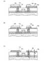
(実施形態1)
本実施形態は図1を用いて、基板1上にトップゲート型のTFTを形成する方法を説
明する。基板1は透光性を有する基板、例えば石英基板、ガラス基板またはプラスチック
基板である。なお、基板1は遮光性の基板でもよく、半導体基板、SOI(Silico
n on Insulator)基板でもよい。(Embodiment 1)
In this embodiment, a method of forming a top gate type TFT on a
n on Insulator) substrate.
基板1上に下地膜として絶縁膜2を成膜する。絶縁膜2としては、酸化シリコン膜、
窒化シリコン膜または酸化窒化シリコン膜(SiOxNy)等の絶縁膜の単層、或いはこ
れらの膜の少なくとも2つの膜でなる積層を用いる。次いで、絶縁膜2上に島状半導体膜
3を形成する。An
A single layer of an insulating film such as a silicon nitride film or a silicon oxynitride film (SiOx Ny ) or a stack of at least two of these films is used. Next, an island-
島状半導体膜3は、絶縁膜2上にスパッタ法、LPCVD法、またはプラズマCVD
法等により半導体膜を全面に形成した後、フォトリソグラフィ法等により形成されたマス
クを用いて半導体膜を形状加工して形成する。島状半導体膜3を結晶性半導体膜で形成す
るときは、基板1上に直接結晶性半導体膜を形成する方法と、非晶質半導体膜を基板1上
に形成した後に、加熱処理により結晶化させて結晶性半導体膜を形成する方法がある。後
者の方法において、結晶化の際の加熱処理は、加熱炉、レーザ照射、若しくはレーザ光の
代わりにランプから発する光の照射(以下、ランプアニールと表記する)、又はそれらを
組み合わせて用いることにより行われる。The island-
After a semiconductor film is formed over the entire surface by a method or the like, the semiconductor film is formed by shape processing using a mask formed by a photolithography method or the like. When the island-shaped
また、ニッケルなどを非晶質半導体膜に添加した後に上記加熱処理を行う熱結晶化法
により結晶性半導体膜を形成してもよい。なお、ニッケルを用いた熱結晶化法を用いて結
晶化を行って結晶性半導体膜を得た場合は、結晶化後にニッケルを除去するゲッタリング
処理を行うことが好ましい。Alternatively, the crystalline semiconductor film may be formed by a thermal crystallization method in which the heat treatment is performed after nickel or the like is added to the amorphous semiconductor film. Note that in the case where a crystalline semiconductor film is obtained by performing crystallization using a thermal crystallization method using nickel, it is preferable to perform gettering treatment for removing nickel after crystallization.
レーザー照射により結晶化して結晶性半導体膜を作製する場合には、連続発振(CW
:continuous−wave)型のレーザビームやパルス発振型のレーザビーム(
パルスレーザビーム)を用いることができる。ここで用いることができるレーザビームは
、Arレーザ、Krレーザ、エキシマレーザなどの気体レーザ、単結晶のYAG、YVO
4、フォルステライト(Mg2SiO4)、YAlO3、GdVO4、若しくは多結晶(
セラミック)のYAG、Y2O3、YVO4、YAlO3、GdVO4に、ドーパントと
してNd、Yb、Cr、Ti、Ho、Er、Tm、Taのうち1種または複数種添加され
ているものを媒質とするレーザ、ガラスレーザ、ルビーレーザ、アレキサンドライトレー
ザ、Ti:サファイアレーザ、銅蒸気レーザまたは金蒸気レーザのうち一種または複数種
から発振されるものを用いることができる。このようなレーザビームの基本波、及びこれ
らの基本波の第2高調波から第4高調波のレーザビームを照射することで、大粒径の結晶
を得ることができる。例えば、Nd:YVO4レーザ(基本波1064nm)の第2高調
波(532nm)や第3高調波(355nm)を用いることができる。このレーザは、C
Wで射出することも、パルス発振で射出することも可能である。CWで射出する場合は、
レーザのパワー密度は0.01〜100MW/cm2程度(好ましくは0.1〜10MW
/cm2)必要である。そして、走査速度を10〜2000cm/sec程度として照射
する。When a crystalline semiconductor film is produced by crystallization by laser irradiation, continuous oscillation (CW
: Continuous-wave) type laser beam and pulse oscillation type laser beam (
A pulsed laser beam) can be used. Laser beams that can be used here are gas lasers such as Ar laser, Kr laser, and excimer laser, single crystal YAG, and YVO.
4 , forsterite (Mg2 SiO4 ), YAlO3 , GdVO4 , or polycrystalline (
(Ceramics) YAG, Y2 O3 , YVO4 , YAlO3 , GdVO4 with one or more of Nd, Yb, Cr, Ti, Ho, Er, Tm, Ta added as dopants A laser oscillated from one or more of laser, glass laser, ruby laser, alexandrite laser, Ti: sapphire laser, copper vapor laser, or gold vapor laser as a medium can be used. By irradiating the fundamental wave of such a laser beam and the second to fourth harmonic laser beams of these fundamental waves, a crystal having a large grain size can be obtained. For example, a second harmonic (532 nm) or a third harmonic (355 nm) of an Nd: YVO4 laser (fundamental wave 1064 nm) can be used. This laser is C
It is possible to emit with W or with pulse oscillation. When injecting with CW,
The power density of the laser is about 0.01 to 100 MW / cm2 (preferably 0.1 to 10 MW).
/ Cm2 ). Then, irradiation is performed at a scanning speed of about 10 to 2000 cm / sec.
なお、単結晶のYAG、YVO4、フォルステライト(Mg2SiO4)、YAlO
3、GdVO4、若しくは多結晶(セラミック)のYAG、Y2O3、YVO4、YAl
O3、GdVO4に、ドーパントとしてNd、Yb、Cr、Ti、Ho、Er、Tm、T
aのうち1種または複数種添加されているものを媒質とするレーザ、Arイオンレーザ、
またはTi:サファイアレーザは、連続発振をさせることが可能であり、Qスイッチ動作
やモード同期などを行うことによって10MHz以上の発振周波数でパルス発振をさせる
ことも可能である。10MHz以上の発振周波数でレーザビームを発振させると、半導体
膜がレーザビームによって溶融してから固化するまでの間に、次のパルスが半導体膜に照
射される。従って、発振周波数が低いパルスレーザを用いる場合と異なり、半導体膜中に
おいて固液界面を連続的に移動させることができるため、走査方向に向かって連続的に成
長した結晶粒を得ることができる。Single crystal YAG, YVO4 , forsterite (Mg2 SiO4 ), YAlO
3 , GdVO4 , or polycrystalline (ceramic) YAG, Y2 O3 , YVO4 , YAl
O3 , GdVO4 and Nd, Yb, Cr, Ti, Ho, Er, Tm, T as dopants
a laser, Ar ion laser, using one or more of a added as a medium,
Alternatively, the Ti: sapphire laser can oscillate continuously, and can oscillate in a pulse at an oscillation frequency of 10 MHz or more by performing Q switch operation, mode synchronization, or the like. When the laser beam is oscillated at an oscillation frequency of 10 MHz or more, the semiconductor film is irradiated with the next pulse during the period from when the semiconductor film is melted by the laser beam to solidification. Therefore, unlike the case of using a pulse laser having a low oscillation frequency, the solid-liquid interface can be continuously moved in the semiconductor film, so that crystal grains continuously grown in the scanning direction can be obtained.
媒質としてセラミック(多結晶)を用いると、短時間かつ低コストで自由な形状に媒
質を形成することが可能である。単結晶を用いる場合、通常、直径数mm、長さ数十mm
の円柱状の媒質が用いられているが、セラミックを用いる場合はさらに大きいものを作る
ことが可能である。When ceramic (polycrystal) is used as the medium, it is possible to form the medium in a free shape in a short time and at low cost. When using a single crystal, it is usually several mm in diameter and several tens of mm
The cylindrical medium is used, but when ceramic is used, a larger one can be made.
発光に直接寄与する媒質中のNd、Ybなどのドーパントの濃度は、単結晶中でも多
結晶中でも大きくは変えられないため、濃度を増加させることによるレーザの出力向上に
はある程度限界がある。しかしながら、セラミックの場合、単結晶と比較して媒質の大き
さを著しく大きくすることができるため大幅な出力向上が実現できる。Since the concentration of dopants such as Nd and Yb in the medium that directly contributes to light emission cannot be changed greatly regardless of whether it is a single crystal or a polycrystal, there is a certain limit to improving the laser output by increasing the concentration. However, in the case of ceramic, since the size of the medium can be remarkably increased as compared with the single crystal, a significant output improvement can be realized.
さらに、セラミックの場合では、平行六面体形状や直方体形状の媒質を容易に形成す
ることが可能である。このような形状の媒質を用いて、発振光を媒質の内部でジグザグに
進行させると、発振光路を長くとることができる。そのため、増幅が大きくなり、大出力
で発振させることが可能になる。また、このような形状の媒質から射出されるレーザビー
ムは射出時の断面形状が四角形状であるため、丸状のビームと比較すると、線状ビームに
整形するのに有利である。このように射出されたレーザビームを、光学系を用いて整形す
ることによって、短辺の長さ1mm以下、長辺の長さ数mm〜数mの線状ビームを容易に
得ることが可能となる。また、励起光を媒質に均一に照射することにより、線状ビームは
長辺方向にエネルギー分布の均一なものとなる。Further, in the case of ceramic, a medium having a parallelepiped shape or a rectangular parallelepiped shape can be easily formed. When a medium having such a shape is used to cause oscillation light to travel in a zigzag manner inside the medium, the oscillation optical path can be made longer. As a result, amplification is increased and oscillation can be performed with high output. Further, since the laser beam emitted from the medium having such a shape has a quadrangular cross-sectional shape at the time of emission, it is advantageous for shaping into a linear beam as compared with a round beam. By shaping the emitted laser beam using an optical system, it is possible to easily obtain a linear beam having a short side length of 1 mm or less and a long side length of several mm to several m. Become. Further, by irradiating the medium with excitation light uniformly, the linear beam has a uniform energy distribution in the long side direction.
この線状ビームを半導体膜に照射することによって、半導体膜の全面をより均一にア
ニールすることが可能になる。線状ビームの両端まで均一なアニールが必要な場合は、そ
の両端にスリットを配置し、エネルギーの減衰部を遮光するなどの工夫が必要となる。By irradiating the semiconductor film with this linear beam, the entire surface of the semiconductor film can be annealed more uniformly. When uniform annealing is required up to both ends of the linear beam, it is necessary to arrange a slit at both ends to shield the energy attenuating portion.
このようにして得られた強度が均一な線状ビームを用いて半導体膜をアニールし、こ
の半導体膜を用いて電子機器を作製すると、その電子機器の特性は、良好かつ均一である
。When a semiconductor film is annealed using a linear beam having a uniform intensity obtained in this manner and an electronic device is manufactured using this semiconductor film, the characteristics of the electronic device are good and uniform.
次いで、必要があればTFTのしきい値を制御するために微量な不純物元素(ボロン
またはリン)のドーピングを半導体膜に対して行う。ここでは、質量分離しないでプラズ
マ励起したイオンドープ法を用いる。Next, if necessary, a small amount of impurity element (boron or phosphorus) is doped into the semiconductor film in order to control the threshold value of the TFT. Here, an ion doping method that is plasma-excited without mass separation is used.
島状半導体膜3の厚さは25〜80nm(好ましくは30〜70nm)の厚さで形成
する。半導体膜の材料に限定はないが、好ましくはシリコンまたはシリコンゲルマニウム
(SiGe)合金などで形成すると良い。The island-
そして、島状半導体膜3を覆うようにゲート絶縁膜4を形成する。ゲート絶縁膜4と
しては、熱酸化膜、酸化シリコン膜、窒化シリコン膜または酸化窒化シリコン膜などの単
層または積層構造を用いることができる。島状半導体膜3と接するゲート絶縁膜4は酸化
珪素膜が好ましい。それは、ゲート絶縁膜4を酸化珪素膜にすると島状半導体膜との界面
におけるトラップ準位が少なくなるからである。また、ゲート電極をMoで形成するとき
は、ゲート電極と接するゲート絶縁膜は窒化シリコン膜が好ましい。それは、窒化シリコ
ン膜はMoを酸化させないからである。Then, a
ここではゲート絶縁膜4として、プラズマCVD法により厚さ115nmの酸化窒化
シリコン膜(組成比Si=32%、O=59%、N=7%、H=2%)を形成する。Here, a 115 nm thick silicon oxynitride film (composition ratio Si = 32%, O = 59%, N = 7%, H = 2%) is formed as the
次に、ゲート絶縁膜4上に導電層を形成して、フォトリソグラフィ法等により形成し
たマスクを用いて導電層を形状加工し、ゲート電極5を形成する。ゲート電極材料として
はMo、Ti、W、Al、Nd、Cr、これら元素の合金等がある。もしくは、これら元
素またはこれら元素の合金の積層によりゲート電極5を構成しても良い。ここではMoに
よりゲート電極を形成する。次に、ゲート電極5またはレジストをマスクとして島状半導
体膜3に不純物元素をドーピングし、チャネル形成領域8と、ソース領域及びドレイン領
域となる不純物領域9とを形成する。Next, a conductive layer is formed over the
その後、窒化珪素を用いて第1層間絶縁膜6を形成する。そして、島状半導体膜3に
添加された不純物元素の活性化および水素化を行う。なお、第1層間絶縁膜6は形成しな
くとも良い。Thereafter, a first interlayer insulating film 6 is formed using silicon nitride. Then, the impurity element added to the island-
次いで、透光性を有する無機材料(酸化シリコン、窒化シリコン、酸化窒化シリコン
など)または、低誘電率の有機化合物材料(感光性又は非感光性の有機樹脂材料)を用い
て第2層間絶縁膜7を形成する。また、シロキサンを含む材料を用いて第2層間絶縁膜を
形成してもよい。なお、シロキサンは、シリコン(Si)と酸素(O)との結合で骨格構
造が構成される材料である。置換基として、少なくとも水素を含む有機基(例えばアルキ
ル基、芳香族炭化水素)が用いられる。置換基としてフルオロ基を用いてもよい。または
置換基として、少なくとも水素を含む有機基と、フルオロ基とを用いてもよい。第2層間
絶縁膜7は積層構造でも良い。Next, the second interlayer insulating film is formed using a light-transmitting inorganic material (silicon oxide, silicon nitride, silicon oxynitride, or the like) or a low dielectric constant organic compound material (photosensitive or non-photosensitive organic resin material). 7 is formed. Alternatively, the second interlayer insulating film may be formed using a material containing siloxane. Siloxane is a material in which a skeleton structure is formed by a bond of silicon (Si) and oxygen (O). As a substituent, an organic group containing at least hydrogen (for example, an alkyl group or an aromatic hydrocarbon) is used. A fluoro group may be used as a substituent. Alternatively, an organic group containing at least hydrogen and a fluoro group may be used as a substituent. The second
次いで、フォトマスクを用いてレジストからなるマスクを形成し、そのマスクを用い
て、第1層間絶縁膜6、第2層間絶縁膜7、及びゲート絶縁膜4を選択的にエッチングし
、コンタクトホールを形成する。そして、レジストからなるマスクを除去する。Next, a resist mask is formed using a photomask, and the first interlayer insulating film 6, the second
そして、第2層間絶縁膜7上にスパッタ法または印刷法で導電膜を形成する。導電膜
は透明導電膜であっても反射性を有していても良い。透明導電膜である場合は、例えば、
酸化インジウムに酸化スズを混ぜたインジウムスズ酸化物(ITO)膜、インジウムスズ
酸化物(ITO)に酸化珪素を混ぜたインジウムスズ珪素酸化物(ITSO)膜、酸化イ
ンジウムに酸化亜鉛を混ぜたインジウム亜鉛酸化物(IZO)膜、酸化亜鉛膜、または酸
化スズ膜を用いることができる。なお、IZOとは、ITOに2〜20wt%の酸化亜鉛
(ZnO)を混合させたターゲットを用いてスパッタリングにより形成される透明導電材
料である。Then, a conductive film is formed on the second
Indium tin oxide (ITO) film in which tin oxide is mixed with indium oxide, Indium tin silicon oxide (ITSO) film in which indium tin oxide (ITO) is mixed with silicon oxide, Indium zinc in which indium oxide is mixed with zinc oxide An oxide (IZO) film, a zinc oxide film, or a tin oxide film can be used. Note that IZO is a transparent conductive material formed by sputtering using a target in which 2 to 20 wt% of zinc oxide (ZnO) is mixed with ITO.
第2層間絶縁膜7上に透明導電膜10を形成し、続いて透明導電膜10上に金属膜1
1を積層する。透明導電膜10と金属膜11は連続的にスパッタで形成することができる
。A transparent
1 is laminated. The transparent
透明導電膜は抵抗の高い材料が多いため、金属膜11は、透明導電膜よりも抵抗の低
い材料が好ましい。例えば、Ti、Mo、Ta、Cr、W、Alなどを用いることができ
る。また、Ti、Mo、Ta、Cr、WのいずれかとAlとを積層させた2層構造、Al
をTi、Mo、Ta、Cr、Wなどの金属で挟んだ3層積層構造としても良い。次いで、
金属膜11上にレジスト膜を全面に塗布した後、図1(A)に示す露光マスクを用いて露
光を行う。Since the transparent conductive film has many materials having high resistance, the
It is good also as a 3 layer laminated structure which pinched | interposed between metals, such as Ti, Mo, Ta, Cr, and W. Then
After a resist film is applied over the entire surface of the
透明導電膜としてITO膜を用いる場合は、ITO膜を熱処理して結晶化する工程が
必要になってくる。そのときはITO膜をスパッタで形成し、焼成後、金属膜11を形成
すると良い。ITSO膜を用いると、結晶化する工程が不要なため工程が少なくてすむ。In the case where an ITO film is used as the transparent conductive film, a process for crystallizing the ITO film by heat treatment becomes necessary. In that case, an ITO film may be formed by sputtering, and the
図1(A)において、露光マスクは、露光光が遮光される遮光部12a、12bと、
露光光が一部通過する半透部13を有する。半透部13には半透膜19が設けられ、露光
光の光強度を低減させている。遮光部12a、12bは半透膜19上に金属膜20が積層
されて構成されている。遮光部12bの幅はt1、半透部13の幅はt2と示す。ここで
は半透部に半透膜を用いた例を示したが、これに限定されず、半透部は露光光の光強度を
低減するものであればよい。また、半透部に回折格子パターンを用いてもよい。In FIG. 1A, the exposure mask includes light shielding portions 12a and 12b for shielding exposure light,
It has a semi-transmissive portion 13 through which a part of the exposure light passes. The semi-transmissive portion 13 is provided with a
図1(A)に示す露光マスクを用いてレジスト膜の露光を行うと、レジスト膜に非露
光領域14aと露光領域14bが形成される。露光時には、光が遮光部12a、12bで
回り込んだり、半透部13を通過することによって図1(A)に示す露光領域14bが形
成される。When the resist film is exposed using the exposure mask shown in FIG. 1A, a
そして、現像を行うと、露光領域14bが除去されて、図1(B)に示すように、大
きく分けて2つの膜厚を有するレジストパターン15aと、膜厚がほぼ一様なレジストパ
ターン16aが金属膜11上に得られる。レジストパターン15aは膜厚の厚い領域と、
該領域より膜厚の薄い領域とを有し、膜厚の薄い領域については、露光エネルギーまたは
半透膜19の透過率を調節することで膜厚を調節することができる。レジストパターン1
5aは左右非対称であり、レジストパターン16aは左右対称である。When the development is performed, the exposed
The thickness of the thin film region can be adjusted by adjusting the exposure energy or the transmittance of the
5a is asymmetrical and the resist
次に、ドライエッチングにより金属膜11及び透明導電膜10のエッチングを行う。
ドライエッチングはECR(Electron Cycrotron Resonanc
e)やICP(Inductive Coupled Plasma)などの高密度プラ
ズマ源を用いたドライエッチング装置によって行われる。Next, the
Dry etching is ECR (Electron Cyctron Resonance).
e) or a dry etching apparatus using a high-density plasma source such as ICP (Inductive Coupled Plasma).
なお、ここでは、ICP型エッチング装置を用いた例を示すが、これに限定されず、
例えば、平行平板型エッチング装置、マグネトロン型エッチング装置、ECR型エッチン
グ装置、ヘリコン型エッチング装置を用いてもよい。In addition, although the example using an ICP type etching apparatus is shown here, it is not limited to this,
For example, a parallel plate etching apparatus, a magnetron etching apparatus, an ECR etching apparatus, or a helicon etching apparatus may be used.
金属膜11及び透明導電膜10のエッチングをウェットエッチングにより行っても良
い。但し、微細加工にはドライエッチングが適しているため、ドライエッチングが好まし
い。また、金属膜11及び透明導電膜10と、第2層間絶縁膜7との材料が異なるため、
ドライエッチングで行っても、第2層間絶縁膜7は金属膜11及び透明導電膜10に対し
て大きなエッチング選択比がとれる。さらにエッチング選択比を大きくするため、第2層
間絶縁膜7の少なくとも最上層を窒化珪素膜で形成しても良い。Etching of the
Even when dry etching is performed, the second
こうして、図1(C)で示すように、第2層間絶縁膜7上に、透明導電膜17aと金
属膜17bとの積層で構成されるパターンと、透明導電膜18aと金属膜18bとの積層
で構成されるパターンが形成される。Thus, as shown in FIG. 1C, on the second
次に、レジストパターン15a、16aをアッシングまたはエッチングする(図2(
A))。この工程により、レジストパターン15aの膜厚の薄い領域がエッチングされる
とともに、その膜厚の薄い領域の膜厚分だけレジストパターン15a、16aの全体の膜
厚も薄くなる。そしてレジストパターン15b、16bを形成する。レジストパターン1
5a、16aは、膜厚方向だけでなく、幅方向もエッチングされるため、レジストパター
ン15b、16bの幅は金属膜17b及び18b、透明導電膜17a、18aの幅よりも
小さくなる。したがって、レジストパターン15b、16bの側面は下層にある金属膜及
び透明導電膜の側面と一致せず、レジストパターン15b、16bの側面の方が後退して
いる。図2(B)では、レジストパターン15bは左右非対称であり、レジストパターン
16bは左右対称である。Next, the resist
A)). By this step, the thin region of the resist
Since 5a and 16a are etched not only in the film thickness direction but also in the width direction, the widths of the resist
次に、レジストパターン15bを用いて金属膜18bをエッチングし、金属膜18c
を形成する(図2(B))。このときに透明導電膜18aが無用にエッチングされないよ
うに、金属膜18bの材料は透明導電膜18aに対し高い選択比がとれるものが好ましい
。例えば、透明導電膜18aの材料がITSOであれば、金属膜18bの材料としてTi
、Mo、Cr、Al等が好ましく、金属膜18bはこれら材料でなる積層構造であっても
良い。そして透明導電膜18aよりもパターンの小さい、つまり平面面積の小さい金属膜
18cを形成する。一方、金属膜17bもレジストパターン16bを用いてエッチングさ
れ、透明導電膜17aよりも平面面積の小さい金属膜17cが形成される。Next, the
Is formed (FIG. 2B). At this time, it is preferable that the material of the
Mo, Cr, Al, etc. are preferable, and the
図2(A)から図2(B)の金属膜17b及び18bのエッチングは、ドライエッチ
ングで行ってもウェットエッチングで行っても良いが、図2(B)ではドライエッチング
により金属膜17c及び18cを形成した場合を図示する。ドライエッチングで行った場
合は金属膜18cの断面における側面は非対称となる。なぜならレジストパターン15b
の形状が非対称なため、その形状を反映した金属膜18cが形成されるからである。金属
膜18cは、一方の側面よりも他方の側面がより傾斜が大きい断面形状となる。金属膜1
7cは、側面がレジストパターン16bの側面と一致するように形成される。金属膜18
cは、一方の側面はレジストパターン15bの一方の側面の延長線上にあり、他方の側面
はレジストパターン15bの他方の側面と一致する。The etching of the
This is because the
7c is formed such that the side surface coincides with the side surface of the resist
In c, one side surface is on an extension line of one side surface of the resist
金属膜17b及び18bをウェットエッチングすると、等方的にエッチングが進むた
め、レジストパターン15b、16bよりも小さい金属膜が形成される。図4にウェット
エッチングを行った場合の図を示す。図4(A)では、金属膜17b及び18bをそれぞ
れウェットエッチングして、金属膜17d及び18dを形成している。その他は図2(B
)と同様である。When the
).
レジストパターン15b、16bの側面と金属膜17d、18dの側面は一致しない
。故に、同一のレジストパターン15b、16bをマスクとしても、ドライエッチングよ
りウェットエッチングで形成したほうが、より小さい金属膜17d及び18dが形成され
る。The side surfaces of the resist
図4(B)は金属膜17dが3層の積層で形成されている場合の図である。例えば金
属膜17dはTi膜91a、93aとでアルミニウム膜92aを挟んだ積層構造であり、
金属膜17dとレジストパターン16bとの側面は一致していない。また、金属膜18d
もTi膜91b、93bとでアルミニウム膜92bを挟んだ積層構造であり、金属膜18
dとレジストパターン15bとの側面は一致していない。FIG. 4B is a diagram in the case where the
The side surfaces of the
Also, the
The side surfaces of d and the resist
図4(A)、(B)において、透明導電膜17a、18aはドライエッチングで形成
されるため、その側面は、基板面に対してほぼ垂直または90度に近い角度θ1を有する
。一方、金属膜17d、18dがウェットエッチングで形成されると、等方的なエッチン
グにより、その側面は、基板面に対して鋭角な角度θ2を有する。したがって、透明導電
膜の側面の角度θ1と金属膜の側面の角度θ2を比較すると、θ1>θ2となっている。
なお、角度θ1とは基板1の表面に対して透明導電膜側面の傾斜角度であり、角度θ2と
は基板1の表面に対して金属膜の側面の傾斜角であり、θ1、θ2ともに0°〜90°の
範囲内である。In FIG. 4 (A), (B) , the transparent
Note that the angle θ1 is the inclination angle of the side surface of the transparent conductive film with respect to the surface of the
金属膜が図4(B)のように積層構造の場合は、各層によってエッチング速度が異な
るときがある。これに伴い、基板面に対して各層の側面がなす角度もそれぞれ異なるとき
がある。したがって金属膜が積層であるときは、基板面に対して最下層の膜の側面がなす
角度をθ2とする。In the case where the metal film has a stacked structure as shown in FIG. 4B, the etching rate may be different depending on each layer. Along with this, the angles formed by the side surfaces of the respective layers with respect to the substrate surface may be different. Therefore, when the metal film is laminated, the angle formed by the side surface of the lowermost film with respect to the substrate surface is θ2 .
なお、金属膜17d、18d及び透明導電膜である透明導電膜17a、18aの側面
がなだらかな面とならずに、凸凹を持つ場合がある。その場合、角度θ1及び角度θ2は
適宜決定すればよい。例えば、凸凹した側面に対し大まかな直線または曲線を引き、それ
を用いて角度θ1及び角度θ2を決定することができる。また、凸凹した側面に基づき、
複数の角度θ1及び角度θ2をとって、その平均値を角度θ1及び角度θ2とすることが
できる。最も合理的な方法を用いれば良い。Note that the side surfaces of the
A plurality of angles θ1 and θ2 can be taken, and the average values can be taken as angles θ1 and θ2 . The most reasonable method should be used.
以上より、ドライエッチング法またはウェットエッチング法のいずれかのエッチング
方法で金属膜17c及び18cまたは金属膜17d及び18dを形成する。どちらのエッ
チング法で形成しても、透明導電膜17a及び18aの側面よりも後退した側面を有する
金属膜17c及び金属膜18cまたは金属膜17d及び18dが形成される。つまり、透
明導電膜17aよりも平面面積が小さい金属膜17cまたは金属膜17d、及び透明導電
膜18aよりも平面面積の小さい金属膜18cまたは18dが形成される。その要因の一
つは、透明導電膜17a、18aを形成するためのマスクであるレジストパターン15a
、16aと、金属膜を形成するためのマスクであるレジストパターン15b、16bの大
きさが異なり、レジストパターン15b、16bのほうが小さいからである。As described above, the
16a and resist
その後、レジストパターン15b、16bを除去する(図2(C))。そして透明導
電膜17a及び金属膜17cでなる配線または電極、透明導電膜18a及び金属膜18c
でなる配線または電極が形成される。透明導電膜18aは画素電極として機能する。図4
(A)及び(B)からレジストパターン15b、16bを除去すれば、透明導電膜17a
及び金属膜17dでなる配線または電極、透明導電膜18a及び金属膜18dでなる配線
または電極が形成される。Thereafter, the resist
A wiring or an electrode is formed. The transparent
If the resist
Then, a wiring or electrode made of the
レジストパターン15bをマスクとして金属膜18bをエッチングをするときに、透
明導電膜18a表面の一部は多少エッチングされる。特に、ドライエッチングにより金属
膜18cを形成するときは、下層の透明導電膜と選択比がとりにくいので、より透明導電
膜18a表面の一部はエッチングされやすい。そのため、図2(C)の透明導電膜18a
の膜厚aと、膜厚bを比較すると、膜厚a<膜厚bとなる。なお、膜厚aとは金属膜18
cまたは金属膜18dと重ならない部分における透明導電膜18aの平均膜厚を言い、膜
厚bとは不純物領域9に達するコンタクトホール底部における透明導電膜18aの膜厚を
言う。When the
When the film thickness a and the film thickness b are compared, the film thickness a <film thickness b. The film thickness a is the
c or the average film thickness of the transparent
図2(C)に示すTFT上に発光素子を積層して、基板1の方向へ発光する発光装置
を形成した場合、透明導電膜18aの膜厚が薄いことで透過率が高くなり、明るい表示を
提供できる。そのため膜厚aは薄い方が好ましい。また、レジストパターン15bをマス
クとして金属膜18bをエッチングする際に、透明導電膜18a表面をエッチングできる
ため、表面のゴミを除去することができ、ゴミに起因する発光素子の短絡を防ぐことがで
きる。In the case where a light-emitting element is stacked over the TFT illustrated in FIG. 2C and a light-emitting device that emits light in the direction of the
本実施形態で形成する金属膜18cは、一方の側面が傾斜している。そのため、液晶
表示装置に利用した場合、金属膜18cの傾斜している側面側からラビングするようにす
ると、金属膜18cの側面においてスムーズにラビングを行うことができる。金属膜18
cの側面が垂直である方向からラビングを行うと、垂直な側面部分でラビング布にストレ
スがかかる等の理由でラビングが不完全になり、配向が不完全になることがあった。した
がって、ラビングは金属膜18cの側面が傾斜している側から行うことが好ましい。One side surface of the
When rubbing is performed from the direction in which the side surface of c is vertical, rubbing may be incomplete due to stress applied to the rubbing cloth at the vertical side surface portion, and alignment may be incomplete. Therefore, rubbing is preferably performed from the side where the side surface of the
また、図4に示すようにウェットエッチングにより、両側面ともに傾斜している金属
膜17d及び18dを形成する場合は、どちらの方向からもスムーズにラビングでき、よ
り効果的である。Further, when the
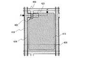
図3に図2(C)の上面図を示す。図2(C)は図3のA−A´における断面図であ
る。図3から分かるように、透明導電膜17a及び金属膜17cの積層でなる配線または
電極は、TFTのソース電極またはドレイン電極として機能し、さらにソース配線として
も機能する。また、透明導電膜18a及び金属膜18cでなる配線または電極は、TFT
のソース電極またはドレイン電極として機能し、さらに画素電極としても機能する。厳密
には、金属膜18cと重ならない透明導電膜18aの部分が画素電極として機能し、光を
通す部分である。また、容量配線21はゲート電極5と同一層から形成されており、容量
配線21は透明導電膜18aと重なることで、容量を形成する。なお、容量配線21はゲ
ート電極5と異なる層で形成しても良い。金属膜17cの側面は透明導電膜17aの側面
と一致せず、透明導電膜17aの側面の内側に位置する。金属膜18cの側面は透明導電
膜18aの側面と一致せず、透明導電膜18aの側面の内側に位置する。図4で説明した
金属膜17dと透明導電膜17aの関係、金属膜18dと透明導電膜18aの関係も同様
である。FIG. 3 shows a top view of FIG. FIG. 2C is a cross-sectional view taken along the line AA ′ of FIG. As can be seen from FIG. 3, the wiring or electrode formed by laminating the transparent
It functions as a source electrode or a drain electrode, and also functions as a pixel electrode. Strictly speaking, a portion of the transparent
本実施形態において、画素電極として機能する透明導電膜を平坦な面上に形成するこ
とは、透明導電膜の断切れを防ぐ意味で非常に有益である。金属膜18cをエッチングに
より形成するときに、金属膜18cから露出する下層の透明導電膜18aの表面も多少エ
ッチングされる。そのため透明導電膜18aが段差のある面上に形成されることで透明導
電膜の膜厚が不均一であると、金属膜18cを形成するエッチングにより、膜厚の薄い透
明導電膜部分がエッチングされ、透明導電膜が断切れを起こす可能性がある。断切れが起
こると、断切れした部分で光漏れが生じたり、画素電極の面積が小さくなり開口率が低く
なったりする。よって、金属膜18cから露出する透明導電膜18aの部分を平坦な面上
に形成するのが好ましい。そのためには、第2層間絶縁膜7を有機材料で形成し、平坦面
を有する第2層間絶縁膜を形成するのが好適である。In the present embodiment, it is very beneficial to form a transparent conductive film functioning as a pixel electrode on a flat surface in order to prevent the transparent conductive film from being cut off. When the
本発明により金属膜と導電膜の積層を形成すると、金属膜の下に接して導電膜が位置
する構成となる。しかし段差が大きい部分では必ずしも金属膜の下に接して導電膜が位置
するとは限らない。それは、段差により導電膜が断切れしてしまう可能性があるからであ
る。従って、図1の不純物領域9に達するコンタクトホールの部分では、導電膜上に金属
膜を配置するのが良い。When a laminate of a metal film and a conductive film is formed according to the present invention, the conductive film is positioned in contact with the metal film. However, the conductive film is not necessarily located in contact with the metal film at the portion where the level difference is large. This is because there is a possibility that the conductive film is cut off by the step. Therefore, it is preferable to dispose a metal film on the conductive film in the contact hole portion reaching the impurity region 9 in FIG.
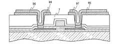
図19にコンタクトホールで導電膜が断切れしている状態を示す。コンタクトホール
側面の傾斜により、導電膜94、95が部分的に切れた状態になっている。しかし、コン
タクトホール部で導電膜94、95上に金属膜96、97が形成されるようにすれば、透
明導電膜が切れたとしても、金属膜を介して切れた導電膜同士を電気的に接続することが
できる。この場合、コンタクトホールの側面では金属膜96、97は第2層間絶縁膜7に
接している部分がある。また、コンタクトホール部分の導電膜は画素電極としては機能し
ないため、上部に金属膜を残存させても全く問題ない。よって、本実施形態の構成では、
透明導電膜がコンタクトホールで断切れしたとしても、上部に形成される金属膜で透明導
電膜の電気的接続を補うことができ、表示欠陥を防ぐことができる。FIG. 19 shows a state where the conductive film is cut off at the contact hole. Due to the inclination of the side surface of the contact hole, the
Even if the transparent conductive film is cut off at the contact hole, the metal film formed on the top can supplement the electrical connection of the transparent conductive film, and display defects can be prevented.
また、図3の容量配線21に起因して導電膜に段差がある部分にも、導電膜上に金属
膜を残存させるのが良い。段差により導電膜が切れたとしても、金属膜を介して導電膜同
士を電気的に接続することができるため、確実に容量を形成することが可能となる。Further, it is preferable that the metal film be left on the conductive film even in a portion where the conductive film has a step due to the
なお、図3における透明導電膜18aの形状は一例であり、他の形状でも良い。例え
ば、櫛歯状の縁を持たせることでIPS(In−Plane−Switching)方式
、FFS(Fringe Field Switching)方式に用いる画素電極にし
たり、スリットをいれることでMVA(Multi−domain Vertical
Alignment)方式、PVA(Patterned Vertical Alig
nment)方式に用いる画素電極にすることができる。The shape of the transparent
Alignment method, PVA (Patterned Vertical Align)
pixel electrode used for the “nment” method.
以上より、透明導電膜と金属膜を1つのレジストパターンを用いて形成できるため作
製工程数を減らすことができる。また、透明導電膜を配線または電極として利用しながら
も、金属膜を積層させることで低抵抗にし、導電性を高くすることができる。As described above, since the transparent conductive film and the metal film can be formed using one resist pattern, the number of manufacturing steps can be reduced. In addition, while using a transparent conductive film as a wiring or an electrode, by laminating a metal film, the resistance can be reduced and the conductivity can be increased.
図1(B)に示す状態から透明導電膜10及び金属膜11をエッチングする間に、自
然とレジストパターン15a、16aもエッチングされ、レジストパターン15b、16
bになる場合は、レジストパターンをアッシングまたはエッチングしてレジストパターン
15b、16bを形成する工程は設けなくても良い。While the transparent
In the case of b, the step of forming the resist
なお、本実施形態では結晶性半導体膜でなる島状半導体膜を有するトップゲート型T
FTを用いて説明したが、本実施形態は結晶性半導体膜でなるボトムゲート型TFTにも
応用できる。また、本実施形態では、島状半導体膜はソース領域及びドレイン領域となる
不純物領域9とチャネル形成領域8を有するが、その他にも低濃度不純物領域、オフセッ
ト領域等を有することができる。In this embodiment, a top gate type T having an island-like semiconductor film made of a crystalline semiconductor film.
Although described using FT, this embodiment can also be applied to a bottom-gate TFT made of a crystalline semiconductor film. In this embodiment, the island-shaped semiconductor film has the impurity region 9 and the channel formation region 8 which become the source region and the drain region, but can also have a low concentration impurity region, an offset region, and the like.
(実施形態2)
本実施形態を図5を用いて説明する。本実施形態で説明するTFTを構成する基板の
種類、各層の形成方法及び材料等は実施形態1を参照できる。(Embodiment 2)
This embodiment will be described with reference to FIG.
基板401上に下地膜として絶縁膜402を形成する。なお、下地膜は設けなくても
よい。次に、絶縁膜402上に導電層を形成し、フォトリソグラフィ法等により形成され
たマスクを用いて導電層を形状加工し、ゲート電極403を形成する。An insulating
ゲート電極403を覆うようにゲート絶縁膜404を形成する。ゲート絶縁膜404
上に非晶質半導体膜を形成する。非晶質半導体膜の材料に限定はないが、好ましくはシリ
コンまたはシリコンゲルマニウム(SiGe)合金などで形成すると良い。続いて、非晶
質半導体膜上に導電層を形成する。導電層には例えばリンを含む非晶質シリコン膜を用い
ることができる。そして、フォトリソグラフィ法等により形成されたマスクを用いて、非
晶質半導体膜及び導電層の形状を加工して、島状半導体膜405と導電層406を形成す
る。A
An amorphous semiconductor film is formed thereon. There is no limitation on the material of the amorphous semiconductor film, but it is preferably formed of silicon or a silicon germanium (SiGe) alloy. Subsequently, a conductive layer is formed over the amorphous semiconductor film. For example, an amorphous silicon film containing phosphorus can be used for the conductive layer. Then, the island-shaped
導電層406上に透明導電膜407及び金属膜408を積層形成する。なお、透明導
電膜に代えて反射性を持つ導電層を用いてもよい。また、透明導電膜としては実施形態1
で示した透明導電膜材料を用いることができる。次いで、金属膜408上全面にレジスト
膜を塗布した後、図5(A)に示す露光マスクを用いて露光を行う。A transparent
The transparent conductive film material shown by can be used. Next, after a resist film is applied over the entire surface of the
図5(A)において、露光マスクは、遮光部409a、409b、半透部410を有
する。半透部410には回折パターンまたは半透膜を用いることができる。図5(A)で
示す露光マスクを用いてレジスト膜の露光を行うと、レジスト膜に非露光領域411と露
光領域412が形成される。そして現像を行い、図5(B)に示すように、レジストパタ
ーン413aと414aが形成される。レジストパターン414aは遮光部409bで露
光され、現像された領域422(レジストパターン414aの破線から左側部分)と、半
透部410で露光され、現像された領域423(レジストパターン414aの破線から右
側部分)で構成される。In FIG. 5A, the exposure mask includes
次に、ドライエッチングにより金属膜408及び透明導電膜407のエッチングを行
う。そして、図5(C)で示すように、透明導電膜415及び金属膜416の積層で構成
されるパターンと、透明導電膜419及び金属膜420の積層で構成されるパターンが形
成される。このエッチングをウェットエッチングにより行っても良い。但し、微細加工に
はドライエッチングが適しているため、ドライエッチングが好ましい。また、金属膜40
8及び透明導電膜407と、ゲート絶縁膜404との材料が異なるため、ドライエッチン
グで行っても大きなエッチング選択比がとれる。さらに両者のエッチング選択比を大きく
するため、ゲート絶縁膜404の少なくとも最上層を窒化珪素膜で形成しても良い。Next, the
8 and the transparent
次に、図6(A)のように、レジストパターン413a、414aをアッシングまた
はエッチングする。この工程により、レジストパターン414aの領域423が除去され
る。またこの領域423の膜厚d2だけ、レジストパターン414aの領域422の膜厚
が薄くなり、レジストパターン414bが形成される。レジストパターン413aも膜厚
d2だけアッシングされ、レジストパターン413bが形成される。さらに幅方向もエッ
チングされるため、レジストパターン413b、414bの幅は金属膜416、420、
透明導電膜415、419の幅よりも小さくなる。したがって、レジストパターン413
b、414bの側面は下層にある金属膜及び透明導電膜の側面と一致せず、レジストパタ
ーン413b、414bの側面の方が後退している。また、レジストパターン414bの
両側面が基板面に対してなす角度は互いに異なる。一方、レジストパターン413bは両
側面が基板面に対してなす角度はほぼ同じである。Next, as shown in FIG. 6A, the resist
It becomes smaller than the width of the transparent
The side surfaces of b and 414b do not coincide with the side surfaces of the underlying metal film and transparent conductive film, and the side surfaces of the resist
次に、レジストパターン414bを用いて金属膜416をエッチングして、金属膜4
21を形成する。また、レジストパターン413bを用いて金属膜420をエッチングし
て、金属膜424を形成する。(図6(B))。このとき透明導電膜415は無用にエッ
チングされないようにする。金属膜424、421は、透明導電膜419、415よりも
小さいパターンで形成される。また、透明導電膜415、419をマスクとして、導電層
406をエッチングし、導電層417及び418を形成する。島状半導体膜405の一部
も少しエッチングされる。透明導電膜419の一方の端部と導電層417の一方の端部、
及び透明導電膜415の一方の端部と導電層418の一方の端部はそれぞれ一致する。金
属膜421及び424の形成は同一工程で行われる。Next, the
21 is formed. In addition, the
And one end of the transparent
また、金属膜421、424を形成するためのエッチングと同時に、導電層406を
エッチングしても良い。Further, the
そして、レジストパターン413b、414bを除去し、透明導電膜419及び金属
膜424でなる配線または電極、金属膜421及び透明導電膜415でなる配線または電
極を形成する。透明導電膜415は画素電極として機能する(図6(C))。Then, the resist
導電層417及び418の形成は図5(C)のエッチングと同時にすることも可能だ
が、図6で示すように、金属膜424、421の形成時または形成後に行うほうが好まし
い。なぜなら、図5(C)の段階で島状半導体膜を露出してしまうと、金属膜424、4
21を形成するときに、さらに島状半導体膜がエッチングされてしまう可能性があるため
である。The
This is because the island-shaped semiconductor film may be further etched when forming 21.
図6(B)のエッチングはドライエッチングでも、ウェットエッチングでも良い。ド
ライエッチングで行う場合は、図6(B)、(C)に示すように、金属膜421の断面形
状はレジストパターン414bの形状を反映して左右非対称となる。つまり、金属膜42
1は、一方の側面よりも他方の側面がより傾斜が大きい断面形状となり、一方の側面はレ
ジストパターン414bの一方の側面の延長線上にあり、他方の側面はレジストパターン
414bの他方の側面と一致する。金属膜424は、側面がレジストパターン413bの
側面と一致するように形成される。The etching in FIG. 6B may be dry etching or wet etching. When dry etching is performed, as shown in FIGS. 6B and 6C, the cross-sectional shape of the
1 has a cross-sectional shape in which the other side surface is more inclined than the one side surface, one side surface is on an extension line of one side surface of the resist
金属膜421及び424をウェットエッチングで形成する場合を図8を用いて説明す
る。ドライエッチングで形成した金属膜421、424に代えて、ウェットエッチングで
形成した場合は金属膜425、426とする。The case where the
ウェットエッチングの場合は、図8で示すようにレジストパターン413b、414
bよりも小さい金属膜425及び426が形成され、レジストパターン413b、414
bの側面と金属膜425、426の側面は一致しない。故に、同一のレジストパターン4
13b、414bをマスクとしても、ドライエッチングよりもウェットエッチングで形成
したほうが、より平面面積が小さい金属膜が形成される。また、図4と同様に、ウェット
エッチングで金属膜を形成した場合、透明導電膜415、419の側面における角度θ1
と、金属膜425、426の側面における角度θ2とを比較すると、θ1>θ2となって
いる。なお、角度θ1とは基板401の表面に対して透明導電膜側面の傾斜角度であり、
角度θ2とは基板401の表面に対して金属膜の側面の傾斜角であり、θ1、θ2ともに
0°〜90°の範囲内である。また、金属膜425、426が図4(B)のように積層構
造であるときは、基板面に対して最下層の膜の側面がなす角度をθ2とする。In the case of wet etching, as shown in FIG.
The side surface of b and the side surfaces of the
Even if 13b and 414b are used as a mask, a metal film having a smaller planar area is formed by wet etching rather than dry etching. Similarly to FIG. 4, when the metal film is formed by wet etching, the angle θ1 on the side surface of the transparent
And the angle θ2 on the side surfaces of the
The angle θ2 is the inclination angle of the side surface of the metal film with respect to the surface of the
なお、ウェットエッチングのときは、導電層406のエッチングは、図5(C)での
エッチングと同時でもよいし、図6(B)の金属膜425、426形成した後に行っても
良い。Note that in wet etching, the
いずれのエッチング方法で金属膜を形成しても、側面が透明導電膜419の側面より
も後退した金属膜425または金属膜424、透明導電膜415の側面よりも後退した金
属膜421または金属膜426が形成される。つまり、透明導電膜419よりも平面面積
の小さい金属膜424または425、透明導電膜415よりも平面面積の小さい金属膜4
21または426が形成される。Regardless of which etching method is used to form the metal film, the
21 or 426 is formed.
そして、レジストパターン413b、414bを除去し、透明導電膜419及び金属
膜424でなる配線または電極、金属膜421及び透明導電膜415でなる配線または電
極を形成する(図6(C))。図8からレジストパターン413b、414bを除去すれ
ば、透明導電膜419及び金属膜425でなる配線または電極、透明導電膜415及び金
属膜426でなる配線または電極が形成される。Then, the resist
本発明の膜厚の異なる領域を有するレジストパターン414aを用いて、金属膜42
1及び透明導電膜415の積層を形成すると、金属膜421を形成する際に、透明導電膜
415の表面の一部は多少エッチングされる。特に、ドライエッチングにより金属膜42
1を形成するときは、下層の透明導電膜415と選択比がとりにくいので、より透明導電
膜415表面の一部はエッチングされやすい。そのため、図6(C)の透明導電膜415
の膜厚a(金属膜421から露出する透明導電膜415の膜厚)と、膜厚c(ゲート絶縁
膜404と金属膜421に接する透明導電膜の膜厚)を比較すると、膜厚a<膜厚cとな
る。なお、膜厚aと膜厚cは平均膜厚を言う。The metal film 42 is formed using the resist
1 and the transparent
When 1 is formed, a selective ratio with the lower transparent
When the film thickness a (the film thickness of the transparent
図6(C)のTFT上に発光素子を積層して発光装置を形成すると、膜厚a<膜厚c
であることは次のような効果を奏する。基板401方向へ発光する発光装置ならば、膜厚
aが薄いことで、明るい表示を提供できる。また、透明導電膜415表面をエッチングで
きるため、表面のゴミを除去することができ、発光素子の短絡を防ぐことができる。When a light emitting element is stacked over the TFT in FIG. 6C to form a light emitting device, the film thickness a <film thickness c.
This has the following effects. A light-emitting device that emits light toward the
本実施形態で形成する金属膜421は、一方の側面が傾斜している。そのため、液晶
表示装置に利用した場合、金属膜421の傾斜している側面側からラビングするようにす
ると、金属膜421の側面においてスムーズにラビングを行うことができる。金属膜42
1の側面が垂直である方向からラビングを行うと、垂直な側面部分でラビング布にストレ
スがかかる等の理由でラビングが不完全になり、配向が不完全になることがあった。した
がって、ラビングは金属膜421の側面が傾斜している側から行うことが好ましい。One side surface of the
When rubbing is performed from the direction in which the side surface of 1 is vertical, rubbing may be incomplete due to stress applied to the rubbing cloth at the vertical side surface portion, and alignment may be incomplete. Therefore, rubbing is preferably performed from the side where the side surface of the
また、図8に示すようにウェットエッチングにより、両側面ともに傾斜している金属
膜425及び426を形成する場合は、どちらの方向からもスムーズにラビングでき、よ
り効果的である。Further, when the
図7に図6(C)の上面図を示す。図6(C)は図7のA−A´における断面図であ
る。図7より透明導電膜419と金属膜424の積層でなる配線または電極は、TFTの
ソース電極またはドレイン電極と機能し、さらにソース配線としても機能する。また、透
明導電膜415及び金属膜421でなる配線または電極は、TFTのソース電極またはド
レイン電極として機能し、さらに画素電極としても機能する。厳密には、金属膜421と
重ならない透明導電膜415の部分が画素電極として機能する。また、ゲート電極403
と同層から形成されている容量配線430は、透明導電膜415と重なることで容量を形
成している。なお、ゲート電極とは異なる層から容量配線430を形成してもよい。金属
膜424の側面は透明導電膜419の側面と一致せず、透明導電膜419の側面の内側に
位置する。金属膜421の側面は透明導電膜415の側面と一致せず、透明導電膜415
の側面の内側に位置する。図8で説明した金属膜425と透明導電膜419の関係、金属
膜426と透明導電膜415の関係も同様である。FIG. 7 shows a top view of FIG. FIG. 6C is a cross-sectional view taken along the line AA ′ of FIG. As shown in FIG. 7, the wiring or electrode formed by stacking the transparent
The
Located inside the side. The relationship between the
また、容量配線430、ゲート電極403または島状半導体膜405に起因する段差
上に形成された透明導電膜415を金属膜421により覆うことは、画素電極として機能
する透明導電膜の断切れを防止するため有益である。金属膜421がエッチングにより形
成されるときに透明導電膜415も多少エッチングされるため、透明導電膜の膜厚が一様
でないと、このエッチングの際に透明導電膜が断切れを起こしてしまう。従って、画素電
極として、膜厚が一様に形成されやすい平坦面上の透明導電膜部分を利用するのが好まし
い。そのためには、段差のある面上に位置する透明導電膜415を覆うように、金属膜4
21を形成すればよい。そうすれば、段差のある面上の透明導電膜415はエッチングさ
れず、断切れすることもない。Further, covering the transparent
21 may be formed. Then, the transparent
また、金属膜421で段差面上の透明導電膜415を覆うようにするには、図5(B
)のレジストパターン414aの領域423の膜厚をd2、領域422のうち最も薄い膜
厚をd1としたとき、少なくともd1>d2でなければならない。それは図6(A)のレ
ジストのアッシングのときに、膜厚d2はアッシングされ、レジスト全体の膜厚がd2だ
け薄くなるが、このアッシングにより膜厚がd2だけ薄くなったとしても、領域422に
はレジストが残存している必要があるからである。したがって、少なくともレジストパタ
ーン414aにおいては、領域422の最も膜厚の薄い部分の膜厚d1は、領域423の
膜厚d2よりも厚いことが好ましい。In order to cover the transparent
) Where the film thickness of the
以上の工程により、非晶質半導体膜でなる島状半導体膜を有するボトムゲート型TF
Tを形成できる。透明導電膜を配線または電極として利用しながらも、金属膜を積層させ
ることで低抵抗にし、導電性を高くすることができる。また、金属膜421を形成するた
めのレジストパターンを特別に設ける必要がないので、工程数を減らすことができる。Through the above steps, a bottom gate type TF having an island-shaped semiconductor film made of an amorphous semiconductor film.
T can be formed. While using a transparent conductive film as a wiring or an electrode, by laminating a metal film, the resistance can be lowered and the conductivity can be increased. In addition, since it is not necessary to provide a resist pattern for forming the
なお、本実施形態の別のTFTの構成として、チャネル保護膜を有するTFTの構成
を図9(A)に示す。図9(A)のTFTにおいて、図5〜図8と同じものは同一符号を
付し、詳細な説明は省略する。Note that as another TFT structure of this embodiment mode, a structure of a TFT having a channel protective film is shown in FIG. 9A, the same components as those in FIGS. 5 to 8 are denoted by the same reference numerals, and detailed description thereof is omitted.
基板401上に島状半導体膜405を形成するまでは、図5(A)と同様である。次
に、窒化珪素膜等の絶縁膜を成膜し、エッチングにより該絶縁膜を形状加工して、島状半
導体膜405上の中央付近にチャネル保護膜601を形成する。その後、チャネル保護膜
601を覆うように導電層406、透明導電膜407、金属膜408を順に成膜する。そ
して、金属膜408上全面にレジスト膜を塗布する。そして半透部を有する露光マスクを
用いてレジスト膜を露光した後、現像し、レジストパターン413a、414aを形成す
る。The process until the island-shaped
次に、ドライエッチングにより、レジストパターン413a、414aを用いてエッ
チングし、導電層417、導電層418、透明導電膜415、透明導電膜419、金属膜
416、金属膜420を形成する。透明導電膜415は画素電極として機能する(図9(
B))。チャネル保護膜601は、導電層417及び418を形成する際に、島状半導体
膜405がエッチングされるのを防ぐための保護膜となる。Next, etching is performed by dry etching using the resist
B)). The channel
次に、レジストパターン413a、414aをアッシングして、レジストパターン4
13b、414bを形成する(図9(C))。レジストパターン413b、414bを用
いて、金属膜420、416をエッチングし、金属膜424、421を形成する(図9(
D))。図9(D)はドライエッチングにより金属膜424、421を形成した場合を図
示する。なお、ウェットエッチングにより、図8で示した金属膜425、426を形成し
ても良い。その際の金属膜と透明導電膜の端部の形状は、図8で説明したのと同様である
。Next, the resist
13b and 414b are formed (FIG. 9C). The
D)). FIG. 9D illustrates the case where the
チャネル保護膜601を有する構成のTFTは次のような効果がある。まず、図9(
B)で示す透明導電膜407、金属膜408のエッチング工程でドライエッチングを行っ
たときに、島状半導体膜がエッチングされる心配がない。そのため、透明導電膜及び金属
膜のエッチング工程の自由度があがり、最適なエッチング条件で行うことができる。また
、ドライエッチングにより微細加工が可能となる。さらに、島状半導体膜405を薄く形
成することができ、TFTの特性を向上させることができる。そのため、駆動TFTに大
電流を流すTFTが必要なアクティブマトリクス型有機発光ダイオードには最適である。The TFT having the channel
When dry etching is performed in the etching process of the transparent
また、別のTFTの構成を図10に示す。この構成は結晶性半導体膜で形成されたボ
トムゲート型TFTである。基板401上にゲート絶縁膜404を形成するまでは図5(
A)と同様の工程である。そしてゲート絶縁膜上に結晶性半導体膜を形成する。直接結晶
性半導体膜をゲート絶縁膜上に形成してもよいし、実施形態1のように非晶質半導体膜を
形成後、結晶化して、結晶性半導体膜を形成してもよい。結晶性半導体膜をエッチングに
より形状加工し、島状半導体膜405を形成する。島状半導体膜405に選択的に不純物
をドーピングして、島状半導体膜405に一対の不純物領域602とチャネル形成領域6
03を形成する。島状半導体膜405上に層間絶縁膜604を形成した後、層間絶縁膜6
04に不純物領域602に達するコンタクトホールを形成し、透明導電膜及び透明導電膜
上に金属膜を積層する。そして図5(A)で示した露光マスクで露光され、現像されたレ
ジストパターンを用いてエッチングし、透明導電膜419及び金属膜424でなる電極ま
たは配線、並びに金属膜421及び透明導電膜415でなる電極または配線を形成する。
図10の構成において、層間絶縁膜604を有機樹脂材料等で形成すると、層間絶縁膜6
04が平坦面を有する。つまり透明導電膜415を平坦面に形成することができるので、
金属膜421を形成するエッチングの際に透明導電膜415が断切れするのを防ぐことが
できる。Another TFT structure is shown in FIG. This configuration is a bottom gate TFT formed of a crystalline semiconductor film. Until the
It is the same process as A). Then, a crystalline semiconductor film is formed over the gate insulating film. The crystalline semiconductor film may be formed directly on the gate insulating film, or the amorphous semiconductor film may be formed and crystallized to form the crystalline semiconductor film as in the first embodiment. The crystalline semiconductor film is processed by etching to form an island-shaped
03 is formed. After forming the
A contact hole reaching the
In the configuration of FIG. 10, when the
04 has a flat surface. That is, since the transparent
It is possible to prevent the transparent
なお、図10で示すTFTは一対の不純物領域602以外にも不純物領域を有してい
ても良い。Note that the TFT illustrated in FIG. 10 may include an impurity region in addition to the pair of
また、図9及び図10において、金属膜421、424を形成するためのエッチング
方法に起因する金属膜の形状の特徴は、前述したのと同様である。金属膜421、424
に代えて、ウェットエッチングを用いて図8のような形状の金属膜425、426を形成
することもできるし、積層構造の金属膜を用いてもよい。また、画素電極として機能する
導電膜として透明導電膜を用いたが、反射型の導電膜を用いても構わない。透明導電膜の
材料としては実施形態1で示した材料を用いることができる。9 and 10, the characteristics of the shape of the metal film resulting from the etching method for forming the
Instead, the
本実施形態は、実施可能な範囲で実施形態1と自由に組み合わせることが可能である
。This embodiment can be freely combined with
(実施形態3)
本実施形態では、実施形態1及び2で用いた露光マスクについて図11を用いて説明する
。図11(A)〜(C)は、図1または図5で示した露光マスクの遮光部12b及び半透
部13の上面図を示す。露光マスクの遮光部12bの幅はt1と示し、半透部13の幅は
t2と示している。(Embodiment 3)
In this embodiment, the exposure mask used in
半透部13には回折格子パターンを設けることができ、図11(A)、(B)には露
光装置の解像限界以下の複数のスリットでなるスリット部を有する回折格子パターンが示
されている。回折格子パターンとは、スリット、ドット等のパターンが少なくとも1つ以
上配置されたパターンである。スリット、ドット等のパターンを複数配置する場合は、周
期的に配置されていてもよいし、非周期的に配置されてもよい。解像度限界以下の微細パ
ターンを用いることによって、実質的な露光量を変調することが可能であり、露光された
レジストの現像後の膜厚を調節することが可能である。The semi-transmissive portion 13 can be provided with a diffraction grating pattern, and FIGS. 11A and 11B show a diffraction grating pattern having a slit portion composed of a plurality of slits below the resolution limit of the exposure apparatus. Yes. The diffraction grating pattern is a pattern in which at least one pattern such as a slit and a dot is arranged. When a plurality of patterns such as slits and dots are arranged, they may be arranged periodically or aperiodically. By using a fine pattern below the resolution limit, it is possible to modulate the substantial exposure amount and to adjust the film thickness after development of the exposed resist.
前記スリット部のスリットが延びる方向は、スリット部301の様に遮光部303の
一辺と平行でも、スリット部302の様に遮光部303の一辺と垂直でも構わない。また
は、遮光部303の一辺に対して斜めの方向がスリットの延びる方向でも良い。尚、この
フォトリソグラフィ工程で使用されるレジストはポジ型レジストが好ましい。The direction in which the slit of the slit portion extends may be parallel to one side of the
また、半透部の別の例として、図11(C)に、露光光の光強度を低減する機能を有
する半透膜304を設けた例を示す。半透膜としては、MoSiNの他に、MoSi、M
oSiO、MoSiON、CrSiなどを用いることができる。半透部を備えた露光マス
クを用いた露光法は、ハーフトーン露光法とも呼ばれる。As another example of the semi-transmissive portion, FIG. 11C illustrates an example in which a
oSiO, MoSiON, CrSi, or the like can be used. An exposure method using an exposure mask having a semi-transmissive portion is also called a halftone exposure method.
これら図11(A)〜(C)に示す露光マスクに露光光を照射した場合、遮光部30
3の光強度はゼロであり、透光部305の光強度は100%である。一方、スリット部3
01、302、または半透膜304で構成される光強度低減機能を有する半透部を通過す
る光の強度は、10〜70%の範囲で調整可能となっている。代表的な光強度分布の例を
図11(D)に示す。半透部が回折格子パターンである場合には、半透部を通過する光強
度の調整は、スリット部301、302のピッチ及びスリット幅の調整により実現してい
る。When exposure light is irradiated to the exposure mask shown in FIGS.
The light intensity of 3 is zero, and the light intensity of the
The intensity of light passing through the semi-transmissive portion having the light intensity reducing function constituted by 01, 302 or the
本実施形態は実施形態1、2と自由に組み合わせることができる。 This embodiment can be freely combined with
(実施形態4)
本実施形態ではEL(Electro Luminescence)表示装置を図1
2、13を用いて説明する。TFTを構成する基板や各層の形成方法、材料等については
実施形態1及び2を参照できる。図12、13のTFTは実施形態1のトップゲート型T
FTの構造を用いて説明するが、ボトムゲート型TFT構造でも良い。実施形態1の図1
及び図2と同じものについては同一の符号を付し、詳細な説明を省略する。但し、画素構
成は図12、13に限定されず、他の画素構成でも良い。(Embodiment 4)
In this embodiment, an EL (Electro Luminescence) display device is shown in FIG.
2 and 13 will be used for explanation. Embodiments 1 and 2 can be referred to for the formation method and material of the substrate and each layer constituting the TFT. 12 and 13 is the top gate type T of the first embodiment.
Although described using the FT structure, a bottom-gate TFT structure may be used. FIG. 1 of
The same components as those in FIG. 2 are denoted by the same reference numerals, and detailed description thereof is omitted. However, the pixel configuration is not limited to those shown in FIGS. 12 and 13, and other pixel configurations may be used.
図12(A)にEL表示装置の画素部の上面図を示す。画素には、スイッチング用T
FT140と、EL素子に流れる電流を制御する駆動用TFT141の2つのTFTが設
けられる。スイッチング用TFT140のソース電極またはドレイン電極となる透明導電
膜123及び金属膜124には、駆動用TFT141のゲート電極5bが電気的に接続さ
れている。図12(B)は図12(A)のA−A’及びB−B’における断面図である。FIG. 12A shows a top view of a pixel portion of an EL display device. The pixel has a switching T
Two TFTs, an
基板1上に実施形態1の方法でTFTを形成する。基板1上に絶縁膜2を形成し、そ
の上に島状半導体膜3a、3bを形成する。島状半導体膜3a、3bは非晶質半導体膜ま
たは結晶性半導体膜である。続いて、ゲート絶縁膜4、ゲート電極5a、5bを形成する
。ゲート電極5aはゲート配線から延在してなっており、ゲート電極5bはゲート配線(
ゲート電極5a)とは分離して形成される。ゲート電極5a、5bをマスクとして島状半
導体膜3a、3bに不純物元素をドーピングし、一対の不純物領域とチャネル形成領域を
それぞれの島状半導体膜3a、3bに形成する。次に、ゲート電極5a、5b上に第1層
間絶縁膜6、第2層間絶縁膜7を形成する。A TFT is formed on the
It is formed separately from the
次に、ゲート絶縁膜4、第1層間絶縁膜6及び第2層間絶縁膜7をエッチングし、島
状半導体膜の一対の不純物領域に達するコンタクトホールを形成する。これと同時に、第
1層間絶縁膜6及び第2層間絶縁膜7をエッチングし、ゲート電極5bに達するコンタク
トホールを形成する。第2層間絶縁膜7上に透明導電膜を形成し、さらにその上に金属膜
を積層させる。そして透明導電膜及び金属膜を実施形態1と同様の方法でエッチングし、
金属膜122及び透明導電膜121でなる配線または電極、金属膜124及び透明導電膜
123でなる配線または電極、金属膜126及び透明導電膜125でなる配線または電極
、金属膜128及び透明導電膜127でなる配線または電極を形成する。透明導電膜12
7は画素電極として機能する。Next, the
Wiring or electrode made of
7 functions as a pixel electrode.
金属膜122、124、126は、下層に位置する透明導電膜121、123、12
5とおおよそ相似の関係を有しており、それぞれの透明導電膜よりも一回り小さいパター
ンを有している。金属膜122、124、126を形成するには、図1で示したレジスト
パターン16aのように、遮光部を有する露光マスクで露光、現像されたレジストパター
ンを用いて、エッチングする。一方、透明導電膜127はその一部が画素電極として機能
するため、金属膜128は透明導電膜127と必ずしも相似の関係を持たず、透明導電膜
127よりもより小さいパターンを有する。そのため、透明導電膜127及び金属膜12
8を形成するには、図1で示したレジストパターン15aのように、半透部及び遮光部を
有する露光マスクで露光、現像されたレジストパターンを用いて、エッチングする。The
5 has a similar relationship, and has a pattern slightly smaller than each transparent conductive film. In order to form the
In order to form 8, etching is performed using a resist pattern exposed and developed with an exposure mask having a semi-transmissive portion and a light-shielding portion, like the resist
金属膜122、124、126、128を形成した後、金属膜128から露出してい
る透明導電膜127の部分の表面を研磨して、透明導電膜上の金属膜の残渣を取り除くよ
うにしても良い。研磨はCMP(Chemical−Mechanical Polis
hing)法などで行うことができる。この研磨は、続いて透明導電膜127上に形成さ
れる電界発光層が非常に薄い膜であるので、金属膜の残渣によって電界発光層が均一に成
膜されず、透明導電膜127と電界発光層上の導電層131がショートしてしまうのを防
ぐ効果がある。After forming the
ing) method or the like. In this polishing, since the electroluminescent layer subsequently formed on the transparent
その後、TFT上に土手となる絶縁膜129(隔壁とも言う)を形成する。絶縁膜1
29は透明導電膜127の画素電極として機能する部分を露出するように形成される。ま
た、絶縁膜129は金属膜128を覆うように形成する。これは、金属膜128が絶縁膜
129から露出するとEL素子の短絡不良の原因となるからである。一方で、絶縁膜12
9は、透明導電膜127を露出する付近において、膜厚が連続的に減少し、曲面を持つよ
う形成される。これは、上部に形成される電界発光層が絶縁膜129の段差で断切れしな
いようにするためである。このような絶縁膜129の曲面を持つ形状により、金属膜12
8の端部が絶縁膜129から露出しやすいという懸念があった。しかし、本発明で形成す
る金属膜128は、実施形態1及び2で説明したように、その端部が傾斜している、また
は角度θ2を持つため、絶縁膜129から露出しにくい構成となり、EL表示装置には非
常に好適である。After that, an insulating film 129 (also referred to as a partition wall) is formed over the TFT. Insulating
29 is formed so as to expose a portion of the transparent
9 is formed to have a curved surface in the vicinity where the transparent
There is a concern that the end portion of 8 is easily exposed from the insulating
金属膜128がドライエッチングで形成される場合は、上部に形成されるレジストパ
ターンの形状が反映され、図12(B)の断面図でみると、絶縁膜129の曲面に近い方
の金属膜128の端部がもう一方の端部より傾斜が大きくなる。図12(A)の上面図で
みると、金属膜128の4辺のうち、透明導電膜127の端部とより離れている2辺が、
残りの2辺よりも大きい傾斜を持つ。一方、金属膜128がウェットエッチングで形成さ
れる場合は、透明導電膜127の端部における角度θ1よりも鋭角なθ2を、金属膜12
8の端部は有する。よって、どちらの形成方法であっても、絶縁膜129の曲面に近い金
属膜128の端部は傾斜または角度θ2を持って形成されるため、絶縁膜129から露出
されにくい形状になる。When the
Has a slope greater than the remaining two sides. On the other hand, when the
8 ends have. Therefore, in any of the formation methods, the end portion of the
続いて、絶縁膜129から露出する透明導電膜127に接するように電界発光層13
0を形成し、続いて導電層131を形成する。上記構成では、発光素子を駆動するTFT
がNチャネル型TFTであれば、透明導電膜127が陰極、導電層131が陽極に相当す
る。導電層131に透明導電膜を用いると、上方及び下方の両方に発光する表示装置とな
る。Subsequently, the electroluminescent layer 13 is in contact with the transparent
0 is formed, and then a
If N is an N-channel TFT, the transparent
図13には、図12とは別の構成のEL表示装置を示す。図13(A)にEL表示装
置の画素部の上面図、図13(B)に図13(A)のA−A’及びB−B’における断面
図を示す。FIG. 13 shows an EL display device having a structure different from that of FIG. FIG. 13A is a top view of a pixel portion of an EL display device, and FIG. 13B is a cross-sectional view taken along lines AA ′ and BB ′ in FIG.
図13(B)は、第2層間絶縁膜7を形成した後、エッチングして、島状半導体膜の
一対の不純物領域に達するコンタクトホールを形成するまでは、図12(B)と同様であ
る。スイッチング用TFT1101と駆動用TFT1102を形成する。その後、導電層
を形成し、エッチングして、配線または電極1103a〜dを形成する。FIG. 13B is similar to FIG. 12B until the contact holes reaching the pair of impurity regions of the island-like semiconductor film are formed after the second
配線または電極1103a〜d上に、第3層間絶縁膜1104を形成する。第3層間
絶縁膜1104は有機樹脂膜で形成するのが好ましい。それは、第3層間絶縁膜1104
上に形成され、画素電極として機能する透明導電膜を平坦面に形成することができるから
である。A third
This is because the transparent conductive film that is formed above and functions as a pixel electrode can be formed on a flat surface.
第3層間絶縁膜1104をエッチングして配線または電極1103dに達するコンタ
クトホールを形成する。第3層間絶縁膜1104上に透明導電膜及び金属膜を積層させ、
エッチングし、透明導電膜1105、金属膜1106を形成する。透明導電膜1105と
金属膜1106は、図1で示したレジストパターン15aのように、半透部を有する露光
マスクで露光、現像されたレジストパターンを用いて、エッチングされる。透明導電膜1
105は画素電極として機能する。The third
Etching is performed to form a transparent
Reference numeral 105 functions as a pixel electrode.
第2層間絶縁膜7に形成されたコンタクトホールと、第3層間絶縁膜1104に形成
されたコンタクトホールは、重なるように形成するのが良い。コンタクトホール同士を重
ねることで、開口率を高くすることができる。一方で、コンタクトホールにおける段差が
大きくなり、透明導電膜1105の断切れの問題も出てくるが、コンタクトホール部にお
ける透明導電膜1105上に金属膜1106を残存させることで断切れの問題を補うこと
ができる。The contact hole formed in the second
金属膜1106を形成した後は、図12(B)と同様に、絶縁膜129、電界発光層
130、導電層131を形成する。After the
本実施形態では画素電極として用いる導電膜を透明導電膜として説明したが、反射型
の導電膜でも良い。透明導電膜の材料としては実施形態1で示した材料を用いることがで
きる。また、本実施形態は実施可能な範囲で自由に実施形態1〜3と組み合わせることが
できる。In the present embodiment, the conductive film used as the pixel electrode has been described as the transparent conductive film, but a reflective conductive film may be used. As the material of the transparent conductive film, the material shown in
(実施形態5)
本実施形態では液晶表示装置に本発明を適用した場合の例を説明する。(Embodiment 5)
In this embodiment, an example in which the present invention is applied to a liquid crystal display device will be described.
まず、図14(A)を用いて液晶表示パネルの作製方法を説明する。まず、実施形態
2の図6(C)と同様に基板401上にボトムゲート型のTFTを形成する。TFTの構
成は実施形態2の図6(C)のTFTに限られず、さまざまな構成のTFTを用いること
ができる。First, a method for manufacturing a liquid crystal display panel is described with reference to FIG. First, a bottom-gate TFT is formed over a
実施形態3の方法でTFTを形成した後、金属膜424、421、透明導電膜419
、415を覆うように配向膜801を形成する。そして、カラーフィルタ802、遮光膜
807、対向電極803及び配向膜804が形成された基板805を準備し、基板401
と基板805とをシール材(図示せず)により貼り合わせる。遮光膜807はTFTと重
なるように配置され、カラーフィルタ802は画素電極として機能する透明導電膜415
部分と重なるように配置される。その後、液晶806を注入すると、表示機能を具備した
表示装置が完成する。基板401、805には、図示しないが液晶806と反対側に偏光
板が貼り付けられる。以上の工程により、液晶表示パネルが完成する。なお、透明導電膜
の代用で反射型の導電膜を用いることができる。After forming the TFT by the method of
An
And the
Arranged to overlap the part. After that, when the
次に、本実施形態では液晶表示装置において、透明導電膜上に形成される金属膜の配
置について説明する。図14(B)は液晶表示装置の上面図の一例であり、図14(A)
は図14(B)のA−A´における断面図である。ゲート配線403上に島状半導体膜4
05が重なり、島状半導体膜405と重なるゲート配線部分がゲート電極となる。つまり
、403はゲート配線でもあり、ゲート電極でもある。また島状半導体膜405に、導電
層417を介して、ソース配線となる金属膜424と透明導電膜419の積層膜が電気的
に接続し、導電層418を介して、ドレイン配線となる金属膜421と透明導電膜415
の積層膜が電気的に接続している。容量配線808は透明導電膜415と重なっている部
分で容量を形成する。容量配線808はゲート配線403と同層で形成してもよいし、別
の層で形成してもよい。遮光膜807は破線で示される。遮光膜807は、ソース配線、
ドレイン配線及びTFTと重なるが、透明導電膜415の画素電極として機能する部分と
は重ならない。Next, in the present embodiment, the arrangement of the metal film formed on the transparent conductive film in the liquid crystal display device will be described. FIG. 14B is an example of a top view of the liquid crystal display device, and FIG.
FIG. 15 is a cross-sectional view taken along line AA ′ of FIG. The island-shaped
A gate wiring portion where 05 overlaps with the island-shaped
The laminated films are electrically connected. The
Although it overlaps with the drain wiring and the TFT, it does not overlap with the portion functioning as the pixel electrode of the transparent
透明導電膜415上の金属膜421が透明導電膜415の縁に沿って形成されている
。詳しくは、金属膜421の側面が透明導電膜415の側面に沿って形成されている。但
し、金属膜421の側面は透明導電膜415の側面と一致せず、透明導電膜415の側面
の内側に位置している。このように金属膜421を透明導電膜415の縁に沿って形成す
ることによって、画素電極間を遮光する遮光膜807の配置精度をゆるくすることができ
る。それは遮光膜807の位置が多少ずれても、金属膜421が遮光膜として機能してく
れるため、金属膜421が存在する範囲内では遮光膜807の位置ずれが許されるからで
ある。特に図14のように、遮光膜を対向基板に設ける場合は、高い位置合わせ精度が求
められる。したがって、画素間の遮光を確実にするために、画素電極の縁に沿って透明導
電膜上に金属膜421を形成するのは効果的である。A
別の液晶表示装置の構成として図15を説明する。図15は図14の構成に層間絶縁
膜を設けた例である。図15(A)は、図15(B)に示す液晶表示装置の上面図のA−
A’における断面図である。ゲート配線403上に島状半導体膜405が重なり、島状半
導体膜405と重なるゲート配線部分がゲート電極となる。また島状半導体膜405に導
電層417を介してソース配線501が電気的に接続し、導電層418を介してドレイン
配線502が電気的に接続している。容量配線808は透明導電膜504と重なる部分で
容量を形成する。容量配線808をゲート配線403と同層から形成してもよいし、別の
層で形成してもよい。FIG. 15 is described as a configuration of another liquid crystal display device. FIG. 15 shows an example in which an interlayer insulating film is provided in the configuration of FIG. FIG. 15A is a top view of the liquid crystal display device illustrated in FIG.
It is sectional drawing in A '. An island-shaped
ソース配線501及びドレイン配線502上には層間絶縁膜503が形成されており
、層間絶縁膜503にドレイン配線502に達するコンタクトホールが形成される。層間
絶縁膜503は有機樹脂膜または無機絶縁膜である。層間絶縁膜503上には透明導電膜
504及び金属膜505が形成される。層間絶縁膜503を有機樹脂膜にすると、ゲート
電極403や島状半導体膜405による段差が緩和されるため、画素電極として機能する
透明導電膜504を平坦面に形成することができる。よって、図14の構成よりも広く画
素電極を取ることができ、開口率を向上させることができる。An interlayer insulating
透明導電膜504及び金属膜505は、図1で示したレジストパターン16aのよう
に、遮光部を有する露光マスクで露光、現像されたレジストパターンを用いて、エッチン
グして形成する。透明導電膜504とドレイン配線502の接続部は段差が大きく、透明
導電膜504が断切れするおそれがあるため、透明導電膜504上に金属膜505を残存
させるのが良い。The transparent
図15(B)の上面図も図14(B)と同じように、金属膜505が透明導電膜50
4の縁に沿うように形成されており、遮光膜の一部としても機能できるようになっている
。Similarly to FIG. 14B, the top view of FIG.
4 is formed along the edge of 4 so as to function as a part of the light shielding film.
透明導電膜504として実施形態1で示した透明導電膜材料を用いることができる。 As the transparent
また、図16には、液晶を複数の方向に配向させるために、透明導電膜上の金属膜を
利用する例を示す。図16(A)は画素部の上面図であり、図16(B)は図16(A)
のA−A´における液晶層付近の断面図である。一画素はTFT1001、画素電極とし
て機能する透明導電膜1002、その上に形成される金属膜1003で形成される。また
、1004は対向基板、1005は対向電極、1006は液晶、1007は配向膜である
。一つの透明導電膜1002上に複数の金属膜1003が配置されている。各金属膜10
03の断面形状は三角形状であり、その斜面によって一画素内の液晶を2方向に配向させ
ている。各金属膜は尾根状に連なって透明導電膜1002上に形成されている。このよう
な構成はいわゆるMVA(Multi−domain Vertical Alignm
ent)方式と呼ばれ、大きな視角特性を得ることができる。図16(B)の断面図では
金属膜1003の断面は三角形状であるが台形状でも良い。その場合も斜面によって一画
素内の液晶を2方向に配向させることができる。FIG. 16 shows an example in which a metal film on a transparent conductive film is used to align liquid crystal in a plurality of directions. 16A is a top view of the pixel portion, and FIG. 16B is a plan view of FIG.
It is sectional drawing of the liquid-crystal layer vicinity in AA '. One pixel is formed of a
The cross-sectional shape of 03 is a triangular shape, and the liquid crystal in one pixel is aligned in two directions by the inclined surface. Each metal film is formed on the transparent
ent) method, and a large viewing angle characteristic can be obtained. In the cross-sectional view of FIG. 16B, the cross section of the
MVA方式におけるもう一つの金属膜の配置例として図17がある。図17(A)は
画素部の上面図であり、図17(B)は図17(A)のA−A´における液晶層付近の断
面図である。一画素はTFT1201、画素電極として機能する透明導電膜1202、そ
の上に形成される金属膜1203で形成される。また、1204は対向基板、1205は
対向電極、1206は液晶、1207は配向膜である。図17は金属膜1203が複数の
突起物を構成しており、一つ一つの突起物が頂点を持ち、四角錐のような形状をしている
。したがって、突起物が持つ斜面の数だけ、つまり一画素内の液晶が4方向に配向する。
突起物の形状は四角錐以外も三角錐等が考えられ、その場合は液晶が3方向に配向する。
したがって、図17の構成は図16よりもより大きな視角特性を得ることができる。FIG. 17 shows another arrangement example of the metal film in the MVA method. FIG. 17A is a top view of the pixel portion, and FIG. 17B is a cross-sectional view of the vicinity of the liquid crystal layer along AA ′ in FIG. One pixel is formed of a
In addition to the quadrangular pyramid, a triangular pyramid or the like is conceivable as the shape of the projection, and in this case, the liquid crystal is aligned in three directions.
Therefore, the configuration of FIG. 17 can obtain a larger viewing angle characteristic than that of FIG.
本実施形態で説明した例を、PVA(Patterned Vertical Al
ignment)方式などの液晶に特定の配向を与えるスリットの代わりとして利用する
こともできる。PVA方式のスリットの代わりとすることで、画素電極となる透明導電膜
にスリットを形成する工程を減らせることができる。The example described in this embodiment is a PVA (Patterned Vertical Al).
It can also be used in place of a slit that gives a specific orientation to the liquid crystal such as an (ignition) method. By substituting for the PVA type slit, the process of forming the slit in the transparent conductive film to be the pixel electrode can be reduced.
また、もう一つの金属膜の配置例として図18がある。TFT1503に、画素電極
として機能する透明導電膜1502が電気的に接続し、さらに透明導電膜1502上に金
属膜1501が積層している。金属膜1501は櫛歯形状を持っている。FIG. 18 shows another arrangement example of the metal film. A transparent
以上のように、透明導電膜上の金属膜の配置を工夫することで、遮光を確実にできた
り、視角特性を向上させることができる。また、金属膜を形成するのに特別なマスクを形
成する必要がないので、作成工程を減らすことができる。As described above, by devising the arrangement of the metal film on the transparent conductive film, light shielding can be ensured and the viewing angle characteristics can be improved. In addition, since it is not necessary to form a special mask for forming the metal film, the number of manufacturing steps can be reduced.
なお、図13〜図18で図示したTFTはボトムゲートの構造で示したが、あくまで
も一例であって、その他のTFT構成を用いることができる。また、本実施形態は実施可
能な範囲で実施形態1〜4と自由に組み合わせることができる。Note that the TFT illustrated in FIGS. 13 to 18 has a bottom-gate structure, but is merely an example, and other TFT configurations can be used. Moreover, this embodiment can be freely combined with
(実施形態6)
本発明の半導体装置として、ビデオカメラ、デジタルカメラ、ゴーグル型ディスプレ
イ(ヘッドマウントディスプレイ)、ナビゲーションシステム、音響再生装置(カーオー
ディオ、オーディオコンポ等)、ノート型パーソナルコンピュータ、ゲーム機器、携帯情
報端末(モバイルコンピュータ、携帯電話、携帯型ゲーム機又は電子書籍等)、記録媒体
を備えた画像再生装置(具体的にはDigital Versatile Disc(D
VD)等の記録媒体を再生し、その画像を表示しうるディスプレイを備えた装置)などが
挙げられる。それら半導体装置の具体例を図20および図21に示す。(Embodiment 6)
As a semiconductor device of the present invention, a video camera, a digital camera, a goggle type display (head mounted display), a navigation system, a sound reproduction device (car audio, audio component, etc.), a notebook personal computer, a game machine, a portable information terminal (mobile) A computer, a mobile phone, a portable game machine, an electronic book, or the like), an image playback device including a recording medium (specifically, Digital Versatile Disc (D
VD) and the like, and a device provided with a display capable of displaying the image. Specific examples of these semiconductor devices are shown in FIGS.
図20(A)はデジタルカメラであり、本体2101、表示部2102、撮像部、操
作キー2104、シャッター2106等を含む。なお、図20(A)は表示部2102側
からの図であり、撮像部は示していない。本発明により、安価で、表示不良の少なく、信
頼性の高いデジタルカメラが実現できる。FIG. 20A illustrates a digital camera, which includes a
図20(B)はノート型パーソナルコンピュータであり、本体2201、筐体220
2、表示部2203、キーボード2204、外部接続ポート2205、ポインティングマ
ウス2206等を含む。本発明により、安価で、表示不良の少なく、信頼性の高いノート
型パーソナルコンピュータを実現することができる。FIG. 20B illustrates a laptop personal computer, which includes a
2, a display unit 2203, a keyboard 2204, an external connection port 2205, a pointing mouse 2206, and the like. According to the present invention, a notebook personal computer that is inexpensive, has few display defects, and has high reliability can be realized.
図20(C)は記録媒体を備えた携帯型の画像再生装置(具体的にはDVD再生装置
)であり、本体2401、筐体2402、表示部A2403、表示部B2404、記録媒
体(DVD等)読込部2405、操作キー2406、スピーカー部2407等を含む。表
示部A2403は主として画像情報を表示し、表示部B2404は主として文字情報を表
示する。なお、記録媒体を備えた画像再生装置には家庭用ゲーム機器なども含まれる。本
発明により、安価で、表示不良の少なく、信頼性の高い画像再生装置を実現することがで
きる。FIG. 20C illustrates a portable image reproducing device (specifically, a DVD reproducing device) provided with a recording medium, which includes a
また、図20(D)は表示装置であり、筐体1901、支持台1902、表示部19
03、スピーカー1904、ビデオ入力端子1905などを含む。この表示装置は、上述
した実施形態で示した作製方法により形成した薄膜トランジスタをその表示部1903お
よび駆動回路に用いることにより作製される。なお、表示装置には液晶表示装置、発光装
置などがあり、具体的にはコンピュータ用、テレビ受信用、広告表示用などの全ての情報
表示用表示装置が含まれる。本発明により、安価で、表示不良の少なく、信頼性の高い表
示装置、特に22インチ〜50インチの大画面を有する大型の表示装置を実現することが
できる。FIG. 20D illustrates a display device, which includes a
03, a
また、図21で示す携帯電話機900は、操作スイッチ類904、マイクロフォン9
05などが備えられた本体(A)901と、表示パネル(A)908、表示パネル(B)
909、スピーカー906などが備えられた本体(B)902とが、蝶番910で開閉可
能に連結されている。表示パネル(A)908と表示パネル(B)909は、回路基板9
07と共に本体(B)902の筐体903の中に収納される。表示パネル(A)908及
び表示パネル(B)909の画素部は筐体903に形成された開口窓から視認できるよう
に配置される。21 includes an
Main body (A) 901 provided with 05, display panel (A) 908, display panel (B)
909, a main body (B) 902 provided with a
07 together with the main body (B) 902. The pixel portions of the display panel (A) 908 and the display panel (B) 909 are arranged so as to be visible from an opening window formed in the
表示パネル(A)908と表示パネル(B)909は、その携帯電話機900の機能
に応じて画素数などの仕様を適宜設定することができる。例えば、表示パネル(A)90
8を主画面とし、表示パネル(B)909を副画面として組み合わせることができる。In the display panel (A) 908 and the display panel (B) 909, specifications such as the number of pixels can be set as appropriate in accordance with the function of the
8 can be combined as a main screen, and the display panel (B) 909 can be combined as a sub-screen.
本発明により、安価で、表示不良の少なく、信頼性の高い携帯情報端末を実現するこ
とができる。According to the present invention, a portable information terminal that is inexpensive, has few display defects, and has high reliability can be realized.
本実施形態に係る携帯電話機は、その機能や用途に応じてさまざまな態様に変容し得
る。例えば、蝶番910の部位に撮像素子を組み込んで、カメラ付きの携帯電話機として
も良い。また、操作スイッチ類904、表示パネル(A)908、表示パネル(B)90
9を一つの筐体内に納めた構成としても、上記した作用効果を奏することができる。また
、表示部を複数個そなえた情報表示端末に本実施形態の構成を適用しても、同様な効果を
得ることができる。The mobile phone according to the present embodiment can be transformed into various modes depending on the function and application. For example, a mobile phone with a camera may be obtained by incorporating an image sensor at the
The above-described effects can be obtained even when the 9 is housed in one housing. Further, even when the configuration of the present embodiment is applied to an information display terminal having a plurality of display units, the same effect can be obtained.
以上の様に、実施形態1〜8いずれかの構成または作製方法を、図20の表示部また
は図21の表示パネルとして用いることで、様々な電子機器を完成させることができる。As described above, various electronic devices can be completed by using any of the structures or manufacturing methods of
本発明は、画素電極として機能する導電膜と、その上に積層される金属膜を一つのマ
スクを用いて形成することができる。また、段差によって導電膜が断切れしたときに、金
属膜によって、断切れした導電膜同士を接続させることができる。以上により、作製工程
が少なく安価な半導体装置を作製することができ、また、信頼性の高い半導体装置を実現
できる。In the present invention, a conductive film functioning as a pixel electrode and a metal film stacked thereover can be formed using one mask. Further, when the conductive film is cut off by a step, the cut conductive films can be connected to each other by the metal film. Through the above steps, an inexpensive semiconductor device with few manufacturing steps can be manufactured, and a highly reliable semiconductor device can be realized.
1 基板
2 絶縁膜
3 島状半導体膜
4 ゲート絶縁膜
5 ゲート電極
6 第1層間絶縁膜
7 第2層間絶縁膜
8 チャネル形成領域
9 不純物領域
10 透明導電膜
11 金属膜
12a 遮光部
12b 遮光部
13 半透部
14a 非露光領域
14b 露光領域
19 半透膜
20 金属膜
15a レジストパターン
16a レジストパターン
17a 透明導電膜
17b 金属膜
18a 透明導電膜
18b 金属膜
16b レジストパターン
15b レジストパターン
17c 金属膜
18c 金属膜
21 容量配線1
Claims (2)
Translated fromJapanese前記第1の導電層とゲート絶縁膜を介して重なる領域を有する半導体層と、
前記半導体層と電気的に接続された画素電極と、
前記画素電極の上方の第2の導電層と、
前記画素電極の上方及び前記第2の導電層の上方の絶縁膜と、を有し、
前記画素電極は、前記第2の導電層と接する領域を有し、
前記第2の導電層は、金属材料を有し、
前記第2の導電層の側面は、基板に対して傾斜を有する第1の部分を有し、
前記画素電極の側面は、前記基板に対して傾斜を有する第2の部分を有し、
前記第1の部分は、前記第2の部分の傾斜角と異なる傾斜角を有し、
前記絶縁膜は、前記傾斜を有する前記第1の部分を覆う領域を有することを特徴とする表示装置。A first conductive layer;
A semiconductor layer having a region overlapping with the first conductive layer via a gate insulating film;
A pixel electrode electrically connected to the semiconductor layer;
A second conductive layer above the pixel electrode;
Anda upper insulating film ofthe upper and the second conductive layerof the pixel electrode,
The pixel electrode has a region in contact with the second conductive layer;
The second conductive layer has a metal material,
Theside surfaceof the second conductive layer has a first portion that is inclined with respect to thesubstrate ;
The side surface of the pixel electrode has a second portion havingan inclination with respect to thesubstrate ,
The first portion has an inclination angle different from the inclination angle of the second portion;
The insulating layer, the display device characterized by having an area which coversthe first portion having said slope.
前記第1の導電層とゲート絶縁膜を介して重なる領域を有する半導体層と、
前記半導体層と電気的に接続された画素電極と、
前記画素電極の上方の第2の導電層と、
前記画素電極の上方及び前記第2の導電層の上方の絶縁膜と、を有し、
前記画素電極は、前記第2の導電層と接する第1の領域と、前記第2の導電層と接しない第2の領域と、を有し、
前記第2の領域は、前記第1の領域の膜厚より小さい膜厚を有し、
前記第2の導電層は、金属材料を有し、
前記第2の導電層の側面は、基板に対して傾斜を有する第1の部分を有し、
前記画素電極の側面は、前記基板に対して傾斜を有する第2の部分を有し、
前記第1の部分は、前記第2の部分の傾斜角と異なる傾斜角を有し、
前記絶縁膜は、前記傾斜を有する前記第1の部分を覆う領域を有することを特徴とする表示装置。A first conductive layer;
A semiconductor layer having a region overlapping with the first conductive layer via a gate insulating film;
A pixel electrode electrically connected to the semiconductor layer;
A second conductive layer above the pixel electrode;
Anda upper insulating film ofthe upper and the second conductive layerof the pixel electrode,
The pixel electrode has a first region in contact with the second conductive layer, and a second region not in contact with the second conductive layer,
The second region has a film thickness smaller than that of the first region;
The second conductive layer has a metal material,
Theside surfaceof the second conductive layer has a first portion that is inclined with respect to thesubstrate ;
The side surface of the pixel electrode has a second portion havingan inclination with respect to thesubstrate ,
The first portion has an inclination angle different from the inclination angle of the second portion;
The insulating layer, the display device characterized by having an area which coversthe first portion having said slope.
Priority Applications (1)
| Application Number | Priority Date | Filing Date | Title |
|---|---|---|---|
| JP2011246099AJP5417412B2 (en) | 2005-10-14 | 2011-11-10 | Display device |
Applications Claiming Priority (3)
| Application Number | Priority Date | Filing Date | Title |
|---|---|---|---|
| JP2005301022 | 2005-10-14 | ||
| JP2005301022 | 2005-10-14 | ||
| JP2011246099AJP5417412B2 (en) | 2005-10-14 | 2011-11-10 | Display device |
Related Parent Applications (1)
| Application Number | Title | Priority Date | Filing Date |
|---|---|---|---|
| JP2006258180ADivisionJP5105811B2 (en) | 2005-10-14 | 2006-09-25 | Display device |
Related Child Applications (1)
| Application Number | Title | Priority Date | Filing Date |
|---|---|---|---|
| JP2013125257ADivisionJP5577431B2 (en) | 2005-10-14 | 2013-06-14 | Display device |
Publications (3)
| Publication Number | Publication Date |
|---|---|
| JP2012083762A JP2012083762A (en) | 2012-04-26 |
| JP2012083762A5 JP2012083762A5 (en) | 2013-02-14 |
| JP5417412B2true JP5417412B2 (en) | 2014-02-12 |
Family
ID=38018956
Family Applications (19)
| Application Number | Title | Priority Date | Filing Date |
|---|---|---|---|
| JP2011246099AActiveJP5417412B2 (en) | 2005-10-14 | 2011-11-10 | Display device |
| JP2013125257AActiveJP5577431B2 (en) | 2005-10-14 | 2013-06-14 | Display device |
| JP2014031714AWithdrawnJP2014139676A (en) | 2005-10-14 | 2014-02-21 | Display device |
| JP2015009920AWithdrawnJP2015121798A (en) | 2005-10-14 | 2015-01-22 | Display device |
| JP2016088366AActiveJP6077701B2 (en) | 2005-10-14 | 2016-04-26 | Liquid crystal display |
| JP2016107123AActiveJP6229014B2 (en) | 2005-10-14 | 2016-05-30 | Liquid crystal display |
| JP2016250504AWithdrawnJP2017072856A (en) | 2005-10-14 | 2016-12-26 | Display device |
| JP2017038058AActiveJP6126763B1 (en) | 2005-10-14 | 2017-03-01 | Liquid crystal display |
| JP2018138507AActiveJP6457690B2 (en) | 2005-10-14 | 2018-07-24 | Liquid crystal display device, image playback device, home game machine |
| JP2018156039AActiveJP6499362B2 (en) | 2005-10-14 | 2018-08-23 | Liquid crystal display device, image playback device, home game machine |
| JP2019017840AActiveJP6603425B2 (en) | 2005-10-14 | 2019-02-04 | Active matrix display device, mobile phone |
| JP2019108112AActiveJP6714756B2 (en) | 2005-10-14 | 2019-06-10 | Active matrix display device, mobile phone |
| JP2020065523AActiveJP6928142B2 (en) | 2005-10-14 | 2020-04-01 | Liquid crystal display, mobile information terminal, mobile phone |
| JP2020170511AWithdrawnJP2021009406A (en) | 2005-10-14 | 2020-10-08 | Display device |
| JP2021131747AActiveJP7129528B2 (en) | 2005-10-14 | 2021-08-12 | Liquid crystal displays, personal digital assistants, mobile phones |
| JP2022119215AWithdrawnJP2022166017A (en) | 2005-10-14 | 2022-07-27 | Display device |
| JP2022138993AActiveJP7279247B2 (en) | 2005-10-14 | 2022-09-01 | Liquid crystal displays, personal digital assistants, mobile phones |
| JP2023173422AWithdrawnJP2023174756A (en) | 2005-10-14 | 2023-10-05 | display device |
| JP2024145344AWithdrawnJP2024161594A (en) | 2005-10-14 | 2024-08-27 | Display device |
Family Applications After (18)
| Application Number | Title | Priority Date | Filing Date |
|---|---|---|---|
| JP2013125257AActiveJP5577431B2 (en) | 2005-10-14 | 2013-06-14 | Display device |
| JP2014031714AWithdrawnJP2014139676A (en) | 2005-10-14 | 2014-02-21 | Display device |
| JP2015009920AWithdrawnJP2015121798A (en) | 2005-10-14 | 2015-01-22 | Display device |
| JP2016088366AActiveJP6077701B2 (en) | 2005-10-14 | 2016-04-26 | Liquid crystal display |
| JP2016107123AActiveJP6229014B2 (en) | 2005-10-14 | 2016-05-30 | Liquid crystal display |
| JP2016250504AWithdrawnJP2017072856A (en) | 2005-10-14 | 2016-12-26 | Display device |
| JP2017038058AActiveJP6126763B1 (en) | 2005-10-14 | 2017-03-01 | Liquid crystal display |
| JP2018138507AActiveJP6457690B2 (en) | 2005-10-14 | 2018-07-24 | Liquid crystal display device, image playback device, home game machine |
| JP2018156039AActiveJP6499362B2 (en) | 2005-10-14 | 2018-08-23 | Liquid crystal display device, image playback device, home game machine |
| JP2019017840AActiveJP6603425B2 (en) | 2005-10-14 | 2019-02-04 | Active matrix display device, mobile phone |
| JP2019108112AActiveJP6714756B2 (en) | 2005-10-14 | 2019-06-10 | Active matrix display device, mobile phone |
| JP2020065523AActiveJP6928142B2 (en) | 2005-10-14 | 2020-04-01 | Liquid crystal display, mobile information terminal, mobile phone |
| JP2020170511AWithdrawnJP2021009406A (en) | 2005-10-14 | 2020-10-08 | Display device |
| JP2021131747AActiveJP7129528B2 (en) | 2005-10-14 | 2021-08-12 | Liquid crystal displays, personal digital assistants, mobile phones |
| JP2022119215AWithdrawnJP2022166017A (en) | 2005-10-14 | 2022-07-27 | Display device |
| JP2022138993AActiveJP7279247B2 (en) | 2005-10-14 | 2022-09-01 | Liquid crystal displays, personal digital assistants, mobile phones |
| JP2023173422AWithdrawnJP2023174756A (en) | 2005-10-14 | 2023-10-05 | display device |
| JP2024145344AWithdrawnJP2024161594A (en) | 2005-10-14 | 2024-08-27 | Display device |
Country Status (5)
| Country | Link |
|---|---|
| US (8) | US8149346B2 (en) |
| JP (19) | JP5417412B2 (en) |
| KR (2) | KR101296697B1 (en) |
| CN (3) | CN104505396B (en) |
| TW (10) | TWI710141B (en) |
Cited By (1)
| Publication number | Priority date | Publication date | Assignee | Title |
|---|---|---|---|---|
| JP2018197877A (en)* | 2005-10-14 | 2018-12-13 | 株式会社半導体エネルギー研究所 | Display device |
Families Citing this family (346)
| Publication number | Priority date | Publication date | Assignee | Title |
|---|---|---|---|---|
| US7888702B2 (en)* | 2005-04-15 | 2011-02-15 | Semiconductor Energy Laboratory Co., Ltd. | Display device and manufacturing method of the display device |
| US7601566B2 (en) | 2005-10-18 | 2009-10-13 | Semiconductor Energy Laboratory Co., Ltd. | Semiconductor device and manufacturing method thereof |
| TWI328861B (en)* | 2007-03-13 | 2010-08-11 | Au Optronics Corp | Fabrication methods of thin film transistor substrate |
| KR101415561B1 (en)* | 2007-06-14 | 2014-08-07 | 삼성디스플레이 주식회사 | Thin film transistor display panel and manufacturing method thereof |
| JP5380037B2 (en)* | 2007-10-23 | 2014-01-08 | 株式会社半導体エネルギー研究所 | Method for manufacturing semiconductor device |
| JP5427390B2 (en)* | 2007-10-23 | 2014-02-26 | 株式会社半導体エネルギー研究所 | Method for manufacturing semiconductor device |
| US7824939B2 (en)* | 2007-10-23 | 2010-11-02 | Semiconductor Energy Laboratory Co., Ltd. | Method for manufacturing display device comprising separated and electrically connected source wiring layers |
| KR101448903B1 (en)* | 2007-10-23 | 2014-10-13 | 가부시키가이샤 한도오따이 에네루기 켄큐쇼 | Semiconductor device and method for manufacturing semiconductor device |
| JP5137798B2 (en) | 2007-12-03 | 2013-02-06 | 株式会社半導体エネルギー研究所 | Method for manufacturing semiconductor device |
| KR101455308B1 (en)* | 2007-12-03 | 2014-10-27 | 가부시키가이샤 한도오따이 에네루기 켄큐쇼 | Manufacturing method of thin film transistor and manufacturing method of display device |
| JP5377940B2 (en)* | 2007-12-03 | 2013-12-25 | 株式会社半導体エネルギー研究所 | Semiconductor device |
| US7977678B2 (en) | 2007-12-21 | 2011-07-12 | Semiconductor Energy Laboratory Co., Ltd. | Semiconductor display device |
| US8035107B2 (en) | 2008-02-26 | 2011-10-11 | Semiconductor Energy Laboratory Co., Ltd. | Method for manufacturing display device |
| WO2009107686A1 (en)* | 2008-02-27 | 2009-09-03 | Semiconductor Energy Laboratory Co., Ltd. | Liquid crystal display device and manufacturing method thereof, and electronic device |
| US8101442B2 (en)* | 2008-03-05 | 2012-01-24 | Semiconductor Energy Laboratory Co., Ltd. | Method for manufacturing EL display device |
| US7749820B2 (en)* | 2008-03-07 | 2010-07-06 | Semiconductor Energy Laboratory Co., Ltd. | Thin film transistor, manufacturing method thereof, display device, and manufacturing method thereof |
| US7989275B2 (en)* | 2008-03-10 | 2011-08-02 | Semiconductor Energy Laboratory Co., Ltd. | Thin film transistor, manufacturing method thereof, display device, and manufacturing method thereof |
| US7883943B2 (en) | 2008-03-11 | 2011-02-08 | Semiconductor Energy Laboratory Co., Ltd. | Method for manufacturing thin film transistor and method for manufacturing display device |
| US7985605B2 (en) | 2008-04-17 | 2011-07-26 | Semiconductor Energy Laboratory Co., Ltd. | Light-emitting device and manufacturing method thereof |
| US9041202B2 (en) | 2008-05-16 | 2015-05-26 | Semiconductor Energy Laboratory Co., Ltd. | Semiconductor device and manufacturing method of the same |
| US7790483B2 (en)* | 2008-06-17 | 2010-09-07 | Semiconductor Energy Laboratory Co., Ltd. | Thin film transistor and manufacturing method thereof, and display device and manufacturing method thereof |
| TWI469354B (en) | 2008-07-31 | 2015-01-11 | Semiconductor Energy Lab | Semiconductor device and method of manufacturing same |
| JP2010056541A (en) | 2008-07-31 | 2010-03-11 | Semiconductor Energy Lab Co Ltd | Semiconductor device and manufacturing method thereof |
| KR102400984B1 (en) | 2008-11-28 | 2022-05-24 | 가부시키가이샤 한도오따이 에네루기 켄큐쇼 | Semiconductor device, display device and electronic device including the same |
| US20100138765A1 (en)* | 2008-11-30 | 2010-06-03 | Nokia Corporation | Indicator Pop-Up |
| JP5491833B2 (en)* | 2008-12-05 | 2014-05-14 | 株式会社半導体エネルギー研究所 | Semiconductor device |
| US8207026B2 (en)* | 2009-01-28 | 2012-06-26 | Semiconductor Energy Laboratory Co., Ltd. | Manufacturing method of thin film transistor and manufacturing method of display device |
| KR101015850B1 (en)* | 2009-02-09 | 2011-02-24 | 삼성모바일디스플레이주식회사 | Organic light emitting display device manufacturing method |
| JP5503995B2 (en)* | 2009-02-13 | 2014-05-28 | 株式会社半導体エネルギー研究所 | Method for manufacturing semiconductor device |
| US7989234B2 (en)* | 2009-02-16 | 2011-08-02 | Semiconductor Energy Laboratory Co., Ltd. | Method for manufacturing thin film transistor and method for manufacturing display device |
| US20100224880A1 (en)* | 2009-03-05 | 2010-09-09 | Semiconductor Energy Laboratory Co., Ltd. | Semiconductor device |
| US8202769B2 (en)* | 2009-03-11 | 2012-06-19 | Semiconductor Energy Laboratory Co., Ltd. | Semiconductor device and manufacturing method thereof |
| JP5539765B2 (en)* | 2009-03-26 | 2014-07-02 | 株式会社半導体エネルギー研究所 | Method for manufacturing transistor |
| CN102751295B (en) | 2009-07-18 | 2015-07-15 | 株式会社半导体能源研究所 | Semiconductor device and method for manufacturing semiconductor device |
| TWI700810B (en) | 2009-08-07 | 2020-08-01 | 日商半導體能源研究所股份有限公司 | Semiconductor device and method for manufacturing the same |
| KR20230165355A (en) | 2009-09-16 | 2023-12-05 | 가부시키가이샤 한도오따이 에네루기 켄큐쇼 | Display device |
| KR101759504B1 (en) | 2009-10-09 | 2017-07-19 | 가부시키가이샤 한도오따이 에네루기 켄큐쇼 | Light-emitting display device and electronic device including the same |
| KR20120089505A (en) | 2010-12-10 | 2012-08-13 | 삼성전자주식회사 | Display device and method of manufacturing the same |
| CN102184928A (en)* | 2010-12-29 | 2011-09-14 | 友达光电股份有限公司 | Display element and method for manufacturing the same |
| US20120193656A1 (en)* | 2010-12-29 | 2012-08-02 | Au Optronics Corporation | Display device structure and manufacturing method thereof |
| US20130023129A1 (en) | 2011-07-20 | 2013-01-24 | Asm America, Inc. | Pressure transmitter for a semiconductor processing environment |
| CN102769040B (en)* | 2012-07-25 | 2015-03-04 | 京东方科技集团股份有限公司 | Thin-film transistor, array substrate, array substrate manufacturing method and display device |
| US10714315B2 (en) | 2012-10-12 | 2020-07-14 | Asm Ip Holdings B.V. | Semiconductor reaction chamber showerhead |
| US20160190181A1 (en)* | 2012-12-10 | 2016-06-30 | Sharp Kabushiki Kaisha | Semiconductor device and production method therefor |
| US20160376700A1 (en) | 2013-02-01 | 2016-12-29 | Asm Ip Holding B.V. | System for treatment of deposition reactor |
| JP6217161B2 (en)* | 2013-06-19 | 2017-10-25 | セイコーエプソン株式会社 | LIGHT EMITTING DEVICE AND ELECTRONIC DEVICE |
| KR102094847B1 (en)* | 2013-07-03 | 2020-03-31 | 삼성디스플레이 주식회사 | Display substrate having a thin film transistor and method of manufacturing the same |
| WO2015082566A1 (en)* | 2013-12-04 | 2015-06-11 | B. Braun Melsungen Ag | Needle assembly with sealed notch and related methods |
| CN103681775B (en)* | 2013-12-31 | 2016-06-08 | 京东方科技集团股份有限公司 | Amoled display device |
| US11015245B2 (en) | 2014-03-19 | 2021-05-25 | Asm Ip Holding B.V. | Gas-phase reactor and system having exhaust plenum and components thereof |
| CN104037129A (en)* | 2014-06-20 | 2014-09-10 | 深圳市华星光电技术有限公司 | TFT (thin film transistor) backboard manufacturing method and TFT backboard structure |
| CN104091810A (en)* | 2014-06-30 | 2014-10-08 | 京东方科技集团股份有限公司 | Array substrate, manufacturing method thereof and display device |
| JP6497876B2 (en) | 2014-09-01 | 2019-04-10 | 三菱電機株式会社 | Liquid crystal display panel and manufacturing method thereof |
| KR20250028505A (en)* | 2014-09-12 | 2025-02-28 | 가부시키가이샤 한도오따이 에네루기 켄큐쇼 | Display device |
| US10941490B2 (en) | 2014-10-07 | 2021-03-09 | Asm Ip Holding B.V. | Multiple temperature range susceptor, assembly, reactor and system including the susceptor, and methods of using the same |
| US10276355B2 (en) | 2015-03-12 | 2019-04-30 | Asm Ip Holding B.V. | Multi-zone reactor, system including the reactor, and method of using the same |
| KR102329294B1 (en)* | 2015-04-30 | 2021-11-19 | 삼성디스플레이 주식회사 | Thin film transistor array panel and manufacturing method thereof |
| CN104810322A (en)* | 2015-05-18 | 2015-07-29 | 京东方科技集团股份有限公司 | Array substrate and manufacture method thereof, display panel, display device and mask plate |
| CN104932157B (en)* | 2015-06-18 | 2018-07-17 | 武汉华星光电技术有限公司 | A kind of array substrate and liquid crystal display |
| US10458018B2 (en) | 2015-06-26 | 2019-10-29 | Asm Ip Holding B.V. | Structures including metal carbide material, devices including the structures, and methods of forming same |
| US10211308B2 (en) | 2015-10-21 | 2019-02-19 | Asm Ip Holding B.V. | NbMC layers |
| US11139308B2 (en) | 2015-12-29 | 2021-10-05 | Asm Ip Holding B.V. | Atomic layer deposition of III-V compounds to form V-NAND devices |
| TWI561905B (en)* | 2016-01-04 | 2016-12-11 | Au Optronics Corp | Pixel structure |
| KR102591388B1 (en)* | 2016-01-18 | 2023-10-19 | 엘지전자 주식회사 | Display device using semiconductor light emitting diode |
| JP6685142B2 (en)* | 2016-02-02 | 2020-04-22 | 株式会社ジャパンディスプレイ | Display device and manufacturing method thereof |
| US10529554B2 (en) | 2016-02-19 | 2020-01-07 | Asm Ip Holding B.V. | Method for forming silicon nitride film selectively on sidewalls or flat surfaces of trenches |
| US10343920B2 (en) | 2016-03-18 | 2019-07-09 | Asm Ip Holding B.V. | Aligned carbon nanotubes |
| KR102651136B1 (en)* | 2016-04-12 | 2024-03-25 | 삼성디스플레이 주식회사 | Organic light emitting diode display and method for manufacturing the same |
| US10367080B2 (en) | 2016-05-02 | 2019-07-30 | Asm Ip Holding B.V. | Method of forming a germanium oxynitride film |
| CN105742299B (en)* | 2016-05-16 | 2019-11-29 | 京东方科技集团股份有限公司 | A kind of pixel unit and preparation method thereof, array substrate and display device |
| US11453943B2 (en) | 2016-05-25 | 2022-09-27 | Asm Ip Holding B.V. | Method for forming carbon-containing silicon/metal oxide or nitride film by ALD using silicon precursor and hydrocarbon precursor |
| KR102663140B1 (en)* | 2016-06-24 | 2024-05-08 | 삼성디스플레이 주식회사 | display device |
| CN109313871A (en)* | 2016-06-28 | 2019-02-05 | 夏普株式会社 | Active matrix substrate, shutter substrate, display device, and manufacturing method of active matrix substrate |
| US9859151B1 (en) | 2016-07-08 | 2018-01-02 | Asm Ip Holding B.V. | Selective film deposition method to form air gaps |
| US10612137B2 (en) | 2016-07-08 | 2020-04-07 | Asm Ip Holdings B.V. | Organic reactants for atomic layer deposition |
| US9887082B1 (en) | 2016-07-28 | 2018-02-06 | Asm Ip Holding B.V. | Method and apparatus for filling a gap |
| KR102532607B1 (en) | 2016-07-28 | 2023-05-15 | 에이에스엠 아이피 홀딩 비.브이. | Substrate processing apparatus and method of operating the same |
| US9812320B1 (en) | 2016-07-28 | 2017-11-07 | Asm Ip Holding B.V. | Method and apparatus for filling a gap |
| JP2018017981A (en)* | 2016-07-29 | 2018-02-01 | 株式会社ジャパンディスプレイ | Electronic device |
| JP2018048893A (en) | 2016-09-21 | 2018-03-29 | Ntn株式会社 | Secondary battery degradation determination device |
| US11532757B2 (en) | 2016-10-27 | 2022-12-20 | Asm Ip Holding B.V. | Deposition of charge trapping layers |
| US10714350B2 (en) | 2016-11-01 | 2020-07-14 | ASM IP Holdings, B.V. | Methods for forming a transition metal niobium nitride film on a substrate by atomic layer deposition and related semiconductor device structures |
| KR102546317B1 (en) | 2016-11-15 | 2023-06-21 | 에이에스엠 아이피 홀딩 비.브이. | Gas supply unit and substrate processing apparatus including the same |
| KR102762543B1 (en) | 2016-12-14 | 2025-02-05 | 에이에스엠 아이피 홀딩 비.브이. | Substrate processing apparatus |
| US11447861B2 (en) | 2016-12-15 | 2022-09-20 | Asm Ip Holding B.V. | Sequential infiltration synthesis apparatus and a method of forming a patterned structure |
| US11581186B2 (en) | 2016-12-15 | 2023-02-14 | Asm Ip Holding B.V. | Sequential infiltration synthesis apparatus |
| KR102700194B1 (en) | 2016-12-19 | 2024-08-28 | 에이에스엠 아이피 홀딩 비.브이. | Substrate processing apparatus |
| US10269558B2 (en) | 2016-12-22 | 2019-04-23 | Asm Ip Holding B.V. | Method of forming a structure on a substrate |
| US11390950B2 (en) | 2017-01-10 | 2022-07-19 | Asm Ip Holding B.V. | Reactor system and method to reduce residue buildup during a film deposition process |
| US10468261B2 (en) | 2017-02-15 | 2019-11-05 | Asm Ip Holding B.V. | Methods for forming a metallic film on a substrate by cyclical deposition and related semiconductor device structures |
| US10529563B2 (en) | 2017-03-29 | 2020-01-07 | Asm Ip Holdings B.V. | Method for forming doped metal oxide films on a substrate by cyclical deposition and related semiconductor device structures |
| US10770286B2 (en) | 2017-05-08 | 2020-09-08 | Asm Ip Holdings B.V. | Methods for selectively forming a silicon nitride film on a substrate and related semiconductor device structures |
| US12040200B2 (en) | 2017-06-20 | 2024-07-16 | Asm Ip Holding B.V. | Semiconductor processing apparatus and methods for calibrating a semiconductor processing apparatus |
| US11306395B2 (en) | 2017-06-28 | 2022-04-19 | Asm Ip Holding B.V. | Methods for depositing a transition metal nitride film on a substrate by atomic layer deposition and related deposition apparatus |
| KR20190009245A (en) | 2017-07-18 | 2019-01-28 | 에이에스엠 아이피 홀딩 비.브이. | Methods for forming a semiconductor device structure and related semiconductor device structures |
| US11374112B2 (en) | 2017-07-19 | 2022-06-28 | Asm Ip Holding B.V. | Method for depositing a group IV semiconductor and related semiconductor device structures |
| US11018002B2 (en) | 2017-07-19 | 2021-05-25 | Asm Ip Holding B.V. | Method for selectively depositing a Group IV semiconductor and related semiconductor device structures |
| US10541333B2 (en) | 2017-07-19 | 2020-01-21 | Asm Ip Holding B.V. | Method for depositing a group IV semiconductor and related semiconductor device structures |
| US10590535B2 (en) | 2017-07-26 | 2020-03-17 | Asm Ip Holdings B.V. | Chemical treatment, deposition and/or infiltration apparatus and method for using the same |
| TWI815813B (en) | 2017-08-04 | 2023-09-21 | 荷蘭商Asm智慧財產控股公司 | Showerhead assembly for distributing a gas within a reaction chamber |
| US10692741B2 (en) | 2017-08-08 | 2020-06-23 | Asm Ip Holdings B.V. | Radiation shield |
| US10770336B2 (en) | 2017-08-08 | 2020-09-08 | Asm Ip Holding B.V. | Substrate lift mechanism and reactor including same |
| US11769682B2 (en) | 2017-08-09 | 2023-09-26 | Asm Ip Holding B.V. | Storage apparatus for storing cassettes for substrates and processing apparatus equipped therewith |
| US11139191B2 (en) | 2017-08-09 | 2021-10-05 | Asm Ip Holding B.V. | Storage apparatus for storing cassettes for substrates and processing apparatus equipped therewith |
| US11830730B2 (en) | 2017-08-29 | 2023-11-28 | Asm Ip Holding B.V. | Layer forming method and apparatus |
| US11295980B2 (en) | 2017-08-30 | 2022-04-05 | Asm Ip Holding B.V. | Methods for depositing a molybdenum metal film over a dielectric surface of a substrate by a cyclical deposition process and related semiconductor device structures |
| US11056344B2 (en) | 2017-08-30 | 2021-07-06 | Asm Ip Holding B.V. | Layer forming method |
| KR102491945B1 (en) | 2017-08-30 | 2023-01-26 | 에이에스엠 아이피 홀딩 비.브이. | Substrate processing apparatus |
| US10658205B2 (en) | 2017-09-28 | 2020-05-19 | Asm Ip Holdings B.V. | Chemical dispensing apparatus and methods for dispensing a chemical to a reaction chamber |
| US10403504B2 (en) | 2017-10-05 | 2019-09-03 | Asm Ip Holding B.V. | Method for selectively depositing a metallic film on a substrate |
| KR102556021B1 (en)* | 2017-10-13 | 2023-07-17 | 삼성디스플레이 주식회사 | Display apparatus and manufacturing the same |
| JP2019074684A (en) | 2017-10-18 | 2019-05-16 | シャープ株式会社 | Method for manufacturing substrate for display panel |
| US10923344B2 (en) | 2017-10-30 | 2021-02-16 | Asm Ip Holding B.V. | Methods for forming a semiconductor structure and related semiconductor structures |
| US11022879B2 (en) | 2017-11-24 | 2021-06-01 | Asm Ip Holding B.V. | Method of forming an enhanced unexposed photoresist layer |
| WO2019103613A1 (en) | 2017-11-27 | 2019-05-31 | Asm Ip Holding B.V. | A storage device for storing wafer cassettes for use with a batch furnace |
| CN111344522B (en) | 2017-11-27 | 2022-04-12 | 阿斯莫Ip控股公司 | Including clean mini-environment device |
| KR102092034B1 (en) | 2017-12-06 | 2020-03-23 | 엘지디스플레이 주식회사 | Display device and method of manufacturing the same |
| CN108091674B (en)* | 2017-12-12 | 2020-06-26 | 武汉华星光电半导体显示技术有限公司 | OLED backboard structure and OLED backboard manufacturing method |
| US10872771B2 (en) | 2018-01-16 | 2020-12-22 | Asm Ip Holding B. V. | Method for depositing a material film on a substrate within a reaction chamber by a cyclical deposition process and related device structures |
| KR102695659B1 (en) | 2018-01-19 | 2024-08-14 | 에이에스엠 아이피 홀딩 비.브이. | Method for depositing a gap filling layer by plasma assisted deposition |
| TWI799494B (en) | 2018-01-19 | 2023-04-21 | 荷蘭商Asm 智慧財產控股公司 | Deposition method |
| US11081345B2 (en) | 2018-02-06 | 2021-08-03 | Asm Ip Holding B.V. | Method of post-deposition treatment for silicon oxide film |
| US10896820B2 (en) | 2018-02-14 | 2021-01-19 | Asm Ip Holding B.V. | Method for depositing a ruthenium-containing film on a substrate by a cyclical deposition process |
| WO2019159261A1 (en)* | 2018-02-14 | 2019-08-22 | シャープ株式会社 | Manufacturing method for display device and exposure mask |
| WO2019158960A1 (en) | 2018-02-14 | 2019-08-22 | Asm Ip Holding B.V. | A method for depositing a ruthenium-containing film on a substrate by a cyclical deposition process |
| US10731249B2 (en) | 2018-02-15 | 2020-08-04 | Asm Ip Holding B.V. | Method of forming a transition metal containing film on a substrate by a cyclical deposition process, a method for supplying a transition metal halide compound to a reaction chamber, and related vapor deposition apparatus |
| KR102636427B1 (en) | 2018-02-20 | 2024-02-13 | 에이에스엠 아이피 홀딩 비.브이. | Substrate processing method and apparatus |
| US10975470B2 (en) | 2018-02-23 | 2021-04-13 | Asm Ip Holding B.V. | Apparatus for detecting or monitoring for a chemical precursor in a high temperature environment |
| US11473195B2 (en) | 2018-03-01 | 2022-10-18 | Asm Ip Holding B.V. | Semiconductor processing apparatus and a method for processing a substrate |
| KR102560100B1 (en)* | 2018-03-08 | 2023-07-26 | 삼성디스플레이 주식회사 | Display device and manufacturing method thereof |
| US11629406B2 (en) | 2018-03-09 | 2023-04-18 | Asm Ip Holding B.V. | Semiconductor processing apparatus comprising one or more pyrometers for measuring a temperature of a substrate during transfer of the substrate |
| US11114283B2 (en) | 2018-03-16 | 2021-09-07 | Asm Ip Holding B.V. | Reactor, system including the reactor, and methods of manufacturing and using same |
| KR102646467B1 (en) | 2018-03-27 | 2024-03-11 | 에이에스엠 아이피 홀딩 비.브이. | Method of forming an electrode on a substrate and a semiconductor device structure including an electrode |
| US11088002B2 (en) | 2018-03-29 | 2021-08-10 | Asm Ip Holding B.V. | Substrate rack and a substrate processing system and method |
| US11230766B2 (en) | 2018-03-29 | 2022-01-25 | Asm Ip Holding B.V. | Substrate processing apparatus and method |
| KR102600229B1 (en) | 2018-04-09 | 2023-11-10 | 에이에스엠 아이피 홀딩 비.브이. | Substrate supporting device, substrate processing apparatus including the same and substrate processing method |
| TWI811348B (en) | 2018-05-08 | 2023-08-11 | 荷蘭商Asm 智慧財產控股公司 | Methods for depositing an oxide film on a substrate by a cyclical deposition process and related device structures |
| US12025484B2 (en) | 2018-05-08 | 2024-07-02 | Asm Ip Holding B.V. | Thin film forming method |
| US12272527B2 (en) | 2018-05-09 | 2025-04-08 | Asm Ip Holding B.V. | Apparatus for use with hydrogen radicals and method of using same |
| KR102596988B1 (en) | 2018-05-28 | 2023-10-31 | 에이에스엠 아이피 홀딩 비.브이. | Method of processing a substrate and a device manufactured by the same |
| TWI840362B (en) | 2018-06-04 | 2024-05-01 | 荷蘭商Asm Ip私人控股有限公司 | Wafer handling chamber with moisture reduction |
| US11718913B2 (en) | 2018-06-04 | 2023-08-08 | Asm Ip Holding B.V. | Gas distribution system and reactor system including same |
| US11286562B2 (en) | 2018-06-08 | 2022-03-29 | Asm Ip Holding B.V. | Gas-phase chemical reactor and method of using same |
| KR102568797B1 (en) | 2018-06-21 | 2023-08-21 | 에이에스엠 아이피 홀딩 비.브이. | Substrate processing system |
| US10797133B2 (en) | 2018-06-21 | 2020-10-06 | Asm Ip Holding B.V. | Method for depositing a phosphorus doped silicon arsenide film and related semiconductor device structures |
| KR102854019B1 (en) | 2018-06-27 | 2025-09-02 | 에이에스엠 아이피 홀딩 비.브이. | Periodic deposition method for forming a metal-containing material and films and structures comprising the metal-containing material |
| TWI873894B (en) | 2018-06-27 | 2025-02-21 | 荷蘭商Asm Ip私人控股有限公司 | Cyclic deposition methods for forming metal-containing material and films and structures including the metal-containing material |
| US10612136B2 (en) | 2018-06-29 | 2020-04-07 | ASM IP Holding, B.V. | Temperature-controlled flange and reactor system including same |
| US10388513B1 (en) | 2018-07-03 | 2019-08-20 | Asm Ip Holding B.V. | Method for depositing silicon-free carbon-containing film as gap-fill layer by pulse plasma-assisted deposition |
| US10755922B2 (en) | 2018-07-03 | 2020-08-25 | Asm Ip Holding B.V. | Method for depositing silicon-free carbon-containing film as gap-fill layer by pulse plasma-assisted deposition |
| US11053591B2 (en) | 2018-08-06 | 2021-07-06 | Asm Ip Holding B.V. | Multi-port gas injection system and reactor system including same |
| CN109037297B (en)* | 2018-08-09 | 2021-01-29 | 京东方科技集团股份有限公司 | Organic light-emitting display substrate and manufacturing method thereof |
| US11430674B2 (en) | 2018-08-22 | 2022-08-30 | Asm Ip Holding B.V. | Sensor array, apparatus for dispensing a vapor phase reactant to a reaction chamber and related methods |
| KR102707956B1 (en) | 2018-09-11 | 2024-09-19 | 에이에스엠 아이피 홀딩 비.브이. | Method for deposition of a thin film |
| US11024523B2 (en) | 2018-09-11 | 2021-06-01 | Asm Ip Holding B.V. | Substrate processing apparatus and method |
| US11049751B2 (en) | 2018-09-14 | 2021-06-29 | Asm Ip Holding B.V. | Cassette supply system to store and handle cassettes and processing apparatus equipped therewith |
| CN110970344B (en) | 2018-10-01 | 2024-10-25 | Asmip控股有限公司 | Substrate holding apparatus, system comprising the same and method of using the same |
| US11232963B2 (en) | 2018-10-03 | 2022-01-25 | Asm Ip Holding B.V. | Substrate processing apparatus and method |
| KR102592699B1 (en) | 2018-10-08 | 2023-10-23 | 에이에스엠 아이피 홀딩 비.브이. | Substrate support unit and apparatuses for depositing thin film and processing the substrate including the same |
| KR102605121B1 (en) | 2018-10-19 | 2023-11-23 | 에이에스엠 아이피 홀딩 비.브이. | Substrate processing apparatus and substrate processing method |
| KR102546322B1 (en) | 2018-10-19 | 2023-06-21 | 에이에스엠 아이피 홀딩 비.브이. | Substrate processing apparatus and substrate processing method |
| USD948463S1 (en) | 2018-10-24 | 2022-04-12 | Asm Ip Holding B.V. | Susceptor for semiconductor substrate supporting apparatus |
| US12378665B2 (en) | 2018-10-26 | 2025-08-05 | Asm Ip Holding B.V. | High temperature coatings for a preclean and etch apparatus and related methods |
| US11087997B2 (en) | 2018-10-31 | 2021-08-10 | Asm Ip Holding B.V. | Substrate processing apparatus for processing substrates |
| KR102748291B1 (en) | 2018-11-02 | 2024-12-31 | 에이에스엠 아이피 홀딩 비.브이. | Substrate support unit and substrate processing apparatus including the same |
| US11572620B2 (en) | 2018-11-06 | 2023-02-07 | Asm Ip Holding B.V. | Methods for selectively depositing an amorphous silicon film on a substrate |
| US11031242B2 (en) | 2018-11-07 | 2021-06-08 | Asm Ip Holding B.V. | Methods for depositing a boron doped silicon germanium film |
| US10847366B2 (en) | 2018-11-16 | 2020-11-24 | Asm Ip Holding B.V. | Methods for depositing a transition metal chalcogenide film on a substrate by a cyclical deposition process |
| US10818758B2 (en) | 2018-11-16 | 2020-10-27 | Asm Ip Holding B.V. | Methods for forming a metal silicate film on a substrate in a reaction chamber and related semiconductor device structures |
| US12040199B2 (en) | 2018-11-28 | 2024-07-16 | Asm Ip Holding B.V. | Substrate processing apparatus for processing substrates |
| US11217444B2 (en) | 2018-11-30 | 2022-01-04 | Asm Ip Holding B.V. | Method for forming an ultraviolet radiation responsive metal oxide-containing film |
| KR102636428B1 (en) | 2018-12-04 | 2024-02-13 | 에이에스엠 아이피 홀딩 비.브이. | A method for cleaning a substrate processing apparatus |
| US11158513B2 (en) | 2018-12-13 | 2021-10-26 | Asm Ip Holding B.V. | Methods for forming a rhenium-containing film on a substrate by a cyclical deposition process and related semiconductor device structures |
| TWI874340B (en) | 2018-12-14 | 2025-03-01 | 荷蘭商Asm Ip私人控股有限公司 | Method of forming device structure, structure formed by the method and system for performing the method |
| CN109658831B (en)* | 2018-12-20 | 2021-05-04 | 厦门天马微电子有限公司 | Display panel and display device |
| TWI866480B (en) | 2019-01-17 | 2024-12-11 | 荷蘭商Asm Ip 私人控股有限公司 | Methods of forming a transition metal containing film on a substrate by a cyclical deposition process |
| KR102727227B1 (en) | 2019-01-22 | 2024-11-07 | 에이에스엠 아이피 홀딩 비.브이. | Semiconductor processing device |
| CN111524788B (en) | 2019-02-01 | 2023-11-24 | Asm Ip私人控股有限公司 | Method for forming topologically selective films of silicon oxide |
| KR102626263B1 (en) | 2019-02-20 | 2024-01-16 | 에이에스엠 아이피 홀딩 비.브이. | Cyclical deposition method including treatment step and apparatus for same |
| TWI845607B (en) | 2019-02-20 | 2024-06-21 | 荷蘭商Asm Ip私人控股有限公司 | Cyclical deposition method and apparatus for filling a recess formed within a substrate surface |
| TWI873122B (en) | 2019-02-20 | 2025-02-21 | 荷蘭商Asm Ip私人控股有限公司 | Method of filling a recess formed within a surface of a substrate, semiconductor structure formed according to the method, and semiconductor processing apparatus |
| TWI838458B (en) | 2019-02-20 | 2024-04-11 | 荷蘭商Asm Ip私人控股有限公司 | Apparatus and methods for plug fill deposition in 3-d nand applications |
| TWI842826B (en) | 2019-02-22 | 2024-05-21 | 荷蘭商Asm Ip私人控股有限公司 | Substrate processing apparatus and method for processing substrate |
| US11742198B2 (en) | 2019-03-08 | 2023-08-29 | Asm Ip Holding B.V. | Structure including SiOCN layer and method of forming same |
| KR102782593B1 (en) | 2019-03-08 | 2025-03-14 | 에이에스엠 아이피 홀딩 비.브이. | Structure Including SiOC Layer and Method of Forming Same |
| KR102858005B1 (en) | 2019-03-08 | 2025-09-09 | 에이에스엠 아이피 홀딩 비.브이. | Method for Selective Deposition of Silicon Nitride Layer and Structure Including Selectively-Deposited Silicon Nitride Layer |
| JP2020167398A (en) | 2019-03-28 | 2020-10-08 | エーエスエム・アイピー・ホールディング・ベー・フェー | Door openers and substrate processing equipment provided with door openers |
| KR102809999B1 (en) | 2019-04-01 | 2025-05-19 | 에이에스엠 아이피 홀딩 비.브이. | Method of manufacturing semiconductor device |
| KR20200123380A (en) | 2019-04-19 | 2020-10-29 | 에이에스엠 아이피 홀딩 비.브이. | Layer forming method and apparatus |
| KR20200125453A (en) | 2019-04-24 | 2020-11-04 | 에이에스엠 아이피 홀딩 비.브이. | Gas-phase reactor system and method of using same |
| US11289326B2 (en) | 2019-05-07 | 2022-03-29 | Asm Ip Holding B.V. | Method for reforming amorphous carbon polymer film |
| KR20200130121A (en) | 2019-05-07 | 2020-11-18 | 에이에스엠 아이피 홀딩 비.브이. | Chemical source vessel with dip tube |
| KR20200130652A (en) | 2019-05-10 | 2020-11-19 | 에이에스엠 아이피 홀딩 비.브이. | Method of depositing material onto a surface and structure formed according to the method |
| JP7598201B2 (en) | 2019-05-16 | 2024-12-11 | エーエスエム・アイピー・ホールディング・ベー・フェー | Wafer boat handling apparatus, vertical batch furnace and method |
| JP7612342B2 (en) | 2019-05-16 | 2025-01-14 | エーエスエム・アイピー・ホールディング・ベー・フェー | Wafer boat handling apparatus, vertical batch furnace and method |
| USD975665S1 (en) | 2019-05-17 | 2023-01-17 | Asm Ip Holding B.V. | Susceptor shaft |
| USD947913S1 (en) | 2019-05-17 | 2022-04-05 | Asm Ip Holding B.V. | Susceptor shaft |
| USD935572S1 (en) | 2019-05-24 | 2021-11-09 | Asm Ip Holding B.V. | Gas channel plate |
| USD922229S1 (en) | 2019-06-05 | 2021-06-15 | Asm Ip Holding B.V. | Device for controlling a temperature of a gas supply unit |
| KR20200141002A (en) | 2019-06-06 | 2020-12-17 | 에이에스엠 아이피 홀딩 비.브이. | Method of using a gas-phase reactor system including analyzing exhausted gas |
| KR20200141931A (en) | 2019-06-10 | 2020-12-21 | 에이에스엠 아이피 홀딩 비.브이. | Method for cleaning quartz epitaxial chambers |
| KR20200143254A (en) | 2019-06-11 | 2020-12-23 | 에이에스엠 아이피 홀딩 비.브이. | Method of forming an electronic structure using an reforming gas, system for performing the method, and structure formed using the method |
| USD944946S1 (en) | 2019-06-14 | 2022-03-01 | Asm Ip Holding B.V. | Shower plate |
| USD931978S1 (en) | 2019-06-27 | 2021-09-28 | Asm Ip Holding B.V. | Showerhead vacuum transport |
| KR20210005515A (en) | 2019-07-03 | 2021-01-14 | 에이에스엠 아이피 홀딩 비.브이. | Temperature control assembly for substrate processing apparatus and method of using same |
| JP7499079B2 (en) | 2019-07-09 | 2024-06-13 | エーエスエム・アイピー・ホールディング・ベー・フェー | Plasma device using coaxial waveguide and substrate processing method |
| CN112216646A (en) | 2019-07-10 | 2021-01-12 | Asm Ip私人控股有限公司 | Substrate supporting assembly and substrate processing device comprising same |
| KR20210010307A (en) | 2019-07-16 | 2021-01-27 | 에이에스엠 아이피 홀딩 비.브이. | Substrate processing apparatus |
| KR102860110B1 (en) | 2019-07-17 | 2025-09-16 | 에이에스엠 아이피 홀딩 비.브이. | Methods of forming silicon germanium structures |
| KR20210010816A (en) | 2019-07-17 | 2021-01-28 | 에이에스엠 아이피 홀딩 비.브이. | Radical assist ignition plasma system and method |
| US11643724B2 (en) | 2019-07-18 | 2023-05-09 | Asm Ip Holding B.V. | Method of forming structures using a neutral beam |
| KR20210010817A (en) | 2019-07-19 | 2021-01-28 | 에이에스엠 아이피 홀딩 비.브이. | Method of Forming Topology-Controlled Amorphous Carbon Polymer Film |
| TWI839544B (en) | 2019-07-19 | 2024-04-21 | 荷蘭商Asm Ip私人控股有限公司 | Method of forming topology-controlled amorphous carbon polymer film |
| TWI851767B (en) | 2019-07-29 | 2024-08-11 | 荷蘭商Asm Ip私人控股有限公司 | Methods for selective deposition utilizing n-type dopants and/or alternative dopants to achieve high dopant incorporation |
| CN112309899A (en) | 2019-07-30 | 2021-02-02 | Asm Ip私人控股有限公司 | Substrate processing apparatus |
| US12169361B2 (en) | 2019-07-30 | 2024-12-17 | Asm Ip Holding B.V. | Substrate processing apparatus and method |
| CN112309900A (en) | 2019-07-30 | 2021-02-02 | Asm Ip私人控股有限公司 | Substrate processing apparatus |
| US11587815B2 (en) | 2019-07-31 | 2023-02-21 | Asm Ip Holding B.V. | Vertical batch furnace assembly |
| US11227782B2 (en) | 2019-07-31 | 2022-01-18 | Asm Ip Holding B.V. | Vertical batch furnace assembly |
| US11587814B2 (en) | 2019-07-31 | 2023-02-21 | Asm Ip Holding B.V. | Vertical batch furnace assembly |
| CN112323048B (en) | 2019-08-05 | 2024-02-09 | Asm Ip私人控股有限公司 | Liquid level sensor for chemical source container |
| CN112342526A (en) | 2019-08-09 | 2021-02-09 | Asm Ip私人控股有限公司 | Heater assembly including cooling device and method of using same |
| USD965524S1 (en) | 2019-08-19 | 2022-10-04 | Asm Ip Holding B.V. | Susceptor support |
| USD965044S1 (en) | 2019-08-19 | 2022-09-27 | Asm Ip Holding B.V. | Susceptor shaft |
| JP2021031769A (en) | 2019-08-21 | 2021-03-01 | エーエスエム アイピー ホールディング ビー.ブイ. | Production apparatus of mixed gas of film deposition raw material and film deposition apparatus |
| USD930782S1 (en) | 2019-08-22 | 2021-09-14 | Asm Ip Holding B.V. | Gas distributor |
| KR20210024423A (en) | 2019-08-22 | 2021-03-05 | 에이에스엠 아이피 홀딩 비.브이. | Method for forming a structure with a hole |
| USD940837S1 (en) | 2019-08-22 | 2022-01-11 | Asm Ip Holding B.V. | Electrode |
| USD949319S1 (en) | 2019-08-22 | 2022-04-19 | Asm Ip Holding B.V. | Exhaust duct |
| USD979506S1 (en) | 2019-08-22 | 2023-02-28 | Asm Ip Holding B.V. | Insulator |
| KR20210024420A (en) | 2019-08-23 | 2021-03-05 | 에이에스엠 아이피 홀딩 비.브이. | Method for depositing silicon oxide film having improved quality by peald using bis(diethylamino)silane |
| US11286558B2 (en) | 2019-08-23 | 2022-03-29 | Asm Ip Holding B.V. | Methods for depositing a molybdenum nitride film on a surface of a substrate by a cyclical deposition process and related semiconductor device structures including a molybdenum nitride film |
| KR102806450B1 (en) | 2019-09-04 | 2025-05-12 | 에이에스엠 아이피 홀딩 비.브이. | Methods for selective deposition using a sacrificial capping layer |
| KR102733104B1 (en) | 2019-09-05 | 2024-11-22 | 에이에스엠 아이피 홀딩 비.브이. | Substrate processing apparatus |
| US11562901B2 (en) | 2019-09-25 | 2023-01-24 | Asm Ip Holding B.V. | Substrate processing method |
| CN112593212B (en) | 2019-10-02 | 2023-12-22 | Asm Ip私人控股有限公司 | Method for forming topologically selective silicon oxide film by cyclic plasma enhanced deposition process |
| TWI846953B (en) | 2019-10-08 | 2024-07-01 | 荷蘭商Asm Ip私人控股有限公司 | Substrate processing device |
| TW202128273A (en) | 2019-10-08 | 2021-08-01 | 荷蘭商Asm Ip私人控股有限公司 | Gas injection system, reactor system, and method of depositing material on surface of substratewithin reaction chamber |
| KR20210042810A (en) | 2019-10-08 | 2021-04-20 | 에이에스엠 아이피 홀딩 비.브이. | Reactor system including a gas distribution assembly for use with activated species and method of using same |
| TWI846966B (en) | 2019-10-10 | 2024-07-01 | 荷蘭商Asm Ip私人控股有限公司 | Method of forming a photoresist underlayer and structure including same |
| US12009241B2 (en) | 2019-10-14 | 2024-06-11 | Asm Ip Holding B.V. | Vertical batch furnace assembly with detector to detect cassette |
| TWI834919B (en) | 2019-10-16 | 2024-03-11 | 荷蘭商Asm Ip私人控股有限公司 | Method of topology-selective film formation of silicon oxide |
| US11637014B2 (en) | 2019-10-17 | 2023-04-25 | Asm Ip Holding B.V. | Methods for selective deposition of doped semiconductor material |
| KR102845724B1 (en) | 2019-10-21 | 2025-08-13 | 에이에스엠 아이피 홀딩 비.브이. | Apparatus and methods for selectively etching films |
| KR20210050453A (en) | 2019-10-25 | 2021-05-07 | 에이에스엠 아이피 홀딩 비.브이. | Methods for filling a gap feature on a substrate surface and related semiconductor structures |
| US11646205B2 (en) | 2019-10-29 | 2023-05-09 | Asm Ip Holding B.V. | Methods of selectively forming n-type doped material on a surface, systems for selectively forming n-type doped material, and structures formed using same |
| KR20210054983A (en) | 2019-11-05 | 2021-05-14 | 에이에스엠 아이피 홀딩 비.브이. | Structures with doped semiconductor layers and methods and systems for forming same |
| CN112820193B (en)* | 2019-11-15 | 2022-12-09 | 乐金显示有限公司 | display device |
| US11501968B2 (en) | 2019-11-15 | 2022-11-15 | Asm Ip Holding B.V. | Method for providing a semiconductor device with silicon filled gaps |
| KR102861314B1 (en) | 2019-11-20 | 2025-09-17 | 에이에스엠 아이피 홀딩 비.브이. | Method of depositing carbon-containing material on a surface of a substrate, structure formed using the method, and system for forming the structure |
| CN112951697B (en) | 2019-11-26 | 2025-07-29 | Asmip私人控股有限公司 | Substrate processing apparatus |
| US11450529B2 (en) | 2019-11-26 | 2022-09-20 | Asm Ip Holding B.V. | Methods for selectively forming a target film on a substrate comprising a first dielectric surface and a second metallic surface |
| CN120432376A (en) | 2019-11-29 | 2025-08-05 | Asm Ip私人控股有限公司 | Substrate processing apparatus |
| CN112885692B (en) | 2019-11-29 | 2025-08-15 | Asmip私人控股有限公司 | Substrate processing apparatus |
| JP7527928B2 (en) | 2019-12-02 | 2024-08-05 | エーエスエム・アイピー・ホールディング・ベー・フェー | Substrate processing apparatus and substrate processing method |
| KR20210070898A (en) | 2019-12-04 | 2021-06-15 | 에이에스엠 아이피 홀딩 비.브이. | Substrate processing apparatus |
| KR20210078405A (en) | 2019-12-17 | 2021-06-28 | 에이에스엠 아이피 홀딩 비.브이. | Method of forming vanadium nitride layer and structure including the vanadium nitride layer |
| KR20210080214A (en) | 2019-12-19 | 2021-06-30 | 에이에스엠 아이피 홀딩 비.브이. | Methods for filling a gap feature on a substrate and related semiconductor structures |
| JP7636892B2 (en) | 2020-01-06 | 2025-02-27 | エーエスエム・アイピー・ホールディング・ベー・フェー | Channeled Lift Pins |
| JP7730637B2 (en) | 2020-01-06 | 2025-08-28 | エーエスエム・アイピー・ホールディング・ベー・フェー | Gas delivery assembly, components thereof, and reactor system including same |
| US11993847B2 (en) | 2020-01-08 | 2024-05-28 | Asm Ip Holding B.V. | Injector |
| KR20210093163A (en) | 2020-01-16 | 2021-07-27 | 에이에스엠 아이피 홀딩 비.브이. | Method of forming high aspect ratio features |
| KR102675856B1 (en) | 2020-01-20 | 2024-06-17 | 에이에스엠 아이피 홀딩 비.브이. | Method of forming thin film and method of modifying surface of thin film |
| TWI889744B (en) | 2020-01-29 | 2025-07-11 | 荷蘭商Asm Ip私人控股有限公司 | Contaminant trap system, and baffle plate stack |
| TW202513845A (en) | 2020-02-03 | 2025-04-01 | 荷蘭商Asm Ip私人控股有限公司 | Semiconductor structures and methods for forming the same |
| KR20210100010A (en) | 2020-02-04 | 2021-08-13 | 에이에스엠 아이피 홀딩 비.브이. | Method and apparatus for transmittance measurements of large articles |
| US11776846B2 (en) | 2020-02-07 | 2023-10-03 | Asm Ip Holding B.V. | Methods for depositing gap filling fluids and related systems and devices |
| TW202146691A (en) | 2020-02-13 | 2021-12-16 | 荷蘭商Asm Ip私人控股有限公司 | Gas distribution assembly, shower plate assembly, and method of adjusting conductance of gas to reaction chamber |
| KR20210103956A (en) | 2020-02-13 | 2021-08-24 | 에이에스엠 아이피 홀딩 비.브이. | Substrate processing apparatus including light receiving device and calibration method of light receiving device |
| TWI855223B (en) | 2020-02-17 | 2024-09-11 | 荷蘭商Asm Ip私人控股有限公司 | Method for growing phosphorous-doped silicon layer |
| CN111293153B (en)* | 2020-02-20 | 2025-04-25 | 深圳市华星光电半导体显示技术有限公司 | A display panel and a display panel manufacturing method |
| CN113410160A (en) | 2020-02-28 | 2021-09-17 | Asm Ip私人控股有限公司 | System specially used for cleaning parts |
| KR20210113043A (en) | 2020-03-04 | 2021-09-15 | 에이에스엠 아이피 홀딩 비.브이. | Alignment fixture for a reactor system |
| US11876356B2 (en) | 2020-03-11 | 2024-01-16 | Asm Ip Holding B.V. | Lockout tagout assembly and system and method of using same |
| KR20210116240A (en) | 2020-03-11 | 2021-09-27 | 에이에스엠 아이피 홀딩 비.브이. | Substrate handling device with adjustable joints |
| KR102775390B1 (en) | 2020-03-12 | 2025-02-28 | 에이에스엠 아이피 홀딩 비.브이. | Method for Fabricating Layer Structure Having Target Topological Profile |
| US12173404B2 (en) | 2020-03-17 | 2024-12-24 | Asm Ip Holding B.V. | Method of depositing epitaxial material, structure formed using the method, and system for performing the method |
| KR20210121333A (en) | 2020-03-26 | 2021-10-08 | 삼성디스플레이 주식회사 | Display Device |
| KR102755229B1 (en) | 2020-04-02 | 2025-01-14 | 에이에스엠 아이피 홀딩 비.브이. | Thin film forming method |
| TWI887376B (en) | 2020-04-03 | 2025-06-21 | 荷蘭商Asm Ip私人控股有限公司 | Method for manufacturing semiconductor device |
| TWI888525B (en) | 2020-04-08 | 2025-07-01 | 荷蘭商Asm Ip私人控股有限公司 | Apparatus and methods for selectively etching silcon oxide films |
| US11821078B2 (en) | 2020-04-15 | 2023-11-21 | Asm Ip Holding B.V. | Method for forming precoat film and method for forming silicon-containing film |
| KR20210128343A (en) | 2020-04-15 | 2021-10-26 | 에이에스엠 아이피 홀딩 비.브이. | Method of forming chromium nitride layer and structure including the chromium nitride layer |
| US11996289B2 (en) | 2020-04-16 | 2024-05-28 | Asm Ip Holding B.V. | Methods of forming structures including silicon germanium and silicon layers, devices formed using the methods, and systems for performing the methods |
| KR20210130646A (en) | 2020-04-21 | 2021-11-01 | 에이에스엠 아이피 홀딩 비.브이. | Method for processing a substrate |
| KR20210132612A (en) | 2020-04-24 | 2021-11-04 | 에이에스엠 아이피 홀딩 비.브이. | Methods and apparatus for stabilizing vanadium compounds |
| KR20210132600A (en) | 2020-04-24 | 2021-11-04 | 에이에스엠 아이피 홀딩 비.브이. | Methods and systems for depositing a layer comprising vanadium, nitrogen, and a further element |
| TW202208671A (en) | 2020-04-24 | 2022-03-01 | 荷蘭商Asm Ip私人控股有限公司 | Methods of forming structures including vanadium boride and vanadium phosphide layers |
| CN113555279A (en) | 2020-04-24 | 2021-10-26 | Asm Ip私人控股有限公司 | Methods of forming vanadium nitride-containing layers and structures comprising the same |
| KR102866804B1 (en) | 2020-04-24 | 2025-09-30 | 에이에스엠 아이피 홀딩 비.브이. | Vertical batch furnace assembly comprising a cooling gas supply |
| KR102783898B1 (en) | 2020-04-29 | 2025-03-18 | 에이에스엠 아이피 홀딩 비.브이. | Solid source precursor vessel |
| KR20210134869A (en) | 2020-05-01 | 2021-11-11 | 에이에스엠 아이피 홀딩 비.브이. | Fast FOUP swapping with a FOUP handler |
| JP7726664B2 (en) | 2020-05-04 | 2025-08-20 | エーエスエム・アイピー・ホールディング・ベー・フェー | Substrate processing system for processing a substrate |
| KR102788543B1 (en) | 2020-05-13 | 2025-03-27 | 에이에스엠 아이피 홀딩 비.브이. | Laser alignment fixture for a reactor system |
| TW202146699A (en) | 2020-05-15 | 2021-12-16 | 荷蘭商Asm Ip私人控股有限公司 | Method of forming a silicon germanium layer, semiconductor structure, semiconductor device, method of forming a deposition layer, and deposition system |
| KR20210143653A (en) | 2020-05-19 | 2021-11-29 | 에이에스엠 아이피 홀딩 비.브이. | Substrate processing apparatus |
| KR102795476B1 (en) | 2020-05-21 | 2025-04-11 | 에이에스엠 아이피 홀딩 비.브이. | Structures including multiple carbon layers and methods of forming and using same |
| KR20210145079A (en) | 2020-05-21 | 2021-12-01 | 에이에스엠 아이피 홀딩 비.브이. | Flange and apparatus for processing substrates |
| TWI873343B (en) | 2020-05-22 | 2025-02-21 | 荷蘭商Asm Ip私人控股有限公司 | Reaction system for forming thin film on substrate |
| KR20210146802A (en) | 2020-05-26 | 2021-12-06 | 에이에스엠 아이피 홀딩 비.브이. | Method for depositing boron and gallium containing silicon germanium layers |
| TWI876048B (en) | 2020-05-29 | 2025-03-11 | 荷蘭商Asm Ip私人控股有限公司 | Substrate processing device |
| TW202212620A (en) | 2020-06-02 | 2022-04-01 | 荷蘭商Asm Ip私人控股有限公司 | Apparatus for processing substrate, method of forming film, and method of controlling apparatus for processing substrate |
| TW202208659A (en) | 2020-06-16 | 2022-03-01 | 荷蘭商Asm Ip私人控股有限公司 | Method for depositing boron containing silicon germanium layers |
| TW202218133A (en) | 2020-06-24 | 2022-05-01 | 荷蘭商Asm Ip私人控股有限公司 | Method for forming a layer provided with silicon |
| TWI873359B (en) | 2020-06-30 | 2025-02-21 | 荷蘭商Asm Ip私人控股有限公司 | Substrate processing method |
| US12431354B2 (en) | 2020-07-01 | 2025-09-30 | Asm Ip Holding B.V. | Silicon nitride and silicon oxide deposition methods using fluorine inhibitor |
| TW202202649A (en) | 2020-07-08 | 2022-01-16 | 荷蘭商Asm Ip私人控股有限公司 | Substrate processing method |
| KR20220010438A (en) | 2020-07-17 | 2022-01-25 | 에이에스엠 아이피 홀딩 비.브이. | Structures and methods for use in photolithography |
| TWI878570B (en) | 2020-07-20 | 2025-04-01 | 荷蘭商Asm Ip私人控股有限公司 | Method and system for depositing molybdenum layers |
| KR20220011092A (en) | 2020-07-20 | 2022-01-27 | 에이에스엠 아이피 홀딩 비.브이. | Method and system for forming structures including transition metal layers |
| US12322591B2 (en) | 2020-07-27 | 2025-06-03 | Asm Ip Holding B.V. | Thin film deposition process |
| KR20220021863A (en) | 2020-08-14 | 2022-02-22 | 에이에스엠 아이피 홀딩 비.브이. | Method for processing a substrate |
| US12040177B2 (en) | 2020-08-18 | 2024-07-16 | Asm Ip Holding B.V. | Methods for forming a laminate film by cyclical plasma-enhanced deposition processes |
| TW202228863A (en) | 2020-08-25 | 2022-08-01 | 荷蘭商Asm Ip私人控股有限公司 | Method for cleaning a substrate, method for selectively depositing, and reaction system |
| US11725280B2 (en) | 2020-08-26 | 2023-08-15 | Asm Ip Holding B.V. | Method for forming metal silicon oxide and metal silicon oxynitride layers |
| TW202229601A (en) | 2020-08-27 | 2022-08-01 | 荷蘭商Asm Ip私人控股有限公司 | Method of forming patterned structures, method of manipulating mechanical property, device structure, and substrate processing system |
| TW202217045A (en) | 2020-09-10 | 2022-05-01 | 荷蘭商Asm Ip私人控股有限公司 | Methods for depositing gap filing fluids and related systems and devices |
| USD990534S1 (en) | 2020-09-11 | 2023-06-27 | Asm Ip Holding B.V. | Weighted lift pin |
| KR20220036866A (en) | 2020-09-16 | 2022-03-23 | 에이에스엠 아이피 홀딩 비.브이. | Silicon oxide deposition method |
| USD1012873S1 (en) | 2020-09-24 | 2024-01-30 | Asm Ip Holding B.V. | Electrode for semiconductor processing apparatus |
| TWI889903B (en) | 2020-09-25 | 2025-07-11 | 荷蘭商Asm Ip私人控股有限公司 | Semiconductor processing method |
| US12009224B2 (en) | 2020-09-29 | 2024-06-11 | Asm Ip Holding B.V. | Apparatus and method for etching metal nitrides |
| KR20220045900A (en) | 2020-10-06 | 2022-04-13 | 에이에스엠 아이피 홀딩 비.브이. | Deposition method and an apparatus for depositing a silicon-containing material |
| CN114293174A (en) | 2020-10-07 | 2022-04-08 | Asm Ip私人控股有限公司 | Gas supply unit and substrate processing apparatus including the same |
| TW202229613A (en) | 2020-10-14 | 2022-08-01 | 荷蘭商Asm Ip私人控股有限公司 | Method of depositing material on stepped structure |
| TW202232565A (en) | 2020-10-15 | 2022-08-16 | 荷蘭商Asm Ip私人控股有限公司 | Method of manufacturing semiconductor device, and substrate treatment apparatus using ether-cat |
| TW202217037A (en) | 2020-10-22 | 2022-05-01 | 荷蘭商Asm Ip私人控股有限公司 | Method of depositing vanadium metal, structure, device and a deposition assembly |
| TW202223136A (en) | 2020-10-28 | 2022-06-16 | 荷蘭商Asm Ip私人控股有限公司 | Method for forming layer on substrate, and semiconductor processing system |
| TW202229620A (en) | 2020-11-12 | 2022-08-01 | 特文特大學 | Deposition system, method for controlling reaction condition, method for depositing |
| TW202229795A (en) | 2020-11-23 | 2022-08-01 | 荷蘭商Asm Ip私人控股有限公司 | A substrate processing apparatus with an injector |
| TW202235649A (en) | 2020-11-24 | 2022-09-16 | 荷蘭商Asm Ip私人控股有限公司 | Methods for filling a gap and related systems and devices |
| TW202235675A (en) | 2020-11-30 | 2022-09-16 | 荷蘭商Asm Ip私人控股有限公司 | Injector, and substrate processing apparatus |
| US12255053B2 (en) | 2020-12-10 | 2025-03-18 | Asm Ip Holding B.V. | Methods and systems for depositing a layer |
| TW202233884A (en) | 2020-12-14 | 2022-09-01 | 荷蘭商Asm Ip私人控股有限公司 | Method of forming structures for threshold voltage control |
| US11946137B2 (en) | 2020-12-16 | 2024-04-02 | Asm Ip Holding B.V. | Runout and wobble measurement fixtures |
| TW202232639A (en) | 2020-12-18 | 2022-08-16 | 荷蘭商Asm Ip私人控股有限公司 | Wafer processing apparatus with a rotatable table |
| TW202242184A (en) | 2020-12-22 | 2022-11-01 | 荷蘭商Asm Ip私人控股有限公司 | Precursor capsule, precursor vessel, vapor deposition assembly, and method of loading solid precursor into precursor vessel |
| TW202226899A (en) | 2020-12-22 | 2022-07-01 | 荷蘭商Asm Ip私人控股有限公司 | Plasma treatment device having matching box |
| TW202231903A (en) | 2020-12-22 | 2022-08-16 | 荷蘭商Asm Ip私人控股有限公司 | Transition metal deposition method, transition metal layer, and deposition assembly for depositing transition metal on substrate |
| USD1023959S1 (en) | 2021-05-11 | 2024-04-23 | Asm Ip Holding B.V. | Electrode for substrate processing apparatus |
| USD980814S1 (en) | 2021-05-11 | 2023-03-14 | Asm Ip Holding B.V. | Gas distributor for substrate processing apparatus |
| USD980813S1 (en) | 2021-05-11 | 2023-03-14 | Asm Ip Holding B.V. | Gas flow control plate for substrate processing apparatus |
| USD981973S1 (en) | 2021-05-11 | 2023-03-28 | Asm Ip Holding B.V. | Reactor wall for substrate processing apparatus |
| USD990441S1 (en) | 2021-09-07 | 2023-06-27 | Asm Ip Holding B.V. | Gas flow control plate |
| USD1060598S1 (en) | 2021-12-03 | 2025-02-04 | Asm Ip Holding B.V. | Split showerhead cover |
| CN117374056A (en)* | 2022-06-30 | 2024-01-09 | 深超光电(深圳)有限公司 | Display panel and manufacturing method thereof |
Family Cites Families (98)
| Publication number | Priority date | Publication date | Assignee | Title |
|---|---|---|---|---|
| US645265A (en)* | 1899-09-16 | 1900-03-13 | Candide Kingsley | Ratchet-wrench. |
| AT325718B (en) | 1972-09-22 | 1975-11-10 | Siemens Ag | TOTAL CANCELLATION DEVICE FOR THE INVERTER VALVES OF AN INTERMEDIATE INVERTER FEEDING AN ELECTRIC MOTOR |
| JPS5417412U (en) | 1977-06-22 | 1979-02-03 | ||
| JP3408766B2 (en) | 1991-11-29 | 2003-05-19 | セイコーエプソン株式会社 | Liquid crystal display |
| SG81187A1 (en) | 1991-11-29 | 2001-06-19 | Seiko Epson Corp | Liquid crystal display device and manufacturing method therefor |
| JPH05173183A (en)* | 1991-12-19 | 1993-07-13 | Sony Corp | Liquid crystal display device |
| JPH06230425A (en) | 1993-02-03 | 1994-08-19 | Sanyo Electric Co Ltd | Liquid crystal display device and its production |
| JPH06326312A (en)* | 1993-05-14 | 1994-11-25 | Toshiba Corp | Active matrix display device |
| JPH07120790A (en)* | 1993-08-31 | 1995-05-12 | Kyocera Corp | Active matrix substrate and manufacturing method thereof |
| JP3267011B2 (en)* | 1993-11-04 | 2002-03-18 | セイコーエプソン株式会社 | Liquid crystal display |
| JP3238020B2 (en) | 1994-09-16 | 2001-12-10 | 株式会社東芝 | Method for manufacturing active matrix display device |
| JPH08122821A (en)* | 1994-10-28 | 1996-05-17 | Hitachi Ltd | Liquid crystal display device and manufacturing method thereof |
| JP3213790B2 (en)* | 1995-01-13 | 2001-10-02 | 株式会社日立製作所 | Liquid crystal display device and manufacturing method thereof |
| JP3474975B2 (en) | 1995-09-06 | 2003-12-08 | 株式会社 日立ディスプレイズ | Liquid crystal display device and method of manufacturing the same |
| JP3413000B2 (en) | 1996-01-25 | 2003-06-03 | 株式会社東芝 | Active matrix liquid crystal panel |
| JP3992797B2 (en) | 1996-09-25 | 2007-10-17 | 東芝松下ディスプレイテクノロジー株式会社 | Liquid crystal display |
| JP3284187B2 (en) | 1998-01-29 | 2002-05-20 | シャープ株式会社 | Liquid crystal display device and manufacturing method thereof |
| JP2955277B2 (en) | 1997-07-28 | 1999-10-04 | シャープ株式会社 | Liquid crystal display |
| US6195140B1 (en) | 1997-07-28 | 2001-02-27 | Sharp Kabushiki Kaisha | Liquid crystal display in which at least one pixel includes both a transmissive region and a reflective region |
| US6330047B1 (en) | 1997-07-28 | 2001-12-11 | Sharp Kabushiki Kaisha | Liquid crystal display device and method for fabricating the same |
| JP3281849B2 (en) | 1997-10-07 | 2002-05-13 | シャープ株式会社 | Active matrix type liquid crystal display |
| US6197624B1 (en) | 1997-08-29 | 2001-03-06 | Semiconductor Energy Laboratory Co., Ltd. | Method of adjusting the threshold voltage in an SOI CMOS |
| US6295109B1 (en) | 1997-12-26 | 2001-09-25 | Sharp Kabushiki Kaisha | LCD with plurality of pixels having reflective and transmissive regions |
| JP3765194B2 (en)* | 1998-01-19 | 2006-04-12 | 株式会社日立製作所 | Liquid crystal display |
| TWI226470B (en) | 1998-01-19 | 2005-01-11 | Hitachi Ltd | LCD device |
| JP4167335B2 (en) | 1998-01-30 | 2008-10-15 | シャープ株式会社 | Liquid crystal display |
| TW542932B (en)* | 1998-02-09 | 2003-07-21 | Seiko Epson Corp | Liquid crystal panel and electronic appliances |
| JPH11264993A (en) | 1998-03-18 | 1999-09-28 | Toshiba Corp | Liquid crystal display device and method of manufacturing liquid crystal display device |
| JP3410656B2 (en)* | 1998-03-31 | 2003-05-26 | シャープ株式会社 | Liquid crystal display device and manufacturing method thereof |
| JP2000101091A (en)* | 1998-09-28 | 2000-04-07 | Sharp Corp | Thin film transistor |
| US6809787B1 (en) | 1998-12-11 | 2004-10-26 | Lg.Philips Lcd Co., Ltd. | Multi-domain liquid crystal display device |
| US6850292B1 (en)* | 1998-12-28 | 2005-02-01 | Seiko Epson Corporation | Electric-optic device, method of fabricating the same, and electronic apparatus |
| JP3763381B2 (en)* | 1999-03-10 | 2006-04-05 | シャープ株式会社 | Manufacturing method of liquid crystal display device |
| TWI255957B (en) | 1999-03-26 | 2006-06-01 | Hitachi Ltd | Liquid crystal display device and method of manufacturing the same |
| JP4781518B2 (en)* | 1999-11-11 | 2011-09-28 | 三星電子株式会社 | Reflective transmission composite thin film transistor liquid crystal display |
| JP3394483B2 (en)* | 1999-11-16 | 2003-04-07 | 鹿児島日本電気株式会社 | Thin film transistor substrate and manufacturing method thereof |
| JP2001161091A (en)* | 1999-11-30 | 2001-06-12 | Ito Denki Kk | Motor roller control method |
| JP3687452B2 (en) | 1999-12-27 | 2005-08-24 | 株式会社日立製作所 | Liquid crystal display device |
| JP2001257350A (en) | 2000-03-08 | 2001-09-21 | Semiconductor Energy Lab Co Ltd | Semiconductor device and manufacturing method thereof |
| JP2001255543A (en)* | 2000-03-10 | 2001-09-21 | Hitachi Ltd | Liquid crystal display |
| JP4118485B2 (en)* | 2000-03-13 | 2008-07-16 | 株式会社半導体エネルギー研究所 | Method for manufacturing semiconductor device |
| US6611108B2 (en)* | 2000-04-26 | 2003-08-26 | Semiconductor Energy Laboratory Co., Ltd. | Electronic device and driving method thereof |
| JP2001311965A (en) | 2000-04-28 | 2001-11-09 | Nec Corp | Active matrix substrate and manufacturing method thereof |
| US6774397B2 (en) | 2000-05-12 | 2004-08-10 | Semiconductor Energy Laboratory Co., Ltd. | Semiconductor device |
| JP2001326360A (en) | 2000-05-18 | 2001-11-22 | Sharp Corp | Method for manufacturing active matrix substrate and method for manufacturing active matrix substrate and thin film field effect transistor |
| JP4630420B2 (en) | 2000-05-23 | 2011-02-09 | ティーピーオー ホンコン ホールディング リミテッド | Pattern formation method |
| JP2001350159A (en) | 2000-06-06 | 2001-12-21 | Hitachi Ltd | Liquid crystal display device and manufacturing method thereof |
| US7223643B2 (en) | 2000-08-11 | 2007-05-29 | Semiconductor Energy Laboratory Co., Ltd. | Method of manufacturing a semiconductor device |
| JP4954365B2 (en) | 2000-11-28 | 2012-06-13 | 株式会社半導体エネルギー研究所 | Method for manufacturing semiconductor device |
| JP4693253B2 (en)* | 2001-01-30 | 2011-06-01 | 株式会社半導体エネルギー研究所 | Light emitting device, electronic equipment |
| JP4693257B2 (en) | 2001-02-21 | 2011-06-01 | 株式会社半導体エネルギー研究所 | Method for manufacturing semiconductor device |
| JP3608613B2 (en) | 2001-03-28 | 2005-01-12 | 株式会社日立製作所 | Display device |
| JP3908552B2 (en) | 2001-03-29 | 2007-04-25 | Nec液晶テクノロジー株式会社 | Liquid crystal display device and manufacturing method thereof |
| JP4019080B2 (en)* | 2001-03-29 | 2007-12-05 | Nec液晶テクノロジー株式会社 | Manufacturing method of liquid crystal display device |
| JP3722023B2 (en)* | 2001-07-27 | 2005-11-30 | トヨタ自動車株式会社 | Shift control device for automatic transmission for vehicle |
| JP3895952B2 (en) | 2001-08-06 | 2007-03-22 | 日本電気株式会社 | Transflective liquid crystal display device and manufacturing method thereof |
| TW588171B (en)* | 2001-10-12 | 2004-05-21 | Fujitsu Display Tech | Liquid crystal display device |
| US7903209B2 (en) | 2001-11-02 | 2011-03-08 | Samsung Electronics Co., Ltd. | Reflection-transmission type liquid crystal display device and method for manufacturing the same |
| KR100858297B1 (en) | 2001-11-02 | 2008-09-11 | 삼성전자주식회사 | Reflective-transmissive type liquid crystal display device and method of manufacturing the same |
| JP3714244B2 (en)* | 2001-12-14 | 2005-11-09 | セイコーエプソン株式会社 | Transflective / reflective electro-optical device manufacturing method, transflective / reflective electro-optical device, and electronic apparatus |
| JP4302347B2 (en) | 2001-12-18 | 2009-07-22 | シャープ株式会社 | Thin film transistor substrate and manufacturing method thereof |
| JP4101533B2 (en) | 2002-03-01 | 2008-06-18 | 株式会社半導体エネルギー研究所 | Method for manufacturing transflective liquid crystal display device |
| US7115913B2 (en) | 2002-03-27 | 2006-10-03 | Tfpd Corporation | Array substrate used for a display device and a method of making the same |
| JP4488688B2 (en) | 2002-03-27 | 2010-06-23 | 東芝モバイルディスプレイ株式会社 | Wiring substrate for display device and manufacturing method thereof |
| US7579771B2 (en) | 2002-04-23 | 2009-08-25 | Semiconductor Energy Laboratory Co., Ltd. | Light emitting device and method of manufacturing the same |
| JP4156431B2 (en) | 2002-04-23 | 2008-09-24 | 株式会社半導体エネルギー研究所 | Light emitting device and manufacturing method thereof |
| TWI261797B (en)* | 2002-05-21 | 2006-09-11 | Seiko Epson Corp | Electro-optical device and electronic apparatus |
| KR100471148B1 (en) | 2002-06-05 | 2005-02-21 | 삼성전기주식회사 | Cellular Phone equipped with a camera |
| KR100853216B1 (en)* | 2002-06-25 | 2008-08-20 | 삼성전자주식회사 | Etching solution for wiring, manufacturing method of wiring using same, thin film transistor array substrate including the wiring and manufacturing method thereof |
| JP4066731B2 (en) | 2002-07-09 | 2008-03-26 | セイコーエプソン株式会社 | Color filter substrate and manufacturing method thereof, electro-optical device, and electronic apparatus |
| JP3705282B2 (en)* | 2002-10-03 | 2005-10-12 | セイコーエプソン株式会社 | DISPLAY PANEL, ELECTRONIC DEVICE HAVING THE DISPLAY PANEL, AND DISPLAY PANEL MANUFACTURING METHOD |
| US7164228B2 (en) | 2002-12-27 | 2007-01-16 | Seiko Epson Corporation | Display panel and electronic apparatus with the same |
| JP4373086B2 (en) | 2002-12-27 | 2009-11-25 | 株式会社半導体エネルギー研究所 | Light emitting device |
| US7355337B2 (en) | 2002-12-27 | 2008-04-08 | Seiko Epson Corporation | Display panel, electronic apparatus with the same, and method of manufacturing the same |
| KR100771825B1 (en) | 2002-12-31 | 2007-10-30 | 엘지.필립스 엘시디 주식회사 | Liquid Crystal Display Manufacturing Method |
| JP4522660B2 (en)* | 2003-03-14 | 2010-08-11 | シャープ株式会社 | Method for manufacturing thin film transistor substrate |
| TW588462B (en) | 2003-03-31 | 2004-05-21 | Quanta Display Inc | Method of fabricating a thin film transistor array panel |
| JP4062171B2 (en) | 2003-05-28 | 2008-03-19 | ソニー株式会社 | Manufacturing method of laminated structure |
| CN1567077A (en)* | 2003-06-16 | 2005-01-19 | 友达光电股份有限公司 | Thin film transistor liquid crystal display and manufacturing method thereof |
| US20050000196A1 (en)* | 2003-07-03 | 2005-01-06 | Schultz Leonard S. | Smoke evacuation system |
| US7212256B2 (en) | 2003-07-17 | 2007-05-01 | Hannstar Display Corp. | Liquid crystal display device and fabrication method thereof |
| TWI336921B (en) | 2003-07-18 | 2011-02-01 | Semiconductor Energy Lab | Method for manufacturing semiconductor device |
| JP4593094B2 (en)* | 2003-08-21 | 2010-12-08 | 日本電気株式会社 | Liquid crystal display device and manufacturing method thereof |
| KR100611147B1 (en) | 2003-11-25 | 2006-08-09 | 삼성에스디아이 주식회사 | Organic light emitting display device |
| JP4085094B2 (en) | 2004-02-19 | 2008-04-30 | シャープ株式会社 | Manufacturing method of conductive element substrate, manufacturing method of liquid crystal display device |
| KR101086478B1 (en) | 2004-05-27 | 2011-11-25 | 엘지디스플레이 주식회사 | Thin film transistor substrate for display element and manufacturing method thereof |
| JP4275038B2 (en) | 2004-09-01 | 2009-06-10 | シャープ株式会社 | Active matrix substrate and display device including the same |
| KR101139522B1 (en) | 2004-12-04 | 2012-05-07 | 엘지디스플레이 주식회사 | Thin Film Transistor Substrate of Transflective Type And Method for Fabricating The Same |
| US7608490B2 (en) | 2005-06-02 | 2009-10-27 | Semiconductor Energy Laboratory Co., Ltd. | Semiconductor device and manufacturing method thereof |
| US7588970B2 (en) | 2005-06-10 | 2009-09-15 | Semiconductor Energy Laboratory Co., Ltd. | Semiconductor device and manufacturing method thereof |
| US7737442B2 (en) | 2005-06-28 | 2010-06-15 | Semiconductor Energy Laboratory Co., Ltd. | Semiconductor device |
| US7807516B2 (en) | 2005-06-30 | 2010-10-05 | Semiconductor Energy Laboratory Co., Ltd. | Semiconductor device and manufacturing method of the same |
| US7867791B2 (en) | 2005-07-29 | 2011-01-11 | Semiconductor Energy Laboratory Co., Ltd. | Manufacturing method of semiconductor device using multiple mask layers formed through use of an exposure mask that transmits light at a plurality of intensities |
| US7875483B2 (en) | 2005-08-10 | 2011-01-25 | Semiconductor Energy Laboratory Co., Ltd. | Manufacturing method of microelectromechanical system |
| US7524593B2 (en) | 2005-08-12 | 2009-04-28 | Semiconductor Energy Laboratory Co., Ltd. | Exposure mask |
| US7914971B2 (en) | 2005-08-12 | 2011-03-29 | Semiconductor Energy Laboratory Co., Ltd. | Light exposure mask and method for manufacturing semiconductor device using the same |
| US8149346B2 (en) | 2005-10-14 | 2012-04-03 | Semiconductor Energy Laboratory Co., Ltd. | Display device and manufacturing method thereof |
| US7821613B2 (en) | 2005-12-28 | 2010-10-26 | Semiconductor Energy Laboratory Co., Ltd. | Display device and manufacturing method thereof |
- 2006
- 2006-10-10USUS11/548,097patent/US8149346B2/enactiveActive
- 2006-10-12KRKR1020060099440Apatent/KR101296697B1/enactiveActive
- 2006-10-13CNCN201410543778.7Apatent/CN104505396B/enactiveActive
- 2006-10-13CNCN2006101359375Apatent/CN1949511B/ennot_activeExpired - Fee Related
- 2006-10-13CNCN201210057909.1Apatent/CN102610605B/enactiveActive
- 2006-10-14TWTW106137966Apatent/TWI710141B/enactive
- 2006-10-14TWTW095137922Apatent/TWI467768B/ennot_activeIP Right Cessation
- 2006-10-14TWTW106116697Apatent/TWI612678B/enactive
- 2006-10-14TWTW102111224Apatent/TWI525836B/enactive
- 2006-10-14TWTW111100819Apatent/TWI807577B/enactive
- 2006-10-14TWTW110104299Apatent/TWI755271B/enactive
- 2006-10-14TWTW105135736Apatent/TWI609497B/enactive
- 2006-10-14TWTW104114266Apatent/TWI619256B/enactive
- 2006-10-14TWTW108119149Apatent/TWI722446B/enactive
- 2006-10-14TWTW108108073Apatent/TWI664739B/enactive
- 2011
- 2011-11-10JPJP2011246099Apatent/JP5417412B2/enactiveActive
- 2012
- 2012-03-15USUS13/420,793patent/US8576347B2/enactiveActive
- 2013
- 2013-02-27KRKR1020130021264Apatent/KR101296709B1/enactiveActive
- 2013-06-14JPJP2013125257Apatent/JP5577431B2/enactiveActive
- 2013-10-31USUS14/068,085patent/US8885114B2/enactiveActive
- 2014
- 2014-02-21JPJP2014031714Apatent/JP2014139676A/ennot_activeWithdrawn
- 2014-11-07USUS14/535,601patent/US9773818B2/enactiveActive
- 2015
- 2015-01-22JPJP2015009920Apatent/JP2015121798A/ennot_activeWithdrawn
- 2016
- 2016-04-26JPJP2016088366Apatent/JP6077701B2/enactiveActive
- 2016-05-30JPJP2016107123Apatent/JP6229014B2/enactiveActive
- 2016-12-26JPJP2016250504Apatent/JP2017072856A/ennot_activeWithdrawn
- 2017
- 2017-03-01JPJP2017038058Apatent/JP6126763B1/enactiveActive
- 2017-09-14USUS15/704,067patent/US10847547B2/enactiveActive
- 2018
- 2018-07-24JPJP2018138507Apatent/JP6457690B2/enactiveActive
- 2018-08-23JPJP2018156039Apatent/JP6499362B2/enactiveActive
- 2019
- 2019-02-04JPJP2019017840Apatent/JP6603425B2/enactiveActive
- 2019-06-10JPJP2019108112Apatent/JP6714756B2/enactiveActive
- 2019-07-22USUS16/517,891patent/US11296124B2/enactiveActive
- 2020
- 2020-04-01JPJP2020065523Apatent/JP6928142B2/enactiveActive
- 2020-10-08JPJP2020170511Apatent/JP2021009406A/ennot_activeWithdrawn
- 2021
- 2021-08-12JPJP2021131747Apatent/JP7129528B2/enactiveActive
- 2022
- 2022-03-28USUS17/705,531patent/US11901370B2/enactiveActive
- 2022-07-27JPJP2022119215Apatent/JP2022166017A/ennot_activeWithdrawn
- 2022-09-01JPJP2022138993Apatent/JP7279247B2/enactiveActive
- 2023
- 2023-10-05JPJP2023173422Apatent/JP2023174756A/ennot_activeWithdrawn
- 2024
- 2024-02-05USUS18/432,187patent/US20240274616A1/ennot_activeAbandoned
- 2024-08-27JPJP2024145344Apatent/JP2024161594A/ennot_activeWithdrawn
Cited By (5)
| Publication number | Priority date | Publication date | Assignee | Title |
|---|---|---|---|---|
| JP2018197877A (en)* | 2005-10-14 | 2018-12-13 | 株式会社半導体エネルギー研究所 | Display device |
| JP2018200477A (en)* | 2005-10-14 | 2018-12-20 | 株式会社半導体エネルギー研究所 | Liquid crystal display device |
| US10847547B2 (en) | 2005-10-14 | 2020-11-24 | Semiconductor Energy Laboratory Co., Ltd. | Display device having transparent conductive film and metal film |
| US11296124B2 (en) | 2005-10-14 | 2022-04-05 | Semiconductor Energy Laboratory Co., Ltd. | Display device and manufacturing method thereof |
| US11901370B2 (en) | 2005-10-14 | 2024-02-13 | Semiconductor Energy Laboratory Co., Ltd. | Display device |
Also Published As
Similar Documents
| Publication | Publication Date | Title |
|---|---|---|
| JP6603425B2 (en) | Active matrix display device, mobile phone | |
| JP5105811B2 (en) | Display device |
Legal Events
| Date | Code | Title | Description |
|---|---|---|---|
| A521 | Request for written amendment filed | Free format text:JAPANESE INTERMEDIATE CODE: A523 Effective date:20121227 | |
| A977 | Report on retrieval | Free format text:JAPANESE INTERMEDIATE CODE: A971007 Effective date:20130417 | |
| A131 | Notification of reasons for refusal | Free format text:JAPANESE INTERMEDIATE CODE: A131 Effective date:20130423 | |
| A521 | Request for written amendment filed | Free format text:JAPANESE INTERMEDIATE CODE: A523 Effective date:20130614 | |
| A131 | Notification of reasons for refusal | Free format text:JAPANESE INTERMEDIATE CODE: A131 Effective date:20131001 | |
| A521 | Request for written amendment filed | Free format text:JAPANESE INTERMEDIATE CODE: A523 Effective date:20131023 | |
| TRDD | Decision of grant or rejection written | ||
| A01 | Written decision to grant a patent or to grant a registration (utility model) | Free format text:JAPANESE INTERMEDIATE CODE: A01 Effective date:20131112 | |
| A61 | First payment of annual fees (during grant procedure) | Free format text:JAPANESE INTERMEDIATE CODE: A61 Effective date:20131118 | |
| R150 | Certificate of patent or registration of utility model | Ref document number:5417412 Country of ref document:JP Free format text:JAPANESE INTERMEDIATE CODE: R150 Free format text:JAPANESE INTERMEDIATE CODE: R150 | |
| R250 | Receipt of annual fees | Free format text:JAPANESE INTERMEDIATE CODE: R250 | |
| R250 | Receipt of annual fees | Free format text:JAPANESE INTERMEDIATE CODE: R250 | |
| R250 | Receipt of annual fees | Free format text:JAPANESE INTERMEDIATE CODE: R250 | |
| R250 | Receipt of annual fees | Free format text:JAPANESE INTERMEDIATE CODE: R250 | |
| R250 | Receipt of annual fees | Free format text:JAPANESE INTERMEDIATE CODE: R250 | |
| R250 | Receipt of annual fees | Free format text:JAPANESE INTERMEDIATE CODE: R250 | |
| R250 | Receipt of annual fees | Free format text:JAPANESE INTERMEDIATE CODE: R250 | |
| R250 | Receipt of annual fees | Free format text:JAPANESE INTERMEDIATE CODE: R250 | |
| R250 | Receipt of annual fees | Free format text:JAPANESE INTERMEDIATE CODE: R250 |