JP5416236B2 - Spin transfer magnetic element with free layer with high perpendicular anisotropy and in-plane equilibrium magnetization - Google Patents
Spin transfer magnetic element with free layer with high perpendicular anisotropy and in-plane equilibrium magnetizationDownload PDFInfo
- Publication number
- JP5416236B2 JP5416236B2JP2012022427AJP2012022427AJP5416236B2JP 5416236 B2JP5416236 B2JP 5416236B2JP 2012022427 AJP2012022427 AJP 2012022427AJP 2012022427 AJP2012022427 AJP 2012022427AJP 5416236 B2JP5416236 B2JP 5416236B2
- Authority
- JP
- Japan
- Prior art keywords
- layer
- free layer
- magnetic element
- perpendicular anisotropy
- free
- Prior art date
- Legal status (The legal status is an assumption and is not a legal conclusion. Google has not performed a legal analysis and makes no representation as to the accuracy of the status listed.)
- Expired - Lifetime
Links
- 230000005291magnetic effectEffects0.000titleclaimsdescription228
- 230000005415magnetizationEffects0.000titleclaimsdescription57
- 230000005294ferromagnetic effectEffects0.000claimsdescription93
- 229910003321CoFeInorganic materials0.000claimsdescription41
- 230000005347demagnetizationEffects0.000claimsdescription40
- 229910000684Cobalt-chromeInorganic materials0.000claimsdescription36
- 239000010952cobalt-chromeSubstances0.000claimsdescription36
- 125000006850spacer groupChemical group0.000claimsdescription36
- 229910052697platinumInorganic materials0.000claimsdescription14
- 229910052763palladiumInorganic materials0.000claimsdescription9
- 238000000926separation methodMethods0.000claimsdescription9
- 230000010287polarizationEffects0.000claimsdescription8
- 229910018979CoPtInorganic materials0.000claimsdescription6
- 229910019222CoCrPtInorganic materials0.000claimsdescription5
- 229910052804chromiumInorganic materials0.000claimsdescription5
- 229910052802copperInorganic materials0.000claimsdescription4
- 229910052737goldInorganic materials0.000claimsdescription3
- 230000004888barrier functionEffects0.000description24
- 238000000034methodMethods0.000description20
- 239000000463materialSubstances0.000description17
- 230000005290antiferromagnetic effectEffects0.000description15
- 230000008901benefitEffects0.000description15
- 230000015654memoryEffects0.000description15
- 239000013078crystalSubstances0.000description8
- 239000010408filmSubstances0.000description8
- 230000008859changeEffects0.000description6
- 230000000694effectsEffects0.000description6
- 230000001965increasing effectEffects0.000description6
- 229910045601alloyInorganic materials0.000description5
- 239000000956alloySubstances0.000description5
- 230000007246mechanismEffects0.000description5
- 229910052761rare earth metalInorganic materials0.000description5
- -1rare earth transition metalChemical class0.000description5
- 229910052723transition metalInorganic materials0.000description5
- 239000000758substrateSubstances0.000description4
- 238000013016dampingMethods0.000description3
- 230000007423decreaseEffects0.000description3
- 239000012212insulatorSubstances0.000description3
- 239000000696magnetic materialSubstances0.000description3
- 239000010409thin filmSubstances0.000description3
- 229910016570AlCuInorganic materials0.000description2
- 229910019041PtMnInorganic materials0.000description2
- PNEYBMLMFCGWSK-UHFFFAOYSA-Naluminium oxideInorganic materials[O-2].[O-2].[O-2].[Al+3].[Al+3]PNEYBMLMFCGWSK-UHFFFAOYSA-N0.000description2
- 239000000470constituentSubstances0.000description2
- 230000008878couplingEffects0.000description2
- 238000010168coupling processMethods0.000description2
- 238000005859coupling reactionMethods0.000description2
- 230000002708enhancing effectEffects0.000description2
- 230000005284excitationEffects0.000description2
- 230000006870functionEffects0.000description2
- 230000006872improvementEffects0.000description2
- 230000005389magnetismEffects0.000description2
- 239000000203mixtureSubstances0.000description2
- 230000004048modificationEffects0.000description2
- 238000012986modificationMethods0.000description2
- 230000008569processEffects0.000description2
- 230000009467reductionEffects0.000description2
- 229910016551CuPtInorganic materials0.000description1
- 230000006399behaviorEffects0.000description1
- 230000015556catabolic processEffects0.000description1
- 239000002800charge carrierSubstances0.000description1
- 239000002131composite materialSubstances0.000description1
- 239000004020conductorSubstances0.000description1
- 229910052593corundumInorganic materials0.000description1
- 230000006378damageEffects0.000description1
- 238000006731degradation reactionMethods0.000description1
- 230000008021depositionEffects0.000description1
- 230000009977dual effectEffects0.000description1
- 230000005293ferrimagnetic effectEffects0.000description1
- 230000020169heat generationEffects0.000description1
- 230000001939inductive effectEffects0.000description1
- 230000003993interactionEffects0.000description1
- 229910052742ironInorganic materials0.000description1
- 229910052748manganeseInorganic materials0.000description1
- NRNCYVBFPDDJNE-UHFFFAOYSA-NpemolineChemical compoundO1C(N)=NC(=O)C1C1=CC=CC=C1NRNCYVBFPDDJNE-UHFFFAOYSA-N0.000description1
- 229910052709silverInorganic materials0.000description1
- 230000005418spin waveEffects0.000description1
- 230000005641tunnelingEffects0.000description1
- 229910001845yogo sapphireInorganic materials0.000description1
Images


Classifications
- H—ELECTRICITY
- H01—ELECTRIC ELEMENTS
- H01F—MAGNETS; INDUCTANCES; TRANSFORMERS; SELECTION OF MATERIALS FOR THEIR MAGNETIC PROPERTIES
- H01F41/00—Apparatus or processes specially adapted for manufacturing or assembling magnets, inductances or transformers; Apparatus or processes specially adapted for manufacturing materials characterised by their magnetic properties
- H01F41/14—Apparatus or processes specially adapted for manufacturing or assembling magnets, inductances or transformers; Apparatus or processes specially adapted for manufacturing materials characterised by their magnetic properties for applying magnetic films to substrates
- H01F41/30—Apparatus or processes specially adapted for manufacturing or assembling magnets, inductances or transformers; Apparatus or processes specially adapted for manufacturing materials characterised by their magnetic properties for applying magnetic films to substrates for applying nanostructures, e.g. by molecular beam epitaxy [MBE]
- H01F41/302—Apparatus or processes specially adapted for manufacturing or assembling magnets, inductances or transformers; Apparatus or processes specially adapted for manufacturing materials characterised by their magnetic properties for applying magnetic films to substrates for applying nanostructures, e.g. by molecular beam epitaxy [MBE] for applying spin-exchange-coupled multilayers, e.g. nanostructured superlattices
- G—PHYSICS
- G11—INFORMATION STORAGE
- G11C—STATIC STORES
- G11C11/00—Digital stores characterised by the use of particular electric or magnetic storage elements; Storage elements therefor
- G11C11/02—Digital stores characterised by the use of particular electric or magnetic storage elements; Storage elements therefor using magnetic elements
- G11C11/16—Digital stores characterised by the use of particular electric or magnetic storage elements; Storage elements therefor using magnetic elements using elements in which the storage effect is based on magnetic spin effect
- B—PERFORMING OPERATIONS; TRANSPORTING
- B82—NANOTECHNOLOGY
- B82Y—SPECIFIC USES OR APPLICATIONS OF NANOSTRUCTURES; MEASUREMENT OR ANALYSIS OF NANOSTRUCTURES; MANUFACTURE OR TREATMENT OF NANOSTRUCTURES
- B82Y25/00—Nanomagnetism, e.g. magnetoimpedance, anisotropic magnetoresistance, giant magnetoresistance or tunneling magnetoresistance
- B—PERFORMING OPERATIONS; TRANSPORTING
- B82—NANOTECHNOLOGY
- B82Y—SPECIFIC USES OR APPLICATIONS OF NANOSTRUCTURES; MEASUREMENT OR ANALYSIS OF NANOSTRUCTURES; MANUFACTURE OR TREATMENT OF NANOSTRUCTURES
- B82Y40/00—Manufacture or treatment of nanostructures
- G—PHYSICS
- G01—MEASURING; TESTING
- G01R—MEASURING ELECTRIC VARIABLES; MEASURING MAGNETIC VARIABLES
- G01R33/00—Arrangements or instruments for measuring magnetic variables
- G01R33/02—Measuring direction or magnitude of magnetic fields or magnetic flux
- G01R33/06—Measuring direction or magnitude of magnetic fields or magnetic flux using galvano-magnetic devices
- G01R33/09—Magnetoresistive devices
- G01R33/093—Magnetoresistive devices using multilayer structures, e.g. giant magnetoresistance sensors
- G—PHYSICS
- G01—MEASURING; TESTING
- G01R—MEASURING ELECTRIC VARIABLES; MEASURING MAGNETIC VARIABLES
- G01R33/00—Arrangements or instruments for measuring magnetic variables
- G01R33/12—Measuring magnetic properties of articles or specimens of solids or fluids
- G01R33/1284—Spin resolved measurements; Influencing spins during measurements, e.g. in spintronics devices
- G—PHYSICS
- G11—INFORMATION STORAGE
- G11C—STATIC STORES
- G11C11/00—Digital stores characterised by the use of particular electric or magnetic storage elements; Storage elements therefor
- G11C11/02—Digital stores characterised by the use of particular electric or magnetic storage elements; Storage elements therefor using magnetic elements
- G11C11/16—Digital stores characterised by the use of particular electric or magnetic storage elements; Storage elements therefor using magnetic elements using elements in which the storage effect is based on magnetic spin effect
- G11C11/161—Digital stores characterised by the use of particular electric or magnetic storage elements; Storage elements therefor using magnetic elements using elements in which the storage effect is based on magnetic spin effect details concerning the memory cell structure, e.g. the layers of the ferromagnetic memory cell
- G—PHYSICS
- G11—INFORMATION STORAGE
- G11C—STATIC STORES
- G11C11/00—Digital stores characterised by the use of particular electric or magnetic storage elements; Storage elements therefor
- G11C11/02—Digital stores characterised by the use of particular electric or magnetic storage elements; Storage elements therefor using magnetic elements
- G11C11/16—Digital stores characterised by the use of particular electric or magnetic storage elements; Storage elements therefor using magnetic elements using elements in which the storage effect is based on magnetic spin effect
- G11C11/165—Auxiliary circuits
- G11C11/1675—Writing or programming circuits or methods
- H—ELECTRICITY
- H01—ELECTRIC ELEMENTS
- H01F—MAGNETS; INDUCTANCES; TRANSFORMERS; SELECTION OF MATERIALS FOR THEIR MAGNETIC PROPERTIES
- H01F10/00—Thin magnetic films, e.g. of one-domain structure
- H01F10/32—Spin-exchange-coupled multilayers, e.g. nanostructured superlattices
- H01F10/324—Exchange coupling of magnetic film pairs via a very thin non-magnetic spacer, e.g. by exchange with conduction electrons of the spacer
- H01F10/3268—Exchange coupling of magnetic film pairs via a very thin non-magnetic spacer, e.g. by exchange with conduction electrons of the spacer the exchange coupling being asymmetric, e.g. by use of additional pinning, by using antiferromagnetic or ferromagnetic coupling interface, i.e. so-called spin-valve [SV] structure, e.g. NiFe/Cu/NiFe/FeMn
- H01F10/3272—Exchange coupling of magnetic film pairs via a very thin non-magnetic spacer, e.g. by exchange with conduction electrons of the spacer the exchange coupling being asymmetric, e.g. by use of additional pinning, by using antiferromagnetic or ferromagnetic coupling interface, i.e. so-called spin-valve [SV] structure, e.g. NiFe/Cu/NiFe/FeMn by use of anti-parallel coupled [APC] ferromagnetic layers, e.g. artificial ferrimagnets [AFI], artificial [AAF] or synthetic [SAF] anti-ferromagnets
- H—ELECTRICITY
- H01—ELECTRIC ELEMENTS
- H01F—MAGNETS; INDUCTANCES; TRANSFORMERS; SELECTION OF MATERIALS FOR THEIR MAGNETIC PROPERTIES
- H01F10/00—Thin magnetic films, e.g. of one-domain structure
- H01F10/32—Spin-exchange-coupled multilayers, e.g. nanostructured superlattices
- H01F10/324—Exchange coupling of magnetic film pairs via a very thin non-magnetic spacer, e.g. by exchange with conduction electrons of the spacer
- H01F10/3286—Spin-exchange coupled multilayers having at least one layer with perpendicular magnetic anisotropy
- H—ELECTRICITY
- H10—SEMICONDUCTOR DEVICES; ELECTRIC SOLID-STATE DEVICES NOT OTHERWISE PROVIDED FOR
- H10N—ELECTRIC SOLID-STATE DEVICES NOT OTHERWISE PROVIDED FOR
- H10N50/00—Galvanomagnetic devices
- H10N50/10—Magnetoresistive devices
- H—ELECTRICITY
- H01—ELECTRIC ELEMENTS
- H01F—MAGNETS; INDUCTANCES; TRANSFORMERS; SELECTION OF MATERIALS FOR THEIR MAGNETIC PROPERTIES
- H01F10/00—Thin magnetic films, e.g. of one-domain structure
- H01F10/26—Thin magnetic films, e.g. of one-domain structure characterised by the substrate or intermediate layers
- H01F10/30—Thin magnetic films, e.g. of one-domain structure characterised by the substrate or intermediate layers characterised by the composition of the intermediate layers, e.g. seed, buffer, template, diffusion preventing, cap layers
- H—ELECTRICITY
- H01—ELECTRIC ELEMENTS
- H01F—MAGNETS; INDUCTANCES; TRANSFORMERS; SELECTION OF MATERIALS FOR THEIR MAGNETIC PROPERTIES
- H01F10/00—Thin magnetic films, e.g. of one-domain structure
- H01F10/32—Spin-exchange-coupled multilayers, e.g. nanostructured superlattices
- H01F10/3227—Exchange coupling via one or more magnetisable ultrathin or granular films
- H01F10/3231—Exchange coupling via one or more magnetisable ultrathin or granular films via a non-magnetic spacer
- H01F10/3236—Exchange coupling via one or more magnetisable ultrathin or granular films via a non-magnetic spacer made of a noble metal, e.g.(Co/Pt) n multilayers having perpendicular anisotropy
- H—ELECTRICITY
- H01—ELECTRIC ELEMENTS
- H01F—MAGNETS; INDUCTANCES; TRANSFORMERS; SELECTION OF MATERIALS FOR THEIR MAGNETIC PROPERTIES
- H01F10/00—Thin magnetic films, e.g. of one-domain structure
- H01F10/32—Spin-exchange-coupled multilayers, e.g. nanostructured superlattices
- H01F10/324—Exchange coupling of magnetic film pairs via a very thin non-magnetic spacer, e.g. by exchange with conduction electrons of the spacer
- H01F10/3263—Exchange coupling of magnetic film pairs via a very thin non-magnetic spacer, e.g. by exchange with conduction electrons of the spacer the exchange coupling being symmetric, e.g. for dual spin valve, e.g. NiO/Co/Cu/Co/Cu/Co/NiO
- Y—GENERAL TAGGING OF NEW TECHNOLOGICAL DEVELOPMENTS; GENERAL TAGGING OF CROSS-SECTIONAL TECHNOLOGIES SPANNING OVER SEVERAL SECTIONS OF THE IPC; TECHNICAL SUBJECTS COVERED BY FORMER USPC CROSS-REFERENCE ART COLLECTIONS [XRACs] AND DIGESTS
- Y10—TECHNICAL SUBJECTS COVERED BY FORMER USPC
- Y10T—TECHNICAL SUBJECTS COVERED BY FORMER US CLASSIFICATION
- Y10T428/00—Stock material or miscellaneous articles
- Y10T428/26—Web or sheet containing structurally defined element or component, the element or component having a specified physical dimension
- Y10T428/261—In terms of molecular thickness or light wave length
- Y—GENERAL TAGGING OF NEW TECHNOLOGICAL DEVELOPMENTS; GENERAL TAGGING OF CROSS-SECTIONAL TECHNOLOGIES SPANNING OVER SEVERAL SECTIONS OF THE IPC; TECHNICAL SUBJECTS COVERED BY FORMER USPC CROSS-REFERENCE ART COLLECTIONS [XRACs] AND DIGESTS
- Y10—TECHNICAL SUBJECTS COVERED BY FORMER USPC
- Y10T—TECHNICAL SUBJECTS COVERED BY FORMER US CLASSIFICATION
- Y10T428/00—Stock material or miscellaneous articles
- Y10T428/26—Web or sheet containing structurally defined element or component, the element or component having a specified physical dimension
- Y10T428/263—Coating layer not in excess of 5 mils thick or equivalent
- Y10T428/264—Up to 3 mils
- Y10T428/265—1 mil or less
Landscapes
- Engineering & Computer Science (AREA)
- Chemical & Material Sciences (AREA)
- Physics & Mathematics (AREA)
- Crystallography & Structural Chemistry (AREA)
- Nanotechnology (AREA)
- Power Engineering (AREA)
- General Physics & Mathematics (AREA)
- Condensed Matter Physics & Semiconductors (AREA)
- Computer Hardware Design (AREA)
- Manufacturing & Machinery (AREA)
- Spectroscopy & Molecular Physics (AREA)
- Mram Or Spin Memory Techniques (AREA)
- Hall/Mr Elements (AREA)
Description
Translated fromJapanese本発明は、磁気メモリシステムに関し、特に、スイッチングの際にスピン転移効果を使用する磁気素子であって、より小さいスイッチング電流密度を用いて切換え得る磁気素子を提供するための方法及びシステムに関する。 The present invention relates to a magnetic memory system, and more particularly, to a method and system for providing a magnetic element that uses a spin transfer effect in switching and that can be switched using a lower switching current density.
図1A及び1Bは、従来の磁気素子10及び10’を示す。従来の磁気素子10はスピンバルブであり、従来の反強磁性(AFM)層12、従来の固定層14、従来の導電性スペーサ層16及び従来の自由層18からなる。シード層又はキャップ層等の他の層(図示せず)も用い得る。従来の固定層14及び従来の自由層18は強磁性である。従って、従来の自由層18は、磁化19の変更が可能である。従来のスペーサ層16は非磁性である。AFM層12は、固定層14の磁化を特定の方向に固定、即ち、ピン止めするために用いられる。通常、自由層18の磁化は外部磁場に応じて自由に回転する。従来の磁気素子10に電流を駆動して流すために用い得る頂部コンタクト20及び底部コンタクト22も示す。図1Bに示す従来の磁気素子10’はスピントンネル接合である。従来のスピントンネル接合10’の複数の部位が従来のスピンバルブ10と同様である。従って、従来の磁気素子10’には、AFM層12’、従来の固定層14’、従来の絶縁バリア層16’及び磁化19’が変更可能な従来の自由層18’が含まれる。従来のバリア層16’は、従来のスピントンネル接合10’において、電子がトンネル通過するのに充分な程薄い。 1A and 1B show conventional
従来の自由層18/18’及び従来の固定層14/14’の磁化19/19’の向きにそれぞれ依存して、従来の磁気素子10/10’の抵抗は、それぞれ変化する。従来の自由層18/18’の磁化19/19’が、従来の固定層14/14’の磁化と平行である場合、従来の磁気素子10/10’の抵抗は低い。従来の自由層18/18’の磁化19/19’が、従来の固定層14/14’の磁化に反平行である場合、従来の磁気素子10/10’の抵抗は高い。従来の磁気素子10/10’の抵抗を検出するためには、電流を駆動して従来の磁気素子10/10’に流す。通常、メモリ用途では、電流は、CPP(面垂直電流)構成において、従来の磁気素子10/10’の層に対して垂直(図1A又は1Bにおいて分かるように上下のz方向)に駆動される。 Depending on the orientation of the
更に、垂直異方性を有する膜が、或る所望の特性を得るために従来のMRAMに用いられてきた。例えば、垂直異方性を有するGdFe及びGdCoFeは、非特許文献1によって開示された磁気素子に用いられてきた。しかしながら、非特許文献1によって開示された構造は、標準磁場ベース書き込みMRAMデバイス用に設計されていた。従って、そのような従来の自由層の磁化は、磁気素子に外部磁場を印加することによって切り替えられる。更に、磁気素子10/10’とは対照的に、非特許文献1によって開示された磁気素子は、それらの平衡磁化が膜面に対し垂直に向いている。従って、自由層の磁化は、そのような従来の磁気素子において、図1A及び1Bに示すように、z方向である。 Furthermore, films with perpendicular anisotropy have been used in conventional MRAMs to obtain certain desired properties. For example, GdFe and GdCoFe having perpendicular anisotropy have been used in the magnetic element disclosed by Non-Patent Document 1. However, the structure disclosed by NPL 1 has been designed for standard magnetic field based write MRAM devices. Therefore, the magnetization of such a conventional free layer can be switched by applying an external magnetic field to the magnetic element. Furthermore, in contrast to the
より高い密度のメモリセルを有する磁気メモリに関連する幾つかの問題を克服するために、スピン転移を利用して、従来の自由層10/10’の磁化19/19’を切り換え得る。スピン転移について、従来の磁気素子10’の文脈で説明するが、従来の磁気素子10にも同様に適用可能である。スピン転移に関する現在の知見は、以下の出版物に詳細に記載されている。即ち、非特許文献2、非特許文献3、並びに非特許文献4に記載されている。従って、スピン転移現象の以下の説明は、現在の知見に基づくものであり、本発明の範囲を限定しようとするものではない。 To overcome some of the problems associated with magnetic memories having higher density memory cells, spin transfer can be utilized to switch the
スピン分極電流が、CPP構成のスピントンネル接合10’等の磁性多層を横断する場合、強磁性層に入射する電子のスピン角運動量の一部は、強磁性層に転移し得る。特に、従来の自由層18’に入射する電子は、それらのスピン角運動量の一部を従来の自由層18’に転移し得る。その結果、電流密度が充分に高く(約107乃至108A/cm2)、ス
ピントンネル接合の横方向の寸法が小さい(約200ナノメートルより小さい)場合、スピン分極電流は、従来の自由層18’の磁化19’方向を切り換え得る。更に、スピン転移が従来の自由層18’の磁化19’方向を切り換え可能であるためには、従来の自由層18’は、充分に薄い方が良く、例えば、好適には、Coの場合、約10ナノメートル未満が好ましい。スピン転移に基づく磁化のスイッチングは、他のスイッチングメカニズムより優れており、従来の磁気素子10/10’の横方向の寸法が小さく、数百ナノメートルの範囲にある場合、観察可能になる。従って、スピン転移は、より小さい磁気素子10/10’を有する密度が高い磁気メモリに適している。When the spin-polarized current traverses a magnetic multilayer such as a CPP-configured spin tunnel junction 10 ', a part of the spin angular momentum of electrons incident on the ferromagnetic layer can be transferred to the ferromagnetic layer. In particular, electrons incident on the conventional free layer 18 'can transfer some of their spin angular momentum to the conventional free layer 18'. As a result, when the current density is sufficiently high (about 107 to 108 A / cm2 ) and the lateral dimension of the spin tunnel junction is small (less than about 200 nanometers), the spin-polarized current can The
スピン転移の現象は、従来のスピントンネル接合10’の従来の自由層18’の磁化方向を切り換えるために外部スイッチング場を用いることに対する他の選択肢又は追加としてCPP構成に用い得る。例えば、従来の自由層18’の磁化19’は、従来の固定層14’の磁化に反平行な方向から従来の固定層14’の磁化に平行な方向に切り換え得る。電流は、従来の自由層18’から従来の固定層14’に駆動される(伝導電子は、従来の固定層14’から従来の自由層18’に移動する)。従来の固定層14’から移動する多数電子のスピンは、従来の固定層14’の磁化と同じ方向に分極される。これらの電子は、それらの充分な量の角運動量を従来の自由層18’に転移して、従来の自由層18’の磁化19’を従来の固定層14’のそれに平行になるように切り換え得る。他の選択肢として、自由層18’の磁化は、従来の固定層14’の磁化に平行な方向から従来の固定層14’の磁化に反平行に切り換え得る。電流が、従来の固定層14’から従来の自由層18’に駆動される(伝導電子が反対方向に移動する)場合、多数電子のスピンは、従来の自由層18’の磁化の方向に分極される。これら多数電子は、従来の固定層14’によって透過される。少数電子は、従来の固定層14’から反射され、従来の自由層18’に戻り、それらの充分な量の角運動量を転移して、自由層18’の磁化19’を従来の固定層14’のそれに反平行に切り換え得る。 The phenomenon of spin transfer can be used in CPP configurations as another option or in addition to using an external switching field to switch the magnetization direction of the conventional free layer 18 'of the conventional spin tunnel junction 10'. For example, the magnetization 19 'of the conventional free layer 18' can be switched from a direction antiparallel to the magnetization of the conventional fixed layer 14 'to a direction parallel to the magnetization of the conventional fixed layer 14'. Current is driven from the conventional free layer 18 'to the conventional fixed layer 14' (conducting electrons move from the conventional fixed layer 14 'to the conventional free layer 18'). The spin of majority electrons moving from the conventional fixed layer 14 'is polarized in the same direction as the magnetization of the conventional fixed layer 14'. These electrons transfer their sufficient amount of angular momentum to the conventional free layer 18 'and switch the magnetization 19' of the conventional free layer 18 'to be parallel to that of the conventional
スピン転移は、従来の磁気素子10及び10’を切り替えるためのメカニズムとして機能するが、従来の磁気素子10及び10’のスイッチングを誘起するには、通常、高い電流密度が要求されることを当業者は容易に認識されるであろう。特に、スイッチング電流密度は、2乃至3×10⁷A/cm2以上のオーダーである。従って、高い書き込み電流が、
高いスイッチング電流密度を得るために用いられる。高い動作電流によって、高密度MRAMの場合、発熱、高い消費電力、大きなトランジスタサイズ、また更に他の問題等の設計上の問題が生じる。更に、従来の要素10等のスピンバルブを用いる場合は出力信号が小さい。従来の磁気素子10では、総抵抗及びSVベースのスピン転移要素の抵抗の変化は双方共に小さく、通常、それぞれ、2オーム及び5パーセント未満である。The spin transfer functions as a mechanism for switching between the conventional
Used to obtain high switching current density. The high operating current causes design problems such as heat generation, high power consumption, large transistor size, and even other problems for high density MRAM. Furthermore, when a spin valve such as the
出力信号を増大する1つの提案された方法は、スピン転移デバイスに、従来の磁気素子10’等のスピントンネル接合を用いることである。従来の磁気素子10’は、大きな抵抗及び大きな信号を呈し得る。例えば、それぞれ、1千オームを超える抵抗及び40パーセントを超える抵抗変化の割合である。しかしながら、従来の磁気素子10’を用いると、従来の磁気素子10’の劣化又は破壊を防止するために、小さい動作電流が必要なことを当業者は容易に認識されるであろう。 One proposed way to increase the output signal is to use a spin tunnel junction, such as a conventional magnetic element 10 ', in the spin transfer device. The conventional magnetic element 10 'can exhibit a large resistance and a large signal. For example, a resistance greater than 1000 ohms and a rate of resistance change greater than 40 percent, respectively. However, those skilled in the art will readily recognize that with a conventional magnetic element 10 ', a small operating current is required to prevent degradation or destruction of the conventional magnetic element 10'.
従って、必要とされるものは、より小さい電流密度でスピン転移を用いて切換えることができ、また、消費電力が小さい要素を有する磁気メモリ素子を提供するためのシステム及び方法である。本発明は、そのようなニーズに対処する。 Therefore, what is needed is a system and method for providing a magnetic memory device having elements that can be switched using spin transfer at lower current densities and that consume less power. The present invention addresses such needs.
本発明は、磁気メモリに用い得る磁気素子を提供するための方法及びシステムを提供する。本磁気素子には、少なくとも固定層、非磁性スペーサ層、及び自由層が含まれる。スペーサ層は、固定層と自由層との間にある。磁気素子は、書き込み電流が磁気素子を通過する時、スピン転移を用いて自由層が切り替えられるように構成される。幾つかの態様において、磁気素子には、更に、バリア層、第2固定層が含まれる。他の態様において、磁気素子には、更に、第2スペーサ層と、第2固定層と、第1自由層に静磁気的に結合された第2自由層と、が含まれる。そのような態様において、第2スペーサ層は、第2固定層と第2自由層との間にあり、好適には、分離層が第1自由層と第2自由層との間に提供され、それらが静磁気的に結合されることを保証する。自由層(1つ又は複数)は、高垂直異方性を有する。1つ又は複数の自由層の場合、垂直異方性は、面外減磁エネルギの少なくとも20パーセントであり且つ100パーセント未満である高垂直異方性エネルギを有する。 The present invention provides a method and system for providing a magnetic element that can be used in a magnetic memory. The magnetic element includes at least a fixed layer, a nonmagnetic spacer layer, and a free layer. The spacer layer is between the fixed layer and the free layer. The magnetic element is configured such that the free layer is switched using spin transfer when a write current passes through the magnetic element. In some embodiments, the magnetic element further includes a barrier layer and a second pinned layer. In another aspect, the magnetic element further includes a second spacer layer, a second pinned layer, and a second free layer that is magnetostatically coupled to the first free layer. In such an aspect, the second spacer layer is between the second pinned layer and the second free layer, and preferably a separation layer is provided between the first free layer and the second free layer, It ensures that they are magnetostatically coupled. The free layer (s) has a high perpendicular anisotropy. For one or more free layers, the perpendicular anisotropy has a high perpendicular anisotropy energy that is at least 20 percent of the out-of-plane demagnetization energy and less than 100 percent.
本明細書に開示するシステム及び方法によれば、本発明は、より小さい電流密度を用いたスピン転移により切換え得る磁気素子、及びその小さいスイッチング電流密度に伴う利点を提供する。 In accordance with the systems and methods disclosed herein, the present invention provides a magnetic element that can be switched by spin transfer using a lower current density, and the advantages associated with its lower switching current density.
本発明は、磁気素子及びMRAM等の磁気メモリの改善に関する。以下の説明は、当業者が本発明を実現し用いるために提示し、また、特許出願及びその要求事項という文脈で提供する。好適な実施形態に対する様々な修正は、当業者には容易に明らかであり、また、本明細書における一般的な原理は、他の実施形態にも適用し得る。従って、本発明は、例示した実施形態に限定することを意図するものではなく、本明細書に述べる原理及び特徴に合致する最も広い範囲に適合するものである。 The present invention relates to improvement of magnetic elements and magnetic memories such as MRAM. The following description is presented to enable one of ordinary skill in the art to make and use the invention and is provided in the context of a patent application and its requirements. Various modifications to the preferred embodiment will be readily apparent to those skilled in the art, and the generic principles herein may be applied to other embodiments. Accordingly, the present invention is not intended to be limited to the embodiments illustrated, but is to be accorded the widest scope consistent with the principles and features described herein.
本発明は、磁気メモリに用い得る磁気素子を提供するための方法及びシステムを提供する。本磁気素子には、少なくとも固定層、非磁性スペーサ層、及び自由層が含まれる。スペーサ層は、固定層と自由層との間にある。磁気素子は、書き込み電流が磁気素子を通過する時、スピン転移を用いて自由層が切り替えられるように構成される。幾つかの態様において、磁気素子には、更に、バリア層、第2固定層が含まれる。他の態様において、磁気素子には、更に、第2スペーサ層と、第2固定層と、第1自由層に静磁気的に結合された第2自由層と、が含まれる。そのような態様において、第2スペーサ層は、第2固定層と第2自由層との間にあり、好適には、分離層が第1自由層と第2自由層との間に提供され、それらが静磁気的に結合されることを保証する。一態様において、1つ又は複数の自由層が、高垂直異方性を有する。垂直異方性は、面外減磁エネルギの少なくとも20パーセントであり、一般的に、100パーセント未満の垂直異方性エネルギを有する。 The present invention provides a method and system for providing a magnetic element that can be used in a magnetic memory. The magnetic element includes at least a fixed layer, a nonmagnetic spacer layer, and a free layer. The spacer layer is between the fixed layer and the free layer. The magnetic element is configured such that the free layer is switched using spin transfer when a write current passes through the magnetic element. In some embodiments, the magnetic element further includes a barrier layer and a second pinned layer. In another aspect, the magnetic element further includes a second spacer layer, a second pinned layer, and a second free layer that is magnetostatically coupled to the first free layer. In such an aspect, the second spacer layer is between the second pinned layer and the second free layer, and preferably a separation layer is provided between the first free layer and the second free layer, It ensures that they are magnetostatically coupled. In one aspect, the one or more free layers have a high perpendicular anisotropy. The perpendicular anisotropy is at least 20 percent of the out-of-plane demagnetization energy and generally has a perpendicular anisotropy energy of less than 100 percent.
本発明について、特定の磁気メモリ及び或る構成要素を有する特定の磁気素子の観点で説明する。しかしながら、当業者は、本方法及びシステムは、異なる及び/もしくは追加の構成要素を有する他の磁気メモリ要素並びに/又は本発明と矛盾しない異なる及び/もしくは他の特徴を有する他の磁気メモリに対して有効に作用することを容易に認識されるであろう。また、本発明について、スピン転移現象に関する現在の理解の文脈で説明する。従って、本方法及びシステムの振る舞いの理論的な説明は、このスピン転移の現在の理解に基づき行われることを当業者は容易に認識されるであろう。また、本方法及びシステ
ムは、基板との特定の関係を有する構造という文脈で説明されることを当業者は容易に認識されるであろう。例えば、図面に示すように、構造の底部は、通常、構造の頂部に対してよりも下層の基板に近い。しかしながら、本方法及びシステムは、基板に対して異なる関係を有する他の構造と整合性があることを当業者は容易に認識されるであろう。更に、本方法及びシステムは、或る層が合成及び/又は単一であるという文脈で説明される。しかしながら、これらの層は、他の構造を有し得ることを当業者は容易に認識されるであろう。例えば、本方法及びシステムは、単一自由層の文脈で説明されるが、本発明を合成自由層に用いることを妨げない。更に、本発明は、磁気素子が特定の層を有するという文脈で述べる。しかしながら、当業者は、本発明と整合性のある追加の及び/又は異なる層を有する磁気素子も用い得ることを容易に認識されるであろう。更に、或る構成要素は、強磁性であると説明される。しかしながら、本明細書に用いる用語“強磁性”には、フェリ磁性又は同様な構造を含み得る。従って、本明細書に用いる用語“強磁性”には、これに限定するものではないが、強磁性体及びフェリ磁性体が含まれる。また、本発明について、単一の要素という文脈で説明する。しかしながら、本発明は、多数の要素、ビットライン、及びワードラインを有する磁気メモリの用途と整合性があることを当業者は容易に認識されるであろう。また、本発明について、より小さいスイッチング電流密度を提供するための特定のメカニズム、高異方性という文脈で説明する。しかしながら、本明細書で述べる方法及びシステムは、低飽和磁化自由層等のスイッチング電流密度を低減するための他のメカニズムと組み合わせ得ることを当業者は容易に認識されるであろう。The present invention will be described in terms of specific magnetic memory and specific magnetic elements having certain components. However, those skilled in the art will recognize that the method and system may be used for other magnetic memory elements having different and / or additional components and / or other magnetic memories having different and / or other features consistent with the present invention. It will be easily recognized that it works effectively. The present invention will also be described in the context of current understanding of the spin transfer phenomenon. Thus, one of ordinary skill in the art will readily recognize that a theoretical explanation of the behavior of the method and system is based on this current understanding of spin transfer. One skilled in the art will also readily recognize that the method and system are described in the context of a structure having a particular relationship with the substrate. For example, as shown in the drawings, the bottom of the structure is usually closer to the underlying substrate than to the top of the structure. However, one of ordinary skill in the art will readily recognize that the method and system are consistent with other structures having different relationships to the substrate. Further, the method and system are described in the context that certain layers are composite and / or single. However, those skilled in the art will readily recognize that these layers may have other structures. For example, although the method and system are described in the context of a single free layer, it does not preclude using the present invention for a synthetic free layer. Furthermore, the invention will be described in the context that the magnetic element has a particular layer. However, those skilled in the art will readily recognize that magnetic elements having additional and / or different layers consistent with the present invention may also be used. Furthermore, certain components are described as being ferromagnetic. However, as used herein, the term “ferromagnetic” may include ferrimagnetic or similar structures. Accordingly, the term “ferromagnetic” as used herein includes, but is not limited to, ferromagnets and ferrimagnets. The invention will also be described in the context of a single element. However, those skilled in the art will readily recognize that the present invention is consistent with the use of magnetic memories having multiple elements, bit lines, and word lines. The present invention is also described in the context of a specific mechanism for providing lower switching current density, high anisotropy. However, one of ordinary skill in the art will readily recognize that the methods and systems described herein can be combined with other mechanisms to reduce switching current density, such as a low saturation magnetization free layer.
次に、本発明に基づく方法及びシステムを更に詳細に示すために、図2Aを参照して、スピン転移のための低減された書き込み電流密度を有する本発明に基づく磁気素子100の一部の第1実施形態を示す。磁気素子100は、好適には、MRAM等の磁気メモリに用いられる。従って、磁気素子100は、絶縁トランジスタ(図示せず)を含むメモリセル、また更に、他の構成の磁気メモリに用い得る。更に、磁気素子100は、好適には、磁気素子の頂部及び底部付近にある2つの端子(図示せず)を利用する。しかしながら、他の数の端子、例えば、磁気素子の中心付近にある第3端子を用いることを妨げない。磁気素子100には、固定層110、スペーサ層120、自由層130が含まれる。後述するように、自由層130は、高垂直異方性を有するように構成される。また、磁気素子100には、一般的に、固定層110の磁化111をピン止めするために用いられるAFM層(図示せず)と、また更に、シード層(図示せず)と、キャップ層(図示せず)と、が含まれる。更に、磁気素子100は、スピン転移を用いて自由層130に書き込み得るように構成される。従って、好適な実施形態において、自由層130の幅w等の横方向の寸法は、小さく、好適には、200ナノメートルより小さい。更に、好適には、自由層130が、自由層130の面内で確実に特定の容易軸を有するように、何らかの差異が横方向の寸法間に提供される。 Next, in order to illustrate the method and system according to the present invention in more detail, referring to FIG. 2A, a first part of a
固定層110は、強磁性である。一実施形態において、固定層110は、合成である。そのような実施形態において、固定層110には、非磁性層によって分離された強磁性層が含まれ、また、それら強磁性層が反平行に向くように構成される。固定層110は、磁気素子100の巨大比抵抗のスピン依存性を増加させるように構成し得る。例えば、固定層110又はその強磁性層は、繰返される二分子層から成る多層であってよい(図2Aには明示せず)。そのような一実施形態において、固定層110は、(FexCo1−x/Cu)nの多層であってよく、ここで、nは、FexCo1−x/Cu二分子層の繰返し回数である。そのような実施形態において、nは、1より大きく、好適には、二分子層のCu層は、1乃至8オングストローム厚である。スペーサ層120は、非磁性である。一実施形態において、スペーサ層120は、導電性であってよく、例えば、Cuを含み得る。他の実施形態において、スペーサ層120は、アルミナ等の絶縁体を含むバリア層である。そのような実施形態において、バリア層120は、電荷キャリアが自由層130と固定層110との間をトンネル通過し得るように、2ナノメートル厚より小さい。The fixed
自由層130は、強磁性であり、高垂直異方性を有するように構成される。本明細書に用いられる高垂直異方性は、自由層130の垂直異方性が減磁エネルギの少なくとも20パーセントであり且つ100パーセント未満である対応する垂直異方性エネルギを有する場合、単一の自由層130に対して発生する。図2Bは、磁気素子100と同様な磁気素子100’を示す。従って、同様な構成要素は、同様にラベル表示する。従って、磁気素子100’には、スピン転移を用いて書き込むことができ、また、高垂直異方性を有する自由層130’が含まれる。しかしながら、自由層130’は、合成であり、好適には、Ruである非磁性層134によって分離された2つの強磁性層132及び136を含む。非磁性層134は、自由層130’の磁化133及び137が反平行に向くように構成される。自由層130’は、強磁性層132及び136が高垂直異方性を有することから、高垂直異方性を有する。従って、強磁性層132及び136の垂直異方性は、それぞれ強磁性層132及び136の減磁エネルギの少なくとも20パーセントであり且つ100パーセント未満である垂直異方性エネルギに対応する。図2A及び2Bにおいて、高垂直異方性は、減磁エネルギの少なくとも20パーセントであるが100パーセントより小さい垂直異方性エネルギを有すると定義される。その結果、垂直異方性は、相当なものであるが、自由層130又は構成要素の強磁性層132及び136の平衡磁化は、面内にある(図2A及び2Bにおいて、上又は下の構成要素はない)。理解しやすいように、以下の議論は、基本的に、自由層130を参照する。しかしながら、議論する原理は、強磁性層132及び136を含む自由層130’並びに磁気素子100’にも当てはまる。 The
高垂直異方性は、自由層130の垂直異方性エネルギが自由層130の面外減磁エネルギの20パーセントより大きいが100パーセントより小さい場合発生する。その結果、自由層130の磁化131は、平衡状態で(書き込み電流又は充分な外部磁場が無い状態で)面内にある。好適には、高垂直異方性は、高垂直結晶異方性を有する材料を用いて、及び/又は、何らかのやり方で層に応力をかけることによって、提供される。高垂直異方性は、スピン転移により自由層130の磁化を切り替えるのに必要な臨界スイッチング電流密度Jcを低減する。 High perpendicular anisotropy occurs when the perpendicular anisotropy energy of the
スイッチング電流密度を低減する高垂直異方性自由層の能力は、J.C. Slonczewski, “Current-driven Excitation of Magnetic Multilayers,” Journal of Magnetism and Magnetic Materials, vol.159, p.L1 to L5 (1996)に記載された一般的なスピン転移スピントルクモデルを用いて、理解し得る。スロンチェウスキのモデルによれば、スピン転移積層用の自由層のスイッチング電流密度Jcは、以下の式に比例する。即ち、
αtMs[Heff−2πMs]/g(θ)
上式において、
α=現象学的ギルバート(Gilbert)減衰定数
t=自由層の厚さ
Ms=自由層の飽和磁化
Heff=自由層の有効磁場
g(θ)=スピン転移効率を反映する。
有効磁場Heffには、外部磁場、形状異方性磁場、面内及び面外(即ち、垂直な)異方性、及び双極及び交換磁場が含まれる。垂直異方性は、通常、結晶の異方性から生じる。項g(θ)は、固定層110及び自由層130の磁化の相対的な角度方位に依存する。The ability of the high perpendicular anisotropy free layer to reduce switching current density is described in JC Slonczewski, “Current-driven Excitation of Magnetic Multilayers,” Journal of Magnetism and Magnetic Materials, vol.159, p.L1 to L5 (1996). It can be understood using the general spin transfer spin torque model described. According to the Slonchewski model, the switching current density Jc of the free layer for spin transfer stacking is proportional to the following equation. That is,
αtMs [Heff-2πMs] / g (θ)
In the above formula,
α = phenomenological Gilbert damping constant t = free layer thickness Ms = free layer saturation magnetization Heff = effective magnetic field g (θ) = spin transfer efficiency.
The effective magnetic field Heff includes an external magnetic field, a shape anisotropic magnetic field, an in-plane and out-of-plane (ie, perpendicular) anisotropy, and a bipolar and exchange magnetic field. Vertical anisotropy usually results from crystal anisotropy. The term g (θ) depends on the relative angular orientation of the magnetizations of the fixed
スイッチング電流密度を低減する高垂直異方性の能力については、次のように説明し得る。大抵の磁性材料の場合、面外減磁項2πMsは、Heffよりかなり大きい。例えば、長軸200nm、短軸100nm、及び厚さ20Aを有するCoの薄膜楕円の場合、項2πMsは、約8kOeであり、これは、数百Oeより小さいHeffよりかなり大きい。一般的に結晶異方性である高垂直異方性は、面外減磁の全てではないがほとんどを相殺する
ために自由層130に導入し得る。従って、上記の如く定義されたように、高垂直異方性は、減磁エネルギの100パーセントより小さい垂直異方性エネルギを有する。高垂直異方性は、好適には、減磁エネルギの20と95パーセントとの間にある(好適な実施形態では、90パーセントである)垂直異方性エネルギを有する。そして、面外減磁エネルギは、依然として垂直異方性エネルギより大きいことから、自由層130の平衡磁化131は、面内に留まる。しかしながら、垂直異方性が大きく増加したことから、(垂直異方性が含まれる)有効磁場Heffと減磁項2πMsとの間の差異が減少する。従って、自由層130の平衡磁気モーメントは、面内に留まるが、より小さいスイッチング電流密度を用いて切換え得る。つまり、自由層130の磁化131のスピン転移誘起スイッチングのためのスイッチング電流密度を低減するためには、高垂直異方性を自由層130に提供すべきである。The ability of high vertical anisotropy to reduce the switching current density can be explained as follows. For most magnetic materials, the out-of-plane demagnetization term 2πMs is much larger than Heff . For example, for a Co thin film ellipse having a major axis of 200 nm, a minor axis of 100 nm, and a thickness of 20 A, the term 2πMs is about 8 kOe, which is significantly greater than Heff that is less than a few hundred Oe. High perpendicular anisotropy, which is generally crystalline anisotropy, can be introduced into the
自由層130の高垂直異方性は、多くのやり方で提供し得る。高垂直異方性を提供するために、自由層130に用いられる材料、又は構成要素である強磁性層132及び136には、それらの結晶構造による高垂直異方性を有する材料を含み得る。一実施形態において、自由層130又は強磁性層132及び136には、Cr、Pt及び/又はPdと合金化されるCo及びCoFe又はCo及びCoFeが含まれ、この場合、Cr、Pt、及びPdの組成は、上記の如く定義されたように、高垂直異方性を与えるために選択される。好適な実施形態において、Co及びCoFeにおけるCr、Pt、及び/又はPdの組成は、垂直異方性エネルギが、面外減磁エネルギの20と95パーセントとの間にあり、好適には、90パーセントであるという条件を満たすように調整される。 The high perpendicular anisotropy of the
他の一実施形態において、自由層130又は強磁性層132及び136には、nが、1と10との間にあり、Coが3A乃至20A、CoFeが3A乃至20A、CoCrが3A乃至20A、Pdが10A乃至100A、Ptが10A乃至100Aである時、多層[Co/Pd]n/Co、[Co/Pt]n/Co、[CoFe/Pd]n/CoFe、[CoFe/Pt]n/CoFe、[CoCr/Pd]n/CoCr、又は[CoCr/Pt]n/CoCrを含み得る。Co、CoFe、CoCr、Pd、及びPtの厳密な厚さは、垂直異方性エネルギが、多層の面外減磁エネルギの20と95パーセントとの間にあるように選択される。これら多層における垂直異方性は、強磁性/Pd又はPt界面における表面異方性及び薄膜Co層における歪みに帰する。 In another embodiment, the
図3Aは、スピン転移スイッチングのための低減された書き込み電流密度を有する本発明に基づく磁気素子の一部の第1実施形態における他のバージョン100’’を示す。磁気素子100’’は、磁気素子100と同様である。従って、同様な構成要素は、同様にラベル表示する。従って、磁気素子には、高垂直異方性を有し、また、スピン転移を用いて書き込まれる自由層130’’が含まれる。更に、磁気素子100’’は、好適には、磁気素子の頂部及び底部付近にある2つの端子(図示せず)を利用する。しかしながら、他の数の端子、例えば、磁気素子の中心付近にある第3端子を用いることを妨げない。好適な実施形態において、自由層130’’には、Co、CoCr、CoPt、CoCrPt、CoFe、CoFeCr、CoFePt、CoFeCrPt、又はそれらの多層組合せが含まれ、これらは、固有の高垂直異方性を有する。また、磁気素子100’’には、オプションの応力引上げ層152及び154が含まれる。応力引上げ層152及び154の内の一方又は双方を用いてよい。層154は、自由層130’’の応力表面異方性を変えるために用いられ、総垂直異方性が更に強化される。応力引上げ層152も、自由層130’’の総垂直異方性を強化するシード層である。応力引上げ層152は、スペーサ層120が導電性である場合、スペーサ層120の一部としての役割を果たし得る。しかしながら、スペーサ層120’’が絶縁バリア層である場合、応力引上げ層152を含むと信号が大幅に劣化し得る。従って、そのような実施形態では、応力引上げ層152は望ましくない。応力引上げ層152及び154には、自由層130’’における垂直異方性を
更に促進するPt、Pd、Cr、Ta、Au、及びCu等の数オングストロームの材料を含み得る。しかしながら、自由層130’’又は隣接する層152及び154のいずれかにおいてPt及びPdを用いると、現象学的ギルバート減衰定数αを増大し得ることに留意されたい。αが大きくなると、自由層130における高垂直異方性によってもたらされる一部の又は全てのスイッチング電流密度低減を打ち消し得る。更に、Co、CoCr、CoPt、CoCrPt、CoFe、CoFeCr、CoFePt、及びCoFeCrPt等の上記材料の垂直異方性は、膜それ自体における固有応力によって更に増加し得る。この固有応力は、膜成膜時、及び/又は、高い圧縮応力の絶縁体(誘電体)で(自由層130’’を含む)スピン転移積層を取り囲むことによって誘起し得る。FIG. 3A shows another
図3Bは、スピン転移のための低減された書き込み電流密度を有する本発明に基づく磁気素子の一部における第1実施形態他のバージョン100’’’を示す。磁気素子100’’’は、磁気素子100と同様である。従って、磁気素子には、高垂直異方性、オプションの低飽和磁化を有し、また、スピン転移を用いて書き込まれる自由層130’’が含まれる。更に、磁気素子100’’’は、好適には、磁気素子の頂部及び底部付近にある2つの端子(図示せず)を利用する。しかしながら、他の数の端子、例えば、磁気素子の中心付近にある第3端子を用いることを妨げない。 FIG. 3B shows a first embodiment
自由層130’’’は、上記の如く定義されたように、高垂直異方性を有する。自由層130’’’には、また、超高垂直異方性強磁性層160及び強磁性層162が含まれる。好適な実施形態において、自由層130’’’の高垂直異方性は、超高垂直異方性強磁性層160により少なくとも部分的に提供される。超高垂直異方性強磁性層160は、超高垂直異方性を有する。本明細書において用いる超高垂直異方性は、面外減磁エネルギを超える垂直異方性エネルギを有する。その結果、超高垂直異方性を有する膜は、単独状態時、その平衡磁化が面に対し垂直になる。超高垂直異方性強磁性層160は、好適には、GdFe及びGdCoFe等の希土類遷移金属合金であり、この場合、希土類遷移金属合金は、5乃至60原子パーセントの範囲にあってよい。そのような希土類遷移金属合金は、相対的に大きい減衰定数及び高又は超高垂直異方性を有する。超高垂直異方性強磁性層160は、好適には、それ自体の面外減磁エネルギより大きい垂直異方性エネルギを有する。強磁性層162は、高いスピン分極を有する。従って、強磁性層162には、好適には、Co、Fe、又はCoFe等の1つ又は複数の高スピン分極材料が含まれる。強磁性層162は、その面外減磁エネルギより小さい垂直異方性エネルギを有する。超高垂直異方性強磁性層160及び強磁性層162は、交換結合される。 The
超高垂直異方性副層160と高スピン分極強磁性層との交換結合の組合せは、自由層130’’’に総高垂直異方性を提供する。超高垂直異方性強磁性層160のより大きな厚さにおいて、超高垂直異方性強磁性層160と強磁性層162との組合せの総垂直異方性エネルギは、超高垂直異方性強磁性層160及び強磁性層162の総面外減磁エネルギを超える。そのような場合、超高垂直異方性強磁性層160及び強磁性層162の双方の磁化、従って、自由層130’’’の磁化は、膜面に対し垂直に向く。しかしながら、超高垂直異方性強磁性層160の厚さが薄くなると、超高垂直異方性強磁性層160及び強磁性層162の総垂直異方性エネルギは、超高垂直異方性強磁性層160及び強磁性層162の総面外減磁エネルギより速く減少する。言い換えると、自由層130’’’の総垂直異方性エネルギは、自由層130’’’の総面外減磁エネルギより速く減少する。他の選択肢として、高スピン分極強磁性層162の厚さが大きくなると、超高垂直異方性強磁性層160及び強磁性層162の総垂直異方性エネルギは、超高垂直異方性強磁性層160及び強磁性層162の総面外減磁エネルギよりゆっくりと増加する。言い換えると、自由層130’’’の総垂直異方性エネルギは、自由層130’’’の面外減磁エネルギよりゆっくりと増加する。総垂直異方性エネルギが、総面外減磁エネルギより小さくなった場合、超高垂直異方性強磁性層160及び強磁性層162の平衡磁化は、回転して膜面に入
り込む。言い換えると、自由層130’’’の垂直異方性エネルギは、自由層130’’’の面外減磁エネルギより小さく、自由層130’’’の磁化は、自由層130’’’が高垂直異方性を有するにもかかわらず、面内にある。従って、スピン転移スイッチング電流を低減するために、超高垂直異方性強磁性層160及び強磁性層162の厚さは、総垂直結晶異方性が大きくなるように調整される。言い換えると、層160及び162の組合せの垂直異方性は、減磁エネルギの少なくとも20であり且つ100パーセント未満である垂直異方性エネルギを有する。好適な実施形態において、この異方性エネルギは、総面外減磁エネルギの90パーセントである。例えば、一実施形態において、磁気素子100’’’は、基板に最も近い底部に自由層130’’’、スペーサ又はバリア層120’’及び頂部に固定層110’’を有する頂部MTJであってよい。そのような磁気素子には、超高垂直異方性強磁性層160/強磁性層162/スペーサ(障壁)層120’’’/固定層110’’’/ピン止め又はAFM層(図示せず)が含まれる。従って、磁気素子100’’’の例は、AlCu[250A]/GdFeCo[t]/CoFe[10A]/Al2O3[8A]/CoFe[30A]/PtMn[150A]によって与えられ、ここで、GdFeCoの厚さtは、好適には、総垂直な結晶異方性エネルギが、総面外減磁エネルギの少なくとも20と100パーセント未満との間にあって、好適には、90パーセントであるように、10と400オングストロームとの間に調整される。従って、自由層130’’’の平衡磁気モーメントは、面内に留まる。The combination of exchange coupling between the ultra-high
他の一実施形態において、超高垂直異方性強磁性層160には、nが、1と10との間にあり、Coが3A乃至20A、CoFeが3A乃至20A、CoCrが3A乃至20A、Pdが10A乃至100A、Ptが10A乃至100Aである時、多層[Co/Pd]n/Co、[Co/Pt]n/Co、[CoFe/Pd]n/CoFe、[CoFe/Pt]n/CoFe、[CoCr/Pd]n/CoCr、又は[CoCr/Pt]n/CoCrを含み得る。繰り返し数n及びCo、CoFe、CoCr、Pd、及びPtの厳密な厚さは、総垂直異方性エネルギが、自由層130’’’の総面外減磁エネルギの20と95パーセントとの間にあるように選択される。 In another embodiment, the ultra-high perpendicular anisotropic
従って、磁気素子100、100’、100’’、及び100’’’は、高垂直異方性を有する自由層を利用する。その結果、磁気素子100、100’、100’’、及び100’’’は、より小さいスイッチング電流密度でスピン転移を用いて書き込み得る。更に、磁気素子100、100’、100’’、及び100’’’の態様は、組み合わせて、更に、垂直異方性を引き上げ得る。従って、電流の更なる低減又は磁気素子100、100’、100’’、及び/又は100’’’の特性における他の改善を達成し得る。 Therefore, the
図4は、スピン転移のための低減された書き込み電流密度を有する本発明に基づく磁気素子200の第2実施形態を示す。磁気素子200には、自由層230を共有するスピンバルブ部204及びスピントンネル接合部202が含まれる。スピンバルブ部204には、好適には、反強磁性の(AFM)層260であるピン止め層260と、固定層250、Cu等の導電性スペーサ層240、及び自由層230が含まれる。他の一実施形態において、導電性スペーサ層240は、バリア層によって置き換え得る。スピントンネル接合部202には、好適には、反強磁性(AFM)層206であるピン止め層206、固定層210、電子がそれをトンネル通過し得るように構成された絶縁体であるバリア層220、及び自由層230が含まれる。図2A及び4において、層250、240、及び230は、スペーサ層120が導通している場合、磁気素子100における層110、120、及び130と同様である。同様に、層210、220、及び230は、スペーサ層120が絶縁バリア層である場合、層110、120、及び130とそれぞれ同様である。従って、固定層210及び250は、好適には、固定層110に対応し、同様な材料、層、及び/又はプロセスを用いて構成し得る。例えば、固定層210及び/又は固定層250には、nを1より大きい繰り返し数とすると、多層(FexCo1−x/Cu)nを含み得る
。更に、Fe原子パーセントxは、好適には、約0.5であり、Cu層は、好適には、1乃至8オングストローム厚である。自由層230は、スピン転移を用いて書き込まれるように構成され、また、高垂直異方性を有する。更に、磁気素子200は、好適には、磁気素子の頂部及び底部付近にある2つの端子(図示せず)を利用する。しかしながら、他の数の端子、例えば、磁気素子200の中心付近にある第3端子を用いることを妨げない。また、磁気素子200には、好適には、それぞれ固定層210及び250の磁化のピン止めに用いられるAFM層であるピン止め層206及び260が含まれる。FIG. 4 shows a second embodiment of a
自由層230は、好適には、自由層130、130’、130’’及び/又は130’’’と同様なやり方で構成される。従って、上述したものと同様な材料及び原理を用いて、自由層230の高垂直異方性を達成し得る。高結晶垂直異方性及び/又は応力等の他の条件を有する材料を用いて、自由層330の高垂直異方性を達成し得る。更に、自由層130’を基にして上述したように、自由層230は、合成であってよい。その結果、磁気素子200は、より小さいスイッチング電流密度でスピン転移を用いて書き込み得る。言い換えると、磁気素子200は、磁気素子100、100’、100’’、100’’’及び/又はそれらの組合せの恩恵を共有し得る。更に、固定層210及び250が反平行に向く場合、スピンバルブ部204及びスピントンネル接合部202双方が、自由層230の書き込みに寄与し得る。バリア層220を用いることから、磁気素子200は、より高い抵抗及び磁気抵抗効果を有する。その結果、読み出し中、より高い信号を得ることができる。
図5Aは、スピン転移のための低減された書き込み電流密度を有する本発明に基づく磁気素子300の第2実施形態における好適なバージョンである。磁気素子300は、図4に示す磁気素子200と同様である。従って、同様な構成要素は、同様にラベル表示する。従って、磁気素子には、自由層230に対応する自由層330が含まれ、これは、高垂直異方性を有し、スピン転移を用いて書き込まれる。更に、磁気素子300は、好適には、磁気素子の頂部及び底部付近にある2つの端子(図示せず)を利用する。しかしながら、他の数の端子、例えば、磁気素子の中心付近にある第3端子を用いることを妨げない。 FIG. 5A is a preferred version in a second embodiment of a
自由層330は、好適には、自由層130、130’、130’’、130’’’及び/又は自由層230と同様なやり方で構成される。従って、上述したものと同様な材料及び原理を用いて、自由層330の高垂直異方性を達成し得る。例えば、高い結晶垂直異方性及び/又は応力等の他の条件を有する材料を用いて、自由層330の高垂直異方性を達成し得る。従って、自由層130、130’、130’’、及び130’’’を基にして上述した材料が、好ましい。更に、自由層130’を基にして上述したように、自由層230は、合成であってよい。高垂直異方性のために、磁気素子300は、より小さいスイッチング電流密度でスピン転移を用いて書き込み得る。言い換えると、磁気素子300は、磁気素子100、100’、100’’、100’’’及び/又はそれらの組合せの恩恵を共有し得る。バリア層340を用いることから、磁気素子300は、より高い抵抗及び磁気抵抗効果を有する。その結果、読み出し中、より大きい信号を得ることができる。他の一実施形態において、バリア層320は、導電層によって置き換え得る。しかしながら、そのような実施形態では、読み出し信号は、所定の読み出し電流に対して、小さくなる。
磁気素子300において、固定層310は、合成である。従って、固定層310には、好適にはRuである非磁性層314によって分離された強磁性層312及び316が含まれる。非磁性層314は、強磁性層312及び316が反強磁性的に並ぶように構成される。更に、磁気素子300は、強磁性層316及び固定層350が反平行であるように構成される。その結果、スピンバルブ部304及びスピントンネル接合部310は、双方共、磁気素子300に書き込むために用いられるスピン転移に寄与し得る。従って、更に小
さいスイッチング電流を用いて、磁気素子300に書き込み得る。更に、AFM層306及び360は、隣接する層312及び350の磁化が平行に向いていることから、同じ方向に向き得る。従って、AFM層306及び360は、同一ステップで並べ得る。従って、処理が更に簡略化される。In the
自由層230及び330並びに磁気素子200及び300は、上述したものと同様なやり方で構成し得る。例えば、図5Bは、少なくとも高垂直異方性によるスピン転移のための低減された書き込み電流密度を有する本発明に基づく磁気素子の一部の第2実施形態300’における他のバージョンを示す。磁気素子300’は、磁気素子300と同様であり、従って、その利点を共有する。例えば、自由層330’は、高垂直異方性を有する。更に、磁気素子100’’と同様なやり方で、磁気素子300’には、応力引上げ層154と同様な応力引上げ層380が含まれる。応力引上げ層380だけを示すが、自由層330’とバリア層320’との間において他の応力引上げ層を用い得る。しかしながら、そのような層は、トンネル磁気抵抗効果を大幅に低減するが、このことは、この層がバリア層320に隣接して存在するためである。応力引上げ層380及び/又は、他の一実施形態において、自由層330’とバリア層320’との間に応力引上げ層を用いると、自由層330’の高垂直異方性を得ることができる。従って、磁気素子100’’の恩恵も達成し得る。
図5Cは、少なくとも高垂直異方性によるスピン転移のための低減された書き込み電流密度を有する本発明に基づく磁気素子300’’の一部の第2実施形態における第3バージョンを示す。磁気素子300’’は、磁気素子300と同様であり、従って、その利点を共有する。例えば、自由層330’’は、高垂直異方性を有する。更に、磁気素子100’’’と同様なやり方で、磁気素子300’’には、好適には、図3Bに示す超高垂直異方性強磁性層160と同様な超高垂直異方性強磁性層390と、高スピン分極層162と同様な高スピン分極強磁性層391及び393と、が含まれる。従って、超高垂直異方性強磁性層390は、好適には、希土類遷移金属合金である。更に、超高垂直異方性強磁性層390及び強磁性層391及び393の厚さは、好適には、図示するように、超高垂直異方性強磁性層390及び強磁性層391及び393の平衡磁化が、面内になるように調整される。従って、自由層130’’’と同様な自由層330’’の高垂直異方性を達成し得る。その結果、磁気素子100’’’の恩恵も実現し得る。 FIG. 5C shows a third version in a second embodiment of a portion of a
他の一実施形態において、超高垂直異方性強磁性層390には、nが、1と10との間にあり、Coが3A乃至20A、CoFeが3A乃至20A、CoCrが3A乃至20A、Pdが10A乃至100A、Ptが10A乃至100Aである時、多層[Co/Pd]n/Co、[Co/Pt]n/Co、[CoFe/Pd]n/CoFe、[CoFe/Pt]n/CoFe、[CoCr/Pd]n/CoCr、又は[CoCr/Pt]n/CoCrを含み得る。繰り返し数n及びCo、CoFe、CoCr、Pd、及びPtの厳密な厚さは、総垂直異方性エネルギが、自由層330’’の総面外減磁エネルギの20と95パーセントとの間にあるように選択される。 In another embodiment, the ultra-high perpendicular anisotropic
図6は、スピン転移のための低減された書き込み電流密度を有する本発明に基づく磁気素子400の一部の第3実施形態を示す。磁気素子には、各々、磁気素子100、100’、100’’及び/又は100’’’と同様な2つの構造402及び404が含まれる。従って、構造402には、例えば、それぞれ磁気素子100の層110、120、及び130と同様な固定層410、スペーサ層420、及び自由層430が含まれる。構造402には、また、好適には、AFM層であるピン止め層406が含まれる。同様に、構造404には、例えば、それぞれ磁気素子100の層110、120、及び130と同様な固定層470、スペーサ層460、及び自由層450が含まれる。また、構造404には、好適には、AFM層であるピン止め層480が含まれる。自由層430及び450の一
方又は双方が、高垂直異方性を有する。自由層430及び/又は450も合成であってよい。そのような場合には、自由層430及び/又は450内の強磁性層(明示せず)は、高垂直異方性を有する。更に、磁気素子400の自由層430及び450は、好適には、層430及び450が反強磁性的に並ぶように静磁気的に結合される。本実施形態において、磁気素子400には、分離層440が含まれる。分離層440は、自由層430及び450が静磁気的に結合されることのみを保証するように構成される。例えば、好適には非磁性導体である分離層440の厚さは、好適には、静磁気的な相互作用により自由層430及び450が反強磁性的に並ぶことを保証するように構成される。特に、分離層440は、それを通過するスピンの分極をランダム化する役割を果たす。例えば、分離層440には、Cu、Ag、Au、Pt、Mn、CuPt、CuMn、Cu/Pt[1乃至20A]/Cuサンドイッチ構造体、Cu/Mn[1乃至20A]/Cuサンドイッチ構造体、又はCu/PtMn[1乃至20A]/Cuサンドイッチ構造体等の材料が含まれる。分離層は磁気素子400に用いられるが、他のメカニズムを用いることを妨げない。例えば、一実施形態において、構造402は、第2固定層(図示せず)、第2スペーサ層(図示せず)、及びピン止め層(図示せず)を含む二重構造であってよい。第2固定層及びスペーサ層、また更に、ピン止め層の厚さは、自由層430及び450が静磁気的に結合されることを保証するように構成し得る。FIG. 6 shows a third embodiment of a portion of a
自由層430及び/又は自由層450は、上記の如く定義されたように、高垂直異方性を有するように構成される。従って、自由層430及び/又は450は、自由層130、130’、130’’及び/又は130’’’に対応し得る。言い換えると、自由層430及び/又は自由層450に用いられる材料及び/又は特性は、磁気素子100、100’、100’’、及び100’’’を基にして前述したものと同じ又は同様である。従って、磁気素子400は、磁気素子100、100’、100’’、及び100’’’の多くの恩恵を共有する。特に、磁気素子は、より小さいスイッチング電流密度でスピン転移を用いて書き込み得る。 The
自由層430と450との間の静磁気的な結合は、更なる恩恵を提供する。自由層450及び430が静磁気的に結合されることから、自由層450の磁化の変化が、自由層430に反映される。スペーサ層420は、大きい信号を提供する導電性層又はバリア層のいずれかであってよい。更に、別個の自由層450及び430を有することから、スピンバルブ404及びスピントンネル接合402の特性をそれぞれ別個に調整して、スピンバルブ及びスピントンネル接合のそれらの機能をそれぞれ改善し得る。 The magnetostatic coupling between the
図7Aは、スピン転移のための低減された書き込み電流密度を有する本発明に基づく磁気素子500の第3実施形態における好適なバージョンである。磁気素子500は、図6に示す磁気素子400と同様である。従って、同様な構成要素は、同様にラベル表示する。従って、磁気素子には、それぞれ自由層430及び450に対応する自由層530及び550が含まれ、これらのいずれか又は両方が、高垂直異方性を有し、双方共、スピン転移を用いて書き込まれる。自由層530及び/又は550も合成であってよい。そのような場合には、自由層530及び/又は550内における強磁性層(明示せず)は、高垂直異方性を有する。更に、磁気素子500は、好適には、磁気素子の頂部及び底部付近にある2つの端子(図示せず)を利用する。しかしながら、他の数の端子、例えば、磁気素子500の中心付近にある第3端子を用いることを妨げない。 FIG. 7A is a preferred version in a third embodiment of a
固定層510及び570は、合成である。従って、固定層510には、好適にはRuである非磁性層514によって分離された強磁性層512及び516が含まれる。強磁性層512及び516磁化も反平行に向く。同様に、固定層570には、好適にはRuである非磁性層574によって分離された強磁性層572及び576が含まれる。強磁性層572及び576の磁化も反平行に向く。更に、スペーサ層520は、好適には、絶縁であり
ながら、強磁性層516と自由層530との間を電子が通過し得るバリア層である。スペーサ層560は、好適には、導電性層である。従って、構造502は、スピントンネル接合であり、構造504は、スピンバルブである。
自由層530及び/又は550は、好適には、自由層130、130’、130’’、130’’’及び/又は自由層430及び450と同様なやり方でそれぞれ構成される。従って、上述したものと同様な材料及び原理を用いて、自由層530及び/又は550の高垂直異方性を達成し得る。例えば、高結晶垂直異方性及び/又は応力等の他の条件を有する材料を用いて、自由層530及び/又は550用の高垂直異方性を達成し得る。従って、自由層130、130’、130’’、及び130’’’を基にして上述した材料が好ましい。更に、自由層130’を基にして上述したように、自由層530及び/又は550は、合成であってよい。高垂直異方性のために、磁気素子500は、より小さいスイッチング電流密度でスピン転移を用いて書き込み得る。言い換えると、磁気素子500は、磁気素子100、100’、100’’、100’’’及び/又はそれらの組合せの恩恵を共有し得る。
更に、自由層530及び550が静磁気的に結合されることから、例えば、スピン転移で誘起された書き込みによる自由層550の磁化方向の変化が、自由層530の磁化に反映される。バリア層520により、スピントンネル接合502は、大きい信号を提供する。他の一実施形態において、バリア層320は、導電層によって置き換え得る。しかしながら、そのような実施形態では、読み出し信号は、所定の読み出し電流に対して小さくなる。 Furthermore, since the
上述したように、自由層530及び550並びに磁気素子500は、上述したものと同様なやり方で構成し得る。例えば、図7Bは、少なくとも高垂直異方性によるスピン転移のための低減された書き込み電流密度を有する本発明に基づく磁気素子500’の第3実施形態における他のバージョンである。磁気素子500’は、磁気素子500と同様であり、従って、その利点を共有する。例えば、自由層530’及び/又は550’は、高垂直異方性を有する。更に、磁気素子100’’と同様なやり方で、磁気素子500’には、オプションの応力引上げ層152及び154と同様であるオプションの応力引上げ層582、584及び586が含まれる。オプションの応力引上げ層582、584、及び586の底部、頂部、又は双方を用い得る。図示していないが、オプションの応力引上げ層は、自由層530’とバリア層520’との間に配置し得る。しかしながら、そのようなオプションの応力引上げ層によって、磁気抵抗効果が小さくなり得る。更に、オプションの応力引上げ層586を用いると、スピン転移に対してはスピントルクが小さくなり、また更に、スピンバルブ504に対しては磁気抵抗効果が小さくなり得る。従って、自由層530’’及び/又は550’’の高垂直異方性を得ることができる。従って、磁気素子100’’’の恩恵も達成し得る。 As described above, the
図7Cは、高垂直異方性によるスピン転移のための低減された書き込み電流密度を有する本発明に基づく磁気素子500’’の一部の第2実施形態における第3バージョンを示す。磁気素子500’’は、磁気素子500と同様であり、従って、その利点を共有する。例えば、自由層530’’及び/又は550’’は、高垂直異方性を有する。更に、磁気素子100’’’と同様なやり方で、自由層(1つ又は複数)530’’及び550’’には、好適には、図3Cに示す超高垂直異方性強磁性層160と同様な超高垂直異方性強磁性層(1つ又は複数)590及び591がそれぞれ含まれる。また、自由層(1つ又は複数)530’’及び550’’には、高スピン分極を有する強磁性層592及び593が含まれる。更に、AlCu25nm等のシード層は、層591の垂直異方性の強化を支援するために、層540’’と591との間にオプションとして挿入し得る。更に、それぞれ、超高垂直異方性強磁性層(1つ又は複数)590及び591及び強磁性層(1つ又
は複数)592及び593の厚さは、好適には、図示したように、超高垂直異方性強磁性層(1つ又は複数)590及び591及び強磁性層(1つ又は複数)592及び593の平衡磁化が、面内にあるように調整される。従って、超高垂直異方性強磁性層590及び591は、好適には、希土類遷移金属合金である。FIG. 7C shows a third version of a second embodiment of a portion of a
他の選択肢として、超高垂直異方性強磁性層(1つ又は複数)590及び591は、nが、1と10との間にあり、Coが3A乃至20A、CoFeが3A乃至20A、CoCrが3A乃至20A、Pdが10A乃至100A、Ptが10A乃至100Aである時、多層[Co/Pd]n/Co、[Co/Pt]n/Co、[CoFe/Pd]n/CoFe、[CoFe/Pt]n/CoFe、[CoCr/Pd]n/CoCr、又は[CoCr/Pt]n/CoCrであってよい。繰り返し数n及びCo、CoFe、CoCr、Pd、及びPtの厳密な厚さは、総垂直異方性エネルギが自由層130’’’の総面外減磁エネルギの20と95パーセントとの間にあるように選択される。従って、自由層530’’及び/又は550’’の高垂直異方性を達成し得る。その結果、磁気素子100’’’の恩恵も提供し得る。 As another option, ultra high perpendicular anisotropic ferromagnetic layer (s) 590 and 591 have n between 1 and 10, Co 3A-20A, CoFe 3A-20A, CoCr 3A To 20A, Pd from 10A to 100A, and Pt from 10A to 100A, multilayer [Co / Pd] n / Co, [Co / Pt] n / Co, [CoFe / Pd] n / CoFe, [CoFe / Pt N / CoFe, [CoCr / Pd] n / CoCr, or [CoCr / Pt] n / CoCr. The exact number n and the exact thickness of Co, CoFe, CoCr, Pd, and Pt is such that the total perpendicular anisotropy energy is between 20 and 95 percent of the total out-of-plane demagnetization energy of the free layer 130 '' '. Selected to be. Accordingly, a high perpendicular anisotropy of the
従って、磁気素子100、100’、100’’、100’’’、200、300、300’、300’’、400、500、500’、及び500’’は、高垂直異方性及び/又は少なくとも1つの自由層における低い飽和磁化によるより小さいスイッチング電流密度でスピン転移を用いて書き込み得る。更に、磁気素子100、100’、100’’、100’’’、200、300、300’、300’’、400、500、500’、及び500’’の態様を組み合わせて、更なる恩典を提供し得る。 Thus, the
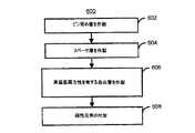
図8は、スピン転移のための低減された書き込み電流密度を有する本発明に基づく磁気素子の一実施形態を提供するための本発明に基づく方法600の一実施形態のフローチャートを示す。方法600について、磁気素子100の文脈で述べる。しかしながら、方法600が、磁気素子100’、100’’、100’’’、200、300、300’、300’’、400、500、500’及び/又は500’’を提供するように構成することを妨げるものではない。ステップ602を介して、固定層110等の固定層を提供する。一実施形態において、ステップ602には、合成固定層を提供する段階が含まれる。スペーサ層120は、ステップ604を介して提供される。ステップ604には、バリア層又は導電層を提供する段階を含み得る。高垂直異方性を有する自由層130が、ステップ606を介して提供される。幾つかの実施形態において、ステップ606に先立って、超高垂直異方性強磁性層又は応力誘起層を提供し得る。ステップ606には、合成自由層を提供する段階を含み得る。そのような実施形態において、ステップ606には、更に、自由層の強磁性層間に高スピン分極層を提供する段階を含み得る。磁気素子200、300、300’、300’’、400、500、500’、及び/又は500’’が提供される場合、追加の固定層、スペーサ層及び幾つかの実施形態では、自由層が、ステップ608を介して提供される。そのような実施形態では、自由層は、高垂直異方性を有し得る。従って、磁気素子100’、100’’、100’’’、100’’’’、200、300、300’、300’’、300’’’、400、500、500’、500’’及び/又は500’’’を提供し得る。 FIG. 8 shows a flowchart of an embodiment of a
より小さいスイッチング電流密度でスピン転移を用いて書き込み得る磁気素子を提供するための方法及びシステムを開示した。本発明について、例示した実施形態に基づき説明したが、当業者は、実施形態に対する変形が存在し得ること、また、これらの変形は、本発明の精神及び範囲内にあることを容易に認識されるであろう。従って、多くの修正が、添付された請求項の精神及び範囲から逸脱することなく当業者によって行い得る。 A method and system have been disclosed for providing a magnetic element that can be written using spin transfer at a lower switching current density. Although the present invention has been described with reference to the illustrated embodiments, those skilled in the art will readily recognize that there may be variations to the embodiments and that these variations are within the spirit and scope of the present invention. It will be. Accordingly, many modifications may be made by one skilled in the art without departing from the spirit and scope of the appended claims.
Claims (13)
Translated fromJapanese非磁性であるスペーサ層と、
第1面外減磁エネルギを有する第1自由層であって、前記第1スペーサ層が前記第1固定層と前記第1自由層との間にある前記第1自由層と、
第2自由層磁化を有し、また、第2面外減磁エネルギを有する第2自由層であって、前記第1自由層及び前記第2自由層が静磁気的に結合されている前記第2自由層と、
非磁性である第2スペーサ層と、
第2固定層であって、前記第2スペーサ層が前記第2自由層と前記第2固定層との間にある前記第2固定層と、が含まれ、
前記磁気素子は、書き込み電流が前記磁気素子を通過する時、前記自由層磁化がスピン転移により切り替えられるように構成され、
前記第1自由層が、前記第1面外減磁エネルギの20パーセント以上且つ100パーセント未満の第1垂直異方性エネルギを有する第1高垂直異方性を有するように構成され、及び/又は、前記第2自由層が、前記第2面外減磁エネルギの20パーセント以上且つ100パーセント未満の第2垂直異方性エネルギを有する第2高垂直異方性を有するように構成される磁気素子。A first fixed layer;
A spacer layer that is non-magnetic;
A first free layer having a first out-of-plane demagnetizing energy, wherein the first spacer layer is between the first fixed layer and the first free layer;
A second free layer having a second free layer magnetization and having a second out-of-plane demagnetizing energy, wherein the first free layer and the second free layer are magnetostatically coupled. Two free layers,
A second spacer layer that is non-magnetic;
A second pinned layer, wherein the second spacer layer is between the second free layer and the second pinned layer, and
The magnetic element is configured such that the free layer magnetization is switched by spin transfer when a write current passes through the magnetic element;
The first free layer is configured to have a first high perpendicular anisotropy having a first perpendicular anisotropy energy of20 percent or more and less than 100 percent of the first out-of-plane demagnetization energy, and / or A magnetic element configured such that the second free layer has a second high perpendicular anisotropy having a second perpendicular anisotropy energy of20% or more and less than 100% of the second out-of-plane demagnetization energy. .
Pt、CoFe、CoFeCr、CoFePt及び/又はCoFeCrPtが含まれる請求項1に記載の磁気素子。For the first free layer and / or the second free layer, Co, CoCr, CoPt, CoCr
The magnetic element according to claim 1, comprising Pt, CoFe, CoFeCr, CoFePt and / or CoFeCrPt.
超高垂直異方性強磁性層と、
高いスピン分極を有する強磁性層と、が含まれ、前記超高垂直異方性強磁性層は、前記第1自由層用の前記超高垂直異方性強磁性層と前記強磁性層との組合せが、前記第1高垂直異方性を有すること、及び/又は、前記第2自由層用の前記超高垂直異方性強磁性層と前記強磁性層の前記組合せが、前記第2高垂直異方性を有すること、を保証するためのものである請求項1に記載の磁気素子。The first free layer and / or the second free layer further includes
An ultra-high perpendicular anisotropic ferromagnetic layer;
A ferromagnetic layer having a high spin polarization, wherein the ultra-high perpendicular anisotropic ferromagnetic layer is a combination of the ultra-high perpendicular anisotropic ferromagnetic layer and the ferromagnetic layer for the first free layer, Having a first high perpendicular anisotropy and / or the combination of the ultra high perpendicular anisotropy ferromagnetic layer and the ferromagnetic layer for the second free layer has the second high perpendicular anisotropy The magnetic element according to claim 1, which guarantees
Applications Claiming Priority (2)
| Application Number | Priority Date | Filing Date | Title |
|---|---|---|---|
| US10/789,334 | 2004-02-26 | ||
| US10/789,334US6992359B2 (en) | 2004-02-26 | 2004-02-26 | Spin transfer magnetic element with free layers having high perpendicular anisotropy and in-plane equilibrium magnetization |
Related Parent Applications (1)
| Application Number | Title | Priority Date | Filing Date |
|---|---|---|---|
| JP2007501017ADivisionJP5281283B2 (en) | 2004-02-26 | 2005-02-24 | Spin transfer magnetic element with free layer with high perpendicular anisotropy and in-plane equilibrium magnetization |
Publications (2)
| Publication Number | Publication Date |
|---|---|
| JP2012119715A JP2012119715A (en) | 2012-06-21 |
| JP5416236B2true JP5416236B2 (en) | 2014-02-12 |
Family
ID=34887255
Family Applications (2)
| Application Number | Title | Priority Date | Filing Date |
|---|---|---|---|
| JP2007501017AExpired - LifetimeJP5281283B2 (en) | 2004-02-26 | 2005-02-24 | Spin transfer magnetic element with free layer with high perpendicular anisotropy and in-plane equilibrium magnetization |
| JP2012022427AExpired - LifetimeJP5416236B2 (en) | 2004-02-26 | 2012-02-03 | Spin transfer magnetic element with free layer with high perpendicular anisotropy and in-plane equilibrium magnetization |
Family Applications Before (1)
| Application Number | Title | Priority Date | Filing Date |
|---|---|---|---|
| JP2007501017AExpired - LifetimeJP5281283B2 (en) | 2004-02-26 | 2005-02-24 | Spin transfer magnetic element with free layer with high perpendicular anisotropy and in-plane equilibrium magnetization |
Country Status (6)
| Country | Link |
|---|---|
| US (4) | US6992359B2 (en) |
| EP (1) | EP1743386B1 (en) |
| JP (2) | JP5281283B2 (en) |
| KR (1) | KR100856185B1 (en) |
| CN (1) | CN1947272A (en) |
| WO (1) | WO2005082061A2 (en) |
Families Citing this family (286)
| Publication number | Priority date | Publication date | Assignee | Title |
|---|---|---|---|---|
| US6980469B2 (en)* | 2003-08-19 | 2005-12-27 | New York University | High speed low power magnetic devices based on current induced spin-momentum transfer |
| US8755222B2 (en) | 2003-08-19 | 2014-06-17 | New York University | Bipolar spin-transfer switching |
| US7911832B2 (en) | 2003-08-19 | 2011-03-22 | New York University | High speed low power magnetic devices based on current induced spin-momentum transfer |
| US7573737B2 (en)* | 2003-08-19 | 2009-08-11 | New York University | High speed low power magnetic devices based on current induced spin-momentum transfer |
| US7282755B2 (en)* | 2003-11-14 | 2007-10-16 | Grandis, Inc. | Stress assisted current driven switching for magnetic memory applications |
| US20110140217A1 (en)* | 2004-02-26 | 2011-06-16 | Grandis, Inc. | Spin transfer magnetic element with free layers having high perpendicular anisotropy and in-plane equilibrium magnetization |
| US6992359B2 (en)* | 2004-02-26 | 2006-01-31 | Grandis, Inc. | Spin transfer magnetic element with free layers having high perpendicular anisotropy and in-plane equilibrium magnetization |
| US7502248B2 (en)* | 2004-05-21 | 2009-03-10 | Samsung Electronics Co., Ltd. | Multi-bit magnetic random access memory device |
| US7611912B2 (en)* | 2004-06-30 | 2009-11-03 | Headway Technologies, Inc. | Underlayer for high performance magnetic tunneling junction MRAM |
| US7576956B2 (en)* | 2004-07-26 | 2009-08-18 | Grandis Inc. | Magnetic tunnel junction having diffusion stop layer |
| US20060128038A1 (en)* | 2004-12-06 | 2006-06-15 | Mahendra Pakala | Method and system for providing a highly textured magnetoresistance element and magnetic memory |
| US7602591B2 (en)* | 2005-06-22 | 2009-10-13 | Tdk Corporation | Exchange-coupled free layer with out-of-plane magnetization |
| US7489541B2 (en)* | 2005-08-23 | 2009-02-10 | Grandis, Inc. | Spin-transfer switching magnetic elements using ferrimagnets and magnetic memories using the magnetic elements |
| US7224601B2 (en) | 2005-08-25 | 2007-05-29 | Grandis Inc. | Oscillating-field assisted spin torque switching of a magnetic tunnel junction memory element |
| US7777261B2 (en) | 2005-09-20 | 2010-08-17 | Grandis Inc. | Magnetic device having stabilized free ferromagnetic layer |
| US7859034B2 (en)* | 2005-09-20 | 2010-12-28 | Grandis Inc. | Magnetic devices having oxide antiferromagnetic layer next to free ferromagnetic layer |
| US7973349B2 (en)* | 2005-09-20 | 2011-07-05 | Grandis Inc. | Magnetic device having multilayered free ferromagnetic layer |
| US20070096229A1 (en)* | 2005-10-28 | 2007-05-03 | Masatoshi Yoshikawa | Magnetoresistive element and magnetic memory device |
| JP2007150265A (en)* | 2005-10-28 | 2007-06-14 | Toshiba Corp | Magnetoresistive element and magnetic storage device |
| US7430135B2 (en)* | 2005-12-23 | 2008-09-30 | Grandis Inc. | Current-switched spin-transfer magnetic devices with reduced spin-transfer switching current density |
| US8535952B2 (en)* | 2006-02-25 | 2013-09-17 | Avalanche Technology, Inc. | Method for manufacturing non-volatile magnetic memory |
| US8183652B2 (en)* | 2007-02-12 | 2012-05-22 | Avalanche Technology, Inc. | Non-volatile magnetic memory with low switching current and high thermal stability |
| US8018011B2 (en)* | 2007-02-12 | 2011-09-13 | Avalanche Technology, Inc. | Low cost multi-state magnetic memory |
| US7732881B2 (en)* | 2006-11-01 | 2010-06-08 | Avalanche Technology, Inc. | Current-confined effect of magnetic nano-current-channel (NCC) for magnetic random access memory (MRAM) |
| US20070253245A1 (en)* | 2006-04-27 | 2007-11-01 | Yadav Technology | High Capacity Low Cost Multi-Stacked Cross-Line Magnetic Memory |
| US20080246104A1 (en)* | 2007-02-12 | 2008-10-09 | Yadav Technology | High Capacity Low Cost Multi-State Magnetic Memory |
| US8363457B2 (en)* | 2006-02-25 | 2013-01-29 | Avalanche Technology, Inc. | Magnetic memory sensing circuit |
| US8058696B2 (en)* | 2006-02-25 | 2011-11-15 | Avalanche Technology, Inc. | High capacity low cost multi-state magnetic memory |
| US8084835B2 (en)* | 2006-10-20 | 2011-12-27 | Avalanche Technology, Inc. | Non-uniform switching based non-volatile magnetic based memory |
| US8508984B2 (en)* | 2006-02-25 | 2013-08-13 | Avalanche Technology, Inc. | Low resistance high-TMR magnetic tunnel junction and process for fabrication thereof |
| US8063459B2 (en)* | 2007-02-12 | 2011-11-22 | Avalanche Technologies, Inc. | Non-volatile magnetic memory element with graded layer |
| US20070246787A1 (en)* | 2006-03-29 | 2007-10-25 | Lien-Chang Wang | On-plug magnetic tunnel junction devices based on spin torque transfer switching |
| US8120949B2 (en)* | 2006-04-27 | 2012-02-21 | Avalanche Technology, Inc. | Low-cost non-volatile flash-RAM memory |
| US7678475B2 (en)* | 2006-05-05 | 2010-03-16 | Slavin Andrei N | Spin-torque devices |
| JP4518049B2 (en)* | 2006-07-03 | 2010-08-04 | ソニー株式会社 | Storage device |
| US7663848B1 (en) | 2006-07-14 | 2010-02-16 | Grandis, Inc. | Magnetic memories utilizing a magnetic element having an engineered free layer |
| US7760474B1 (en)* | 2006-07-14 | 2010-07-20 | Grandis, Inc. | Magnetic element utilizing free layer engineering |
| FR2904724B1 (en)* | 2006-08-03 | 2011-03-04 | Commissariat Energie Atomique | MAGNETIC DEVICE IN THIN LAYERS WITH HIGH PERPENDICULAR SPIN POLARIZATION IN THE LAYER PLAN, MAGNETIC TUNNEL JUNCTION AND SPIN VALVE USING SUCH A DEVICE |
| US7502253B2 (en) | 2006-08-28 | 2009-03-10 | Everspin Technologies, Inc. | Spin-transfer based MRAM with reduced critical current density |
| US7851840B2 (en)* | 2006-09-13 | 2010-12-14 | Grandis Inc. | Devices and circuits based on magnetic tunnel junctions utilizing a multilayer barrier |
| KR100834811B1 (en)* | 2006-11-28 | 2008-06-09 | 고려대학교 산학협력단 | Cobalt-Iron-Silicon-Boron / Platinum Multilayer Thin Film with Vertical Magnetic Anisotropy |
| US7476954B2 (en)* | 2007-01-12 | 2009-01-13 | Headway Technologies, Inc. | TMR device with Hf based seed layer |
| JP4380707B2 (en)* | 2007-01-19 | 2009-12-09 | ソニー株式会社 | Memory element |
| US7869266B2 (en)* | 2007-10-31 | 2011-01-11 | Avalanche Technology, Inc. | Low current switching magnetic tunnel junction design for magnetic memory using domain wall motion |
| US8542524B2 (en)* | 2007-02-12 | 2013-09-24 | Avalanche Technology, Inc. | Magnetic random access memory (MRAM) manufacturing process for a small magnetic tunnel junction (MTJ) design with a low programming current requirement |
| US20090218645A1 (en)* | 2007-02-12 | 2009-09-03 | Yadav Technology Inc. | multi-state spin-torque transfer magnetic random access memory |
| US7692954B2 (en)* | 2007-03-12 | 2010-04-06 | International Business Machines Corporation | Apparatus and method for integrating nonvolatile memory capability within SRAM devices |
| US20080229269A1 (en)* | 2007-03-12 | 2008-09-18 | International Business Machines Corporation | Design structure for integrating nonvolatile memory capability within sram devices |
| JP4682998B2 (en)* | 2007-03-15 | 2011-05-11 | ソニー株式会社 | Memory element and memory |
| US8058697B2 (en)* | 2007-03-26 | 2011-11-15 | Magic Technologies, Inc. | Spin transfer MRAM device with novel magnetic synthetic free layer |
| US7508702B2 (en)* | 2007-04-17 | 2009-03-24 | Macronix International Co., Ltd. | Programming method of magnetic random access memory |
| US8174800B2 (en)* | 2007-05-07 | 2012-05-08 | Canon Anelva Corporation | Magnetoresistive element, method of manufacturing the same, and magnetic multilayered film manufacturing apparatus |
| US7573736B2 (en)* | 2007-05-22 | 2009-08-11 | Taiwan Semiconductor Manufacturing Company | Spin torque transfer MRAM device |
| US7688616B2 (en)* | 2007-06-18 | 2010-03-30 | Taiwan Semicondcutor Manufacturing Company, Ltd. | Device and method of programming a magnetic memory element |
| US7957179B2 (en)* | 2007-06-27 | 2011-06-07 | Grandis Inc. | Magnetic shielding in magnetic multilayer structures |
| US20090027811A1 (en)* | 2007-07-27 | 2009-01-29 | Magic Technologies, Inc. | Spin transfer MRAM device with reduced coefficient of MTJ resistance variation |
| US7982275B2 (en)* | 2007-08-22 | 2011-07-19 | Grandis Inc. | Magnetic element having low saturation magnetization |
| US8497559B2 (en)* | 2007-10-10 | 2013-07-30 | Magic Technologies, Inc. | MRAM with means of controlling magnetic anisotropy |
| US7932571B2 (en)* | 2007-10-11 | 2011-04-26 | Everspin Technologies, Inc. | Magnetic element having reduced current density |
| US8100228B2 (en)* | 2007-10-12 | 2012-01-24 | D B Industries, Inc. | Portable anchorage assembly |
| US20090097303A1 (en)* | 2007-10-15 | 2009-04-16 | Honeywell International Inc. | MRAM with Resistive Property Adjustment |
| US9812184B2 (en) | 2007-10-31 | 2017-11-07 | New York University | Current induced spin-momentum transfer stack with dual insulating layers |
| US7688615B2 (en)* | 2007-12-04 | 2010-03-30 | Macronix International Co., Ltd. | Magnetic random access memory, manufacturing method and programming method thereof |
| US20090168269A1 (en)* | 2007-12-28 | 2009-07-02 | Matthew Joseph Carey | Current perpendicular to plane spin valve with high-polarization material in ap1 layer for reduced spin torque |
| US7929258B2 (en)* | 2008-01-22 | 2011-04-19 | Seagate Technology Llc | Magnetic sensor including a free layer having perpendicular to the plane anisotropy |
| US8802451B2 (en) | 2008-02-29 | 2014-08-12 | Avalanche Technology Inc. | Method for manufacturing high density non-volatile magnetic memory |
| KR100927195B1 (en)* | 2008-04-01 | 2009-11-18 | 이화여자대학교 산학협력단 | Logic and Logic Logic Computing Device Using Dual Magnetic Tunnel Junction Devices Using Spin Torque Conversion |
| US8659852B2 (en) | 2008-04-21 | 2014-02-25 | Seagate Technology Llc | Write-once magentic junction memory array |
| US7999336B2 (en)* | 2008-04-24 | 2011-08-16 | Seagate Technology Llc | ST-RAM magnetic element configurations to reduce switching current |
| US7855911B2 (en)* | 2008-05-23 | 2010-12-21 | Seagate Technology Llc | Reconfigurable magnetic logic device using spin torque |
| US7852663B2 (en)* | 2008-05-23 | 2010-12-14 | Seagate Technology Llc | Nonvolatile programmable logic gates and adders |
| FR2932315B1 (en)* | 2008-06-09 | 2010-06-04 | Commissariat Energie Atomique | MAGNETIC MAGNETIC ELEMENT, PROCESS FOR PRODUCING THE SAME, MAGNETIC FIELD SENSOR, MAGNETIC MEMORY AND MAGNETIC LOGIC DOOR USING THE SAME |
| WO2009157101A1 (en)* | 2008-06-25 | 2009-12-30 | 富士電機ホールディングス株式会社 | Magnetic memory element and its driving method and nonvolatile memory device |
| US7804709B2 (en)* | 2008-07-18 | 2010-09-28 | Seagate Technology Llc | Diode assisted switching spin-transfer torque memory unit |
| US8223532B2 (en) | 2008-08-07 | 2012-07-17 | Seagate Technology Llc | Magnetic field assisted STRAM cells |
| US7935435B2 (en)* | 2008-08-08 | 2011-05-03 | Seagate Technology Llc | Magnetic memory cell construction |
| US8134864B2 (en)* | 2008-08-14 | 2012-03-13 | Regents Of The University Of Minnesota | Exchange-assisted spin transfer torque switching |
| US7881098B2 (en)* | 2008-08-26 | 2011-02-01 | Seagate Technology Llc | Memory with separate read and write paths |
| EP2333826B1 (en)* | 2008-09-03 | 2014-09-03 | Fuji Electric Co., Ltd. | Magnetic memory element and storage device using same |
| US7894248B2 (en)* | 2008-09-12 | 2011-02-22 | Grandis Inc. | Programmable and redundant circuitry based on magnetic tunnel junction (MTJ) |
| US20100075599A1 (en)* | 2008-09-22 | 2010-03-25 | Haiwen Xi | Data Transmission and Exchange Using Spin Waves |
| US8482966B2 (en)* | 2008-09-24 | 2013-07-09 | Qualcomm Incorporated | Magnetic element utilizing protective sidewall passivation |
| US9929211B2 (en)* | 2008-09-24 | 2018-03-27 | Qualcomm Incorporated | Reducing spin pumping induced damping of a free layer of a memory device |
| US7985994B2 (en) | 2008-09-29 | 2011-07-26 | Seagate Technology Llc | Flux-closed STRAM with electronically reflective insulative spacer |
| US7826256B2 (en) | 2008-09-29 | 2010-11-02 | Seagate Technology Llc | STRAM with compensation element |
| US7940551B2 (en) | 2008-09-29 | 2011-05-10 | Seagate Technology, Llc | STRAM with electronically reflective insulative spacer |
| US8310861B2 (en)* | 2008-09-30 | 2012-11-13 | Micron Technology, Inc. | STT-MRAM cell structure incorporating piezoelectric stress material |
| US7876603B2 (en) | 2008-09-30 | 2011-01-25 | Micron Technology, Inc. | Spin current generator for STT-MRAM or other spintronics applications |
| US8102700B2 (en) | 2008-09-30 | 2012-01-24 | Micron Technology, Inc. | Unidirectional spin torque transfer magnetic memory cell structure |
| US7746687B2 (en) | 2008-09-30 | 2010-06-29 | Seagate Technology, Llc | Thermally assisted multi-bit MRAM |
| US8487390B2 (en)* | 2008-10-08 | 2013-07-16 | Seagate Technology Llc | Memory cell with stress-induced anisotropy |
| US8169810B2 (en) | 2008-10-08 | 2012-05-01 | Seagate Technology Llc | Magnetic memory with asymmetric energy barrier |
| US8089132B2 (en)* | 2008-10-09 | 2012-01-03 | Seagate Technology Llc | Magnetic memory with phonon glass electron crystal material |
| US7880209B2 (en)* | 2008-10-09 | 2011-02-01 | Seagate Technology Llc | MRAM cells including coupled free ferromagnetic layers for stabilization |
| US8039913B2 (en)* | 2008-10-09 | 2011-10-18 | Seagate Technology Llc | Magnetic stack with laminated layer |
| US20100091564A1 (en)* | 2008-10-10 | 2010-04-15 | Seagate Technology Llc | Magnetic stack having reduced switching current |
| US8217478B2 (en) | 2008-10-10 | 2012-07-10 | Seagate Technology Llc | Magnetic stack with oxide to reduce switching current |
| US20100102405A1 (en)* | 2008-10-27 | 2010-04-29 | Seagate Technology Llc | St-ram employing a spin filter |
| US9165625B2 (en)* | 2008-10-30 | 2015-10-20 | Seagate Technology Llc | ST-RAM cells with perpendicular anisotropy |
| US8045366B2 (en) | 2008-11-05 | 2011-10-25 | Seagate Technology Llc | STRAM with composite free magnetic element |
| US7944738B2 (en) | 2008-11-05 | 2011-05-17 | Micron Technology, Inc. | Spin torque transfer cell structure utilizing field-induced antiferromagnetic or ferromagnetic coupling |
| US8043732B2 (en) | 2008-11-11 | 2011-10-25 | Seagate Technology Llc | Memory cell with radial barrier |
| US7826181B2 (en)* | 2008-11-12 | 2010-11-02 | Seagate Technology Llc | Magnetic memory with porous non-conductive current confinement layer |
| US8289756B2 (en)* | 2008-11-25 | 2012-10-16 | Seagate Technology Llc | Non volatile memory including stabilizing structures |
| US7940600B2 (en)* | 2008-12-02 | 2011-05-10 | Seagate Technology Llc | Non-volatile memory with stray magnetic field compensation |
| US7859892B2 (en) | 2008-12-03 | 2010-12-28 | Seagate Technology Llc | Magnetic random access memory with dual spin torque reference layers |
| US8553449B2 (en) | 2009-01-09 | 2013-10-08 | Micron Technology, Inc. | STT-MRAM cell structures |
| US7957182B2 (en)* | 2009-01-12 | 2011-06-07 | Micron Technology, Inc. | Memory cell having nonmagnetic filament contact and methods of operating and fabricating the same |
| JP4952725B2 (en) | 2009-01-14 | 2012-06-13 | ソニー株式会社 | Nonvolatile magnetic memory device |
| JP5582037B2 (en)* | 2009-01-27 | 2014-09-03 | 日本電気株式会社 | Nonvolatile logic circuit |
| US7826259B2 (en)* | 2009-01-29 | 2010-11-02 | Seagate Technology Llc | Staggered STRAM cell |
| US7936592B2 (en)* | 2009-02-03 | 2011-05-03 | Seagate Technology Llc | Non-volatile memory cell with precessional switching |
| US8053255B2 (en)* | 2009-03-03 | 2011-11-08 | Seagate Technology Llc | STRAM with compensation element and method of making the same |
| TWI443656B (en)* | 2009-04-16 | 2014-07-01 | Univ Nat Yunlin Sci & Tech | Magnetic-stack structure and manufacturing method thereof |
| US7936598B2 (en) | 2009-04-28 | 2011-05-03 | Seagate Technology | Magnetic stack having assist layer |
| EP2249349B1 (en)* | 2009-05-08 | 2012-02-08 | Crocus Technology | Magnetic memory with a thermally assisted writing procedure and reduced writng field |
| EP2249350B1 (en)* | 2009-05-08 | 2012-02-01 | Crocus Technology | Magnetic memory with a thermally assisted spin transfer torque writing procedure using a low writing current |
| KR101687845B1 (en) | 2009-05-19 | 2016-12-19 | 아이아이아이 홀딩스 3, 엘엘씨 | Magnetic memory element and storage device using same |
| US8183653B2 (en)* | 2009-07-13 | 2012-05-22 | Seagate Technology Llc | Magnetic tunnel junction having coherent tunneling structure |
| US7999338B2 (en) | 2009-07-13 | 2011-08-16 | Seagate Technology Llc | Magnetic stack having reference layers with orthogonal magnetization orientation directions |
| US8125746B2 (en)* | 2009-07-13 | 2012-02-28 | Seagate Technology Llc | Magnetic sensor with perpendicular anisotrophy free layer and side shields |
| US10446209B2 (en) | 2009-08-10 | 2019-10-15 | Samsung Semiconductor Inc. | Method and system for providing magnetic tunneling junction elements having improved performance through capping layer induced perpendicular anisotropy and memories using such magnetic elements |
| US8779538B2 (en)* | 2009-08-10 | 2014-07-15 | Samsung Electronics Co., Ltd. | Magnetic tunneling junction seed, capping, and spacer layer materials |
| US8913350B2 (en)* | 2009-08-10 | 2014-12-16 | Grandis, Inc. | Method and system for providing magnetic tunneling junction elements having improved performance through capping layer induced perpendicular anisotropy and memories using such magnetic elements |
| US20110031569A1 (en)* | 2009-08-10 | 2011-02-10 | Grandis, Inc. | Method and system for providing magnetic tunneling junction elements having improved performance through capping layer induced perpendicular anisotropy and memories using such magnetic elements |
| US8445979B2 (en) | 2009-09-11 | 2013-05-21 | Samsung Electronics Co., Ltd. | Magnetic memory devices including magnetic layers separated by tunnel barriers |
| US8558331B2 (en)* | 2009-12-08 | 2013-10-15 | Qualcomm Incorporated | Magnetic tunnel junction device |
| KR101658394B1 (en)* | 2009-12-15 | 2016-09-22 | 삼성전자 주식회사 | Magnetic Tunnel Junction device, method of manufacturing the same and electronic device comprising the same |
| KR101676824B1 (en) | 2010-06-15 | 2016-11-18 | 삼성전자주식회사 | Magnetic memory device |
| WO2012004883A1 (en)* | 2010-07-09 | 2012-01-12 | 国立大学法人東北大学 | Magnetoresistive effect element and random access memory using same |
| US8546896B2 (en)* | 2010-07-16 | 2013-10-01 | Grandis, Inc. | Magnetic tunneling junction elements having magnetic substructures(s) with a perpendicular anisotropy and memories using such magnetic elements |
| US8374048B2 (en)* | 2010-08-11 | 2013-02-12 | Grandis, Inc. | Method and system for providing magnetic tunneling junction elements having a biaxial anisotropy |
| US8399941B2 (en) | 2010-11-05 | 2013-03-19 | Grandis, Inc. | Magnetic junction elements having an easy cone anisotropy and a magnetic memory using such magnetic junction elements |
| KR101463948B1 (en) | 2010-11-08 | 2014-11-27 | 삼성전자주식회사 | Magnetic memory devices |
| US8405171B2 (en) | 2010-11-16 | 2013-03-26 | Seagate Technology Llc | Memory cell with phonon-blocking insulating layer |
| US8508973B2 (en) | 2010-11-16 | 2013-08-13 | Seagate Technology Llc | Method of switching out-of-plane magnetic tunnel junction cells |
| US8274811B2 (en) | 2010-11-22 | 2012-09-25 | Headway Technologies, Inc. | Assisting FGL oscillations with perpendicular anisotropy for MAMR |
| JP5794892B2 (en)* | 2010-11-26 | 2015-10-14 | ルネサスエレクトロニクス株式会社 | Magnetic memory |
| CN102569642B (en) | 2010-12-07 | 2016-08-03 | 三星电子株式会社 | Memory node, the magnetic memory device including this memory node and manufacture method thereof |
| US8704319B2 (en)* | 2010-12-31 | 2014-04-22 | Samsung Electronics Co., Ltd. | Method and system for providing magnetic layers having insertion layers for use in spin transfer torque memories |
| US9478730B2 (en) | 2010-12-31 | 2016-10-25 | Samsung Electronics Co., Ltd. | Method and system for providing magnetic layers having insertion layers for use in spin transfer torque memories |
| US8432009B2 (en)* | 2010-12-31 | 2013-04-30 | Grandis, Inc. | Method and system for providing magnetic layers having insertion layers for use in spin transfer torque memories |
| CN102280574B (en) | 2011-01-07 | 2014-04-16 | 江苏多维科技有限公司 | Thin film magnetoresistance sensing element, combination of multiple sensing elements, and electronic device coupled with combination |
| JP5691604B2 (en)* | 2011-02-17 | 2015-04-01 | 富士通株式会社 | Magnetic tunnel junction device and magnetic random access memory |
| JP5732894B2 (en)* | 2011-02-17 | 2015-06-10 | 富士通株式会社 | Magnetic tunnel junction device and magnetic random access memory |
| US8947914B2 (en) | 2011-03-18 | 2015-02-03 | Samsung Electronics Co., Ltd. | Magnetic tunneling junction devices, memories, electronic systems, and memory systems, and methods of fabricating the same |
| KR101368298B1 (en)* | 2011-04-06 | 2014-03-03 | 고려대학교 산학협력단 | a device for generating high frequency microwave and high frequency magnetic field using spin transfer torque |
| US8541855B2 (en)* | 2011-05-10 | 2013-09-24 | Magic Technologies, Inc. | Co/Ni multilayers with improved out-of-plane anisotropy for magnetic device applications |
| FR2976396B1 (en)* | 2011-06-07 | 2013-07-12 | Commissariat Energie Atomique | MAGNETIC STACK AND MEMORY POINT COMPRISING SUCH A STACK |
| US8553451B2 (en) | 2011-06-24 | 2013-10-08 | Micron Technology, Inc. | Spin-torque transfer memory cell structures with symmetric switching and single direction programming |
| US8766383B2 (en) | 2011-07-07 | 2014-07-01 | Samsung Electronics Co., Ltd. | Method and system for providing a magnetic junction using half metallic ferromagnets |
| JP5814680B2 (en)* | 2011-07-29 | 2015-11-17 | 株式会社東芝 | Magnetoresistive element and magnetic memory |
| WO2013020569A1 (en)* | 2011-08-10 | 2013-02-14 | Christian-Albrechts-Universität Zu Kiel | Magnetoresistive memory with low critical current for magnetization switching |
| KR101912223B1 (en) | 2011-08-16 | 2019-01-04 | 삼성전자주식회사 | Stacked mram device and memory system having the same |
| US8704320B2 (en)* | 2011-09-12 | 2014-04-22 | Qualcomm Incorporated | Strain induced reduction of switching current in spin-transfer torque switching devices |
| US9036308B2 (en)* | 2011-09-21 | 2015-05-19 | Seagate Technology Llc | Varyinig morphology in magnetic sensor sub-layers |
| US9245608B2 (en) | 2011-09-22 | 2016-01-26 | Qualcomm Incorporated | Thermally tolerant perpendicular magnetic anisotropy coupled elements for spin-transfer torque switching device |
| US8860159B2 (en) | 2011-10-20 | 2014-10-14 | The United States Of America As Represented By The Secretary Of The Army | Spintronic electronic device and circuits |
| US8829901B2 (en)* | 2011-11-04 | 2014-09-09 | Honeywell International Inc. | Method of using a magnetoresistive sensor in second harmonic detection mode for sensing weak magnetic fields |
| JP5987302B2 (en)* | 2011-11-30 | 2016-09-07 | ソニー株式会社 | Memory element and memory device |
| KR102043362B1 (en)* | 2011-12-20 | 2019-11-12 | 삼성전자주식회사 | Method and system for providing magnetic layers having insertion layers for use in spin transfer torque memories |
| US8698259B2 (en) | 2011-12-20 | 2014-04-15 | Samsung Electronics Co., Ltd. | Method and system for providing a magnetic tunneling junction using thermally assisted switching |
| US8710602B2 (en)* | 2011-12-20 | 2014-04-29 | Samsung Electronics Co., Ltd. | Method and system for providing magnetic junctions having improved characteristics |
| US9007818B2 (en) | 2012-03-22 | 2015-04-14 | Micron Technology, Inc. | Memory cells, semiconductor device structures, systems including such cells, and methods of fabrication |
| KR102130054B1 (en)* | 2012-06-07 | 2020-07-06 | 삼성전자주식회사 | MAGNETIC TUNNELING JUNCTION SEED, CAPPING, and SPACER LAYER MATERIALS |
| US8923038B2 (en)* | 2012-06-19 | 2014-12-30 | Micron Technology, Inc. | Memory cells, semiconductor device structures, memory systems, and methods of fabrication |
| US9054030B2 (en) | 2012-06-19 | 2015-06-09 | Micron Technology, Inc. | Memory cells, semiconductor device structures, memory systems, and methods of fabrication |
| US8773821B2 (en)* | 2012-10-05 | 2014-07-08 | Nve Corporation | Magnetoresistive-based mixed anisotropy high field sensor |
| US9082950B2 (en) | 2012-10-17 | 2015-07-14 | New York University | Increased magnetoresistance in an inverted orthogonal spin transfer layer stack |
| US9082888B2 (en) | 2012-10-17 | 2015-07-14 | New York University | Inverted orthogonal spin transfer layer stack |
| JP6342113B2 (en)* | 2012-12-19 | 2018-06-13 | サムスン エレクトロニクス カンパニー リミテッド | Method and system for providing a magnetic junction with improved characteristics |
| US8786039B2 (en)* | 2012-12-20 | 2014-07-22 | Samsung Electronics Co., Ltd. | Method and system for providing magnetic junctions having engineered perpendicular magnetic anisotropy |
| KR102199622B1 (en)* | 2013-01-11 | 2021-01-08 | 삼성전자주식회사 | Method and system for providing magnetic tunneling juntion elements having easy cone anisotropy |
| US9379315B2 (en) | 2013-03-12 | 2016-06-28 | Micron Technology, Inc. | Memory cells, methods of fabrication, semiconductor device structures, and memory systems |
| US8982613B2 (en) | 2013-06-17 | 2015-03-17 | New York University | Scalable orthogonal spin transfer magnetic random access memory devices with reduced write error rates |
| JP6122353B2 (en) | 2013-06-25 | 2017-04-26 | ルネサスエレクトロニクス株式会社 | Semiconductor package |
| US9368714B2 (en) | 2013-07-01 | 2016-06-14 | Micron Technology, Inc. | Memory cells, methods of operation and fabrication, semiconductor device structures, and memory systems |
| US9466787B2 (en) | 2013-07-23 | 2016-10-11 | Micron Technology, Inc. | Memory cells, methods of fabrication, semiconductor device structures, memory systems, and electronic systems |
| US9461242B2 (en) | 2013-09-13 | 2016-10-04 | Micron Technology, Inc. | Magnetic memory cells, methods of fabrication, semiconductor devices, memory systems, and electronic systems |
| US9608197B2 (en) | 2013-09-18 | 2017-03-28 | Micron Technology, Inc. | Memory cells, methods of fabrication, and semiconductor devices |
| US9349391B2 (en) | 2013-12-04 | 2016-05-24 | HGST Netherlands B.V. | Controlling magnetic layer anisotropy field by oblique angle static deposition |
| US9529060B2 (en)* | 2014-01-09 | 2016-12-27 | Allegro Microsystems, Llc | Magnetoresistance element with improved response to magnetic fields |
| US10454024B2 (en) | 2014-02-28 | 2019-10-22 | Micron Technology, Inc. | Memory cells, methods of fabrication, and memory devices |
| US9344345B2 (en)* | 2014-03-19 | 2016-05-17 | Micron Technology, Inc. | Memory cells having a self-aligning polarizer |
| US9281466B2 (en) | 2014-04-09 | 2016-03-08 | Micron Technology, Inc. | Memory cells, semiconductor structures, semiconductor devices, and methods of fabrication |
| US9269888B2 (en) | 2014-04-18 | 2016-02-23 | Micron Technology, Inc. | Memory cells, methods of fabrication, and semiconductor devices |
| US9336797B2 (en) | 2014-05-29 | 2016-05-10 | HGST Netherlands B.V. | Extended spin torque oscillator |
| US9324939B2 (en) | 2014-07-01 | 2016-04-26 | Qualcomm Incorporated | Synthetic antiferromagnet (SAF) coupled free layer for perpendicular magnetic tunnel junction (p-MTJ) |
| US9263667B1 (en) | 2014-07-25 | 2016-02-16 | Spin Transfer Technologies, Inc. | Method for manufacturing MTJ memory device |
| US9337412B2 (en) | 2014-09-22 | 2016-05-10 | Spin Transfer Technologies, Inc. | Magnetic tunnel junction structure for MRAM device |
| US9349945B2 (en) | 2014-10-16 | 2016-05-24 | Micron Technology, Inc. | Memory cells, semiconductor devices, and methods of fabrication |
| US9768377B2 (en) | 2014-12-02 | 2017-09-19 | Micron Technology, Inc. | Magnetic cell structures, and methods of fabrication |
| US10439131B2 (en) | 2015-01-15 | 2019-10-08 | Micron Technology, Inc. | Methods of forming semiconductor devices including tunnel barrier materials |
| US9758359B2 (en) | 2015-03-25 | 2017-09-12 | K-Line Industries, Inc. | Jack system |
| US10468590B2 (en) | 2015-04-21 | 2019-11-05 | Spin Memory, Inc. | High annealing temperature perpendicular magnetic anisotropy structure for magnetic random access memory |
| US9728712B2 (en) | 2015-04-21 | 2017-08-08 | Spin Transfer Technologies, Inc. | Spin transfer torque structure for MRAM devices having a spin current injection capping layer |
| US9853206B2 (en) | 2015-06-16 | 2017-12-26 | Spin Transfer Technologies, Inc. | Precessional spin current structure for MRAM |
| US9773974B2 (en) | 2015-07-30 | 2017-09-26 | Spin Transfer Technologies, Inc. | Polishing stop layer(s) for processing arrays of semiconductor elements |
| US10163479B2 (en) | 2015-08-14 | 2018-12-25 | Spin Transfer Technologies, Inc. | Method and apparatus for bipolar memory write-verify |
| KR102482372B1 (en)* | 2015-10-15 | 2022-12-29 | 삼성전자주식회사 | Magnetoresistive random access device and method of manufacturing the same |
| CN105355780B (en)* | 2015-11-03 | 2018-12-25 | 湖北中部慧易数据科技有限公司 | A kind of magnetic element, storage system and its write operation method |
| US9741926B1 (en) | 2016-01-28 | 2017-08-22 | Spin Transfer Technologies, Inc. | Memory cell having magnetic tunnel junction and thermal stability enhancement layer |
| US10446210B2 (en) | 2016-09-27 | 2019-10-15 | Spin Memory, Inc. | Memory instruction pipeline with a pre-read stage for a write operation for reducing power consumption in a memory device that uses dynamic redundancy registers |
| US11151042B2 (en) | 2016-09-27 | 2021-10-19 | Integrated Silicon Solution, (Cayman) Inc. | Error cache segmentation for power reduction |
| US10991410B2 (en) | 2016-09-27 | 2021-04-27 | Spin Memory, Inc. | Bi-polar write scheme |
| US10460781B2 (en) | 2016-09-27 | 2019-10-29 | Spin Memory, Inc. | Memory device with a dual Y-multiplexer structure for performing two simultaneous operations on the same row of a memory bank |
| US11119936B2 (en) | 2016-09-27 | 2021-09-14 | Spin Memory, Inc. | Error cache system with coarse and fine segments for power optimization |
| US11119910B2 (en) | 2016-09-27 | 2021-09-14 | Spin Memory, Inc. | Heuristics for selecting subsegments for entry in and entry out operations in an error cache system with coarse and fine grain segments |
| US10366774B2 (en) | 2016-09-27 | 2019-07-30 | Spin Memory, Inc. | Device with dynamic redundancy registers |
| US10437491B2 (en) | 2016-09-27 | 2019-10-08 | Spin Memory, Inc. | Method of processing incomplete memory operations in a memory device during a power up sequence and a power down sequence using a dynamic redundancy register |
| US10437723B2 (en) | 2016-09-27 | 2019-10-08 | Spin Memory, Inc. | Method of flushing the contents of a dynamic redundancy register to a secure storage area during a power down in a memory device |
| US10818331B2 (en) | 2016-09-27 | 2020-10-27 | Spin Memory, Inc. | Multi-chip module for MRAM devices with levels of dynamic redundancy registers |
| US10546625B2 (en) | 2016-09-27 | 2020-01-28 | Spin Memory, Inc. | Method of optimizing write voltage based on error buffer occupancy |
| US10360964B2 (en) | 2016-09-27 | 2019-07-23 | Spin Memory, Inc. | Method of writing contents in memory during a power up sequence using a dynamic redundancy register in a memory device |
| US10628316B2 (en) | 2016-09-27 | 2020-04-21 | Spin Memory, Inc. | Memory device with a plurality of memory banks where each memory bank is associated with a corresponding memory instruction pipeline and a dynamic redundancy register |
| US10665777B2 (en) | 2017-02-28 | 2020-05-26 | Spin Memory, Inc. | Precessional spin current structure with non-magnetic insertion layer for MRAM |
| US10672976B2 (en) | 2017-02-28 | 2020-06-02 | Spin Memory, Inc. | Precessional spin current structure with high in-plane magnetization for MRAM |
| US10332576B2 (en)* | 2017-06-07 | 2019-06-25 | International Business Machines Corporation | Magnetic exchange coupled MTJ free layer with double tunnel barriers having low switching current and high data retention |
| US10510390B2 (en)* | 2017-06-07 | 2019-12-17 | International Business Machines Corporation | Magnetic exchange coupled MTJ free layer having low switching current and high data retention |
| US10032978B1 (en) | 2017-06-27 | 2018-07-24 | Spin Transfer Technologies, Inc. | MRAM with reduced stray magnetic fields |
| KR101856906B1 (en)* | 2017-08-31 | 2018-05-10 | 연세대학교 산학협력단 | Spin-Orbit Torque Magnetic Device |
| US10481976B2 (en) | 2017-10-24 | 2019-11-19 | Spin Memory, Inc. | Forcing bits as bad to widen the window between the distributions of acceptable high and low resistive bits thereby lowering the margin and increasing the speed of the sense amplifiers |
| US10529439B2 (en) | 2017-10-24 | 2020-01-07 | Spin Memory, Inc. | On-the-fly bit failure detection and bit redundancy remapping techniques to correct for fixed bit defects |
| US10489245B2 (en) | 2017-10-24 | 2019-11-26 | Spin Memory, Inc. | Forcing stuck bits, waterfall bits, shunt bits and low TMR bits to short during testing and using on-the-fly bit failure detection and bit redundancy remapping techniques to correct them |
| US10656994B2 (en) | 2017-10-24 | 2020-05-19 | Spin Memory, Inc. | Over-voltage write operation of tunnel magnet-resistance (“TMR”) memory device and correcting failure bits therefrom by using on-the-fly bit failure detection and bit redundancy remapping techniques |
| US10679685B2 (en) | 2017-12-27 | 2020-06-09 | Spin Memory, Inc. | Shared bit line array architecture for magnetoresistive memory |
| US10360962B1 (en) | 2017-12-28 | 2019-07-23 | Spin Memory, Inc. | Memory array with individually trimmable sense amplifiers |
| US10891997B2 (en) | 2017-12-28 | 2021-01-12 | Spin Memory, Inc. | Memory array with horizontal source line and a virtual source line |
| US10395712B2 (en) | 2017-12-28 | 2019-08-27 | Spin Memory, Inc. | Memory array with horizontal source line and sacrificial bitline per virtual source |
| US10516094B2 (en) | 2017-12-28 | 2019-12-24 | Spin Memory, Inc. | Process for creating dense pillars using multiple exposures for MRAM fabrication |
| US10811594B2 (en) | 2017-12-28 | 2020-10-20 | Spin Memory, Inc. | Process for hard mask development for MRAM pillar formation using photolithography |
| US10395711B2 (en) | 2017-12-28 | 2019-08-27 | Spin Memory, Inc. | Perpendicular source and bit lines for an MRAM array |
| US10424726B2 (en) | 2017-12-28 | 2019-09-24 | Spin Memory, Inc. | Process for improving photoresist pillar adhesion during MRAM fabrication |
| US10840436B2 (en) | 2017-12-29 | 2020-11-17 | Spin Memory, Inc. | Perpendicular magnetic anisotropy interface tunnel junction devices and methods of manufacture |
| US10236047B1 (en) | 2017-12-29 | 2019-03-19 | Spin Memory, Inc. | Shared oscillator (STNO) for MRAM array write-assist in orthogonal STT-MRAM |
| US10360961B1 (en) | 2017-12-29 | 2019-07-23 | Spin Memory, Inc. | AC current pre-charge write-assist in orthogonal STT-MRAM |
| US10367139B2 (en) | 2017-12-29 | 2019-07-30 | Spin Memory, Inc. | Methods of manufacturing magnetic tunnel junction devices |
| US10199083B1 (en) | 2017-12-29 | 2019-02-05 | Spin Transfer Technologies, Inc. | Three-terminal MRAM with ac write-assist for low read disturb |
| US10270027B1 (en) | 2017-12-29 | 2019-04-23 | Spin Memory, Inc. | Self-generating AC current assist in orthogonal STT-MRAM |
| US10424723B2 (en) | 2017-12-29 | 2019-09-24 | Spin Memory, Inc. | Magnetic tunnel junction devices including an optimization layer |
| US10546624B2 (en) | 2017-12-29 | 2020-01-28 | Spin Memory, Inc. | Multi-port random access memory |
| US10784439B2 (en) | 2017-12-29 | 2020-09-22 | Spin Memory, Inc. | Precessional spin current magnetic tunnel junction devices and methods of manufacture |
| US10236048B1 (en) | 2017-12-29 | 2019-03-19 | Spin Memory, Inc. | AC current write-assist in orthogonal STT-MRAM |
| US10886330B2 (en) | 2017-12-29 | 2021-01-05 | Spin Memory, Inc. | Memory device having overlapping magnetic tunnel junctions in compliance with a reference pitch |
| US10840439B2 (en) | 2017-12-29 | 2020-11-17 | Spin Memory, Inc. | Magnetic tunnel junction (MTJ) fabrication methods and systems |
| US10229724B1 (en) | 2017-12-30 | 2019-03-12 | Spin Memory, Inc. | Microwave write-assist in series-interconnected orthogonal STT-MRAM devices |
| US10339993B1 (en) | 2017-12-30 | 2019-07-02 | Spin Memory, Inc. | Perpendicular magnetic tunnel junction device with skyrmionic assist layers for free layer switching |
| US10141499B1 (en) | 2017-12-30 | 2018-11-27 | Spin Transfer Technologies, Inc. | Perpendicular magnetic tunnel junction device with offset precessional spin current layer |
| US10319900B1 (en) | 2017-12-30 | 2019-06-11 | Spin Memory, Inc. | Perpendicular magnetic tunnel junction device with precessional spin current layer having a modulated moment density |
| US10255962B1 (en) | 2017-12-30 | 2019-04-09 | Spin Memory, Inc. | Microwave write-assist in orthogonal STT-MRAM |
| US10236439B1 (en) | 2017-12-30 | 2019-03-19 | Spin Memory, Inc. | Switching and stability control for perpendicular magnetic tunnel junction device |
| US10468588B2 (en) | 2018-01-05 | 2019-11-05 | Spin Memory, Inc. | Perpendicular magnetic tunnel junction device with skyrmionic enhancement layers for the precessional spin current magnetic layer |
| US10438996B2 (en) | 2018-01-08 | 2019-10-08 | Spin Memory, Inc. | Methods of fabricating magnetic tunnel junctions integrated with selectors |
| US10438995B2 (en) | 2018-01-08 | 2019-10-08 | Spin Memory, Inc. | Devices including magnetic tunnel junctions integrated with selectors |
| US10411069B1 (en) | 2018-02-17 | 2019-09-10 | GlobalFoundries, Inc. | Integrated circuits including magnetic random access memory structures and methods for fabricating the same |
| US10468456B2 (en)* | 2018-02-17 | 2019-11-05 | Globalfoundries Inc. | Integrated circuits including magnetic random access memory structures having reduced switching energy barriers for differential bit operation and methods for fabricating the same |
| US10381406B1 (en)* | 2018-02-17 | 2019-08-13 | GlobalFoundries, Inc. | Integrated circuits including magnetic random access memory structures having reduced switching energy barriers for dual bit operation and methods for fabricating the same |
| US11424404B2 (en) | 2018-02-27 | 2022-08-23 | Tdk Corporation | Ferromagnetic laminated film, spin current magnetization rotating element, magnetoresistance effect element, and magnetic memory |
| US10388861B1 (en) | 2018-03-08 | 2019-08-20 | Spin Memory, Inc. | Magnetic tunnel junction wafer adaptor used in magnetic annealing furnace and method of using the same |
| US10446744B2 (en) | 2018-03-08 | 2019-10-15 | Spin Memory, Inc. | Magnetic tunnel junction wafer adaptor used in magnetic annealing furnace and method of using the same |
| US11107978B2 (en) | 2018-03-23 | 2021-08-31 | Spin Memory, Inc. | Methods of manufacturing three-dimensional arrays with MTJ devices including a free magnetic trench layer and a planar reference magnetic layer |
| US20190296220A1 (en) | 2018-03-23 | 2019-09-26 | Spin Transfer Technologies, Inc. | Magnetic Tunnel Junction Devices Including an Annular Free Magnetic Layer and a Planar Reference Magnetic Layer |
| US11107974B2 (en) | 2018-03-23 | 2021-08-31 | Spin Memory, Inc. | Magnetic tunnel junction devices including a free magnetic trench layer and a planar reference magnetic layer |
| US10784437B2 (en) | 2018-03-23 | 2020-09-22 | Spin Memory, Inc. | Three-dimensional arrays with MTJ devices including a free magnetic trench layer and a planar reference magnetic layer |
| US10943951B2 (en) | 2018-04-03 | 2021-03-09 | National University Of Singapore | Spin orbit torque magnetic random access memory structures and methods for fabrication |
| US10411185B1 (en) | 2018-05-30 | 2019-09-10 | Spin Memory, Inc. | Process for creating a high density magnetic tunnel junction array test platform |
| CN108732791B (en)* | 2018-06-01 | 2020-05-12 | 厦门大学 | A variable wavelength two-dimensional optical rotation device with controllable polarizability and its preparation method |
| US10559338B2 (en) | 2018-07-06 | 2020-02-11 | Spin Memory, Inc. | Multi-bit cell read-out techniques |
| US10692569B2 (en) | 2018-07-06 | 2020-06-23 | Spin Memory, Inc. | Read-out techniques for multi-bit cells |
| US10600478B2 (en) | 2018-07-06 | 2020-03-24 | Spin Memory, Inc. | Multi-bit cell read-out techniques for MRAM cells with mixed pinned magnetization orientations |
| US10593396B2 (en) | 2018-07-06 | 2020-03-17 | Spin Memory, Inc. | Multi-bit cell read-out techniques for MRAM cells with mixed pinned magnetization orientations |
| US10650875B2 (en) | 2018-08-21 | 2020-05-12 | Spin Memory, Inc. | System for a wide temperature range nonvolatile memory |
| US10699761B2 (en) | 2018-09-18 | 2020-06-30 | Spin Memory, Inc. | Word line decoder memory architecture |
| US10971680B2 (en) | 2018-10-01 | 2021-04-06 | Spin Memory, Inc. | Multi terminal device stack formation methods |
| US11621293B2 (en) | 2018-10-01 | 2023-04-04 | Integrated Silicon Solution, (Cayman) Inc. | Multi terminal device stack systems and methods |
| US10580827B1 (en) | 2018-11-16 | 2020-03-03 | Spin Memory, Inc. | Adjustable stabilizer/polarizer method for MRAM with enhanced stability and efficient switching |
| KR102316542B1 (en) | 2018-11-22 | 2021-10-22 | 한양대학교 산학협력단 | Memory device |
| WO2020117341A1 (en)* | 2018-12-06 | 2020-06-11 | Sandisk Technologies Llc | Spin-transfer torque mram with assist layers and methods of operating the same |
| US10726892B2 (en)* | 2018-12-06 | 2020-07-28 | Sandisk Technologies Llc | Metallic magnetic memory devices for cryogenic operation and methods of operating the same |
| US11107979B2 (en) | 2018-12-28 | 2021-08-31 | Spin Memory, Inc. | Patterned silicide structures and methods of manufacture |
| US11094359B2 (en)* | 2019-01-24 | 2021-08-17 | Spin Memory, Inc. | High retention multi-level-series magnetic random-access memory |
| US11968842B2 (en)* | 2020-08-11 | 2024-04-23 | National University Of Singapore | Spin-orbit torque device, method for fabricating a spin-orbit torque device and method for switching a switchable magnetization of a spin-orbit torque device |
| US12382839B2 (en)* | 2022-01-07 | 2025-08-05 | Samsung Electronics Co., Ltd. | Magnetic tunneling junction device and memory device including the same |
| US12359904B2 (en) | 2023-01-26 | 2025-07-15 | Allegro Microsystems, Llc | Method of manufacturing angle sensors including magnetoresistance elements including different types of antiferromagnetic materials |
| US12352832B2 (en) | 2023-01-30 | 2025-07-08 | Allegro Microsystems, Llc | Reducing angle error in angle sensor due to orthogonality drift over magnetic-field |
| US11804322B1 (en) | 2023-07-03 | 2023-10-31 | King Faisal University | Ultra-density nanostructure GdFe thin film with large perpendicular magnetic anisotropy for a new generation of spintronic device |
Family Cites Families (49)
| Publication number | Priority date | Publication date | Assignee | Title |
|---|---|---|---|---|
| US105827A (en)* | 1870-07-26 | Improvement in wrench | ||
| US59588A (en)* | 1866-11-13 | Improvement in chimney-holders for gas-burners | ||
| US7398A (en)* | 1850-05-28 | Machinery for making four-sided buckles | ||
| US5534263A (en)* | 1995-02-24 | 1996-07-09 | Alza Corporation | Active agent dosage form comprising a matrix and at least two insoluble bands |
| JP4066477B2 (en)* | 1997-10-09 | 2008-03-26 | ソニー株式会社 | Nonvolatile random access memory device |
| US6385596B1 (en)* | 1998-02-06 | 2002-05-07 | Liquid Audio, Inc. | Secure online music distribution system |
| US6252796B1 (en)* | 1998-08-14 | 2001-06-26 | U.S. Philips Corporation | Device comprising a first and a second ferromagnetic layer separated by a non-magnetic spacer layer |
| US6611405B1 (en)* | 1999-09-16 | 2003-08-26 | Kabushiki Kaisha Toshiba | Magnetoresistive element and magnetic memory device |
| JP2001156357A (en)* | 1999-09-16 | 2001-06-08 | Toshiba Corp | Magnetoresistive element and magnetic recording element |
| WO2001047019A1 (en)* | 1999-12-20 | 2001-06-28 | Infineon Technologies Ag | Non-volatile nor semiconductor memory device and method for the programming thereof |
| FR2817998B1 (en)* | 2000-12-07 | 2003-01-10 | Commissariat Energie Atomique | SPIN POLARIZATION MAGNETIC DEVICE WITH MAGNIFICATION ROTATION, MEMORY AND WRITING METHOD USING THE DEVICE |
| FR2817999B1 (en) | 2000-12-07 | 2003-01-10 | Commissariat Energie Atomique | MAGNETIC DEVICE WITH POLARIZATION OF SPIN AND A STRIP (S) TRI-LAYER (S) AND MEMORY USING THE DEVICE |
| KR100374792B1 (en)* | 2000-12-29 | 2003-03-04 | 삼성전자주식회사 | Perpendicular magnetic recording disks |
| JP4944315B2 (en)* | 2001-08-13 | 2012-05-30 | キヤノン株式会社 | Magnetoresistive film, memory element including the same, and memory using the same |
| US6744086B2 (en) | 2001-05-15 | 2004-06-01 | Nve Corporation | Current switched magnetoresistive memory cell |
| US6469560B1 (en)* | 2001-06-28 | 2002-10-22 | Faraday Technology Corp. | Electrostatic discharge protective circuit |
| FR2829868A1 (en)* | 2001-09-20 | 2003-03-21 | Centre Nat Rech Scient | MAGNETIC MEMORY WITH WRITING BY POLARIZED CURRENT IN SPIN, IMPLEMENTING FERRIMAGNETIC AMORPHOUS ALLOYS AND METHOD FOR WRITING SAME |
| US6741496B2 (en) | 2001-09-27 | 2004-05-25 | Intel Corporation | Electron spin mechanisms for inducing magnetic-polarization reversal |
| JP3854836B2 (en)* | 2001-09-28 | 2006-12-06 | キヤノン株式会社 | Design method of magnetic memory using perpendicular magnetization film |
| FR2832542B1 (en)* | 2001-11-16 | 2005-05-06 | Commissariat Energie Atomique | MAGNETIC DEVICE WITH MAGNETIC TUNNEL JUNCTION, MEMORY AND METHODS OF WRITING AND READING USING THE DEVICE |
| US20030105824A1 (en)* | 2001-11-29 | 2003-06-05 | Brechner Irvin W. | Systems and methods for disseminating information |
| AU2002357029A1 (en)* | 2001-11-30 | 2003-06-17 | A New Voice, Inc. | Method and system for contextual prioritization of unified messages |
| JP2003229544A (en)* | 2002-02-04 | 2003-08-15 | Mitsubishi Electric Corp | Magnetic storage device |
| JP2003248914A (en)* | 2002-02-26 | 2003-09-05 | Hitachi Ltd | Perpendicular magnetic recording medium and method of manufacturing the same |
| JP4005832B2 (en)* | 2002-03-29 | 2007-11-14 | 株式会社東芝 | Magnetic memory and magnetic memory device |
| TWI222763B (en)* | 2002-03-29 | 2004-10-21 | Toshiba Corp | Magnetic logic element and magnetic logic element array |
| JP3785153B2 (en)* | 2002-03-29 | 2006-06-14 | 株式会社東芝 | Magnetic body logic element and magnetic body logic element array |
| US6888742B1 (en)* | 2002-08-28 | 2005-05-03 | Grandis, Inc. | Off-axis pinned layer magnetic element utilizing spin transfer and an MRAM device using the magnetic element |
| US6838740B2 (en)* | 2002-09-27 | 2005-01-04 | Grandis, Inc. | Thermally stable magnetic elements utilizing spin transfer and an MRAM device using the magnetic element |
| US6771534B2 (en)* | 2002-11-15 | 2004-08-03 | International Business Machines Corporation | Thermally-assisted magnetic writing using an oxide layer and current-induced heating |
| US7493289B2 (en)* | 2002-12-13 | 2009-02-17 | Aol Llc | Digital content store system |
| US7190611B2 (en)* | 2003-01-07 | 2007-03-13 | Grandis, Inc. | Spin-transfer multilayer stack containing magnetic layers with resettable magnetization |
| US6829161B2 (en)* | 2003-01-10 | 2004-12-07 | Grandis, Inc. | Magnetostatically coupled magnetic elements utilizing spin transfer and an MRAM device using the magnetic element |
| US7493291B2 (en)* | 2003-02-06 | 2009-02-17 | Nokia Corporation | System and method for locally sharing subscription of multimedia content |
| JP3816457B2 (en)* | 2003-03-18 | 2006-08-30 | 株式会社東芝 | Display device |
| ATE445194T1 (en)* | 2003-04-25 | 2009-10-15 | Apple Inc | A SECURE NETWORK-BASED CONTENT DISTRIBUTION PROCESS AND SYSTEM |
| US7598555B1 (en)* | 2003-08-22 | 2009-10-06 | International Business Machines Corporation | MgO tunnel barriers and method of formation |
| US7161829B2 (en)* | 2003-09-19 | 2007-01-09 | Grandis, Inc. | Current confined pass layer for magnetic elements utilizing spin-transfer and an MRAM device using such magnetic elements |
| JP4080982B2 (en)* | 2003-10-09 | 2008-04-23 | 株式会社東芝 | Magnetic memory |
| US7602000B2 (en)* | 2003-11-19 | 2009-10-13 | International Business Machines Corporation | Spin-current switched magnetic memory element suitable for circuit integration and method of fabricating the memory element |
| US7283333B2 (en)* | 2004-02-11 | 2007-10-16 | Hitachi Global Storage Technologies Netherlands B.V. | Self-pinned double tunnel junction head |
| US6967863B2 (en)* | 2004-02-25 | 2005-11-22 | Grandis, Inc. | Perpendicular magnetization magnetic element utilizing spin transfer |
| US6992359B2 (en)* | 2004-02-26 | 2006-01-31 | Grandis, Inc. | Spin transfer magnetic element with free layers having high perpendicular anisotropy and in-plane equilibrium magnetization |
| US7088609B2 (en)* | 2004-05-11 | 2006-08-08 | Grandis, Inc. | Spin barrier enhanced magnetoresistance effect element and magnetic memory using the same |
| US7057921B2 (en)* | 2004-05-11 | 2006-06-06 | Grandis, Inc. | Spin barrier enhanced dual magnetoresistance effect element and magnetic memory using the same |
| US7489541B2 (en)* | 2005-08-23 | 2009-02-10 | Grandis, Inc. | Spin-transfer switching magnetic elements using ferrimagnets and magnetic memories using the magnetic elements |
| US7532505B1 (en)* | 2006-07-17 | 2009-05-12 | Grandis, Inc. | Method and system for using a pulsed field to assist spin transfer induced switching of magnetic memory elements |
| US7502249B1 (en)* | 2006-07-17 | 2009-03-10 | Grandis, Inc. | Method and system for using a pulsed field to assist spin transfer induced switching of magnetic memory elements |
| US7486551B1 (en)* | 2007-04-03 | 2009-02-03 | Grandis, Inc. | Method and system for providing domain wall assisted switching of magnetic elements and magnetic memories using such magnetic elements |
- 2004
- 2004-02-26USUS10/789,334patent/US6992359B2/ennot_activeExpired - Lifetime
- 2005
- 2005-02-24EPEP05714090.7Apatent/EP1743386B1/ennot_activeExpired - Lifetime
- 2005-02-24KRKR1020067019833Apatent/KR100856185B1/ennot_activeExpired - Fee Related
- 2005-02-24JPJP2007501017Apatent/JP5281283B2/ennot_activeExpired - Lifetime
- 2005-02-24WOPCT/US2005/006161patent/WO2005082061A2/enactiveApplication Filing
- 2005-02-24CNCNA2005800130362Apatent/CN1947272A/enactivePending
- 2005-09-30USUS11/239,969patent/US7531882B2/ennot_activeExpired - Lifetime
- 2008
- 2008-06-05USUS12/133,671patent/US7821088B2/ennot_activeExpired - Lifetime
- 2010
- 2010-09-29USUS12/893,924patent/US20110012215A1/ennot_activeAbandoned
- 2012
- 2012-02-03JPJP2012022427Apatent/JP5416236B2/ennot_activeExpired - Lifetime
Also Published As
| Publication number | Publication date |
|---|---|
| KR20060125913A (en) | 2006-12-06 |
| WO2005082061A3 (en) | 2005-12-29 |
| US7531882B2 (en) | 2009-05-12 |
| US20060081953A1 (en) | 2006-04-20 |
| EP1743386A2 (en) | 2007-01-17 |
| US7821088B2 (en) | 2010-10-26 |
| KR100856185B1 (en) | 2008-09-03 |
| US20110012215A1 (en) | 2011-01-20 |
| EP1743386B1 (en) | 2013-10-23 |
| JP2007525847A (en) | 2007-09-06 |
| EP1743386A4 (en) | 2011-08-03 |
| JP2012119715A (en) | 2012-06-21 |
| WO2005082061A2 (en) | 2005-09-09 |
| US6992359B2 (en) | 2006-01-31 |
| US20050189574A1 (en) | 2005-09-01 |
| CN1947272A (en) | 2007-04-11 |
| JP5281283B2 (en) | 2013-09-04 |
| US20080230819A1 (en) | 2008-09-25 |
Similar Documents
| Publication | Publication Date | Title |
|---|---|---|
| JP5416236B2 (en) | Spin transfer magnetic element with free layer with high perpendicular anisotropy and in-plane equilibrium magnetization | |
| US7821087B2 (en) | Spin transfer magnetic element having low saturation magnetization free layers | |
| US20110140217A1 (en) | Spin transfer magnetic element with free layers having high perpendicular anisotropy and in-plane equilibrium magnetization | |
| US7233039B2 (en) | Spin transfer magnetic elements with spin depolarization layers | |
| US6967863B2 (en) | Perpendicular magnetization magnetic element utilizing spin transfer | |
| US7369427B2 (en) | Magnetic elements with spin engineered insertion layers and MRAM devices using the magnetic elements | |
| US6847547B2 (en) | Magnetostatically coupled magnetic elements utilizing spin transfer and an MRAM device using the magnetic element | |
| US7489541B2 (en) | Spin-transfer switching magnetic elements using ferrimagnets and magnetic memories using the magnetic elements |
Legal Events
| Date | Code | Title | Description |
|---|---|---|---|
| A977 | Report on retrieval | Free format text:JAPANESE INTERMEDIATE CODE: A971007 Effective date:20130705 | |
| A131 | Notification of reasons for refusal | Free format text:JAPANESE INTERMEDIATE CODE: A131 Effective date:20130723 | |
| A521 | Request for written amendment filed | Free format text:JAPANESE INTERMEDIATE CODE: A523 Effective date:20131023 | |
| TRDD | Decision of grant or rejection written | ||
| A01 | Written decision to grant a patent or to grant a registration (utility model) | Free format text:JAPANESE INTERMEDIATE CODE: A01 Effective date:20131112 | |
| A61 | First payment of annual fees (during grant procedure) | Free format text:JAPANESE INTERMEDIATE CODE: A61 Effective date:20131114 | |
| R150 | Certificate of patent or registration of utility model | Ref document number:5416236 Country of ref document:JP Free format text:JAPANESE INTERMEDIATE CODE: R150 | |
| R250 | Receipt of annual fees | Free format text:JAPANESE INTERMEDIATE CODE: R250 | |
| R250 | Receipt of annual fees | Free format text:JAPANESE INTERMEDIATE CODE: R250 | |
| R250 | Receipt of annual fees | Free format text:JAPANESE INTERMEDIATE CODE: R250 | |
| R250 | Receipt of annual fees | Free format text:JAPANESE INTERMEDIATE CODE: R250 | |
| R250 | Receipt of annual fees | Free format text:JAPANESE INTERMEDIATE CODE: R250 | |
| R250 | Receipt of annual fees | Free format text:JAPANESE INTERMEDIATE CODE: R250 | |
| R250 | Receipt of annual fees | Free format text:JAPANESE INTERMEDIATE CODE: R250 | |
| R250 | Receipt of annual fees | Free format text:JAPANESE INTERMEDIATE CODE: R250 | |
| R250 | Receipt of annual fees | Free format text:JAPANESE INTERMEDIATE CODE: R250 | |
| EXPY | Cancellation because of completion of term |