JP5407623B2 - Mask pattern evaluation method, mask pattern correction method, and mask pattern generator - Google Patents
Mask pattern evaluation method, mask pattern correction method, and mask pattern generatorDownload PDFInfo
- Publication number
- JP5407623B2 JP5407623B2JP2009167386AJP2009167386AJP5407623B2JP 5407623 B2JP5407623 B2JP 5407623B2JP 2009167386 AJP2009167386 AJP 2009167386AJP 2009167386 AJP2009167386 AJP 2009167386AJP 5407623 B2JP5407623 B2JP 5407623B2
- Authority
- JP
- Japan
- Prior art keywords
- pattern
- mask
- evaluation
- mask pattern
- light intensity
- Prior art date
- Legal status (The legal status is an assumption and is not a legal conclusion. Google has not performed a legal analysis and makes no representation as to the accuracy of the status listed.)
- Expired - Fee Related
Links
Images


Landscapes
- Preparing Plates And Mask In Photomechanical Process (AREA)
- Exposure And Positioning Against Photoresist Photosensitive Materials (AREA)
- Exposure Of Semiconductors, Excluding Electron Or Ion Beam Exposure (AREA)
Description
Translated fromJapanese本発明はマスクパターン評価方法、マスクパターン補正方法及びマスクパターン発生装置に関するものであり、例えば、極端紫外(EUV:Extreme Ultra Violet)等の波長の短い光源を用いた場合に発生するフレア光強度の影響を低減させて光近接効果を抽出するための構成に関するものである。 The present invention relates to a mask pattern evaluation method, a mask pattern correction method, and a mask pattern generation apparatus. For example, the flare light intensity generated when a light source with a short wavelength such as extreme ultraviolet (EUV) is used. The present invention relates to a configuration for reducing the influence and extracting the optical proximity effect.
近年、半導体装置の微細化に伴い、リソグラフィ工程におけるレジストパターン寸法精度を向上させる技術が必要である。EUVを光源とするリソグラフィ技術においては、波長が13.5nmと、従来の光リソグラフィで用いられているArF(波長:193nm)に比べて短いため、露光装置の縮小光学系における散乱が波長の2乗に反比例して大きくなる(例えば、特許文献1或いは非特許文献1参照)。 In recent years, with the miniaturization of semiconductor devices, a technique for improving resist pattern dimensional accuracy in a lithography process is required. In lithography technology using EUV as a light source, the wavelength is 13.5 nm, which is shorter than ArF (wavelength: 193 nm) used in conventional optical lithography. It increases in inverse proportion to the power (see, for example,
この散乱光は、フレアと呼ばれ、マスクパターンが開口している部分から光が漏れ、ウェーハ基板上に形成されるレジストパターンの寸法を変化させる問題がある。また、露光波長が短波長ながら、半導体回路パターンサイズが小さいため、近接光干渉効果による影響も無視できない。そのため、半導体装置の回路パターンを設計どおりの寸法に形成するように、フレア量や光近接効果の補正を行うため、マスクパターンサイズを変化させる手法が用いられている。 This scattered light is called flare, and there is a problem that light leaks from a portion where the mask pattern is opened, and the dimension of the resist pattern formed on the wafer substrate is changed. Further, since the semiconductor circuit pattern size is small although the exposure wavelength is short, the influence of the proximity light interference effect cannot be ignored. For this reason, a technique of changing the mask pattern size is used to correct the flare amount and the optical proximity effect so that the circuit pattern of the semiconductor device is formed as designed.
特に、EVUにおけるフレア量は、露光装置の縮小光学系のミラーのラフネスをもとに、距離とフレア量の関数であるPSF(Point Spread Function)で表現でき、計算上の予測が可能とされている。この算出したPSFとマスクパターン被覆率を任意領域におけるフレア量を定義し、寸法とフレア量の相関を算出することでフレアの補正が可能となる(例えば、特許文献2或いは特許文献4参照)。また、光近接効果は、マスクパターンや露光装置の照明条件を考慮し空間像計算で予測することが可能となる。 In particular, the flare amount in EVU can be expressed by PSF (Point Spread Function) which is a function of distance and flare amount based on the roughness of the mirror of the reduction optical system of the exposure apparatus, and can be predicted in calculation. Yes. The flare can be corrected by defining the flare amount in an arbitrary region using the calculated PSF and mask pattern coverage and calculating the correlation between the dimension and the flare amount (see, for example,
しかし、光近接効果のように数百nm以下の近距離では、レジストの光化学反応過程に伴うウェーハ上寸法の変化が発生するため、空間像計算だけでは所望の精度が得られない問題がある。 However, at a short distance of several hundred nm or less as in the optical proximity effect, a change in dimensions on the wafer accompanying the photochemical reaction process of the resist occurs, so that there is a problem that desired accuracy cannot be obtained only by aerial image calculation.
そのため、ウェーハ上に露光したレジストパターンの寸法計測結果と、空間像ならびにレジスト等の影響を関数で近似し、光近接効果補正を行う必要が発生する。この際、例えば、マスクパターンのピッチを変えて、レジストパターンを露光および現像によりパターン評価を行うのであるが、マスクパターンのピッチを変えると、マスクパターンの被覆率が変化する。つまり、光近接効果を評価する際、フレア量変化に伴うレジスト寸法変化が発生し、光近接効果とフレアの影響が混在する問題がある。 Therefore, it is necessary to perform optical proximity effect correction by approximating the dimension measurement result of the resist pattern exposed on the wafer and the influence of the aerial image and the resist with a function. At this time, for example, the resist pattern is subjected to pattern evaluation by exposure and development while changing the pitch of the mask pattern. However, when the pitch of the mask pattern is changed, the coverage of the mask pattern changes. That is, when evaluating the optical proximity effect, there is a problem that a resist dimension change occurs due to a flare amount change, and the influence of the optical proximity effect and flare is mixed.
したがって、本発明は、回路パターン寸法を劣化させるフレア量変化を考慮して近接効果を精密に評価することを目的とする。 Accordingly, an object of the present invention is to precisely evaluate the proximity effect in consideration of a flare amount change that degrades circuit pattern dimensions.
本発明の一観点からは、第1のマスクに複数の評価パターンを配置し、露光装置の投影光学系を介して結像する空間像の特性を計測し、第2のマスクに設ける実露光パターンの補正データを作成するマスクパターン評価方法であって、前記投影光学系のミラーの特性から、被露光基板上に散乱される点像分布関数を算出する工程と、前記点像分布関数と前記第1のマスク上に配置してある前記評価パターンの被覆率を畳み込むことにより任意の前記評価パターンにおけるフレア光強度を算出する工程と、前記複数の評価パターンのパターン配置およびパターン領域を前記算出したフレア光強度が等しくなるよう設定し、前記設定に基づき前記第1のマスクを作製する工程と、作製した前記第1のマスクに設けたパターンを前記被露光基板上に投影する工程と、前記空間像の特性を計測する工程と、前記計測結果を参照して補正データを作成する工程を
有することを特徴とするマスクパターン評価方法が提供される。From one aspect of the present invention, an actual exposure pattern provided on the second mask by arranging a plurality of evaluation patterns on the first mask, measuring characteristics of the aerial image formed through the projection optical system of the exposure apparatus, and A mask pattern evaluation method for generating correction data of the method, the step of calculating a point spread function scattered on the substrate to be exposed from the characteristics of the mirror of the projection optical system, the point spread function and the first A step of calculating a flare light intensity in an arbitrary evaluation pattern by convolving the coverage of the evaluation pattern arranged on one mask, and the calculated flare of the pattern arrangement and pattern area of the plurality of evaluation patterns. A step of producing the first mask based on the setting and setting a pattern provided on the produced first mask on the substrate to be exposed. A step of shadows, the step of measuring the characteristics of the spatial image, the mask pattern evaluation method characterized by comprising the step of creating correction data by referring to the measurement result is provided.
また、本発明の別の観点からは、上述のマスクパターン評価方法より補正されたマスクパターンを検査用マスクに形成する工程と、前記検査用マスクに形成したマスクパターンを被露光基板上に投影して投影光強度分布を測定し、前記マスクパターンにおける散乱光強度分布を算出する工程と、設計マスクパターンを複数の領域に分割し、算出した前記投影光強度分布と前記散乱光強度分布に基づき、前記マスクパターンを前記被露光基板上に設けた転写レジストパターンの寸法が予め定めた値の範囲内となるよう補正する工程とを有することを特徴とするマスクパターン補正方法が提供される。 According to another aspect of the present invention, a step of forming a mask pattern corrected by the above-described mask pattern evaluation method on an inspection mask, and a mask pattern formed on the inspection mask are projected onto an exposed substrate. Measuring the projected light intensity distribution, calculating the scattered light intensity distribution in the mask pattern, dividing the design mask pattern into a plurality of regions, and based on the calculated projected light intensity distribution and the scattered light intensity distribution, And a step of correcting the mask pattern so that the dimension of a transfer resist pattern provided on the substrate to be exposed is within a predetermined value range.
また、本発明のさらに別の観点からは、第1のマスクに複数の評価パターンを配置する手段と、点像分布関数と前記第1のマスク上に配置した評価パターンの被覆率を畳み込むことにより任意の前記評価パターンにおけるフレア光強度を算出する手段と、前記算出したフレア光強度が等しくなるように複数の前記評価パターンのパターン領域を設定およびパターン配置を行う手段とを有するマスクパターン発生装置が提供される。Further, according to another aspect of the present invention, by convolving the means for arranging a plurality of evaluation patterns on the first mask, the point spread function and the coverage of the evaluation pattern arranged on the first mask. A mask pattern generator having means for calculating flare light intensity in an arbitrary evaluation pattern, and means for setting and pattern arrangement of a plurality of pattern areas of the evaluation pattern so that the calculated flare light intensities are equal. Provided.
開示のマスクパターン評価方法、マスクパターン補正方法及びマスクパターン発生装置によれば、光近接効果の影響を精密に算出することが可能となり、この影響をマスクパターンに補正をかけることで高精度な半導体装置の作製が可能となる。 According to the disclosed mask pattern evaluation method, mask pattern correction method, and mask pattern generation device, it becomes possible to accurately calculate the influence of the optical proximity effect, and by correcting this influence on the mask pattern, a highly accurate semiconductor The device can be manufactured.
ここで、図1を参照して、本発明の実施の形態を説明する。図1は、本発明の実施の形態に用いる極端紫外露光装置の概念的構成図であり、光源1、光源1からのEUV光をレチクルに導く照明光学系2、レチクルを搭載するレチクルステージ3、レチクルからの反射光を被露光基板5上に投影する投影光学系4、被露光基板5を搭載するウェーハステージ6を備えている。 Here, an embodiment of the present invention will be described with reference to FIG. FIG. 1 is a conceptual block diagram of an extreme ultraviolet exposure apparatus used in an embodiment of the present invention. A
光源1は、中心波長が13.5nmのEUV光を発生するもので、例えば、レーザ生成プラズマ(LPP)を利用したEUV光源或いは放電生成プラズマ(DPP)を利用したEUV光源を用いる(例えば、非特許文献1参照)。 The
照明光学系2及び投影光学系4は、EUV光はあらゆる物質に対する吸収係数が大きく透過光学系は使用できないため、多層反射膜を備えた複数枚のミラーから構成されており、多層反射膜は例えば、Mo/Si多層膜で構成されている。 The illumination
また、レチクルも反射型であり、多層反射膜上に所定の開口部を有する吸収体パターンを形成することによって構成されている。レチクルステージ3とウェーハステージ6とは縮小倍率に応じた速度比で同期走査される。 The reticle is also of a reflective type, and is configured by forming an absorber pattern having a predetermined opening on a multilayer reflective film. The
このようなEUV光を用いたリソグラフィ技術における光近接効果の影響範囲は、100nm程度の距離である。一方でフレア量は、投影光学系4を構成するミラーの粗さにより、即ち、ミラーラフネスの周波数帯により影響する距離が変化し、マスクパターンの被覆率によっても変化する。なお、ミラーラフネスの周波数帯とは、ミラー表面の凹凸をフーリエ級数展開しフィッティングにより離散した周波数帯としたものであり、周波数が低い場合にはフレアは遠くまで散乱し、周波数が低い場合には近傍のみに影響を与える。 The influence range of the optical proximity effect in the lithography technology using such EUV light is a distance of about 100 nm. On the other hand, the flare amount varies depending on the roughness of the mirrors constituting the projection
つまり、光近接効果を評価する場合、上述のように100nm程度以上の領域でかつ、PSFから算出したフレア量が、マスクパターンの被覆率を変えても変化しない領域以下を設定することで、精度よく評価することが可能となる。なお、マスクパターンの被覆率はマスク全体の面積に対する開口部の面積の比である。 In other words, when evaluating the optical proximity effect, the accuracy is set by setting the area below about 100 nm as described above and the area where the flare amount calculated from the PSF does not change even if the mask pattern coverage is changed. It becomes possible to evaluate well. The mask pattern coverage is the ratio of the area of the opening to the area of the entire mask.
また、近接効果評価用の各々のマスクパターンの領域またはマスクパターンの被覆率を変化させ、パターンにおいて計算したフレア量が一定となるように、評価パターンを発生させ、露光および現像によりレジストパターンを形成し、精度よく光近接効果を評価することも可能となる。 Also, change the mask pattern area or mask pattern coverage for proximity effect evaluation, generate an evaluation pattern so that the calculated flare amount is constant, and form a resist pattern by exposure and development In addition, it is possible to accurately evaluate the optical proximity effect.
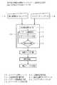
図2は本発明の実施の形態のマスクパターン評価方法及び補正方法を行うためのフロー図である。図2に示すように、光近接効果計算手段11、パターン領域設定手段12、ダミーパターン発生手段13及び光散乱計算手段14を備えたレイアウト発生ユニット10に、露光装置のPSFデータ15と近接効果を評価するマスクパターンデータ16を入力する。この場合の評価用のマスクパターンとしては、主に光近接効果を評価するものと、フレアの影響を評価するものが挙げられる。 FIG. 2 is a flowchart for performing the mask pattern evaluation method and the correction method according to the embodiment of the present invention. As shown in FIG. 2, the PSF data 15 and the proximity effect of the exposure apparatus are added to the
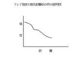
また、露光装置のPSFデータ15は、図3に示すように縮小光学系のミラーラフネスとミラーの焦点距離等の幾何学的設計値から算出し、距離と散乱量の関係を離散的な数値により表現する。なお、露光装置のPSFデータ15を簡易化させ、例えば、ガウシアン関数、フラクタル関数、線形近似関数、さらには、これら複数の関数の組み合わせで近似させることも可能である。 Further, as shown in FIG. 3, the PSF data 15 of the exposure apparatus is calculated from geometric design values such as the mirror roughness of the reduction optical system and the focal length of the mirror, and the relationship between the distance and the scattering amount is expressed by discrete numerical values. Express. Note that the PSF data 15 of the exposure apparatus can be simplified and approximated by, for example, a Gaussian function, a fractal function, a linear approximation function, or a combination of these functions.
入力されたマスクパターンデータ16をもとに、被露光基板、即ち、ウェーハ上に形成される光近接効果の空間像およびレジスト特性を光近接効果計算手段11により形成する。次いで、光近接効果の計算結果を考慮しパターン領域設定手段12によりマスクパターンデータ16をもとに評価用のマスクパターンを配置するパターン領域を設定する。さらに、ダミーパターン発生手段13により評価用のマスクパターンの周辺にマスクパターン被覆率を調整するダミーマスクパターンを発生させる。 Based on the input mask pattern data 16, the optical proximity effect calculation means 11 forms an aerial image and resist characteristics of the optical proximity effect formed on the substrate to be exposed, that is, the wafer. Next, in consideration of the calculation result of the optical proximity effect, the pattern region setting unit 12 sets a pattern region in which a mask pattern for evaluation is arranged based on the mask pattern data 16. Further, the dummy pattern generating means 13 generates a dummy mask pattern for adjusting the mask pattern coverage ratio around the mask pattern for evaluation.
次いで、光散乱計算手段14により、露光装置のPSFデータ15、マスクパターン領域内に配置された評価用のマスクパターン及びダミーマスクパターンを基に、ウェーハ上の任意の点における散乱光を計算する。この場合、散乱光の強度が所望の値、つまり、前記評価用のマスクパターンにおける散乱光が、任意の評価用のマスクパターンにおいて等しくなるように、フィードバックしながらパターン領域の設定をするとともにダミーマスクパターンを発生させて、評価用のマスクパターンを最適化させる。 Next, the scattered light at an arbitrary point on the wafer is calculated by the light scattering calculation means 14 based on the PSF data 15 of the exposure apparatus, the evaluation mask pattern and the dummy mask pattern arranged in the mask pattern region. In this case, the pattern area is set while feeding back and the dummy mask so that the scattered light intensity has a desired value, that is, the scattered light in the mask pattern for evaluation becomes equal in any mask pattern for evaluation. A pattern is generated to optimize the mask pattern for evaluation.
次いで、最適化させたマスクパターンを用いて検査用マスクを作成する。この検査用マスクを用いた露光結果を評価する。この時、検査用マスクに形成したマスクパターンをウェーハ上に投影して投影光強度分布を測定し、マスクパターンにおける散乱光強度分布を算出する。 Next, an inspection mask is created using the optimized mask pattern. The exposure result using this inspection mask is evaluated. At this time, the mask pattern formed on the inspection mask is projected onto the wafer, the projected light intensity distribution is measured, and the scattered light intensity distribution in the mask pattern is calculated.
次いで、算出した投影光強度分布と散乱光強度分布に基づき設計マスクパターンを複数の域に分割し、設計マスクパターンをウェーハ上に設けた転写レジストパターンの寸法が予め定めた値の範囲内となるよう補正する。 Next, the design mask pattern is divided into a plurality of areas based on the calculated projection light intensity distribution and scattered light intensity distribution, and the dimensions of the transfer resist pattern provided on the wafer are within a predetermined value range. Correct as follows.
以上を前提として、次に、図4乃至図8を参照して、本発明の実施例1のマスクパターン評価方法及び補正方法を説明する。まず、光近接効果を評価するマスクパターンの作成手法を説明する。図4は、光近接効果評価用のマスクパターンの一例を示す平面図である。 Based on the above, the mask pattern evaluation method and correction method according to the first embodiment of the present invention will now be described with reference to FIGS. First, a method for creating a mask pattern for evaluating the optical proximity effect will be described. FIG. 4 is a plan view showing an example of a mask pattern for evaluating the optical proximity effect.
図4に示すように、光が透過する開口部パターン21aの寸法は一定とし、未開口マスクパターン21bの寸法を変化させたL&Sパターンからなるマスクパターンを複数作成する。例えば、一例を挙げるとピッチが60nm〜200nmの間で所定間隔で変化するマスクパターンを10通り程度作成する。As shown in FIG. 4, the dimension of the
次いで、ウェーハ上に作成したマスクパターンをパターン転写することで、ピッチ依存性と呼ばれる評価を行う。なお、光近接効果評価用のマスクパターンは、ピッチ依存性評価以外に、マスク開口部寸法を変化させるパターンリニアリティや、2 次元パターンにおけるパターンコーナーの丸まり等がある。なお、矩形パターンでも短いパターンは先端部のコーナーの丸まりが問題となるので2次元パターンとなる。 Next, an evaluation called pitch dependency is performed by pattern transfer of the mask pattern created on the wafer. In addition to the pitch dependence evaluation, the mask pattern for evaluating the optical proximity effect includes, for example, pattern linearity that changes the size of the mask opening, and rounding of the pattern corner in the two-dimensional pattern. Note that even a rectangular pattern is a two-dimensional pattern because a short pattern has a problem of rounded corners at the tip.
これらは、露光波長ならびに露光装置の開口率やシグマ値等の光学条件により主に決定される回折効果の影響でウェーハ上寸法変化が予想されるものがある。つまり、近接効果評価用のパターン領域20のサイズ20a, 20b は、少なくとも、上述の光近接効果の計算において、光の回折の影響を受けなくなる領域より広くマスクパターン領域を設定することが必要となる。Some of these are expected to undergo dimensional changes on the wafer due to the influence of the diffraction effect mainly determined by the exposure wavelength and optical conditions such as the aperture ratio and sigma value of the exposure apparatus. In other words, the
例えば、露光波長13.5nm、開口率0.25、シグマ値0.7の露光条件において、L&Sパターンからなるマスクパターンを、開口部パターン21aの寸法を32nmで固定して、未開口部マスクパターン21bを変化させ、光リソグラフィシミュレーションにより空間像を求める。For example, under an exposure condition of an exposure wavelength of 13.5 nm, an aperture ratio of 0.25, and a sigma value of 0.7, a mask pattern composed of an L & S pattern is fixed ata size of the
図5は、予め設定した閾値におけるウェーハ上寸法CD(Critical Dimension)及びNILS(Normalized Image Log Slope)の算出結果である。なお、NILSとは露光余裕度を示す指標であり、投影光強度分布の立ち上がり部及び立ち下がり部の傾斜を光強度の対数と位置の対数の比で表したILSを規格化したものである。 FIG. 5 shows calculation results of on-wafer dimension CD (Critical Dimension) and NILS (Normalized Image Log Slope) at a preset threshold value. NILS is an index indicating the exposure margin and is a standardized ILS in which the slope of the rising and falling portions of the projection light intensity distribution is expressed by the ratio of the logarithm of the light intensity to the logarithm of the position.
図5に示すように、150nm程度のピッチで寸法変化がなくなるため、光近接効果の影響をなくすためには開口部パターン21aは互いに150nm以上離す必要がある。したがって、図4に示したマスクパターン領域20のサイズ20a,20bは少なくとも、2倍の300nm程度必要となることがわかる。当然ながら、マスクパターン寸法や露光波長ならびに露光装置の光学条件により、光近接効果が与える距離は異なるので、所望するパターンサイズや利用する露光装置および光学条件に応じて、もっとも小さくできるマスクパターン領域を判定することになる。As shown in FIG. 5, since the dimensional change is eliminated at a pitch of approximately 150nm, in order to eliminate the influence of the optical proximity
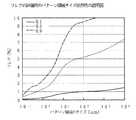
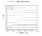
一方で、評価用のマスクパターン領域20のサイズ20a,20bを広げていくと、実質マスクパターンの開口部が増加し、ウェーハ上における散乱光の強度が増加する問題がある。図6は、フレア量のマスクパターン領域サイズ依存性の説明図である。ここでは、パターン開口率が0.1,0.5,0.9の正方形の評価用のマスクパターンにおいて、マスクパターン領域20のサイズ20a,20bを変化させた場合の、ウェーハ上に散乱してくる光強度を予め計算した露光装置のPSFデータを基に計算した結果を示した。On the other hand, when the
図6から明らかなように、パターンの開口率が大きくなるに従いフレア量は増加する傾向にあることがわかる。例えば、評価用のマスクパターン領域20が50μm角の場合、パターンの開口率が0.9(=90%)のときフレア量は9%以上となる。したがって、パターンの開口率によらずに精度の高い評価を行うためには、フレア量がほぼ等しい評価用のマスクパターン領域20で行う必要がある。例えば、評価用のマスクパターン領域20のサイズ20a,20bを1μm角以下として光近接効果の評価を行う。As can be seen from FIG. 6, the flare amount tends to increase as the aperture ratio of the pattern increases. For example, when the
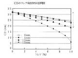
次に、フレア量による寸法変化を、13.5nm、開口率0.25、シグマ値0.7の露光条件を用い空間像を計算し、また、レジストの影響を空間像に対しガウシアン関数で畳み込み計算により予測を行った。 Next, the aerial image is calculated by using the exposure conditions of 13.5 nm, aperture ratio 0.25, and sigma value 0.7, and the influence of resist is convoluted with the Gaussian function on the aerial image. Prediction was made by calculation.
図7は寸法CDのフレア量依存性の説明図であり、ガウシアン関数の標準偏差(σ)を変数とした場合の計算結果を示したものである。ここでは、σ=0nm、5nm、10nm、15nmの4つの場合を示している。 FIG. 7 is an explanatory diagram of the flare amount dependency of the dimension CD, and shows the calculation result when the standard deviation (σ) of the Gaussian function is used as a variable. Here, four cases of σ = 0 nm, 5 nm, 10 nm, and 15 nm are shown.
この標準偏差の値σは、レジストの特性により変化するが、現在、使用しているレジストの特性は、ガウシアンの標準偏差(σ)で9nm程度であることがわかっている。つまり、フレアが10%程度存在し、標準偏差の値σを10nmとすると、ウェーハ上寸法はフレアが0%の時の32nmから右端の19nmに変化し、寸法変化量としては13nm(=32nm−19nm)程度であることがわかる。 Although the standard deviation value σ varies depending on the resist characteristics, it is known that the resist characteristics currently used are about 9 nm in terms of Gaussian standard deviation (σ). In other words, if flare exists about 10% and the standard deviation value σ is 10 nm, the dimension on the wafer changes from 32 nm when the flare is 0% to 19 nm on the right end, and the dimensional change is 13 nm (= 32 nm− 19 nm).
そこで、フレアによる寸法変動の影響がない状態で光近接効果の評価を行うためには、例えば、フレアによる影響を半導体装置に要求される最小寸法の10%以下に制御する評価用のマスクパターンを作成することが望まれる。例えば、ウェーハ上に形成するパターン寸法が32nmを目標とする場合、フレアの影響による寸法変化量は10%の3.2nm以下に制御する必要がある。 Therefore, in order to evaluate the optical proximity effect in the state where there is no influence of dimensional variation due to flare, for example, an evaluation mask pattern for controlling the influence of flare to 10% or less of the minimum dimension required for the semiconductor device is used. It is desirable to create. For example, when the pattern size formed on the wafer is 32 nm as a target, the dimensional change due to the flare needs to be controlled to 10% of 3.2 nm or less.
前述のようにフレアが10%であると、転写パターンの寸法CDは13nm変化することから、寸法変化を3.2nmに制御するには、フレアの変化量は、2.5%以下にすることが望まれ、フレア許容値と定義できる。 As described above, when the flare is 10%, the dimension CD of the transfer pattern changes by 13 nm. Therefore, in order to control the dimensional change to 3.2 nm, the flare change amount should be 2.5% or less. Can be defined as a flare tolerance.
このように散乱光計算において許容フレア量を定義すると、開口率が0.9の場合においても、図6から明らかなように評価用のマスクパターン領域20は0.7μm以下に設定することで寸法変動を所望の値とすることができる。なお、許容フレア量を超えた場合は、マスクパターン領域20を再設定するともに、ダミーマスクパターンを発生させてマスクパターンの被覆率が変化しないように調整して、所望の散乱光強度にすることも可能である。 Thus, when the allowable flare amount is defined in the scattered light calculation, even when the aperture ratio is 0.9, the
また、評価用のマスクパターン領域20の設定は、正方形の領域に限るものではない。例えば、図3に示した光近接効果が影響する最小の距離をマスクパターン領域20のサイズ20aに設定し、評価マスクパターンの長さを長くし、評価用のマスクパターン領域20のサイズ21bを変数として取り扱うことも可能である。The setting of the
図8は、フレアのマスクパターン領域長さ依存性の説明図であり、ここでは評価用のマスクパターン領域20が正方形と同様の仮定において、マスクパターン領域のサイズ20aを0.3μmに固定し、マスクパターン領域20のサイズ20bを変化させた場合の散乱光から計算したフレア量を示している。この場合では、マスクパターン領域20のサイズ20bを100μm以上の領域としても、評価マスクパターンの開口率が0.1から0.9まで変化した場合にも、散乱光によるフレアの影響を低減した状態で光近接効果を評価するパターン作成が可能であることがわかる。Figure 8 is an explanatory view of the mask pattern region length dependence of the flare, wherein the
これは、特に、LER(Line Edge Roughness)と呼ばれるレジストパターンの局所的な寸法変化がある場合、例えば、パターンの長さ方向に数μmの長さで平均化することで、前記LERの影響を低減することが可能になり、光近接効果による影響を抽出するのに有効となる。 This is particularly true when there is a local dimensional change of the resist pattern called LER (Line Edge Roughness), for example, by averaging the length of the pattern in the length direction of several μm, thereby reducing the influence of the LER. It becomes possible to reduce, and it becomes effective in extracting the influence by an optical proximity effect.
また、露光対象となる半導体装置を構成する層、例えば、ゲート、コンタクト、配線層によって、典型的なパターン被覆率が存在している。例えば、配線層のパターン被覆率は0.1〜0.6であり、一方、ゲートのパターン被覆率は0.3〜0.7である。したがって、このような近接効果の評価では、それら各層の典型的なパターン開口率と同等な状態で光近接効果を評価するようにマスクパターン領域の周辺にダミーパターンを発生させてマスクパターンの開口率(被覆率)を最適に調整することも可能である。 Moreover, a typical pattern coverage is present depending on the layers constituting the semiconductor device to be exposed, such as gates, contacts, and wiring layers. For example, the pattern coverage of the wiring layer is 0.1 to 0.6, while the pattern coverage of the gate is 0.3 to 0.7. Therefore, in the evaluation of such proximity effect, a dummy pattern is generated around the mask pattern region so that the optical proximity effect is evaluated in a state equivalent to the typical pattern aperture ratio of each layer, and the aperture ratio of the mask pattern is It is also possible to optimally adjust (coverage).
一方で、評価用のマスクパターンとして、フレア評価用のマスクパターンを用いる場合も、上述の手法と同様に、評価用のマスクパターンによる光近接効果の影響を受けないようにマスクパターン領域の設定を行う。また、レイアウト発生ユニットによりパターン設定領域外の周辺のパターン開口率を変化させることで評価用のマスクパターンの作成が可能となる。 On the other hand, even when a flare evaluation mask pattern is used as the evaluation mask pattern, the mask pattern region is set so as not to be affected by the optical proximity effect due to the evaluation mask pattern, as in the above-described method. Do. Further, a mask pattern for evaluation can be created by changing the pattern opening ratio around the pattern setting area by the layout generation unit.
この場合、パターン設定領域外の周辺のパターン開口率を変化させる手段としては、周辺にダミーパターンを発生させる以外に、評価用のマスクパターン領域20を広くすることで、図6に示すようにフレア変化の影響を評価することも可能である。 In this case, as a means for changing the peripheral pattern aperture ratio outside the pattern setting area, in addition to generating a dummy pattern in the periphery, the
本発明の実施例1においては、光近接効果評価用のマスクパターンに必要な最低限の領域(300nm×300nm)の設定、および、許容寸法内となる許容フレア量の定義は、レイアウト発生ユニット内で計算している。しかし、レイアウト発生ユニット内で計算する他に、外部計算機において計算し、LANや記憶媒体を通じてレイアウト発生ユニットに取り込む手法、或いは、外部計算機の結果を入力する機構としても良い。 In the first embodiment of the present invention, the setting of the minimum area (300 nm × 300 nm) necessary for the mask pattern for evaluating the optical proximity effect and the definition of the allowable flare amount within the allowable dimensions are defined in the layout generation unit. It is calculated with. However, in addition to the calculation in the layout generation unit, a method of calculating in an external computer and importing into the layout generation unit through a LAN or a storage medium, or a mechanism for inputting the result of the external computer may be used.
このようなレイアウト発生ユニットを用いることで、半導体装置等の電子デバイス製造工程における寸法精度を向上させる補正テーブルの作成が容易となり、半導体装置の性能向上を図ることができる。 By using such a layout generation unit, it becomes easy to create a correction table that improves the dimensional accuracy in the manufacturing process of an electronic device such as a semiconductor device, and the performance of the semiconductor device can be improved.
また、上記の実施の形態及び実施例の説明においては、EUV光の波長を13.5nmとしているが、13.5nmに限られるものではなく、任意の波長を用いても良いものです。 In the description of the above embodiment and examples, the wavelength of the EUV light is 13.5 nm, but the wavelength is not limited to 13.5 nm, and any wavelength may be used.
ここで、実施例1を含む本発明の実施の形態に関して、以下の付記を開示する。
(付記1)
第1のマスクに複数の評価パターンを配置し、露光装置の投影光学系を介して結像する空間像の特性を計測し、第2のマスクに設ける実露光パターンの補正データを作成するマスクパターン評価方法であって、
前記投影光学系のミラーの特性から、被露光基板上に散乱される点像分布関数を算出する工程と、
前記点像分布関数と前記第1のマスク上に配置してある前記評価パターンの被覆率を畳み込むことにより任意の前記評価パターンにおけるフレア光強度を算出する工程と、
前記複数の評価パターンのパターン配置およびパターン領域を前記算出したフレア光強度が等しくなるよう設定し、前記設定に基づき前記第1のマスクを作製する工程と、
作製した前記第1のマスクに設けたパターンを前記被露光基板上に投影する工程と、
前記空間像の特性を計測する工程と、
前記計測結果を参照して補正データを作成する工程を
有することを特徴とするマスクパターン評価方法。
(付記2)
第1のマスクに複数の評価パターンおよび複数のダミーパターンを配置し、露光装置の投影光学系を介して結像する空間像の特性を計測し、第2のマスクに設ける実露光パターンの補正データを作成するマスクパターン評価方法であって、
前記投影光学系のミラーの特性から、被露光基板上に散乱される点像分布関数を算出する工程と、
前記点像分布関数と前記第1のマスク上に配置してある前記評価パターンおよび前記ダミーパターンの被覆率を畳み込むことにより任意の前記評価パターンおよび前記ダミーパターンにおけるフレア光強度を算出する工程と、
前記複数の評価パターンおよび前記複数のダミーパターンのパターン配置およびパターン領域を、前記算出したフレア光強度が等しくなるよう設定し、前記設定に基づき前記第1のマスクを作製する工程と、
作製した前記第1のマスクに設けたパターンを前記被露光基板上に投影する工程と、
前記空間像の特性を計測する工程と、
前記計測結果を参照して補正データを作成する工程を
有することを特徴とするマスクパターン評価方法。
(付記3)
前記複数の評価パターンを、互いに150nm以上離れた位置に配置する工程と、
前記評価パターンにおけるフレア光強度が、前記評価パターンのパターン配置およびパターン領域が変化しても、複数の前記評価パターンにおけるフレア強度の差分が2%以下となるように前記パターン配置を設定する工程と
を有することを特徴とする付記1または付記2に記載のマスクパターン評価方法。
(付記4)
前記フレア光強度が露光対象に応じて前記点像分布関数から算出した中心値となるように、前記評価用のパターン領域のサイズを設定するか或いは前記被覆率の異なるダミーパターンを配置することを特徴とする付記1乃至付記3のいずれか1に記載のマスクパターン評価方法。
(付記5)
前記散乱される点像分布関数を、ガウシアン関数、フラクタル関数、線形近似関数または前記各関数の組み合わせで近似することを特徴とする付記1乃至付記4のいずれか1に記載のマスクパターン評価方法。
(付記6)
付記1乃至付記5のいずれか1に記載のマスクパターン評価方法より補正されたマスクパターンを検査用マスクに形成する工程と、
前記検査用マスクに形成したマスクパターンを被露光基板上に投影して投影光強度分布を測定し、前記マスクパターンにおける散乱光強度分布を算出する工程と、
設計マスクパターンを複数の領域に分割し、算出した前記投影光強度分布と前記散乱光強度分布に基づき、前記マスクパターンを前記被露光基板上に設けた転写レジストパターンの寸法が予め定めた値の範囲内となるよう補正する工程と
を有することを特徴とするマスクパターン補正方法。
(付記7)
第1のマスクに複数の評価パターンを配置する手段と、
点像分布関数と前記第1のマスク上に配置した評価パターンの被覆率を畳み込むことにより任意の前記評価パターンにおけるフレア光強度を算出する手段と、
前記算出したフレア光強度が等しくなるように複数の前記評価パターンのパターン領域を設定およびパターン配置を行う手段と
を有することを特徴とするマスクパターン発生装置。Here, regarding the embodiment of the present invention including Example 1, the following additional notes are disclosed.
(Appendix 1)
A mask pattern that arranges a plurality of evaluation patterns on the first mask, measures the characteristics of the aerial image formed through the projection optical system of the exposure apparatus, and creates correction data for the actual exposure pattern provided on the second mask An evaluation method,
A step of calculating a point spread function scattered on the substrate to be exposed from the characteristics of the mirror of the projection optical system;
Calculating a flare light intensity in any of the evaluation patterns by convolving the point spread function and the coverage of the evaluation pattern disposed on the first mask;
Setting the pattern arrangement and pattern area of the plurality of evaluation patterns so that the calculated flare light intensity is equal, and producing the first mask based on the setting;
Projecting a pattern provided on the produced first mask onto the substrate to be exposed;
Measuring the characteristics of the aerial image;
A mask pattern evaluation method comprising a step of creating correction data with reference to the measurement result.
(Appendix 2)
A plurality of evaluation patterns and a plurality of dummy patterns are arranged on the first mask, the characteristics of the aerial image formed through the projection optical system of the exposure apparatus are measured, and correction data of the actual exposure pattern provided on the second mask A mask pattern evaluation method for creating
A step of calculating a point spread function scattered on the substrate to be exposed from the characteristics of the mirror of the projection optical system;
Calculating a flare light intensity in any of the evaluation pattern and the dummy pattern by convolving the coverage of the evaluation pattern and the dummy pattern arranged on the point spread function and the first mask;
Setting the pattern arrangement and pattern area of the plurality of evaluation patterns and the plurality of dummy patterns so that the calculated flare light intensities are equal, and producing the first mask based on the settings;
Projecting a pattern provided on the produced first mask onto the substrate to be exposed;
Measuring the characteristics of the aerial image;
A step of creating correction data with reference to the measurement result
A mask pattern evaluation method comprising:
(Appendix3 )
Arranging the plurality of evaluation patterns at positions separated from each other by 150 nm or more;
Setting the pattern arrangement so that the difference in flare intensity in the plurality of evaluation patterns is 2% or less even if the flare light intensity in the evaluation pattern changes in the pattern arrangement and pattern area of the evaluation pattern; The mask pattern evaluation method accordingto
(Appendix 4)
The size of the pattern area for evaluation is set or a dummy pattern having a different coverage is disposed so that the flare light intensity becomes the center value calculated from the point spread function according to the exposure target. The mask pattern evaluation method according to any one of
(Appendix 5)
The mask pattern evaluation method according to any one of
(Appendix 6)
Forming a mask pattern corrected by the mask pattern evaluation method according to any one of
Projecting a mask pattern formed on the inspection mask onto an exposure substrate to measure a projected light intensity distribution, and calculating a scattered light intensity distribution in the mask pattern;
A design mask pattern is divided into a plurality of regions, and based on the calculated projection light intensity distribution and the scattered light intensity distribution, the dimension of a transfer resist pattern in which the mask pattern is provided on the substrate to be exposed has a predetermined value. And a step of correcting the mask pattern so as to be within the range.
(Appendix 7)
Means for arranging a plurality of evaluation patterns on the first mask;
Means for calculating a flare light intensity in an arbitrary evaluation pattern by convolving apoint spread function and a coverage of the evaluation pattern arranged on the first mask;
A mask pattern generation apparatus comprising: means for setting and arranging pattern areas of the plurality of evaluation patterns so that the calculated flare light intensities are equal.
1 光源
2 照明光学系
3 レチクルステージ
4 投影光学系
5 被露光基板
6 ウェーハステージ
10 レイアウト発生ユニット
11 光近接効果計算手段
12 パターン領域設定手段
13 ダミーパターン発生手段
14 光散乱計算手段
15 露光装置のPSFデータ
16 マスクパターンデータ
20 マスクパターン領域
20a,20b マスクパターン領域のサイズ
21a 開口部パターン
21b 未開口マスクパターンDESCRIPTION OF
Claims (5)
Translated fromJapanese前記投影光学系のミラーの特性から、被露光基板上に散乱される点像分布関数を算出する工程と、
前記点像分布関数と前記第1のマスク上に配置してある前記評価パターンの被覆率を畳み込むことにより任意の前記評価パターンにおけるフレア光強度を算出する工程と、
前記複数の評価パターンのパターン配置およびパターン領域を前記算出したフレア光強度が等しくなるよう設定し、前記設定に基づき前記第1のマスクを作製する工程と、
作製した前記第1のマスクに設けたパターンを前記被露光基板上に投影する工程と、
前記空間像の特性を計測する工程と、
前記計測結果を参照して補正データを作成する工程を
有することを特徴とするマスクパターン評価方法。A mask pattern that arranges a plurality of evaluation patterns on the first mask, measures the characteristics of the aerial image formed through the projection optical system of the exposure apparatus, and creates correction data for the actual exposure pattern provided on the second mask An evaluation method,
A step of calculating a point spread function scattered on the substrate to be exposed from the characteristics of the mirror of the projection optical system;
Calculating a flare light intensity in any of the evaluation patterns by convolving the point spread function and the coverage of the evaluation pattern disposed on the first mask;
Setting the pattern arrangement and pattern area of the plurality of evaluation patterns so that the calculated flare light intensity is equal, and producing the first mask based on the setting;
Projecting a pattern provided on the produced first mask onto the substrate to be exposed;
Measuring the characteristics of the aerial image;
A mask pattern evaluation method comprising a step of creating correction data with reference to the measurement result.
前記投影光学系のミラーの特性から、被露光基板上に散乱される点像分布関数を算出する工程と、A step of calculating a point spread function scattered on the substrate to be exposed from the characteristics of the mirror of the projection optical system;
前記点像分布関数と前記第1のマスク上に配置してある前記評価パターンおよび前記ダミーパターンの被覆率を畳み込むことにより任意の前記評価パターンおよび前記ダミーパターンにおけるフレア光強度を算出する工程と、Calculating a flare light intensity in any of the evaluation pattern and the dummy pattern by convolving the coverage of the evaluation pattern and the dummy pattern arranged on the point spread function and the first mask;
前記複数の評価パターンおよび前記複数のダミーパターンのパターン配置およびパターン領域を、前記算出したフレア光強度が等しくなるよう設定し、前記設定に基づき前記第1のマスクを作製する工程と、Setting the pattern arrangement and pattern area of the plurality of evaluation patterns and the plurality of dummy patterns so that the calculated flare light intensities are equal, and producing the first mask based on the settings;
作製した前記第1のマスクに設けたパターンを前記被露光基板上に投影する工程と、Projecting a pattern provided on the produced first mask onto the substrate to be exposed;
前記空間像の特性を計測する工程と、Measuring the characteristics of the aerial image;
前記計測結果を参照して補正データを作成する工程をA step of creating correction data with reference to the measurement result
有することを特徴とするマスクパターン評価方法。A mask pattern evaluation method comprising:
前記評価パターンにおけるフレア光強度が、前記評価パターンのパターン配置およびパターン領域が変化しても、複数の前記評価パターンにおけるフレア強度の差分が2%以下となるように前記パターン配置を設定する工程と
を有することを特徴とする請求項1または請求項2に記載のマスクパターン評価方法。Arranging the plurality of evaluation patterns at positions separated from each other by 150 nm or more;
Setting the pattern arrangement so that the difference in flare intensity in the plurality of evaluation patterns is 2% or less even if the flare light intensity in the evaluation pattern changes in the pattern arrangement and pattern area of the evaluation pattern; mask pattern evaluation method accordingto claim 1or claim2,characterized in that it has a.
前記検査用マスクに形成したマスクパターンを被露光基板上に投影して投影光強度分布を測定し、前記マスクパターンにおける散乱光強度分布を算出する工程と、
設計マスクパターンを複数の領域に分割し、算出した前記投影光強度分布と前記散乱光強度分布に基づき、前記マスクパターンを前記被露光基板上に設けた転写レジストパターンの寸法が予め定めた値の範囲内となるよう補正する工程と
を有することを特徴とするマスクパターン補正方法。Forming a mask pattern corrected by the mask pattern evaluation method according to any one of claims 1 to 3 on an inspection mask;
Projecting a mask pattern formed on the inspection mask onto an exposure substrate to measure a projected light intensity distribution, and calculating a scattered light intensity distribution in the mask pattern;
A design mask pattern is divided into a plurality of regions, and based on the calculated projection light intensity distribution and the scattered light intensity distribution, the dimension of a transfer resist pattern in which the mask pattern is provided on the substrate to be exposed has a predetermined value. And a step of correcting the mask pattern so as to be within the range.
点像分布関数と前記第1のマスク上に配置した評価パターンの被覆率を畳み込むことにより任意の前記評価パターンにおけるフレア光強度を算出する手段と、
前記算出したフレア光強度が等しくなるように複数の前記評価パターンのパターン領域を設定およびパターン配置を行う手段と
を有することを特徴とするマスクパターン発生装置。Means for arranging a plurality of evaluation patterns on the first mask;
Means for calculating a flare light intensity in an arbitrary evaluation pattern by convolving apoint spread function and a coverage of the evaluation pattern arranged on the first mask;
A mask pattern generation apparatus comprising: means for setting and arranging pattern areas of the plurality of evaluation patterns so that the calculated flare light intensities are equal.
Priority Applications (1)
| Application Number | Priority Date | Filing Date | Title |
|---|---|---|---|
| JP2009167386AJP5407623B2 (en) | 2009-07-16 | 2009-07-16 | Mask pattern evaluation method, mask pattern correction method, and mask pattern generator |
Applications Claiming Priority (1)
| Application Number | Priority Date | Filing Date | Title |
|---|---|---|---|
| JP2009167386AJP5407623B2 (en) | 2009-07-16 | 2009-07-16 | Mask pattern evaluation method, mask pattern correction method, and mask pattern generator |
Publications (2)
| Publication Number | Publication Date |
|---|---|
| JP2011023549A JP2011023549A (en) | 2011-02-03 |
| JP5407623B2true JP5407623B2 (en) | 2014-02-05 |
Family
ID=43633356
Family Applications (1)
| Application Number | Title | Priority Date | Filing Date |
|---|---|---|---|
| JP2009167386AExpired - Fee RelatedJP5407623B2 (en) | 2009-07-16 | 2009-07-16 | Mask pattern evaluation method, mask pattern correction method, and mask pattern generator |
Country Status (1)
| Country | Link |
|---|---|
| JP (1) | JP5407623B2 (en) |
Families Citing this family (4)
| Publication number | Priority date | Publication date | Assignee | Title |
|---|---|---|---|---|
| US8443308B2 (en)* | 2011-05-02 | 2013-05-14 | Synopsys Inc. | EUV lithography flare calculation and compensation |
| JP2013062433A (en) | 2011-09-14 | 2013-04-04 | Toshiba Corp | Pattern generating method, pattern formation method, and pattern generation program |
| JP2013125906A (en) | 2011-12-15 | 2013-06-24 | Toshiba Corp | Flare map calculation method, flare map calculation program, and method of manufacturing semiconductor device |
| CN111903120A (en)* | 2018-03-29 | 2020-11-06 | 索尼公司 | Signal processing device, information processing method, and program |
Family Cites Families (7)
| Publication number | Priority date | Publication date | Assignee | Title |
|---|---|---|---|---|
| SG144749A1 (en)* | 2002-03-25 | 2008-08-28 | Asml Masktools Bv | Method and apparatus for decomposing semiconductor device patterns into phase and chrome regions for chromeless phase lithography |
| JP2004126486A (en)* | 2002-07-31 | 2004-04-22 | Fujitsu Ltd | Pattern dimension correction device and pattern dimension correction method |
| JP4190227B2 (en)* | 2002-07-31 | 2008-12-03 | 富士通マイクロエレクトロニクス株式会社 | Photomask, method for designing the same, and method for manufacturing a semiconductor device using the same |
| JP4329333B2 (en)* | 2002-11-13 | 2009-09-09 | ソニー株式会社 | Exposure mask correction method |
| JP2004205833A (en)* | 2002-12-25 | 2004-07-22 | Fujitsu Ltd | Photomask and pattern forming method |
| US7234130B2 (en)* | 2004-02-25 | 2007-06-19 | James Word | Long range corrections in integrated circuit layout designs |
| US7713665B2 (en)* | 2006-03-29 | 2010-05-11 | Asml Netherlands B.V. | Lithographic apparatus and patterning device |
- 2009
- 2009-07-16JPJP2009167386Apatent/JP5407623B2/ennot_activeExpired - Fee Related
Also Published As
| Publication number | Publication date |
|---|---|
| JP2011023549A (en) | 2011-02-03 |
Similar Documents
| Publication | Publication Date | Title |
|---|---|---|
| KR101527496B1 (en) | Lithography model for 3D resist profile simulation | |
| KR100719154B1 (en) | Method of optical proximity correction design for contact hole mask | |
| KR101757743B1 (en) | Flare correction method and method for fabricating EUV(Extreme Ultra Violet) mask | |
| JP4707701B2 (en) | Method and computer program for generating a model for simulating the imaging performance of an optical imaging system having a pupil | |
| KR102444680B1 (en) | Binarization method and preform mask optimization flow | |
| TWI639897B (en) | Modeling post-exposure processes | |
| US7327436B2 (en) | Method for evaluating a local flare, correction method for a mask pattern, manufacturing method for a semiconductor device and a computer program product | |
| KR20060087446A (en) | Methods, programs, and apparatus for improving the calibration of resist models used for critical dimension calculation | |
| JP2008166777A (en) | Lithographic device and method of manufacturing device | |
| JP4398852B2 (en) | Method for adjusting mask pattern transmittance to improve process latitude | |
| US20200249578A1 (en) | Method and apparatus for source mask optimization configured to increase scanner throughput for a patterning process | |
| KR102063229B1 (en) | Simulation of Lithography Using Multi-Sampling of Angle Distribution of Source Radiation | |
| KR101437575B1 (en) | Substrate-topography-aware lithography modeling | |
| KR20190005986A (en) | Displacement-based overlay or alignment | |
| KR20200109372A (en) | Systems and methods to improve resist model predictions | |
| JP5407623B2 (en) | Mask pattern evaluation method, mask pattern correction method, and mask pattern generator | |
| CN112424694A (en) | Using pattern recognition to automatically improve SEM profile measurement accuracy and stability | |
| KR20180100367A (en) | Etch-assist features | |
| JP2008159788A (en) | Exposure condition calculation program and exposure condition calculation method | |
| TWI687781B (en) | Systems and methods for reducing resist model prediction errors | |
| US20250189881A1 (en) | Lithographic pattern representation with curvilinear elements | |
| CN120359467A (en) | Source mask optimization based on systematic effects on lithographic apparatus | |
| CN119343632A (en) | Stochastically Aware Source Mask Optimization Based on Probabilistic Distribution of Edge Placement | |
| TW202109347A (en) | Method and system for reducing layout distortion due to exposure non-uniformity | |
| TWI842639B (en) | Method and system for enhancing target features of a pattern imaged onto a substrate |
Legal Events
| Date | Code | Title | Description |
|---|---|---|---|
| RD03 | Notification of appointment of power of attorney | Free format text:JAPANESE INTERMEDIATE CODE: A7423 Effective date:20110915 | |
| A621 | Written request for application examination | Free format text:JAPANESE INTERMEDIATE CODE: A621 Effective date:20120405 | |
| A977 | Report on retrieval | Free format text:JAPANESE INTERMEDIATE CODE: A971007 Effective date:20130627 | |
| A131 | Notification of reasons for refusal | Free format text:JAPANESE INTERMEDIATE CODE: A131 Effective date:20130702 | |
| A521 | Written amendment | Free format text:JAPANESE INTERMEDIATE CODE: A523 Effective date:20130829 | |
| TRDD | Decision of grant or rejection written | ||
| A01 | Written decision to grant a patent or to grant a registration (utility model) | Free format text:JAPANESE INTERMEDIATE CODE: A01 Effective date:20131008 | |
| A61 | First payment of annual fees (during grant procedure) | Free format text:JAPANESE INTERMEDIATE CODE: A61 Effective date:20131021 | |
| R150 | Certificate of patent or registration of utility model | Ref document number:5407623 Country of ref document:JP Free format text:JAPANESE INTERMEDIATE CODE: R150 | |
| S531 | Written request for registration of change of domicile | Free format text:JAPANESE INTERMEDIATE CODE: R313531 | |
| R350 | Written notification of registration of transfer | Free format text:JAPANESE INTERMEDIATE CODE: R350 | |
| LAPS | Cancellation because of no payment of annual fees |