JP5401824B2 - Image display device - Google Patents
Image display deviceDownload PDFInfo
- Publication number
- JP5401824B2 JP5401824B2JP2008100879AJP2008100879AJP5401824B2JP 5401824 B2JP5401824 B2JP 5401824B2JP 2008100879 AJP2008100879 AJP 2008100879AJP 2008100879 AJP2008100879 AJP 2008100879AJP 5401824 B2JP5401824 B2JP 5401824B2
- Authority
- JP
- Japan
- Prior art keywords
- image display
- resin composition
- cured
- display device
- photocurable resin
- Prior art date
- Legal status (The legal status is an assumption and is not a legal conclusion. Google has not performed a legal analysis and makes no representation as to the accuracy of the status listed.)
- Active
Links
Images


Classifications
- G—PHYSICS
- G02—OPTICS
- G02F—OPTICAL DEVICES OR ARRANGEMENTS FOR THE CONTROL OF LIGHT BY MODIFICATION OF THE OPTICAL PROPERTIES OF THE MEDIA OF THE ELEMENTS INVOLVED THEREIN; NON-LINEAR OPTICS; FREQUENCY-CHANGING OF LIGHT; OPTICAL LOGIC ELEMENTS; OPTICAL ANALOGUE/DIGITAL CONVERTERS
- G02F1/00—Devices or arrangements for the control of the intensity, colour, phase, polarisation or direction of light arriving from an independent light source, e.g. switching, gating or modulating; Non-linear optics
- G02F1/01—Devices or arrangements for the control of the intensity, colour, phase, polarisation or direction of light arriving from an independent light source, e.g. switching, gating or modulating; Non-linear optics for the control of the intensity, phase, polarisation or colour
- G02F1/13—Devices or arrangements for the control of the intensity, colour, phase, polarisation or direction of light arriving from an independent light source, e.g. switching, gating or modulating; Non-linear optics for the control of the intensity, phase, polarisation or colour based on liquid crystals, e.g. single liquid crystal display cells
- G02F1/133—Constructional arrangements; Operation of liquid crystal cells; Circuit arrangements
- G02F1/1333—Constructional arrangements; Manufacturing methods
- G02F1/133308—Support structures for LCD panels, e.g. frames or bezels
- G—PHYSICS
- G02—OPTICS
- G02B—OPTICAL ELEMENTS, SYSTEMS OR APPARATUS
- G02B1/00—Optical elements characterised by the material of which they are made; Optical coatings for optical elements
- G02B1/10—Optical coatings produced by application to, or surface treatment of, optical elements
- G—PHYSICS
- G02—OPTICS
- G02B—OPTICAL ELEMENTS, SYSTEMS OR APPARATUS
- G02B1/00—Optical elements characterised by the material of which they are made; Optical coatings for optical elements
- G02B1/10—Optical coatings produced by application to, or surface treatment of, optical elements
- G02B1/11—Anti-reflection coatings
- G—PHYSICS
- G02—OPTICS
- G02B—OPTICAL ELEMENTS, SYSTEMS OR APPARATUS
- G02B1/00—Optical elements characterised by the material of which they are made; Optical coatings for optical elements
- G02B1/10—Optical coatings produced by application to, or surface treatment of, optical elements
- G02B1/14—Protective coatings, e.g. hard coatings
- G—PHYSICS
- G02—OPTICS
- G02F—OPTICAL DEVICES OR ARRANGEMENTS FOR THE CONTROL OF LIGHT BY MODIFICATION OF THE OPTICAL PROPERTIES OF THE MEDIA OF THE ELEMENTS INVOLVED THEREIN; NON-LINEAR OPTICS; FREQUENCY-CHANGING OF LIGHT; OPTICAL LOGIC ELEMENTS; OPTICAL ANALOGUE/DIGITAL CONVERTERS
- G02F1/00—Devices or arrangements for the control of the intensity, colour, phase, polarisation or direction of light arriving from an independent light source, e.g. switching, gating or modulating; Non-linear optics
- G02F1/01—Devices or arrangements for the control of the intensity, colour, phase, polarisation or direction of light arriving from an independent light source, e.g. switching, gating or modulating; Non-linear optics for the control of the intensity, phase, polarisation or colour
- G02F1/13—Devices or arrangements for the control of the intensity, colour, phase, polarisation or direction of light arriving from an independent light source, e.g. switching, gating or modulating; Non-linear optics for the control of the intensity, phase, polarisation or colour based on liquid crystals, e.g. single liquid crystal display cells
- G02F1/133—Constructional arrangements; Operation of liquid crystal cells; Circuit arrangements
- G02F1/1333—Constructional arrangements; Manufacturing methods
- G02F1/133308—Support structures for LCD panels, e.g. frames or bezels
- G02F1/133311—Environmental protection, e.g. against dust or humidity
- G—PHYSICS
- G02—OPTICS
- G02F—OPTICAL DEVICES OR ARRANGEMENTS FOR THE CONTROL OF LIGHT BY MODIFICATION OF THE OPTICAL PROPERTIES OF THE MEDIA OF THE ELEMENTS INVOLVED THEREIN; NON-LINEAR OPTICS; FREQUENCY-CHANGING OF LIGHT; OPTICAL LOGIC ELEMENTS; OPTICAL ANALOGUE/DIGITAL CONVERTERS
- G02F1/00—Devices or arrangements for the control of the intensity, colour, phase, polarisation or direction of light arriving from an independent light source, e.g. switching, gating or modulating; Non-linear optics
- G02F1/01—Devices or arrangements for the control of the intensity, colour, phase, polarisation or direction of light arriving from an independent light source, e.g. switching, gating or modulating; Non-linear optics for the control of the intensity, phase, polarisation or colour
- G02F1/13—Devices or arrangements for the control of the intensity, colour, phase, polarisation or direction of light arriving from an independent light source, e.g. switching, gating or modulating; Non-linear optics for the control of the intensity, phase, polarisation or colour based on liquid crystals, e.g. single liquid crystal display cells
- G02F1/133—Constructional arrangements; Operation of liquid crystal cells; Circuit arrangements
- G02F1/1333—Constructional arrangements; Manufacturing methods
- G02F1/133308—Support structures for LCD panels, e.g. frames or bezels
- G02F1/133331—Cover glasses
- G—PHYSICS
- G09—EDUCATION; CRYPTOGRAPHY; DISPLAY; ADVERTISING; SEALS
- G09F—DISPLAYING; ADVERTISING; SIGNS; LABELS OR NAME-PLATES; SEALS
- G09F9/00—Indicating arrangements for variable information in which the information is built-up on a support by selection or combination of individual elements
- G09F9/30—Indicating arrangements for variable information in which the information is built-up on a support by selection or combination of individual elements in which the desired character or characters are formed by combining individual elements
- G09F9/35—Indicating arrangements for variable information in which the information is built-up on a support by selection or combination of individual elements in which the desired character or characters are formed by combining individual elements being liquid crystals
- G—PHYSICS
- G02—OPTICS
- G02F—OPTICAL DEVICES OR ARRANGEMENTS FOR THE CONTROL OF LIGHT BY MODIFICATION OF THE OPTICAL PROPERTIES OF THE MEDIA OF THE ELEMENTS INVOLVED THEREIN; NON-LINEAR OPTICS; FREQUENCY-CHANGING OF LIGHT; OPTICAL LOGIC ELEMENTS; OPTICAL ANALOGUE/DIGITAL CONVERTERS
- G02F2201/00—Constructional arrangements not provided for in groups G02F1/00 - G02F7/00
- G02F2201/08—Constructional arrangements not provided for in groups G02F1/00 - G02F7/00 light absorbing layer
- G02F2201/086—UV absorbing
- G—PHYSICS
- G02—OPTICS
- G02F—OPTICAL DEVICES OR ARRANGEMENTS FOR THE CONTROL OF LIGHT BY MODIFICATION OF THE OPTICAL PROPERTIES OF THE MEDIA OF THE ELEMENTS INVOLVED THEREIN; NON-LINEAR OPTICS; FREQUENCY-CHANGING OF LIGHT; OPTICAL LOGIC ELEMENTS; OPTICAL ANALOGUE/DIGITAL CONVERTERS
- G02F2201/00—Constructional arrangements not provided for in groups G02F1/00 - G02F7/00
- G02F2201/50—Protective arrangements
- G—PHYSICS
- G02—OPTICS
- G02F—OPTICAL DEVICES OR ARRANGEMENTS FOR THE CONTROL OF LIGHT BY MODIFICATION OF THE OPTICAL PROPERTIES OF THE MEDIA OF THE ELEMENTS INVOLVED THEREIN; NON-LINEAR OPTICS; FREQUENCY-CHANGING OF LIGHT; OPTICAL LOGIC ELEMENTS; OPTICAL ANALOGUE/DIGITAL CONVERTERS
- G02F2202/00—Materials and properties
- G02F2202/02—Materials and properties organic material
- G02F2202/022—Materials and properties organic material polymeric
- G02F2202/023—Materials and properties organic material polymeric curable
- G—PHYSICS
- G02—OPTICS
- G02F—OPTICAL DEVICES OR ARRANGEMENTS FOR THE CONTROL OF LIGHT BY MODIFICATION OF THE OPTICAL PROPERTIES OF THE MEDIA OF THE ELEMENTS INVOLVED THEREIN; NON-LINEAR OPTICS; FREQUENCY-CHANGING OF LIGHT; OPTICAL LOGIC ELEMENTS; OPTICAL ANALOGUE/DIGITAL CONVERTERS
- G02F2202/00—Materials and properties
- G02F2202/28—Adhesive materials or arrangements
Landscapes
- Physics & Mathematics (AREA)
- General Physics & Mathematics (AREA)
- Nonlinear Science (AREA)
- Optics & Photonics (AREA)
- Chemical & Material Sciences (AREA)
- Crystallography & Structural Chemistry (AREA)
- Mathematical Physics (AREA)
- Engineering & Computer Science (AREA)
- Theoretical Computer Science (AREA)
- Ecology (AREA)
- Life Sciences & Earth Sciences (AREA)
- Biodiversity & Conservation Biology (AREA)
- Health & Medical Sciences (AREA)
- Environmental & Geological Engineering (AREA)
- Environmental Sciences (AREA)
- Toxicology (AREA)
- Devices For Indicating Variable Information By Combining Individual Elements (AREA)
- Liquid Crystal (AREA)
- Polymerisation Methods In General (AREA)
- Compositions Of Macromolecular Compounds (AREA)
- Graft Or Block Polymers (AREA)
- Polyurethanes Or Polyureas (AREA)
- Addition Polymer Or Copolymer, Post-Treatments, Or Chemical Modifications (AREA)
- Macromonomer-Based Addition Polymer (AREA)
Description
Translated fromJapanese本発明は、例えば携帯電話等に用いられる液晶表示装置(LCD)等の画像表示装置に関し、特に、画像表示部上に透明な保護部を設けた画像表示装置およびその製造方法に関する。 The present invention relates to an image display device such as a liquid crystal display (LCD) used in, for example, a mobile phone, and more particularly to an image display device in which a transparent protective part is provided on an image display part and a method for manufacturing the same.
従来、この種の表示装置としては、例えば図6に示す液晶表示装置101が知られている。この液晶表示装置101は、液晶表示パネル102上に、例えば、ガラスやプラスチックスからなる透明な保護部103を有している。 Conventionally, for example, a liquid
この場合、液晶表示パネル102表面及び偏光板(図示せず)を保護するため、保護部103との間にスペーサ104を介在させることによって液晶表示パネル102と保護部103との間に空隙105が設けられるようになっている。 In this case, in order to protect the surface of the liquid
しかし、液晶表示パネル102と保護部103との間の空隙105の存在により、光の散乱がおき、それに起因してコントラストや輝度が低下し、また空隙105の存在はパネルの薄型化の妨げとなっている。 However, the presence of the
このような間題に鑑み、液晶表示パネルと保護部との間の空隙に樹脂を充填することも提案されているが(例えば特許文献1)、樹脂硬化物の硬化収縮の際の応力によって液晶表示パネルの液晶を挟持する光学ガラス板に変形が生じ、液晶材料の配向乱れ等の表示不良の原因となっている。 In view of such problems, it has also been proposed to fill the gap between the liquid crystal display panel and the protective part with a resin (for example, Patent Document 1), but the liquid crystal is caused by the stress during curing shrinkage of the cured resin. Deformation occurs in the optical glass plate sandwiching the liquid crystal of the display panel, which causes display defects such as disordered alignment of the liquid crystal material.
また、液晶表示パネルと保護部との間の空隙に樹脂組成物を充填すると、製造条件等により、樹脂組成物がバックライト側に付着する不具合があった。
本発明は、このような従来の技術の課題を考慮してなされたもので、その目的とするところは、画像表示部の変形に起因する表示不良を生じさせず、高輝度及び高コントラストの画像表示が可能であり、加えてバックライト側に不要な樹脂が付着していない薄型の画像表示装置を提供することにある。 The present invention has been made in consideration of such problems of the conventional technology, and the object of the present invention is to produce a high-brightness and high-contrast image without causing display defects due to deformation of the image display unit. Another object of the present invention is to provide a thin image display device that can display and in which unnecessary resin does not adhere to the backlight side.
上記課題を解決するため、本発明は、画像表示部と該画像表示部を取り囲む枠体とを有する表示側パネルと、保護部との間に、光硬化型樹脂組成物を、画像表示部と枠体に亘るように介在させ、光硬化させて樹脂硬化物層を形成する工程を有する画像表示装置の製造方法であって、
光硬化型樹脂組成物として、粘度(25℃、コーンプレート型回転粘度計、コーンプレートのテーパ角度C35/2°、10rpm)が3000mPa・s以上12000mPa・s以下の樹脂組成物を使用する画像表示装置の製造方法を提供する。In order to solve the above-described problems, the present invention provides a photocurable resin composition between an image display unit and a display unit having a frame surrounding the image display unit, and a protection unit. An image display device manufacturing method including a step of forming a resin cured product layer by interposing over a frame and photocuring,
Image display using a resin composition having a viscosity (25 ° C., cone plate rotational viscometer, cone plate taper angle C35 / 2 °, 10 rpm) of 3000 mPa · s to 12000 mPa · s as the photocurable resin composition An apparatus manufacturing method is provided.
また、本発明は、画像表示部と該画像表示部を取り囲む枠体とを有する表示側パネルと、表示側パネル上に配置された保護部と、表示側パネルと保護部との間に介在する樹脂硬化物層を有する画像表示装置であって、
画像表示部と枠体との間に形成された隙間を閉塞する密閉フィルムが画像表示部と枠体との間に亘って配置され、密閉フィルム上に樹脂硬化物層が設けられている画像表示装置を提供する。Further, the present invention is interposed between a display side panel having an image display unit and a frame surrounding the image display unit, a protection unit disposed on the display side panel, and the display side panel and the protection unit. An image display device having a cured resin layer,
An image display in which a sealing film that closes a gap formed between the image display unit and the frame is disposed between the image display unit and the frame, and a cured resin layer is provided on the sealing film. Providing equipment.
さらに、本発明は、上述の画像表示装置の製造方法として、画像表示部と該画像表示部を取り囲む枠体とを有する表示側パネルと、保護部との間に、光硬化型樹脂組成物を、画像表示部と枠体に亘るように介在させ、光硬化させて樹脂硬化物層を形成する工程を有する画像表示装置の製造方法であって、
画像表示部と枠体との間に形成されている隙間を密閉フィルムで閉塞し、その上に光硬化型樹脂組成物を配置する画像表示装置の製造方法を提供する。Furthermore, the present invention provides, as a method for manufacturing the above-described image display device, a photocurable resin composition between a protective panel and a display-side panel having an image display unit and a frame surrounding the image display unit. The method of manufacturing an image display device including a step of interposing the image display unit and the frame and photocuring to form a cured resin layer,
Provided is a method for manufacturing an image display device in which a gap formed between an image display unit and a frame is closed with a sealing film, and a photocurable resin composition is disposed thereon.
ここで、上記の画像表示装置、および画像表示装置の製造方法において、樹脂硬化物層を、可視光領域の光透過率が90%以上、25℃における貯蔵弾性率が1.0×10⁷Pa以下であり、硬化収縮率が5%以下の光硬化型樹脂組成物の硬化物とすることが好ましい。Here, in the image display device and the method for manufacturing the image display device, the resin cured product layer has a light transmittance in the visible light region of 90% or more and a storage elastic modulus at 25 ° C. of 1.0 × 10⁷ Pa. The cured product of the photocurable resin composition having a curing shrinkage rate of 5% or less is preferable.
一般に、画像表示装置では、組み立ての関係上、画像表示部と該画像表示部を取り囲む枠体との間に一定の隙間が生じており、その底面にはバックライトが露出している。本発明の画像表示装置およびその製造方法によれば、画像表示部と保護部を組み込んだ表示側パネルと保護部との間に光硬化型樹脂組成物を介在させ、それを光硬化させるに際し、光硬化型樹脂組成物を特定粘度とするか、あるいは画像表示部と枠体の隙間を密閉フィルムで閉塞するので、画像表示部と枠体の隙間に光硬化型樹脂組成物が入り込み、バックライト側へ回り込むことを防止することができる。 In general, in an image display device, a certain gap is generated between an image display unit and a frame surrounding the image display unit due to assembly, and a backlight is exposed on the bottom surface. According to the image display device and the manufacturing method thereof of the present invention, when the photocurable resin composition is interposed between the display side panel incorporating the image display unit and the protection unit and the protection unit, and when it is photocured, Since the photocurable resin composition has a specific viscosity or the gap between the image display portion and the frame is closed with a sealing film, the photocurable resin composition enters the gap between the image display portion and the frame, and the backlight It is possible to prevent sneaking to the side.
ここで、光硬化型樹脂組成物として、硬化収縮率が5%以下、それを光硬化させた樹脂硬化物層の可視光領域の透過率が90%以上、25℃における貯蔵弾性率が1.0×10⁷Pa以下のものを使用すると、画像表示部および保護部に対し、樹脂の硬化収縮時の応力の影響を極力抑えることができる。したがって、画像表示部及び保護部において歪みが殆ど生じない。また、画像表示部と枠体の隙間の大きさも変化しない。Here, as the photocurable resin composition, the curing shrinkage rate is 5% or less, the transmittance of the visible light region of the cured resin layer obtained by photocuring it is 90% or more, and the storage elastic modulus at 25 ° C. is 1. When a material having a viscosity of 0 × 107 Pa or less is used, it is possible to suppress the influence of stress at the time of curing and shrinking of the resin as much as possible on the image display portion and the protection portion. Therefore, distortion hardly occurs in the image display unit and the protection unit. Further, the size of the gap between the image display unit and the frame does not change.
したがって、本発明によれば、上記の相乗効果によって、表示不良のない、高輝度および高コントラスト表示が可能となる。 Therefore, according to the present invention, the above synergistic effect enables high luminance and high contrast display without display defects.
以下、本発明の好ましい実施の形態を、図面を参照して詳細に説明する。なお、各図中、同一符号は同一又は同等の構成要素を表している。 Hereinafter, preferred embodiments of the present invention will be described in detail with reference to the drawings. In each figure, the same numerals indicate the same or equivalent components.
<第1例>
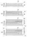
図2は、本発明の第1例の画像表示装置11(同図(d))の製造方法の要部を示す断面図である。この画像表示装置11では、表示側パネル21上に、保護部22が、樹脂硬化物層44によって貼付されている。<First example>
FIG. 2 is a cross-sectional view showing the main part of the manufacturing method of the image display device 11 (FIG. 2D) of the first example of the present invention. In the
画像表示装置11の製造工程を説明すると、樹脂硬化物層44で貼付する前の表示側パネル21は、図2(a)に示すように、板状のベース31上に、画像表示部を取り囲む枠体30を配置し、枠体30の内側のベース31上にバックライト32と該バックライト32よりも小さな液晶パネルから成る画像表示部33とをこの順序で配置した構成となっている。枠体30はベース31と一体であってもよい。 The manufacturing process of the
この状態では、画像表示部33と枠体30の間には最大幅数mmの隙間37が形成されており、隙間37の底面には、バックライト32の表面が露出している。 In this state, a
一方、図1(a)に示すように、保護部22は、光学ガラス又はアクリル樹脂等のプラスチックから成る透明板41の表面の縁付近に、黒色不透明の遮光膜42が印刷により形成されたものとなっている。遮光膜42は、外光反射を防止して画像表示装置11の見やすさを高めるため、またバックライト32の光が周囲に漏れないようにするために設けられている。なお、保護部22としては、シート状又はフィルム状の部材を使用してもよい。 On the other hand, as shown in FIG. 1 (a), the
第1例の画像表示装置11の製造方法では、まず、上述の状態の表示側パネル21の画像表示部33と枠体30に亘るように、隙間37の上から高粘度の光硬化型樹脂組成物34を塗布する。ここで、光硬化型樹脂組成物34の粘度は、隙間37内に浸入しない程度の高粘性とし、具体的には、25℃でコーンプレート型回転粘度計(コーンプレートのテーパ角度C35/2°、10rpm)で3000mPa・s以上とし、12000mPa・s以下とする。 In the manufacturing method of the
これにより、図2(b)に示すように、表示側パネル21上に、空隙37を残したまま光硬化型樹脂組成物層34を形成することができる。 Thereby, as shown in FIG. 2B, the photocurable
また、光硬化型樹脂組成物34の塗布量は、光硬化型樹脂組成物層34を硬化させた樹脂硬化物層44の厚みが50〜200μmとなるようにすることが好ましい。 Moreover, it is preferable that the application quantity of the
次に、保護部22の遮光膜42側の面を表示側パネル21に向け、透明板41を光硬化型樹脂組成物層34の表面に接触させ、透明板41と光硬化型樹脂組成物層34の間に気泡が混入しないように押圧し、図2(c)に示すように、透明板41と光硬化型樹脂樹脂組成物層34を密着させる。 Next, the surface of the
その後、保護部22上で紫外線ランプを点灯し、透明板41を通して紫外線を硬化型樹脂組成物層34に照射することにより、それを硬化させ、図2(d)に示すように、樹脂硬化物層44を形成する。こうして、保護部22と表示側パネル21とが樹脂硬化物層44で接着された画像表示装置11を得る。 Thereafter, an ultraviolet lamp is turned on on the
なお、遮光膜42の幅が広く、保護部22上のランプの紫外線が、遮光膜42と表示側パネル21の間の光硬化型樹脂組成物層34に十分に到達しない場合には、表示側パネル21及び保護部22の側方から紫外線を照射してもよい。 When the width of the
得られた画像表示装置11では、保護部22側から画像表示部11を見ると、バックライトパネル32による照明光により、画像表示部33に形成される文字、図形等が観察される。 In the obtained
この第1例では、光硬化型樹脂組成物層34を表示側パネル21上に形成したが、光硬化型樹脂組成物34を保護部22の遮光膜42側の面に塗布することにより、図1(b)に示すように、保護部22上に光硬化型樹脂組成物層34を形成しておき、それを図2(a)に示した表示側パネル21と重ね合わせ、上述と同様に紫外線を照射し、図2(d)に示す画像表示装置11を形成してもよい。 In this first example, the photocurable
<第2例>
図4は、第2例の画像表示装置12の製造方法の要部を示す断面図である。<Second example>
FIG. 4 is a cross-sectional view showing the main part of the method of manufacturing the
この第2例の製造方法では、光硬化型樹脂組成物として粘度が低く(3000mPa・s未満)、第1例のように表示側パネル21上に光硬化型樹脂組成物を塗布した場合には、図3に示すように、光硬化型樹脂組成物134が隙間37内に流入する樹脂組成物を使用する。図3に示すように、光硬化型樹脂組成物134が隙間37内に流入すると、その光硬化型樹脂組成物134は、バックライト32と画像表示部33の間に浸透し、表示不良が発生するおそれがある。 In the manufacturing method of the second example, when the photocurable resin composition has a low viscosity (less than 3000 mPa · s) and the photocurable resin composition is applied on the
そこで、第2例では、表示側パネル21上に光硬化型樹脂組成物を塗布する前に、図2(a)の状態の表示側パネル21の隙間37上に、図4(a)に示すように、画像表示部33と枠体30に亘って、接着性を有する密閉フィルム51を配置し、隙間37を閉塞する。密閉フィルム51の幅方向の一端は画像表示部33に密着し、他端は枠体30に密着するので、隙間37が密閉される。 Therefore, in the second example, before applying the photocurable resin composition on the
このような密閉フィルム51としては、ポリエチレンテレフタレート等をフィルム基材とし、アクリレート系等の粘着剤層あるいは接着層を有する粘着フィルムが好ましい。 As such a
なお、密閉フィルム51は、表示側パネル21への配置時に必ずしも粘着剤層あるいは接着剤層は固体である必要はなく、隙間37に入り込んだり、画像表示部33とバックライト32との間に浸入しない程度に高粘度であればよい。より具体的には粘度65000mPa・s程度の硬化型樹脂組成物を使用することができる。また、隙間37に入り込まない程度に基材フィルム上で形状を保持させる点から、チキソ比3程度の接着剤を使用してもよい。 The sealing
次に、図4(b)に示すように、画像表示部33と密閉フィルム51と枠体30に掛かるように表示側パネル21上に光硬化型樹脂組成物35を塗布する。そして、前述と同様に、図1(a)の保護部を、図4(c)に示すように、表示側パネル21上に重ね合わせ、その状態で、光硬化型樹脂組成物層35に紫外線を照射し、硬化させて図4(d)に示すように、樹脂硬化物層45を形成する。こうして、隙間37が密閉フィルム51で密閉された状態で、表示側パネル21と保護部22とが樹脂硬化物層45で接着されている第2例の画像表示装置12が得られる。 Next, as shown in FIG. 4B, a
この例でも、光硬化型樹脂組成物層35を保護部22に形成し、図4(a)の状態の表示側パネル21と図4(c)に示すように密着させ、光を照射して、図4(d)の画像表示装置12を得ることができる。 Also in this example, the photocurable
<第3例>
図5は、第3例の画像表示装置13の製造方法の要部を示す断面図である。<Third example>
FIG. 5 is a cross-sectional view showing the main part of the manufacturing method of the
この第3例の製造方法では、上記の第2例に対して、図5(a)に示すように、側縁部に突部62が周設された枠体61を有する表示側パネル24を使用する点が異なっている。 In the manufacturing method of the third example, as shown in FIG. 5A, the
この表示側パネル24でも、枠体61と画像表示部33の間には、底面にバックライト32が露出する隙間57が形成されている。 In the
そこで、先ず、同図(b)に示すように、隙間57上に、画像表示部33と枠体61に亘って密閉フィルム51を貼付し、隙間57を密閉する。 Therefore, first, as shown in FIG. 5B, the sealing
次いで、同図(c)に示すように、画像表示部33と密閉フィルム51と枠体61に掛かるように表示側パネル24上に光硬化型樹脂組成物36を滴下し、それを画像表示部33上に広げ光硬化型樹脂組成物層36を形成する。その後、同図(d)に示すように、前述と同様の保護部22を光硬化型樹脂組成物層36上に重ね合わせる。ここで、この表示側パネル24では枠体61に突部62が周設されているため、光硬化型樹脂組成物36を表示側パネル24上に滴下しても、その光硬化型樹脂組成物36が枠体61の周囲に流れ出さないという効果がある。このため、第3例では、光硬化型樹脂組成物36として、第2例よりもさらに低粘度のものを使用することができ、光硬化型樹脂組成物36の粘度に関する自由度が高くなる。 Next, as shown in FIG. 3C, a
保護部22を光硬化型樹脂組成物層36上に重ね合わせた後は、紫外線を照射して光硬化型樹脂組成物層36を硬化させ、同図(e)に示すように、樹脂硬化物層46とする。こうして、保護部22と表示側パネル24とが樹脂硬化物層46によって密着された第3例の画像表示装置13が得られる。 After the
なお、この第3例でも、光硬化型樹脂組成物層36を保護部22に形成し、図5(b)の状態の表示側パネル21と図5(d)に示すように密着させ、光照射して、図5(e)の画像表示装置13を得ることができる。 In this third example as well, the photocurable
以上の第1例〜第3例のいずれにおいても、光硬化型樹脂組成物34〜36としては、その樹脂硬化物の貯蔵弾性率(25℃)を好ましくは1×10⁷Pa以下、より好ましくは1×10³〜1×10⁶Paとし、樹脂硬化物の屈折率を好ましくは1.45以上1.55以下、より好ましくは1.51以上1.52以下とし、さらに、樹脂硬化物の厚さが100μmの場合の可視光領域の透過率を好ましくは90%以上とするように調製したものを用いる。In any of the above first to third examples, the
一般に、硬化型樹脂組成物を構成する主要な樹脂成分としては共通でも、共に配合する樹脂成分あるいはモノマー成分等が異なると、それを硬化させた樹脂硬化物の貯蔵弾性率(25℃)が1×10⁷Paを超える場合があるが、そのような樹脂硬化物となる樹脂組成物は、光硬化型樹脂組成物としては好ましくない。In general, even if the main resin component constituting the curable resin composition is common, if the resin component or monomer component blended together is different, the storage elastic modulus (25 ° C.) of the cured resin obtained by curing the resin component is 1 Although it may exceed 107 Pa, a resin composition that becomes such a cured resin is not preferable as a photocurable resin composition.
貯蔵弾性率が上述の範囲を超えると、表示色ムラが発生する場合がある。 If the storage elastic modulus exceeds the above range, display color unevenness may occur.
また、この光硬化型樹脂組成物34〜36は、硬化収縮率が、好ましくは5.0%以下、より好ましくは4.5%以下、特に好ましくは4.0%以下、さらに好ましくは0〜2%となるように調製したものとする。これにより、光硬化型樹脂組成物34〜36が硬化する際に樹脂硬化物に蓄積される内部応力を低減させることができ、樹脂硬化物層44、45、46と表示側パネル21、24又は保護部22との界面に歪みができることを防止できる。したがって、光硬化型樹脂組成物34〜36を表示パネル21、24と保護部22との間に介在させ、光硬化型樹脂組成物34〜36、134を硬化させた場合に、樹脂硬化物層44、45、46と表示側パネル22、24又は保護部22との界面で生じる光の散乱を低減させることができ、表示画像の輝度を高めると共に、視認性を向上させることができる。 In addition, the
これに対し、硬化収縮率が上述の範囲外であると、表示色ムラが発生する場合がある。 On the other hand, when the curing shrinkage rate is out of the above range, display color unevenness may occur.
なお、樹脂組成物が硬化する際に樹脂硬化物に蓄積される内部応力の程度は、樹脂組成物を平板上に滴下し、それを硬化させて得られる樹脂硬化物の平均表面粗度によって評価することができる。例えば、樹脂組成物2mgをガラス板上又はアクリル板上に滴下し、それをUV照射により90%以上の硬化率で硬化させて得られる樹脂硬化物の平均表面粗度が6.0nm以下であれば、表示側パネルと保護部との間に光硬化型樹脂組成物を介在させ、それを硬化させた場合にそれらの界面に生じる歪みが実用上無視できる。これに関し、本発明で好ましく使用する光硬化型樹脂組成物34〜36によれば、この平均表面粗度を6.0nm以下、好ましくは5.0nm以下、より好ましくは1〜3nmにすることができる。したがって、樹脂硬化物の界面に生じる歪みを実用上無視することができる。 The degree of internal stress accumulated in the cured resin when the resin composition is cured is evaluated by the average surface roughness of the cured resin obtained by dropping the resin composition on a flat plate and curing it. can do. For example, the average surface roughness of a cured resin obtained by dropping 2 mg of a resin composition on a glass plate or an acrylic plate and curing it with UV irradiation at a curing rate of 90% or more should be 6.0 nm or less. For example, when a photocurable resin composition is interposed between the display side panel and the protective part and cured, the distortion generated at the interface between them can be ignored in practice. In this regard, according to the
ここで、ガラス板としては、液晶セルの液晶を挟持するガラス板や液晶セルの保護板として使用されているものを好ましく使用できる。また、アクリル板としては、液晶セルの保護板として使用されているものを好ましく使用できる。これらのガラス板やアクリル板の平均表面粗度は、通常、1.0nm以下である。 Here, as a glass plate, what is used as a glass plate which clamps the liquid crystal of a liquid crystal cell, or a protective plate of a liquid crystal cell can be used preferably. Moreover, as an acrylic board, what is used as a protective plate of a liquid crystal cell can be used preferably. The average surface roughness of these glass plates and acrylic plates is usually 1.0 nm or less.
このような光硬化型樹脂組成物としては、例えば、ポリウレタンアクリレート、ポリイソプレン系アクリレート又はそのエステル化物、テルペン系水素添加樹脂、ブタジエン重合体等の1種以上のポリマーと、イソボルニルアクリレート、ジシクロペンテニルオキシエチルメタクリレート、2−ヒドロキシブチルメタクリレート等の1種以上のアクリレート系モノマーと、1−ヒドロキシ−シクロヘキシル−フェニル−ケトン等の光重合開始剤とを含有する樹脂組成物を好適に用いることができる。 Examples of such a photocurable resin composition include one or more polymers such as polyurethane acrylate, polyisoprene acrylate or esterified product thereof, terpene hydrogenated resin, butadiene polymer, isobornyl acrylate, diester, and the like. It is preferable to use a resin composition containing one or more acrylate monomers such as cyclopentenyloxyethyl methacrylate and 2-hydroxybutyl methacrylate and a photopolymerization initiator such as 1-hydroxy-cyclohexyl-phenyl-ketone. it can.
また、光硬化型樹脂組成物には、その他の添加剤、例えば増感剤、可塑剤、透明粒子等を本発明の目的の範囲で添加することができる。 In addition, other additives such as a sensitizer, a plasticizer, and transparent particles can be added to the photocurable resin composition within the scope of the object of the present invention.
なお、保護部22の透明板41には、画像表示部33に対する紫外線保護の観点から紫外線領域をカットする機能が付与されていることが多い。そのため、光重合開始剤としては、可視光領域でも硬化できる光重合開始剤(例えば、商品名 SpeedCure TPO、日本シイベルヘグナー(株)製等)を用い、照射光として、可視光を用いることが好ましい。 The
本発明の画像表示装置は、携帯電話の他、携帯ゲーム機器、電子手帳、形態測定器等の電子機器の表示部分の他、有機ELパネル、プラズマディスプレイ等の種々のパネルディスプレイに適用することが可能である。 The image display device of the present invention can be applied to various panel displays such as an organic EL panel and a plasma display in addition to a display portion of an electronic device such as a portable game device, an electronic notebook, and a shape measuring instrument in addition to a mobile phone. Is possible.
<第1例に相当する実施例1>
(1)樹脂組成物1の調製
ポリウレタンアクリレート(商品名 UV-3000B、日本合成化学工業(株)製)70重量部、イソボルニルアクリレート(商品名 IBXA、大阪有機化学工業(株)製)20重量部、光重合開始剤(商品名 イルガキュア184、チバ・スペシャリティ・ケミカルズ(株)製)4重量部、光重合開始剤(商品名 SpeedCure TPO、日本シイベルヘグナー(株)製)1重量部を、ガラス容器に投入して撹拌し、目的の光硬化型樹脂組成物を得た。<Example 1 corresponding to the first example>
(1) Preparation of Resin Composition 1 Polyurethane acrylate (trade name: UV-3000B, manufactured by Nippon Synthetic Chemical Industry Co., Ltd.) 70 parts by weight, isobornyl acrylate (trade name: IBXA, manufactured by Osaka Organic Chemical Industry Co., Ltd.) 20 1 part by weight of glass, 4 parts by weight of photopolymerization initiator (trade name: Irgacure 184, manufactured by Ciba Specialty Chemicals Co., Ltd.), 1 part by weight of photopolymerization initiator (trade name: SpeedCure TPO, manufactured by Nippon Shibel Hegner) The mixture was put into a container and stirred to obtain the desired photocurable resin composition.
(2)樹脂組成物1の評価
(2-1)粘度
(1)で得た樹脂組成物1の粘度(25℃)をコーンプレート型回転粘度計(HAAKE社製)、コーンプレートのテーパ角度C35/2°、10rpm)で測定したところ、10000mPa・sであった。(2) Evaluation of resin composition 1
(2-1) Viscosity The viscosity (25 ° C.) of the resin composition 1 obtained in (1) was measured with a cone plate type rotational viscometer (manufactured by HAAKE), cone plate taper angle C35 / 2 °, 10 rpm). However, it was 10,000 mPa · s.
(2-2)光透過率
(1)で得た樹脂組成物1を、厚さ100μmの白色のガラス板上に、所定の膜厚となるように滴下してUVコンベアにて搬送し、樹脂硬化物を得た。
こうして得た樹脂硬化物(厚さ100μm)について、紫外可視分光光度計(日本分光(株)製 V-560)を用いて可視光領域の透過率を測定した。その結果、樹脂硬化物の透過率は95%以上であった。(2-2) Light transmittance The resin composition 1 obtained in (1) is dropped onto a white glass plate having a thickness of 100 μm so as to have a predetermined film thickness, and is transported by a UV conveyor, and resin A cured product was obtained.
About the resin cured product thus obtained (thickness: 100 μm), the transmittance in the visible light region was measured using an ultraviolet-visible spectrophotometer (V-560 manufactured by JASCO Corporation). As a result, the transmittance of the cured resin was 95% or more.
(2-3)貯蔵弾性率
(2-2)と同様にして得た樹脂硬化物について、粘弾性測定装置(セイコーインスツルメンツ(株)製 DMS6100)を用い、測定周波数1Hzで貯蔵弾性率(Pa)(25℃)を測定したところ、1×10⁶Paであった。(2-3) Storage elastic modulus
The cured resin obtained in the same manner as in (2-2) was measured for storage elastic modulus (Pa) (25 ° C.) at a measurement frequency of 1 Hz using a viscoelasticity measuring device (DMS6100 manufactured by Seiko Instruments Inc.). 1 × 10⁶ Pa.
(2-4)硬化圧縮率
硬化前の樹脂液と硬化後の固体の比重を電子比重計(MIRAGE社製SD−120L)を用いて測定し、両者の比重差から次式により算出した。(2-4) Curing compressibility The specific gravity of the resin liquid before curing and the solid after curing was measured using an electronic hydrometer (SD-120L manufactured by MIRAGE), and calculated from the difference between the specific gravities by the following equation.

その結果、硬化収縮率は3.5%であった。 As a result, the cure shrinkage rate was 3.5%.
(2-5)表面粗度
(1)で得た樹脂組成物2mgを液晶セル用ガラス板に滴下し、UV硬化の際に生ずる内部応力により発生するガラス板表面の所定領域(2.93mm×2.20mm)の歪み(Ra:平均表面粗度)を、Zygo社製3次元非接触表面粗度測定計にて測定した。
その結果、表面粗度Raは、4.5nmであった。(2-5) Surface Roughness 2 mg of the resin composition obtained in (1) is dropped on a glass plate for a liquid crystal cell, and a predetermined region (2.93 mm × X) generated by internal stress generated during UV curing. 2.20 mm) strain (Ra: average surface roughness) was measured with a Zygo 3D non-contact surface roughness meter.
As a result, the surface roughness Ra was 4.5 nm.
(3)表示側パネルと保護部の貼り合わせ試験
図2の製造方法にしたがい、遮光膜42を有する保護部22に(1)で得た樹脂組成物1を滴下して保護部全体に硬化型樹脂組成物層を形成するとともに、該保護部22を反転させて、図2(a)で示す表示側パネル21の画像表示部33である液晶セルに密着するように配置した。液晶セルと枠体30の間には、0.5mmの隙間37があり、その底部にはバックライト32が露出しているが、樹脂組成物1は、隙間37にしみ込まなかった。(3) Bonding test of display side panel and protective part According to the manufacturing method of FIG. 2, the resin composition 1 obtained in (1) is dropped onto the
次いで、紫外線を照射することにより、樹脂組成物1を紫外線硬化させて樹脂硬化物層44とし、画像表示装置11を完成させた。 Subsequently, the resin composition 1 was cured with ultraviolet rays by irradiating with ultraviolet rays to form a cured
<比較例1>
実施例1と同様に、ポリウレタンアクリレート(商品名 UV−3000B、日本合成化学工業(株)製、イソボルニルアクリレート(商品名 IBXA、大阪有機化学工業(株)製)、光重合開始剤(商品名 イルガキュア184、チバ・スペシャリティ・ケミカルズ(株)製)、および光重合開始剤(商品名 SpeedCure TPO、日本シイベルヘグナー(株)製)を使用するとともに、その配合量のみ相違させた樹脂組成物2を調製し、実施例1と同様に、粘度、透過率、硬化圧縮率、表面粗度を測定し、貼り合わせ試験を行った。これらの結果を表1、表2に示すとともに、実施例1と対比する。<Comparative Example 1>
Similarly to Example 1, polyurethane acrylate (trade name: UV-3000B, manufactured by Nippon Synthetic Chemical Industry Co., Ltd.), isobornyl acrylate (trade name: IBXA, manufactured by Osaka Organic Chemical Industry Co., Ltd.), photopolymerization initiator (commercial product) Name Irgacure 184, manufactured by Ciba Specialty Chemicals Co., Ltd.), and a photopolymerization initiator (trade name SpeedCure TPO, manufactured by Nippon Siebel Hegner Co., Ltd.), and the resin composition 2 in which only the blending amount thereof is different Then, the viscosity, transmittance, curing compression rate, and surface roughness were measured and the lamination test was conducted in the same manner as in Example 1. These results are shown in Tables 1 and 2, and Example 1 and Contrast.
表1および表2から明らかなように、粘度がm3000Pa・s以下であると、透過率等の特性に関わらず、樹脂組成物のしみ込みがあり、画像不良の可能性がある。 As is clear from Tables 1 and 2, when the viscosity is m3000 Pa · s or less, the resin composition may penetrate, regardless of properties such as transmittance, and image defects may occur.
<第2例に相当する実施例2>
(1)密閉フィルムの作製
基材フィルムである100μm厚ポリエチレンテレフタレートに、粘着剤としてアクリレート系樹脂の粘着剤を100μm厚塗布し、幅5mmに切断して目的の密閉フィルムを得た。<Example 2 corresponding to the second example>
(1) Production of sealed film A 100 μm thick polyethylene terephthalate as a base film was coated with a 100 μm thick adhesive of an acrylate resin as an adhesive, and cut to a width of 5 mm to obtain a desired sealed film.
(2)表示側パネルと保護部の貼り合わせ試験
図4の製造方法にしたがい、図4(a)の画像表示部33となる液晶セルと枠体30との間の隙間37(0.5mm)に、上述の(1)で作製した密閉フィルム51を、液晶セルと枠体30とを架設するように貼り付けた。(2) Bonding test between display-side panel and protective part According to the manufacturing method of FIG. 4, a gap 37 (0.5 mm) between the liquid crystal cell to be the
次に、遮光膜42を有する保護部22に前述の樹脂組成物2を滴下して保護部全体に光硬化型樹脂組成物層を形成するとともに、該保護部22を反転させて、表示側パネル21の画像表示部33である液晶セルに密着するように配置した。液晶セルと枠体30の間には、0.5mmの隙間37があり、その底部にはバックライト32が露出しているが、樹脂組成物2は、密閉フィルム51の作用により隙間37には入り込まなかった。次いで、紫外線を照射することにより、樹脂樹脂組成物2を紫外線硬化させて樹脂硬化物層45を形成し、画像表示装置12を完成させた。 Next, the above resin composition 2 is dropped on the
上記の通り、第2例に相当する実施例2によれば、樹脂組成物の粘度が3000mPa・s以下であっても密閉フィルム51の作用により、隙間37へのしみ込みを防止することができる。 As described above, according to Example 2 corresponding to the second example, even if the viscosity of the resin composition is 3000 mPa · s or less, the sealing
<第2例に相当する実施例3>
(1)密閉フィルムの作製
剥離処理がされた100μm厚ポリエチレンテレフタレートに、粘着剤として実施例1の樹脂組成物1を50μm厚塗布し、幅5mmに切断して目的の密閉フィルムを得た。なお、この時点で密閉フィルムは光硬化していない。<Example 3 corresponding to the second example>
(1) Production of Sealing Film 50 μm of the resin composition 1 of Example 1 was applied as a pressure-sensitive adhesive to 100 μm thick polyethylene terephthalate subjected to the peeling treatment, and cut to a width of 5 mm to obtain a target sealing film. At this time, the sealing film is not photocured.
(2)表示側パネルと保護部の貼り合わせ試験
図4の製造方法にしたがい、図4(a)の画像表示部33となる液晶セルと枠体30との間の隙間37(0.5mm)に、上述の実施例3(1)で作製した密閉フィルム51を、液晶セルと枠体33に架設するように貼り付けた後、剥離フィルムを剥がした。(2) Bonding test between display-side panel and protective part According to the manufacturing method of FIG. 4, a gap 37 (0.5 mm) between the liquid crystal cell to be the
次に、遮光膜42を有する保護部22に前述の樹脂組成物2を滴下して保護部全体に光硬化型樹脂組成物層を形成するとともに、当該保護部22を反転させて、表示側パネル21の画像表示部33である液晶セルに密着するように配置した。液晶セルと枠体30の間には、0.5mmの隙間37があり、その底部にはバックライト32が露出しているが、樹脂組成物2は、密閉フィルム51の作用により隙間37には入り込まなかった。次いで、紫外線を照射することにより、樹脂組成物2を紫外線硬化させて樹脂硬化物層45を形成し、画像表示装置12を完成させた。なお、この密閉フィルム51で粘着剤として塗布した樹脂組成物1は、樹脂硬化物層45の形成時の紫外線硬化で硬化した。 Next, the resin composition 2 described above is dropped on the
本発明は、液晶表示装置などの画像表示装置等に有用である。 The present invention is useful for an image display device such as a liquid crystal display device.
11〜13……画像表示装置
21、24……表示側パネル
22 ……保護部
30、61……枠体
31 ……ベース
32 ……バックライト
33 ……画像表示部
34〜36、134……光硬化型樹脂組成物又は光硬化型樹脂組成物層
37、57……隙間
41 ……透明板
42 ……遮光膜
44、45、46……樹脂硬化物層
51 ……密閉フィルム11-13 ……
Claims (13)
Translated fromJapanese画像表示部と枠体との間に形成された隙間を閉塞する密閉フィルムが画像表示部と枠体との間に亘って配置され、密閉フィルム上に樹脂硬化物層が設けられている画像表示装置。A display-side panel having an image display unit and a frame surrounding the image display unit; a protective unit disposed on the display-side panel; and a cured resin layer interposed between the display-side panel and the protective unit An image display device,
An image display in which a sealing film that closes a gap formed between the image display unit and the frame is disposed between the image display unit and the frame, and a cured resin layer is provided on the sealing film. apparatus.
画像表示部と枠体との間に形成されている隙間を密閉フィルムで閉塞し、その上に光硬化型樹脂組成物を配置する画像表示装置の製造方法。A photo-curable resin composition is interposed between the image display unit and the frame body between the display side panel having the image display unit and a frame body surrounding the image display unit, and the protection unit, and is photocured. A method of manufacturing an image display device including a step of forming a cured resin layer,
The manufacturing method of the image display apparatus which obstruct | occludes the clearance gap formed between the image display part and the frame with a sealing film, and arrange | positions a photocurable resin composition on it.
Priority Applications (1)
| Application Number | Priority Date | Filing Date | Title |
|---|---|---|---|
| JP2008100879AJP5401824B2 (en) | 2007-04-09 | 2008-04-08 | Image display device |
Applications Claiming Priority (7)
| Application Number | Priority Date | Filing Date | Title |
|---|---|---|---|
| JP2007102239 | 2007-04-09 | ||
| JP2007102239 | 2007-04-09 | ||
| JP2007186360 | 2007-07-17 | ||
| JP2007186360 | 2007-07-17 | ||
| JP2008005027 | 2008-01-11 | ||
| JP2008005027 | 2008-01-11 | ||
| JP2008100879AJP5401824B2 (en) | 2007-04-09 | 2008-04-08 | Image display device |
Related Child Applications (1)
| Application Number | Title | Priority Date | Filing Date |
|---|---|---|---|
| JP2013215621ADivisionJP2014056250A (en) | 2007-04-09 | 2013-10-16 | Photo-curable resin composition |
Publications (2)
| Publication Number | Publication Date |
|---|---|
| JP2009186956A JP2009186956A (en) | 2009-08-20 |
| JP5401824B2true JP5401824B2 (en) | 2014-01-29 |
Family
ID=39863953
Family Applications (6)
| Application Number | Title | Priority Date | Filing Date |
|---|---|---|---|
| JP2008100879AActiveJP5401824B2 (en) | 2007-04-09 | 2008-04-08 | Image display device |
| JP2013215621APendingJP2014056250A (en) | 2007-04-09 | 2013-10-16 | Photo-curable resin composition |
| JP2015161711APendingJP2016014885A (en) | 2007-04-09 | 2015-08-19 | Photocurable resin composition |
| JP2017121431AActiveJP6443500B2 (en) | 2007-04-09 | 2017-06-21 | Photocurable resin composition |
| JP2018223551APendingJP2019086783A (en) | 2007-04-09 | 2018-11-29 | Photocurable resin composition |
| JP2021118142AActiveJP7239852B2 (en) | 2007-04-09 | 2021-07-16 | Method for manufacturing image display device |
Family Applications After (5)
| Application Number | Title | Priority Date | Filing Date |
|---|---|---|---|
| JP2013215621APendingJP2014056250A (en) | 2007-04-09 | 2013-10-16 | Photo-curable resin composition |
| JP2015161711APendingJP2016014885A (en) | 2007-04-09 | 2015-08-19 | Photocurable resin composition |
| JP2017121431AActiveJP6443500B2 (en) | 2007-04-09 | 2017-06-21 | Photocurable resin composition |
| JP2018223551APendingJP2019086783A (en) | 2007-04-09 | 2018-11-29 | Photocurable resin composition |
| JP2021118142AActiveJP7239852B2 (en) | 2007-04-09 | 2021-07-16 | Method for manufacturing image display device |
Country Status (7)
| Country | Link |
|---|---|
| US (3) | US8821966B2 (en) |
| EP (1) | EP2144218B1 (en) |
| JP (6) | JP5401824B2 (en) |
| KR (5) | KR101517739B1 (en) |
| CN (3) | CN101681571B (en) |
| TW (1) | TWI396000B (en) |
| WO (1) | WO2008126856A1 (en) |
Families Citing this family (43)
| Publication number | Priority date | Publication date | Assignee | Title |
|---|---|---|---|---|
| EP2824653B1 (en) | 2006-07-14 | 2016-06-29 | Dexerials Corporation | Resin composition and display apparatus |
| JP5401824B2 (en) | 2007-04-09 | 2014-01-29 | デクセリアルズ株式会社 | Image display device |
| JP2009186957A (en)* | 2007-04-09 | 2009-08-20 | Sony Chemical & Information Device Corp | Resin composition and display device |
| CN101675461B (en) | 2007-04-09 | 2013-11-13 | 迪睿合电子材料有限公司 | Image display device |
| JP5470735B2 (en)* | 2007-04-10 | 2014-04-16 | デクセリアルズ株式会社 | Manufacturing method of image display device |
| CN102253514B (en) | 2007-07-17 | 2014-11-26 | 迪睿合电子材料有限公司 | Image display device and method for manufacturing the same |
| WO2010044291A1 (en)* | 2008-10-17 | 2010-04-22 | シャープ株式会社 | Display device and method for manufacturing the same |
| JP2010107935A (en) | 2008-10-28 | 2010-05-13 | Samsung Mobile Display Co Ltd | Flat panel display device and method of fabricating the same |
| CN102985960B (en) | 2010-06-21 | 2015-04-29 | 夏普株式会社 | Display panel equipped with front plate, display device, and resin composition |
| KR101211371B1 (en) | 2010-09-16 | 2012-12-13 | 주식회사 토비스 | Method for manufacturing display panel with curved shape |
| JP5646262B2 (en)* | 2010-09-24 | 2014-12-24 | 三洋電機株式会社 | Image display device |
| EP2642469A1 (en) | 2010-11-17 | 2013-09-25 | Asahi Glass Company, Limited | Transparent protective plate, flat panel display, and method for producing flat panel display |
| JP5685270B2 (en) | 2011-01-18 | 2015-03-18 | シャープ株式会社 | Display panel with flat plate and method for manufacturing display panel with flat plate |
| JP2012172064A (en) | 2011-02-22 | 2012-09-10 | Nitto Denko Corp | Ultraviolet-curable optical resin adhesive composition |
| JP5651526B2 (en)* | 2011-04-28 | 2015-01-14 | 藤森工業株式会社 | Hard coat film and touch panel using the same |
| TWI627068B (en)* | 2011-10-14 | 2018-06-21 | Nitto Denko Corp | Unit for image display device with adhesive layer and image display device using the unit |
| MY170060A (en) | 2011-10-21 | 2019-07-02 | Nippon Kayaku Kk | Method for producing optical member and use of ultraviolet ray cured resin composition for same |
| KR20210090286A (en)* | 2012-01-25 | 2021-07-19 | 데쿠세리아루즈 가부시키가이샤 | Method of manufacturing image display device |
| TWI557204B (en) | 2012-02-17 | 2016-11-11 | Three Bond Fine Chemical Co Ltd | Optically hardened sheet-like adhesive composition |
| JP6018397B2 (en)* | 2012-04-09 | 2016-11-02 | 共同技研化学株式会社 | Double-sided pressure-sensitive adhesive sheet for information display surface, protective sheet for information display surface, and method for producing the double-sided pressure-sensitive adhesive sheet and protective sheet |
| KR101962550B1 (en) | 2012-05-09 | 2019-03-26 | 데쿠세리아루즈 가부시키가이샤 | Image display device manufacturing method |
| US9851593B2 (en)* | 2012-09-11 | 2017-12-26 | Apple Inc. | LCD frame assembly |
| KR20140052732A (en)* | 2012-10-25 | 2014-05-07 | 삼성디스플레이 주식회사 | Display device and method for manufacturing the same |
| HUE056672T2 (en) | 2012-12-14 | 2022-02-28 | Dexerials Corp | A method of making an image display device |
| JP5370706B1 (en)* | 2012-12-14 | 2013-12-18 | デクセリアルズ株式会社 | Manufacturing method of image display device |
| JP5994618B2 (en)* | 2012-12-14 | 2016-09-21 | デクセリアルズ株式会社 | Photocurable resin composition and method for producing image display device using the same |
| JP6011316B2 (en)* | 2012-12-21 | 2016-10-19 | 旭硝子株式会社 | Method for producing transparent face material with adhesive layer |
| EP2952528B1 (en)* | 2013-02-04 | 2017-11-15 | Bridgestone Corporation | Photocurable elastomer composition, gasket for hard disk drive, and hard disk drive |
| JP2014213572A (en)* | 2013-04-26 | 2014-11-17 | スリーエム イノベイティブプロパティズカンパニー | Method for producing laminate including cured pressure sensitive adhesive sheet |
| JP6609093B2 (en) | 2013-05-13 | 2019-11-20 | 日東電工株式会社 | Hard coat film, polarizing plate and image display device |
| DE102013226547B4 (en)* | 2013-12-18 | 2015-10-01 | Continental Automotive Gmbh | Method for producing a display unit and display unit |
| JP2015125182A (en)* | 2013-12-25 | 2015-07-06 | ソニー株式会社 | Display device |
| JP2017134091A (en)* | 2014-06-10 | 2017-08-03 | 旭硝子株式会社 | Transparent substrate with display device and table |
| EP3188163B1 (en)* | 2014-08-28 | 2022-04-06 | Sony Group Corporation | Display device |
| KR102435111B1 (en) | 2014-10-27 | 2022-08-22 | 씨테크 어드히시브스 엘엘씨 | Assembly processes using uv curable pressure sensitive adhesives (psa) or stageable psa systems |
| JP6622465B2 (en)* | 2015-02-17 | 2019-12-18 | 積水化学工業株式会社 | Light moisture curable resin composition cured body for narrow frame design display element |
| JP2017101779A (en)* | 2015-12-03 | 2017-06-08 | 株式会社コスモマテリアル | Protection method for gas piping facility |
| US9946104B2 (en) | 2015-12-28 | 2018-04-17 | Japan Display Inc. | Display device and method of manufacturing the same |
| CN109071328A (en)* | 2016-05-09 | 2018-12-21 | 日立化成株式会社 | Photocurable resin composition, photo-curable coating and solidfied material |
| KR102648021B1 (en)* | 2016-09-23 | 2024-03-15 | 삼성디스플레이 주식회사 | Display device and manufacturing the same |
| JP6393384B1 (en)* | 2017-10-06 | 2018-09-19 | 日本ペイント・オートモーティブコーティングス株式会社 | Method for forming antiglare hard coat layer |
| US12142621B2 (en)* | 2019-03-08 | 2024-11-12 | Dexerials Corporation | Method of manufacturing connection structure, connection structure, film structure, and method of manufacturing film structure |
| WO2023282117A1 (en) | 2021-07-05 | 2023-01-12 | 日油株式会社 | Di(meth)acrylate, photocurable resin composition, and photocurable resin composition for adhesive |
Family Cites Families (174)
| Publication number | Priority date | Publication date | Assignee | Title |
|---|---|---|---|---|
| JPH079562B2 (en) | 1983-10-07 | 1995-02-01 | カシオ計算機株式会社 | Mounting method of film type liquid crystal display cell |
| JPH01300246A (en) | 1988-05-28 | 1989-12-04 | Nippon Paint Co Ltd | Photosensitive resin composition for flexography |
| JPH02165188A (en) | 1988-12-19 | 1990-06-26 | Mitsubishi Electric Corp | display element |
| JPH03204616A (en) | 1990-01-08 | 1991-09-06 | Hitachi Ltd | lcd display |
| JPH0675701A (en) | 1992-08-25 | 1994-03-18 | Nitto Denko Corp | Production of liquid crystal display device |
| JPH0688963A (en)* | 1992-09-08 | 1994-03-29 | Rohm Co Ltd | Liquid crystal display panel |
| JPH06299126A (en) | 1993-02-19 | 1994-10-25 | Sekisui Chem Co Ltd | Heat-sensitive adhesive foam, its production, its composite material and its processing |
| JP3321718B2 (en) | 1993-04-01 | 2002-09-09 | 鈴木総業株式会社 | Method for manufacturing structure for preventing light scattering in liquid crystal display device |
| JPH0713173A (en) | 1993-06-22 | 1995-01-17 | Three Bond Co Ltd | Sealing agent for liquid crystal |
| JP3287661B2 (en) | 1993-08-30 | 2002-06-04 | 新日本製鐵株式会社 | Thermosetting resin composition, cured product thereof, and image forming material |
| JP3327423B2 (en) | 1993-10-21 | 2002-09-24 | 日本合成化学工業株式会社 | Manufacturing method of polarizing film |
| US5747152A (en) | 1993-12-02 | 1998-05-05 | Dai Nippon Printing Co., Ltd. | Transparent functional membrane containing functional ultrafine particles, transparent functional film, and process for producing the same |
| US5557436A (en)* | 1994-05-12 | 1996-09-17 | Magnascreen Corporation | Thin seal liquid crystal display and method of making same |
| JPH08122759A (en) | 1994-10-28 | 1996-05-17 | Sony Corp | Image display panel and production thereof |
| JP3083715B2 (en) | 1994-12-05 | 2000-09-04 | シャープ株式会社 | Manufacturing method of liquid crystal display element |
| JPH08211353A (en) | 1995-02-01 | 1996-08-20 | Nippondenso Co Ltd | Image display device |
| JP3230038B2 (en) | 1995-02-13 | 2001-11-19 | キヤノン株式会社 | Liquid crystal display |
| JP3331277B2 (en) | 1995-05-30 | 2002-10-07 | シャープ株式会社 | Manufacturing method of liquid crystal display device and liquid crystal display device |
| JP3272921B2 (en) | 1995-09-27 | 2002-04-08 | リンテック株式会社 | Adhesive sheet |
| US6204896B1 (en) | 1996-02-09 | 2001-03-20 | Seiko Instruments Inc. | Display unit, manufacturing method thereof and electronic device equipped with same |
| JP3220403B2 (en)* | 1996-02-09 | 2001-10-22 | セイコーインスツルメンツ株式会社 | Display device manufacturing method |
| JPH09318932A (en) | 1996-05-27 | 1997-12-12 | Nitto Denko Corp | Liquid crystal display |
| JP4013085B2 (en) | 1996-09-03 | 2007-11-28 | 東洋紡績株式会社 | Method for producing laminated film |
| JP3842347B2 (en) | 1996-09-09 | 2006-11-08 | セイコーインスツル株式会社 | Display device |
| JPH1095967A (en) | 1996-09-24 | 1998-04-14 | Olympus Optical Co Ltd | Adhesive composition and adhesion structure |
| JP3532051B2 (en)* | 1996-12-13 | 2004-05-31 | シャープ株式会社 | Liquid crystal panel fixing method and fixing device |
| JPH10293314A (en) | 1997-04-22 | 1998-11-04 | Toshiba Corp | Display device manufacturing method and manufacturing device |
| JP3799829B2 (en) | 1997-09-11 | 2006-07-19 | セイコーエプソン株式会社 | Electro-optical device, manufacturing method thereof, and projection display device |
| JP3499419B2 (en)* | 1997-11-11 | 2004-02-23 | 河口湖精密株式会社 | Liquid crystal display |
| JP2000007717A (en)* | 1998-06-19 | 2000-01-11 | Takeda Chem Ind Ltd | UV curable resin composition |
| JP2000073025A (en) | 1998-08-26 | 2000-03-07 | Sony Chem Corp | Tacky tape and its production |
| JP2000143756A (en)* | 1998-09-03 | 2000-05-26 | Nitto Denko Corp | Aromatic polycarbodiimide and its sheet |
| JP2000111908A (en) | 1998-10-05 | 2000-04-21 | Seiko Instruments Inc | Liquid crystal device |
| US6461709B1 (en) | 1998-10-28 | 2002-10-08 | 3M Innovative Properties Company | Graffiti and/or environmental protective article having removable sheets, substrates protected therewith, and a method of use |
| JP2000219868A (en) | 1998-11-16 | 2000-08-08 | Dainippon Ink & Chem Inc | Photocurable resin composition for liquid crystal panel seal |
| US6218446B1 (en)* | 1999-01-11 | 2001-04-17 | Dymax Corporation | Radiation curable formulation for producing electrically conductive resinous material, method of use, and article produced |
| JP2000258780A (en) | 1999-03-05 | 2000-09-22 | Mitsubishi Electric Corp | Liquid crystal display device and its production |
| US6414781B1 (en)* | 1999-03-30 | 2002-07-02 | Seiko Epson Corporation | Electro-optical device and projection display device including the same |
| JP3881962B2 (en)* | 1999-03-30 | 2007-02-14 | セイコーエプソン株式会社 | Electro-optical device and projection display device including the same |
| JP3697104B2 (en) | 1999-03-30 | 2005-09-21 | セイコーエプソン株式会社 | Liquid crystal device and projection display device having the same |
| EP1047055A1 (en) | 1999-04-22 | 2000-10-25 | 3M Innovative Properties Company | Optical storage medium |
| JP2001026758A (en) | 1999-04-28 | 2001-01-30 | Bridgestone Corp | Adhesive composition for optical function member integrated display device, adhesive film, adhesive film laminate, optical function member integrated display device, and method of manufacturing the same |
| DE60032131T2 (en) | 1999-05-10 | 2007-10-25 | Ciba Speciality Chemicals Holding Inc. | NEW PHOTOINITIATORS AND THEIR APPLICATIONS |
| JP4883433B2 (en) | 1999-05-16 | 2012-02-22 | 株式会社ワイエス・メディカル | Balloon catheter, method for manufacturing the same, and method for attaching balloon to catheter tube |
| JP2001222017A (en) | 1999-05-24 | 2001-08-17 | Fujitsu Ltd | Liquid crystal display device and method of manufacturing the same |
| KR100662534B1 (en)* | 1999-07-15 | 2006-12-28 | 가부시키가이샤 도모에가와 세이시쇼 | Method for forming single-layered powder coating film |
| JP2001290005A (en) | 1999-09-06 | 2001-10-19 | Seiko Epson Corp | cover glass |
| JP2001141907A (en) | 1999-11-12 | 2001-05-25 | Seiko Epson Corp | Microlens substrate manufacturing method, microlens substrate, counter substrate for liquid crystal panel, liquid crystal panel, and projection display device |
| JP2000267118A (en) | 2000-01-01 | 2000-09-29 | Matsushita Electric Ind Co Ltd | LCD panel |
| JP3560532B2 (en) | 2000-05-02 | 2004-09-02 | 株式会社巴川製紙所 | Antistatic film for display |
| WO2001087595A1 (en) | 2000-05-12 | 2001-11-22 | 3M Innovative Properties Company | Rigid substrate lamination process, system, and product |
| JP2002019013A (en) | 2000-07-05 | 2002-01-22 | Lintec Corp | Method for producing metal plate molding and adhesive sheet used in the method |
| JP2002040208A (en) | 2000-07-28 | 2002-02-06 | Nissha Printing Co Ltd | Antireflection cover component and method for producing the same |
| JP2002052552A (en) | 2000-08-11 | 2002-02-19 | Mitsubishi Chemicals Corp | Method of manufacturing photocurable resin sheet |
| JP2002092957A (en) | 2000-09-19 | 2002-03-29 | Mitsui Chemicals Inc | Material of surface protecting layer for optical recording medium |
| JP3607591B2 (en)* | 2000-10-04 | 2005-01-05 | Necアクセステクニカ株式会社 | Information terminal equipment |
| KR100387536B1 (en) | 2000-10-18 | 2003-06-18 | 주식회사 루밴틱스 | Optical Adhesive Composition for manufacturing optical adhesive filler and a method for manufacturing optical adhesive using the same |
| JP4118027B2 (en) | 2001-02-28 | 2008-07-16 | 株式会社日立製作所 | Liquid crystal display |
| EP1283106A4 (en) | 2001-03-15 | 2005-12-14 | Mitsui Chemicals Inc | Laminated body and display device using the laminated body |
| JP3733418B2 (en)* | 2001-04-16 | 2006-01-11 | シャープ株式会社 | Adhesive sheet, laminated sheet and liquid crystal display device |
| JP3710721B2 (en) | 2001-04-25 | 2005-10-26 | 三井化学株式会社 | Display filter manufacturing method |
| JP2002341776A (en) | 2001-05-16 | 2002-11-29 | Nitto Denko Corp | Film filter for preventing glass breakage and plasma display |
| JP2002341317A (en) | 2001-05-17 | 2002-11-27 | Sanyo Electric Co Ltd | Liquid crystal display device |
| JP5415658B2 (en) | 2001-05-28 | 2014-02-12 | 三菱樹脂株式会社 | Intermediate film adhesive sheet and transparent laminate |
| JP5045865B2 (en) | 2001-06-26 | 2012-10-10 | 株式会社ブリヂストン | Adhesive composition for optical functional member integrated display device and optical functional member integrated display device |
| JP2003029644A (en) | 2001-07-19 | 2003-01-31 | Mitsubishi Plastics Ind Ltd | Image display device, laminate for image display device, and transparent adhesive sheet used for panel of image display device |
| JP4755735B2 (en) | 2001-08-10 | 2011-08-24 | 三菱樹脂株式会社 | Base material for polarizing plate protective film |
| JP2003096425A (en) | 2001-09-21 | 2003-04-03 | Nippon Sheet Glass Co Ltd | Adhesive composition for fixing optical part |
| JP3860460B2 (en) | 2001-11-15 | 2006-12-20 | 三菱樹脂株式会社 | Filter-integrated image display device |
| JP4134559B2 (en) | 2002-01-15 | 2008-08-20 | 岩崎電気株式会社 | Hardener for sealing material of glass substrate for display panel |
| JP2003216059A (en)* | 2002-01-24 | 2003-07-30 | Sharp Corp | Indicating element and method of manufacturing the same |
| JP2003295780A (en) | 2002-03-29 | 2003-10-15 | Asahi Rubber:Kk | Electronic device image visibility improving structure, electronic device having the structure, and transparent member used in the structure |
| KR100813953B1 (en) | 2002-04-22 | 2008-03-14 | 삼성전자주식회사 | Photocurable resin composition having antistatic property |
| GB0212977D0 (en)* | 2002-06-06 | 2002-07-17 | Vantico Ag | Actinic radiation curable compositions and their use |
| JP4211295B2 (en) | 2002-06-11 | 2009-01-21 | 住友ベークライト株式会社 | Optical film sheet with barrier film and display element using the same |
| JP2004077887A (en) | 2002-06-18 | 2004-03-11 | Sony Corp | Display and electronic equipment having display |
| JP2004061925A (en) | 2002-07-30 | 2004-02-26 | Nippon Kayaku Co Ltd | Liquid crystal sealing agent and liquid crystal display cell using the same |
| JP2004117545A (en) | 2002-09-24 | 2004-04-15 | Mitsui Chemicals Inc | Method for manufacturing display filter |
| JP2004115757A (en) | 2002-09-30 | 2004-04-15 | Jsr Corp | Liquid curable resin composition |
| JP4047132B2 (en)* | 2002-10-21 | 2008-02-13 | キヤノン株式会社 | Manufacturing method of display element |
| JP4208187B2 (en) | 2002-10-28 | 2009-01-14 | 日東電工株式会社 | Adhesive optical film, method for producing adhesive optical film, and image display device |
| JP4251060B2 (en) | 2002-11-06 | 2009-04-08 | 住友化学株式会社 | Acrylic resin, pressure-sensitive adhesive containing the resin, and optical laminate formed by laminating the pressure-sensitive adhesive |
| JP2004212521A (en) | 2002-12-27 | 2004-07-29 | Mitsubishi Plastics Ind Ltd | Liquid crystal display |
| JP2004224855A (en) | 2003-01-21 | 2004-08-12 | Matsushita Electric Ind Co Ltd | Bonding method |
| JP4519409B2 (en) | 2003-02-24 | 2010-08-04 | リンテック株式会社 | Adhesive sheet and method of using the same |
| US7208206B2 (en) | 2003-03-10 | 2007-04-24 | Nitto Denko Corporation | Glass crack prevention laminate and liquid crystal display device |
| JP2004271935A (en) | 2003-03-10 | 2004-09-30 | Nitto Denko Corp | Optical film with adhesive and liquid crystal display |
| JP4232004B2 (en)* | 2003-03-11 | 2009-03-04 | 三菱樹脂株式会社 | Biaxially oriented polyester film |
| JP2004272059A (en)* | 2003-03-11 | 2004-09-30 | Ge Toshiba Silicones Co Ltd | Liquid crystal display device and portable electronic device having the same |
| JP2004279946A (en) | 2003-03-18 | 2004-10-07 | Sharp Corp | 2D / 3D switching type liquid crystal display panel and 2D / 3D switching type liquid crystal display device |
| JP2004325788A (en) | 2003-04-24 | 2004-11-18 | Sony Corp | Method and apparatus for optical inspection, and method for manufacturing liquid crystal display device |
| JP2004359769A (en) | 2003-06-03 | 2004-12-24 | Sekisui Chem Co Ltd | Photocurable adhesive composition for liquid-crystal panel, method for bonding liquid-crystal panel, method for sticking polarizing plate and liquid-crystal panel element |
| EP1634910A4 (en) | 2003-06-13 | 2006-07-26 | Jsr Corp | Transparent sheet and process for producing the same |
| JP4572590B2 (en) | 2003-06-13 | 2010-11-04 | Jsr株式会社 | Transparent sheet and method for producing the same |
| JP2005055641A (en) | 2003-08-04 | 2005-03-03 | Yokogawa Electric Corp | Liquid crystal display |
| JP4815768B2 (en) | 2003-08-22 | 2011-11-16 | 旭硝子株式会社 | Display device and manufacturing method of display device |
| US7382422B2 (en) | 2003-08-22 | 2008-06-03 | Asahi Glass Company, Limited | LCD with resin layer between front plate and substrate |
| JP4170861B2 (en) | 2003-09-04 | 2008-10-22 | 電気化学工業株式会社 | Photocurable resin composition |
| JP4275138B2 (en)* | 2003-09-11 | 2009-06-10 | 帝人デュポンフィルム株式会社 | Polyester film for reflector |
| US6842288B1 (en)* | 2003-10-30 | 2005-01-11 | 3M Innovative Properties Company | Multilayer optical adhesives and articles |
| JP4583749B2 (en) | 2003-11-26 | 2010-11-17 | 日東電工株式会社 | Pressure sensitive adhesive sheet |
| US20050126697A1 (en) | 2003-12-11 | 2005-06-16 | International Business Machines Corporation | Photochemically and thermally curable adhesive formulations |
| JP2005179481A (en)* | 2003-12-18 | 2005-07-07 | Nitto Denko Corp | Laminated sheet and liquid crystal display device |
| JP3798003B2 (en) | 2004-02-05 | 2006-07-19 | 沖電気工業株式会社 | Die bonding apparatus and die bonding method |
| JP4341424B2 (en)* | 2004-02-06 | 2009-10-07 | ソニー株式会社 | Display device |
| JP2005225127A (en) | 2004-02-13 | 2005-08-25 | Mitsubishi Chem Mkv Co | Laminated film |
| WO2005078524A1 (en)* | 2004-02-16 | 2005-08-25 | Mitsubishi Chemical Corporation | Curable resin composition, color filter and liquid crystal display |
| JP2005234129A (en) | 2004-02-18 | 2005-09-02 | Sekisui Chem Co Ltd | Hardening resin composition for liquid crystal display element, sealing material for liquid crystal display element, vertical conduction material, and liquid crystal display element |
| JP2005242099A (en) | 2004-02-27 | 2005-09-08 | Nec Lcd Technologies Ltd | Liquid crystal display |
| JP2005283749A (en) | 2004-03-29 | 2005-10-13 | Sony Corp | Optical diffusion film, its manufacturing method, and screen |
| JP2005315901A (en) | 2004-03-31 | 2005-11-10 | Optrex Corp | Display device |
| JP2005314687A (en) | 2004-03-31 | 2005-11-10 | Sekisui Chem Co Ltd | Photo-curable resin composition, cationic photopolymerization initiator, adhesive for display element and display element |
| US20050249683A1 (en)* | 2004-04-27 | 2005-11-10 | L Alloret Florence | Nail varnish composition comprising a polymer comprising units with a lower critical solution temperature |
| JP4370207B2 (en)* | 2004-06-29 | 2009-11-25 | シャープ株式会社 | Liquid crystal display |
| JP4527012B2 (en) | 2004-07-12 | 2010-08-18 | 日東電工株式会社 | Optical film with adhesive and image display device |
| JPWO2006011461A1 (en) | 2004-07-27 | 2008-07-31 | Jsr株式会社 | Shock absorber, shock absorbing laminated structure, shock absorbing laminated structure for liquid crystal display, shock absorbing laminated structure for plasma display, shock absorbing laminated structure for organic electroluminescent display and display device |
| JP2006053425A (en) | 2004-08-13 | 2006-02-23 | Dainippon Ink & Chem Inc | Photocurable composition for liquid crystal panel seal and liquid crystal panel |
| JP5207095B2 (en) | 2004-09-30 | 2013-06-12 | 大日本印刷株式会社 | Optical laminate |
| JP4527489B2 (en) | 2004-10-07 | 2010-08-18 | 大日本印刷株式会社 | Thermosetting resin composition for color filter, color filter, liquid crystal panel, and method for producing color filter |
| JP2006113435A (en) | 2004-10-18 | 2006-04-27 | Citizen Watch Co Ltd | Optical controller and liquid crystal display device |
| JP2006129678A (en) | 2004-11-01 | 2006-05-18 | Sony Corp | Power supply device |
| WO2006049296A1 (en) | 2004-11-08 | 2006-05-11 | Mitsubishi Chemical Corporation | Radiation curable composition and curing product thereof, and laminate including the same |
| JP2006137795A (en) | 2004-11-10 | 2006-06-01 | Mitsubishi Chemicals Corp | Radiation curable composition, cured product thereof, and laminate thereof |
| JP4609051B2 (en) | 2004-11-29 | 2011-01-12 | Jsr株式会社 | Shock absorbing laminated structure, LCD, plasma display, organic EL display, field emission display or shock absorbing laminated structure for electronic paper, and display device |
| JP2006159412A (en) | 2004-12-02 | 2006-06-22 | Nippon Paint Co Ltd | Composite film forming method and composite film |
| JP2006193730A (en) | 2004-12-15 | 2006-07-27 | Toray Ind Inc | Polyester film |
| JP2006189715A (en)* | 2005-01-07 | 2006-07-20 | Pentax Corp | Protective cover for display panel and its use |
| US8462301B2 (en)* | 2005-01-19 | 2013-06-11 | Stephen Derby O'Donnell | High-strength optical bonding method using optical silicone as a bonding medium and pressure sensitive adhesive as an intermediate layer |
| JP4515357B2 (en) | 2005-01-27 | 2010-07-28 | リンテック株式会社 | Adhesive for polarizing plate, polarizing plate with adhesive and method for producing the same |
| JP2006241234A (en) | 2005-03-01 | 2006-09-14 | Nippon Synthetic Chem Ind Co Ltd:The | Coating agent for optical recording medium and optical recording medium |
| KR101146964B1 (en) | 2005-03-18 | 2012-05-23 | 덴끼 가가꾸 고교 가부시키가이샤 | Adherent composition and method of temporarily fixing member therewith |
| JP2006267502A (en) | 2005-03-23 | 2006-10-05 | Fuji Xerox Co Ltd | Optical waveguide module |
| JP2006276105A (en)* | 2005-03-28 | 2006-10-12 | Toray Ind Inc | Manufacturing method of flat display member |
| JP2006277828A (en) | 2005-03-29 | 2006-10-12 | Tdk Corp | Optical recording medium |
| JP2006282911A (en) | 2005-04-01 | 2006-10-19 | Three M Innovative Properties Co | Pressure sensitive adhesive composition and adhesive tape |
| JP2006292993A (en) | 2005-04-11 | 2006-10-26 | Mitsubishi Electric Corp | Bonding device |
| TW200636032A (en) | 2005-04-13 | 2006-10-16 | Lg Chemical Ltd | Acrylic adhesive composition having excellent impact resistance, optical film using the adhesive composition, and liquid crystal display comprising the optical film |
| JP2006293239A (en) | 2005-04-14 | 2006-10-26 | Bridgestone Corp | Optical filter, and display and plasma display panel equipped with same |
| JP4801925B2 (en) | 2005-04-15 | 2011-10-26 | 株式会社ブリヂストン | Composition for photo-curing sealing material and member with sealing layer using the same |
| JP2006308866A (en) | 2005-04-28 | 2006-11-09 | Nippon Shinku Kagaku Kenkyusho:Kk | Polarization conversion element and liquid crystal display device using the same |
| WO2006121174A1 (en)* | 2005-05-10 | 2006-11-16 | Nippon Shokubai Co., Ltd. | Pressure-sensitive adhesive composition comprising near infrared ray absorption agent |
| US20090128767A1 (en) | 2005-05-30 | 2009-05-21 | Minoru Suezaki | Curable resin composition for column spacer,column spacer, and liquid crystal display panel |
| JP2006342222A (en)* | 2005-06-08 | 2006-12-21 | Mitsuyoshi Sato | Light-curable resin composition |
| JP2006349736A (en) | 2005-06-13 | 2006-12-28 | Dainippon Printing Co Ltd | Optical filter and manufacturing method thereof |
| JP2007004085A (en) | 2005-06-27 | 2007-01-11 | Asahi Glass Co Ltd | Light control device and manufacturing method thereof |
| JP2007010769A (en) | 2005-06-28 | 2007-01-18 | Nippon Kayaku Co Ltd | Liquid crystal sealing agent and liquid crystal display cell using same |
| JP5283146B2 (en)* | 2005-07-01 | 2013-09-04 | 株式会社ジャパンディスプレイ | Liquid crystal display |
| JP4743493B2 (en)* | 2005-07-01 | 2011-08-10 | 日立化成工業株式会社 | Shock absorbing resin composition for liquid crystal display, shock absorbing material for liquid crystal display using the same, optical filter for liquid crystal display using the same, and liquid crystal display |
| JP2007023147A (en)* | 2005-07-15 | 2007-02-01 | Toagosei Co Ltd | Active energy ray-curable composition for optical material |
| JP4924425B2 (en) | 2005-07-19 | 2012-04-25 | 東洋インキScホールディングス株式会社 | Curable composition, cured film and laminate |
| JP5011676B2 (en) | 2005-08-12 | 2012-08-29 | 株式会社日立製作所 | Equipment provided with display device |
| JP4459880B2 (en)* | 2005-09-15 | 2010-04-28 | 電気化学工業株式会社 | Energy ray curable resin composition and adhesive using the same |
| JP4483833B2 (en) | 2005-09-22 | 2010-06-16 | エプソンイメージングデバイス株式会社 | Electro-optical device, electronic apparatus, protective member, and manufacturing method of protective member |
| JP2007108592A (en) | 2005-10-17 | 2007-04-26 | Nitto Denko Corp | Laminated body for liquid crystal display device and liquid crystal display device including the same |
| JP2007140220A (en) | 2005-11-21 | 2007-06-07 | Hitachi Ltd | Display device |
| CN101317205B (en) | 2005-11-29 | 2010-11-03 | 精工电子有限公司 | Process for producing display and method of laminating |
| JP5098162B2 (en) | 2005-12-05 | 2012-12-12 | 日立化成工業株式会社 | Optical functional film for liquid crystal display with adhesive composition layer and liquid crystal display including the same |
| CN101331529B (en) | 2005-12-05 | 2011-03-30 | 精工电子有限公司 | Display device and method for manufacturing display device |
| JP2007163627A (en) | 2005-12-12 | 2007-06-28 | Epson Imaging Devices Corp | Illumination device, electro-optical device and electronic apparatus |
| JP2007186360A (en) | 2006-01-11 | 2007-07-26 | Taiheiyo Cement Corp | Cement composition |
| JP2007249038A (en) | 2006-03-17 | 2007-09-27 | Toppan Printing Co Ltd | Optical element, polarizing plate and liquid crystal display device using the same |
| JP2007298667A (en) | 2006-04-28 | 2007-11-15 | Hitachi Chem Co Ltd | Optical filter |
| JP2008005027A (en) | 2006-06-20 | 2008-01-10 | Morikawa Denki:Kk | Display stand |
| EP2824653B1 (en) | 2006-07-14 | 2016-06-29 | Dexerials Corporation | Resin composition and display apparatus |
| JP2007102251A (en) | 2007-01-22 | 2007-04-19 | Kyocera Mita Corp | Image forming apparatus and method for cleaning photoreceptor drum |
| JP4542553B2 (en) | 2007-01-22 | 2010-09-15 | 株式会社リコー | Image forming apparatus |
| CN101652803B (en) | 2007-04-03 | 2015-02-04 | 迪睿合电子材料有限公司 | Method for manufacturing image display device |
| WO2008123551A1 (en) | 2007-04-03 | 2008-10-16 | Sony Chemical & Information Device Corporation | Method for manufacturing image display |
| CN103399424B (en) | 2007-04-04 | 2017-04-26 | 迪睿合电子材料有限公司 | Method for manufacturing image display |
| JP2009186957A (en) | 2007-04-09 | 2009-08-20 | Sony Chemical & Information Device Corp | Resin composition and display device |
| JP5401824B2 (en) | 2007-04-09 | 2014-01-29 | デクセリアルズ株式会社 | Image display device |
| JP5571879B2 (en) | 2008-05-13 | 2014-08-13 | 株式会社豊田中央研究所 | Power transmission device |
| JP4623685B2 (en)* | 2009-03-26 | 2011-02-02 | 次世代モバイル用表示材料技術研究組合 | Manufacturing method of display device |
| JP5845679B2 (en)* | 2011-07-21 | 2016-01-20 | セイコーエプソン株式会社 | Electro-optical device, method of manufacturing electro-optical device, and projection display device |
- 2008
- 2008-04-08JPJP2008100879Apatent/JP5401824B2/enactiveActive
- 2008-04-09KRKR1020147003818Apatent/KR101517739B1/enactiveActive
- 2008-04-09CNCN2008800159275Apatent/CN101681571B/enactiveActive
- 2008-04-09CNCN201110129612.7Apatent/CN102176089B/enactiveActive
- 2008-04-09KRKR1020167017497Apatent/KR102056048B1/enactiveActive
- 2008-04-09KRKR1020197031754Apatent/KR102198385B1/enactiveActive
- 2008-04-09WOPCT/JP2008/056996patent/WO2008126856A1/enactiveApplication Filing
- 2008-04-09CNCN201310056745.5Apatent/CN103149726B/enactiveActive
- 2008-04-09KRKR1020157001682Apatent/KR20150017770A/ennot_activeCeased
- 2008-04-09USUS12/450,263patent/US8821966B2/enactiveActive
- 2008-04-09EPEP08740099.0Apatent/EP2144218B1/enactiveActive
- 2008-04-09TWTW097112940Apatent/TWI396000B/enactive
- 2008-04-09KRKR1020097021093Apatent/KR101419093B1/enactiveActive
- 2013
- 2013-10-16JPJP2013215621Apatent/JP2014056250A/enactivePending
- 2014
- 2014-06-09USUS14/299,902patent/US9348062B2/enactiveActive
- 2015
- 2015-08-19JPJP2015161711Apatent/JP2016014885A/enactivePending
- 2016
- 2016-01-04USUS14/987,012patent/US9354462B2/enactiveActive
- 2017
- 2017-06-21JPJP2017121431Apatent/JP6443500B2/enactiveActive
- 2018
- 2018-11-29JPJP2018223551Apatent/JP2019086783A/enactivePending
- 2021
- 2021-07-16JPJP2021118142Apatent/JP7239852B2/enactiveActive
Also Published As
Similar Documents
| Publication | Publication Date | Title |
|---|---|---|
| JP6443500B2 (en) | Photocurable resin composition | |
| JP5310913B2 (en) | Manufacturing method of image display device | |
| CN101681576B (en) | Method for manufacturing image display device, and image display device | |
| JP2009186954A (en) | Method of manufacturing image display apparatus | |
| HK1140302B (en) | Image display device | |
| HK1158763B (en) | An image display device | |
| HK1183108B (en) | An image display device |
Legal Events
| Date | Code | Title | Description |
|---|---|---|---|
| A621 | Written request for application examination | Free format text:JAPANESE INTERMEDIATE CODE: A621 Effective date:20101028 | |
| A977 | Report on retrieval | Free format text:JAPANESE INTERMEDIATE CODE: A971007 Effective date:20130430 | |
| A131 | Notification of reasons for refusal | Free format text:JAPANESE INTERMEDIATE CODE: A131 Effective date:20130507 | |
| A521 | Request for written amendment filed | Free format text:JAPANESE INTERMEDIATE CODE: A523 Effective date:20130703 | |
| TRDD | Decision of grant or rejection written | ||
| A01 | Written decision to grant a patent or to grant a registration (utility model) | Free format text:JAPANESE INTERMEDIATE CODE: A01 Effective date:20131001 | |
| A61 | First payment of annual fees (during grant procedure) | Free format text:JAPANESE INTERMEDIATE CODE: A61 Effective date:20131014 | |
| R150 | Certificate of patent or registration of utility model | Ref document number:5401824 Country of ref document:JP Free format text:JAPANESE INTERMEDIATE CODE: R150 | |
| R250 | Receipt of annual fees | Free format text:JAPANESE INTERMEDIATE CODE: R250 | |
| R250 | Receipt of annual fees | Free format text:JAPANESE INTERMEDIATE CODE: R250 | |
| R250 | Receipt of annual fees | Free format text:JAPANESE INTERMEDIATE CODE: R250 | |
| R250 | Receipt of annual fees | Free format text:JAPANESE INTERMEDIATE CODE: R250 | |
| R250 | Receipt of annual fees | Free format text:JAPANESE INTERMEDIATE CODE: R250 | |
| R250 | Receipt of annual fees | Free format text:JAPANESE INTERMEDIATE CODE: R250 | |
| R250 | Receipt of annual fees | Free format text:JAPANESE INTERMEDIATE CODE: R250 | |
| R250 | Receipt of annual fees | Free format text:JAPANESE INTERMEDIATE CODE: R250 | |
| R250 | Receipt of annual fees | Free format text:JAPANESE INTERMEDIATE CODE: R250 |