JP5386046B1 - Susceptor support and epitaxial growth apparatus provided with this susceptor support - Google Patents
Susceptor support and epitaxial growth apparatus provided with this susceptor supportDownload PDFInfo
- Publication number
- JP5386046B1 JP5386046B1JP2013066897AJP2013066897AJP5386046B1JP 5386046 B1JP5386046 B1JP 5386046B1JP 2013066897 AJP2013066897 AJP 2013066897AJP 2013066897 AJP2013066897 AJP 2013066897AJP 5386046 B1JP5386046 B1JP 5386046B1
- Authority
- JP
- Japan
- Prior art keywords
- susceptor
- arm
- arm portion
- support
- shaft
- Prior art date
- Legal status (The legal status is an assumption and is not a legal conclusion. Google has not performed a legal analysis and makes no representation as to the accuracy of the status listed.)
- Active
Links
Images


Classifications
- C—CHEMISTRY; METALLURGY
- C30—CRYSTAL GROWTH
- C30B—SINGLE-CRYSTAL GROWTH; UNIDIRECTIONAL SOLIDIFICATION OF EUTECTIC MATERIAL OR UNIDIRECTIONAL DEMIXING OF EUTECTOID MATERIAL; REFINING BY ZONE-MELTING OF MATERIAL; PRODUCTION OF A HOMOGENEOUS POLYCRYSTALLINE MATERIAL WITH DEFINED STRUCTURE; SINGLE CRYSTALS OR HOMOGENEOUS POLYCRYSTALLINE MATERIAL WITH DEFINED STRUCTURE; AFTER-TREATMENT OF SINGLE CRYSTALS OR A HOMOGENEOUS POLYCRYSTALLINE MATERIAL WITH DEFINED STRUCTURE; APPARATUS THEREFOR
- C30B25/00—Single-crystal growth by chemical reaction of reactive gases, e.g. chemical vapour-deposition growth
- C30B25/02—Epitaxial-layer growth
- C30B25/12—Substrate holders or susceptors
- C—CHEMISTRY; METALLURGY
- C23—COATING METALLIC MATERIAL; COATING MATERIAL WITH METALLIC MATERIAL; CHEMICAL SURFACE TREATMENT; DIFFUSION TREATMENT OF METALLIC MATERIAL; COATING BY VACUUM EVAPORATION, BY SPUTTERING, BY ION IMPLANTATION OR BY CHEMICAL VAPOUR DEPOSITION, IN GENERAL; INHIBITING CORROSION OF METALLIC MATERIAL OR INCRUSTATION IN GENERAL
- C23C—COATING METALLIC MATERIAL; COATING MATERIAL WITH METALLIC MATERIAL; SURFACE TREATMENT OF METALLIC MATERIAL BY DIFFUSION INTO THE SURFACE, BY CHEMICAL CONVERSION OR SUBSTITUTION; COATING BY VACUUM EVAPORATION, BY SPUTTERING, BY ION IMPLANTATION OR BY CHEMICAL VAPOUR DEPOSITION, IN GENERAL
- C23C16/00—Chemical coating by decomposition of gaseous compounds, without leaving reaction products of surface material in the coating, i.e. chemical vapour deposition [CVD] processes
- C23C16/44—Chemical coating by decomposition of gaseous compounds, without leaving reaction products of surface material in the coating, i.e. chemical vapour deposition [CVD] processes characterised by the method of coating
- C23C16/4412—Details relating to the exhausts, e.g. pumps, filters, scrubbers, particle traps
- C—CHEMISTRY; METALLURGY
- C23—COATING METALLIC MATERIAL; COATING MATERIAL WITH METALLIC MATERIAL; CHEMICAL SURFACE TREATMENT; DIFFUSION TREATMENT OF METALLIC MATERIAL; COATING BY VACUUM EVAPORATION, BY SPUTTERING, BY ION IMPLANTATION OR BY CHEMICAL VAPOUR DEPOSITION, IN GENERAL; INHIBITING CORROSION OF METALLIC MATERIAL OR INCRUSTATION IN GENERAL
- C23C—COATING METALLIC MATERIAL; COATING MATERIAL WITH METALLIC MATERIAL; SURFACE TREATMENT OF METALLIC MATERIAL BY DIFFUSION INTO THE SURFACE, BY CHEMICAL CONVERSION OR SUBSTITUTION; COATING BY VACUUM EVAPORATION, BY SPUTTERING, BY ION IMPLANTATION OR BY CHEMICAL VAPOUR DEPOSITION, IN GENERAL
- C23C16/00—Chemical coating by decomposition of gaseous compounds, without leaving reaction products of surface material in the coating, i.e. chemical vapour deposition [CVD] processes
- C23C16/44—Chemical coating by decomposition of gaseous compounds, without leaving reaction products of surface material in the coating, i.e. chemical vapour deposition [CVD] processes characterised by the method of coating
- C23C16/455—Chemical coating by decomposition of gaseous compounds, without leaving reaction products of surface material in the coating, i.e. chemical vapour deposition [CVD] processes characterised by the method of coating characterised by the method used for introducing gases into reaction chamber or for modifying gas flows in reaction chamber
- C23C16/45563—Gas nozzles
- C—CHEMISTRY; METALLURGY
- C23—COATING METALLIC MATERIAL; COATING MATERIAL WITH METALLIC MATERIAL; CHEMICAL SURFACE TREATMENT; DIFFUSION TREATMENT OF METALLIC MATERIAL; COATING BY VACUUM EVAPORATION, BY SPUTTERING, BY ION IMPLANTATION OR BY CHEMICAL VAPOUR DEPOSITION, IN GENERAL; INHIBITING CORROSION OF METALLIC MATERIAL OR INCRUSTATION IN GENERAL
- C23C—COATING METALLIC MATERIAL; COATING MATERIAL WITH METALLIC MATERIAL; SURFACE TREATMENT OF METALLIC MATERIAL BY DIFFUSION INTO THE SURFACE, BY CHEMICAL CONVERSION OR SUBSTITUTION; COATING BY VACUUM EVAPORATION, BY SPUTTERING, BY ION IMPLANTATION OR BY CHEMICAL VAPOUR DEPOSITION, IN GENERAL
- C23C16/00—Chemical coating by decomposition of gaseous compounds, without leaving reaction products of surface material in the coating, i.e. chemical vapour deposition [CVD] processes
- C23C16/44—Chemical coating by decomposition of gaseous compounds, without leaving reaction products of surface material in the coating, i.e. chemical vapour deposition [CVD] processes characterised by the method of coating
- C23C16/458—Chemical coating by decomposition of gaseous compounds, without leaving reaction products of surface material in the coating, i.e. chemical vapour deposition [CVD] processes characterised by the method of coating characterised by the method used for supporting substrates in the reaction chamber
- C23C16/4582—Rigid and flat substrates, e.g. plates or discs
- C23C16/4583—Rigid and flat substrates, e.g. plates or discs the substrate being supported substantially horizontally
- C23C16/4584—Rigid and flat substrates, e.g. plates or discs the substrate being supported substantially horizontally the substrate being rotated
- C—CHEMISTRY; METALLURGY
- C23—COATING METALLIC MATERIAL; COATING MATERIAL WITH METALLIC MATERIAL; CHEMICAL SURFACE TREATMENT; DIFFUSION TREATMENT OF METALLIC MATERIAL; COATING BY VACUUM EVAPORATION, BY SPUTTERING, BY ION IMPLANTATION OR BY CHEMICAL VAPOUR DEPOSITION, IN GENERAL; INHIBITING CORROSION OF METALLIC MATERIAL OR INCRUSTATION IN GENERAL
- C23C—COATING METALLIC MATERIAL; COATING MATERIAL WITH METALLIC MATERIAL; SURFACE TREATMENT OF METALLIC MATERIAL BY DIFFUSION INTO THE SURFACE, BY CHEMICAL CONVERSION OR SUBSTITUTION; COATING BY VACUUM EVAPORATION, BY SPUTTERING, BY ION IMPLANTATION OR BY CHEMICAL VAPOUR DEPOSITION, IN GENERAL
- C23C16/00—Chemical coating by decomposition of gaseous compounds, without leaving reaction products of surface material in the coating, i.e. chemical vapour deposition [CVD] processes
- C23C16/44—Chemical coating by decomposition of gaseous compounds, without leaving reaction products of surface material in the coating, i.e. chemical vapour deposition [CVD] processes characterised by the method of coating
- C23C16/458—Chemical coating by decomposition of gaseous compounds, without leaving reaction products of surface material in the coating, i.e. chemical vapour deposition [CVD] processes characterised by the method of coating characterised by the method used for supporting substrates in the reaction chamber
- C23C16/4582—Rigid and flat substrates, e.g. plates or discs
- C23C16/4583—Rigid and flat substrates, e.g. plates or discs the substrate being supported substantially horizontally
- C23C16/4585—Devices at or outside the perimeter of the substrate support, e.g. clamping rings, shrouds
- C—CHEMISTRY; METALLURGY
- C23—COATING METALLIC MATERIAL; COATING MATERIAL WITH METALLIC MATERIAL; CHEMICAL SURFACE TREATMENT; DIFFUSION TREATMENT OF METALLIC MATERIAL; COATING BY VACUUM EVAPORATION, BY SPUTTERING, BY ION IMPLANTATION OR BY CHEMICAL VAPOUR DEPOSITION, IN GENERAL; INHIBITING CORROSION OF METALLIC MATERIAL OR INCRUSTATION IN GENERAL
- C23C—COATING METALLIC MATERIAL; COATING MATERIAL WITH METALLIC MATERIAL; SURFACE TREATMENT OF METALLIC MATERIAL BY DIFFUSION INTO THE SURFACE, BY CHEMICAL CONVERSION OR SUBSTITUTION; COATING BY VACUUM EVAPORATION, BY SPUTTERING, BY ION IMPLANTATION OR BY CHEMICAL VAPOUR DEPOSITION, IN GENERAL
- C23C16/00—Chemical coating by decomposition of gaseous compounds, without leaving reaction products of surface material in the coating, i.e. chemical vapour deposition [CVD] processes
- C23C16/44—Chemical coating by decomposition of gaseous compounds, without leaving reaction products of surface material in the coating, i.e. chemical vapour deposition [CVD] processes characterised by the method of coating
- C23C16/48—Chemical coating by decomposition of gaseous compounds, without leaving reaction products of surface material in the coating, i.e. chemical vapour deposition [CVD] processes characterised by the method of coating by irradiation, e.g. photolysis, radiolysis, particle radiation
- C23C16/481—Chemical coating by decomposition of gaseous compounds, without leaving reaction products of surface material in the coating, i.e. chemical vapour deposition [CVD] processes characterised by the method of coating by irradiation, e.g. photolysis, radiolysis, particle radiation by radiant heating of the substrate
- H—ELECTRICITY
- H01—ELECTRIC ELEMENTS
- H01L—SEMICONDUCTOR DEVICES NOT COVERED BY CLASS H10
- H01L21/00—Processes or apparatus adapted for the manufacture or treatment of semiconductor or solid state devices or of parts thereof
- H01L21/02—Manufacture or treatment of semiconductor devices or of parts thereof
- H01L21/02104—Forming layers
- H01L21/02365—Forming inorganic semiconducting materials on a substrate
- H01L21/02612—Formation types
- H01L21/02617—Deposition types
- H—ELECTRICITY
- H01—ELECTRIC ELEMENTS
- H01L—SEMICONDUCTOR DEVICES NOT COVERED BY CLASS H10
- H01L21/00—Processes or apparatus adapted for the manufacture or treatment of semiconductor or solid state devices or of parts thereof
- H01L21/67—Apparatus specially adapted for handling semiconductor or electric solid state devices during manufacture or treatment thereof; Apparatus specially adapted for handling wafers during manufacture or treatment of semiconductor or electric solid state devices or components ; Apparatus not specifically provided for elsewhere
- H01L21/67005—Apparatus not specifically provided for elsewhere
- H01L21/67011—Apparatus for manufacture or treatment
- H01L21/67155—Apparatus for manufacturing or treating in a plurality of work-stations
- H01L21/6719—Apparatus for manufacturing or treating in a plurality of work-stations characterized by the construction of the processing chambers, e.g. modular processing chambers
- H—ELECTRICITY
- H01—ELECTRIC ELEMENTS
- H01L—SEMICONDUCTOR DEVICES NOT COVERED BY CLASS H10
- H01L21/00—Processes or apparatus adapted for the manufacture or treatment of semiconductor or solid state devices or of parts thereof
- H01L21/67—Apparatus specially adapted for handling semiconductor or electric solid state devices during manufacture or treatment thereof; Apparatus specially adapted for handling wafers during manufacture or treatment of semiconductor or electric solid state devices or components ; Apparatus not specifically provided for elsewhere
- H01L21/683—Apparatus specially adapted for handling semiconductor or electric solid state devices during manufacture or treatment thereof; Apparatus specially adapted for handling wafers during manufacture or treatment of semiconductor or electric solid state devices or components ; Apparatus not specifically provided for elsewhere for supporting or gripping
- H01L21/687—Apparatus specially adapted for handling semiconductor or electric solid state devices during manufacture or treatment thereof; Apparatus specially adapted for handling wafers during manufacture or treatment of semiconductor or electric solid state devices or components ; Apparatus not specifically provided for elsewhere for supporting or gripping using mechanical means, e.g. chucks, clamps or pinches
- H01L21/68714—Apparatus specially adapted for handling semiconductor or electric solid state devices during manufacture or treatment thereof; Apparatus specially adapted for handling wafers during manufacture or treatment of semiconductor or electric solid state devices or components ; Apparatus not specifically provided for elsewhere for supporting or gripping using mechanical means, e.g. chucks, clamps or pinches the wafers being placed on a susceptor, stage or support
- H01L21/68735—Apparatus specially adapted for handling semiconductor or electric solid state devices during manufacture or treatment thereof; Apparatus specially adapted for handling wafers during manufacture or treatment of semiconductor or electric solid state devices or components ; Apparatus not specifically provided for elsewhere for supporting or gripping using mechanical means, e.g. chucks, clamps or pinches the wafers being placed on a susceptor, stage or support characterised by edge profile or support profile
- H—ELECTRICITY
- H01—ELECTRIC ELEMENTS
- H01L—SEMICONDUCTOR DEVICES NOT COVERED BY CLASS H10
- H01L21/00—Processes or apparatus adapted for the manufacture or treatment of semiconductor or solid state devices or of parts thereof
- H01L21/67—Apparatus specially adapted for handling semiconductor or electric solid state devices during manufacture or treatment thereof; Apparatus specially adapted for handling wafers during manufacture or treatment of semiconductor or electric solid state devices or components ; Apparatus not specifically provided for elsewhere
- H01L21/683—Apparatus specially adapted for handling semiconductor or electric solid state devices during manufacture or treatment thereof; Apparatus specially adapted for handling wafers during manufacture or treatment of semiconductor or electric solid state devices or components ; Apparatus not specifically provided for elsewhere for supporting or gripping
- H01L21/687—Apparatus specially adapted for handling semiconductor or electric solid state devices during manufacture or treatment thereof; Apparatus specially adapted for handling wafers during manufacture or treatment of semiconductor or electric solid state devices or components ; Apparatus not specifically provided for elsewhere for supporting or gripping using mechanical means, e.g. chucks, clamps or pinches
- H01L21/68714—Apparatus specially adapted for handling semiconductor or electric solid state devices during manufacture or treatment thereof; Apparatus specially adapted for handling wafers during manufacture or treatment of semiconductor or electric solid state devices or components ; Apparatus not specifically provided for elsewhere for supporting or gripping using mechanical means, e.g. chucks, clamps or pinches the wafers being placed on a susceptor, stage or support
- H01L21/68742—Apparatus specially adapted for handling semiconductor or electric solid state devices during manufacture or treatment thereof; Apparatus specially adapted for handling wafers during manufacture or treatment of semiconductor or electric solid state devices or components ; Apparatus not specifically provided for elsewhere for supporting or gripping using mechanical means, e.g. chucks, clamps or pinches the wafers being placed on a susceptor, stage or support characterised by a lifting arrangement, e.g. lift pins
- Y—GENERAL TAGGING OF NEW TECHNOLOGICAL DEVELOPMENTS; GENERAL TAGGING OF CROSS-SECTIONAL TECHNOLOGIES SPANNING OVER SEVERAL SECTIONS OF THE IPC; TECHNICAL SUBJECTS COVERED BY FORMER USPC CROSS-REFERENCE ART COLLECTIONS [XRACs] AND DIGESTS
- Y10—TECHNICAL SUBJECTS COVERED BY FORMER USPC
- Y10S—TECHNICAL SUBJECTS COVERED BY FORMER USPC CROSS-REFERENCE ART COLLECTIONS [XRACs] AND DIGESTS
- Y10S269/00—Work holders
- Y10S269/903—Work holder for electrical circuit assemblages or wiring systems
Landscapes
- Chemical & Material Sciences (AREA)
- Engineering & Computer Science (AREA)
- Metallurgy (AREA)
- Organic Chemistry (AREA)
- General Chemical & Material Sciences (AREA)
- Chemical Kinetics & Catalysis (AREA)
- Materials Engineering (AREA)
- Mechanical Engineering (AREA)
- Physics & Mathematics (AREA)
- Condensed Matter Physics & Semiconductors (AREA)
- General Physics & Mathematics (AREA)
- Manufacturing & Machinery (AREA)
- Computer Hardware Design (AREA)
- Microelectronics & Electronic Packaging (AREA)
- Power Engineering (AREA)
- Crystallography & Structural Chemistry (AREA)
- Toxicology (AREA)
- Health & Medical Sciences (AREA)
- Chemical Vapour Deposition (AREA)
- Container, Conveyance, Adherence, Positioning, Of Wafer (AREA)
Abstract
Translated fromJapaneseDescription
Translated fromJapanese本発明は、半導体ウェーハの表面上にエピタキシャル膜を形成する際に用いられるサセプタを支持するためのサセプタ支持部およびこのサセプタ支持部を備えるエピタキシャル成長装置に関する。 The present invention relates to a susceptor support for supporting a susceptor used when an epitaxial film is formed on the surface of a semiconductor wafer, and an epitaxial growth apparatus including the susceptor support.
一般に、エピタキシャルウェーハは、エピタキシャル成長装置内で、半導体ウェーハにエピタキシャル膜を成長させることにより製造される。エピタキシャル膜の厚さの均一性は、エピタキシャルウェーハの品質の一つであり、高品質のエピタキシャルウェーハであるためには、ウェーハの面内において、膜厚分布が所定の範囲内であることが条件とされている。 Generally, an epitaxial wafer is manufactured by growing an epitaxial film on a semiconductor wafer in an epitaxial growth apparatus. The uniformity of the thickness of the epitaxial film is one of the quality of the epitaxial wafer. In order to be a high quality epitaxial wafer, the film thickness distribution must be within a predetermined range in the plane of the wafer. It is said that.
通常、エピタキシャル膜の厚さは、その下の半導体ウェーハの温度の影響を受ける。この半導体ウェーハは、サセプタを介して加熱されるが、サセプタの裏面には、サセプタ支持部が存在する。このサセプタ支持部の存在により、サセプタの、下方に配置された加熱装置からみてサセプタ支持部の影になった部分の温度と、その他の部分の温度とに差異が生じ、サセプタ全体の温度が均一でなくなってしまうという問題が生じる。 Usually, the thickness of the epitaxial film is affected by the temperature of the underlying semiconductor wafer. The semiconductor wafer is heated via the susceptor, and a susceptor support is present on the back surface of the susceptor. Due to the presence of the susceptor support portion, the temperature of the shaded portion of the susceptor support portion as viewed from the heating device disposed below is different from the temperature of other portions, and the temperature of the entire susceptor is uniform. The problem that it will disappear.
これに関し、例えば特許文献1および2には、サセプタ支持部を、石英ガラス等の透明材料で形成する技術が開示されている。しかしながら、サセプタ支持部を透明材料で形成した場合であっても、上述した問題を解決するのは困難であった。 In this regard, for example,
さらに、高温の環境に曝されることによりサセプタが変形し、サセプタ全体の温度が均一でなくなってしまうという問題もある。これに関し、特許文献2には、サセプタ支持部の腕を4本以上とすることで、サセプタを支持する力を強化し、サセプタが変形することを防ぐ技術が開示されている。 Furthermore, there is a problem that the susceptor is deformed by being exposed to a high temperature environment, and the temperature of the entire susceptor is not uniform. In this regard,
しかしながら、サセプタ支持部の腕を増やすことは、サセプタ支持部により影になる部分が増えることにつながる。 However, increasing the number of arms of the susceptor support part leads to an increase in the number of shaded parts by the susceptor support part.
本発明の目的は、上記問題を解決し、サセプタの加熱に与える影響が小さく、かつ、サセプタを十分に支持することができるサセプタ支持部、および、このサセプタ支持部を備えることで、高品質のエピタキシャルウェーハを製造することができるエピタキシャル成長装置を提供することにある。 An object of the present invention is to solve the above-mentioned problems, to reduce the influence on the heating of the susceptor, and to sufficiently support the susceptor, and to provide a high quality by providing the susceptor support portion. An object of the present invention is to provide an epitaxial growth apparatus capable of manufacturing an epitaxial wafer.
本発明のサセプタ支持部は、貫通孔を有するサセプタに載置した半導体ウェーハの表面上にエピタキシャル膜を形成するエピタキシャル成長装置内で、サセプタを下方から支持するサセプタ支持部であって、このサセプタ支持部は、サセプタを支持するサセプタシャフトおよび半導体ウェーハを支持する基板リフト部を備え、サセプタシャフトは、支柱およびこの支柱から放射状に延びる複数本の腕部を有し、基板リフト部は、支柱およびこの支柱から放射状に延びる複数本の腕部を有し、サセプタシャフトの腕部は、サセプタシャフトの支柱側から、第1腕部、この第1腕部と連結する第2腕部、および第2腕部と連結する第3腕部を有し、第2腕部には、この第2腕部を鉛直方向に貫通する貫通孔が設けられ、基板リフト部の腕部は、基板リフト部の支柱側から、第1腕部、この第1腕部と連結する第2腕部、および第2腕部と連結する台座部を有し、この台座部と半導体ウェーハとの間には、サセプタシャフトの貫通孔およびサセプタの貫通孔を貫通可能なリフトピンが設けられ、サセプタシャフトの第1腕部の幅が、サセプタシャフトの第2腕部の幅よりも小さいことを特徴とする。 The susceptor support of the present invention is a susceptor support that supports a susceptor from below in an epitaxial growth apparatus that forms an epitaxial film on the surface of a semiconductor wafer mounted on a susceptor having a through hole. Includes a susceptor shaft that supports the susceptor and a substrate lift portion that supports the semiconductor wafer. The susceptor shaft includes a support column and a plurality of arms extending radially from the support column. The substrate lift unit includes the support column and the support column. The arm portion of the susceptor shaft extends radially from the first arm portion, the second arm portion connected to the first arm portion, and the second arm portion from the support column side of the susceptor shaft. The second arm portion is provided with a through hole penetrating the second arm portion in the vertical direction. The arm portion of the substrate lift portion is From the support column side of the lift part, it has a first arm part, a second arm part connected to the first arm part, and a pedestal part connected to the second arm part, between the pedestal part and the semiconductor wafer. The susceptor shaft has a through-hole and a lift pin that can pass through the susceptor through-hole, and the width of the first arm portion of the susceptor shaft is smaller than the width of the second arm portion of the susceptor shaft.
サセプタシャフトの第1腕部の幅は、サセプタシャフトの貫通孔の直径以下とするのが好ましい。 The width of the first arm portion of the susceptor shaft is preferably equal to or smaller than the diameter of the through hole of the susceptor shaft.
サセプタシャフトの第3腕部の幅は、サセプタシャフトの第2腕部の幅よりも小さくするのが好ましい。 The width of the third arm portion of the susceptor shaft is preferably smaller than the width of the second arm portion of the susceptor shaft.
サセプタシャフトの第3腕部の幅は、サセプタシャフトの貫通孔の直径以下とするのが好ましい。 The width of the third arm portion of the susceptor shaft is preferably equal to or smaller than the diameter of the through hole of the susceptor shaft.
基板リフト部の第2腕部の幅は、基板リフト部の第1腕部の幅よりも小さくするのが好ましい。 The width of the second arm portion of the substrate lift portion is preferably smaller than the width of the first arm portion of the substrate lift portion.
基板リフト部の第2腕部の幅は、サセプタシャフトの第1腕部の幅と同じにするのが好ましい。 The width of the second arm portion of the substrate lift portion is preferably the same as the width of the first arm portion of the susceptor shaft.
サセプタシャフトの支柱には、サセプタを支持するキャップを設けるのが好ましい。 It is preferable to provide a cap for supporting the susceptor on the support column of the susceptor shaft.
台座部には、リフトピンの下端を支持することが可能な凹部を設けるのが好ましい。 The pedestal is preferably provided with a recess capable of supporting the lower end of the lift pin.
本発明のエピタキシャル成長装置は、貫通孔を有するサセプタに載置した半導体ウェーハの表面上にエピタキシャル膜を形成するエピタキシャル成長装置であって、サセプタを下方から支持するサセプタ支持部を備え、このサセプタ支持部は、サセプタを支持するサセプタシャフトおよび半導体ウェーハを支持する基板リフト部を有し、サセプタシャフトは、支柱およびこの支柱から放射状に延びる複数本の腕部を有し、基板リフト部は、支柱およびこの支柱から放射状に延びる複数本の腕部を有し、サセプタシャフトの腕部は、サセプタシャフトの支柱側から、第1腕部、この第1腕部と連結する第2腕部、および第2腕部と連結する第3腕部を有し、第2腕部には、この第2腕部を鉛直方向に貫通する貫通孔が設けられ、基板リフト部の腕部は、基板リフト部の支柱側から、第1腕部、この第1腕部と連結する第2腕部、および第2腕部と連結する台座部を有し、この台座部と半導体ウェーハとの間には、サセプタシャフトの貫通孔およびサセプタの貫通孔を貫通可能なリフトピンが設けられ、サセプタシャフトの第1腕部の幅が、サセプタシャフトの第2腕部の幅よりも小さいことを特徴とする。 An epitaxial growth apparatus of the present invention is an epitaxial growth apparatus for forming an epitaxial film on the surface of a semiconductor wafer placed on a susceptor having a through-hole, and includes a susceptor support part that supports the susceptor from below, the susceptor support part being The susceptor shaft for supporting the susceptor and the substrate lift portion for supporting the semiconductor wafer, the susceptor shaft has a support column and a plurality of arms extending radially from the support column, and the substrate lift unit includes the support column and the support column. The arm portion of the susceptor shaft extends radially from the first arm portion, the second arm portion connected to the first arm portion, and the second arm portion from the support column side of the susceptor shaft. The second arm portion is provided with a through-hole penetrating the second arm portion in the vertical direction. The part has a first arm part, a second arm part connected to the first arm part, and a pedestal part connected to the second arm part from the column side of the substrate lift part. A lift pin that can penetrate the through hole of the susceptor shaft and the through hole of the susceptor is provided between the first arm portion and the second arm portion of the susceptor shaft. And
本発明のサセプタ支持部は、サセプタの加熱に与える影響が小さく、かつ、サセプタを十分に支持することができる。また、本発明のエピタキシャル成長装置は、上記サセプタ支持部を備えることで、高品質のエピタキシャルウェーハを製造することができる。 The susceptor support portion of the present invention has a small influence on the heating of the susceptor and can sufficiently support the susceptor. Moreover, the epitaxial growth apparatus of this invention can manufacture a high quality epitaxial wafer by providing the said susceptor support part.
本発明のサセプタ支持部の実施形態について、図面を参照しながら説明する。 Embodiments of the susceptor support portion of the present invention will be described with reference to the drawings.
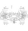
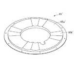
本発明のサセプタ支持部100は、一例として図1に示すように、貫通孔10を有するサセプタ20に載置した半導体ウェーハWの表面上にエピタキシャル膜を形成するエピタキシャル成長装置200内で、サセプタ20を下方から支持するものである。サセプタ支持部100は、サセプタ20を支持するサセプタシャフト110および半導体ウェーハWを支持する基板リフト部120を備える。エピタキシャル成長装置200は、その上部および下部に、ハロゲンランプ等の加熱手段210を備える。 As an example, as shown in FIG. 1, the
図2に示すように、サセプタシャフト110は、支柱111およびこの支柱111から放射状に延びる複数本の腕部112を有する。サセプタシャフト110の腕部112は、支柱111側から、第1腕部113、第1腕部113と連結する第2腕部114、および第2腕部114と連結する第3腕部115を有する。第2腕部114には、第2腕部114を鉛直方向に貫通する貫通孔116が設けられる。 As shown in FIG. 2, the
また、図3に示すように、基板リフト部120は、支柱121およびこの支柱から放射状に延びる複数本の腕部122を有する。基板リフト部120の腕部122は、支柱121側から、第1腕部123、第1腕部123と連結する第2腕部124、および第2腕部124と連結する台座部125を有する。 As shown in FIG. 3, the
図1〜図3に示すように、基板リフト部120の軸部121には、サセプタシャフト110の軸部111が挿入され、上下運動および回転が可能な構成となっている。 As shown in FIGS. 1 to 3, the
そして、図1に示されるように、台座部125と半導体ウェーハWとの間には、サセプタシャフト110の貫通孔116およびサセプタ20の貫通孔10を貫通可能なリフトピン130が設けられる。 As shown in FIG. 1,
また、図3に示すように、基板リフト部120の台座部125には、凹部126を設けるのが好ましい。この凹部126を設けることにより、リフトピンがずれて傾くことを防止し、複数のリフトピンを同じ高さで持ち上げることが可能になる。また、リフトピンが折れるのを防止することもできる。 In addition, as shown in FIG. 3, it is preferable to provide a
上述したリフトピン130により、半導体ウェーハWを相対的に上下に移動させることができる。具体的には、図4(a)の状態から図4(b)の状態にサセプタシャフト110を下方に移動させることで、サセプタ20が降下し、リフトピン130がサセプタ20の貫通孔10を貫通することで、半導体ウェーハWが相対的に持ち上がる。 The semiconductor wafer W can be relatively moved up and down by the
逆に、図4(b)の状態から図4(a)の状態にサセプタシャフト110を上方に移動させることで、サセプタ20が上昇し、半導体ウェーハWが相対的に下がり、サセプタ20上に載置される。このとき、リフトピン130が落下することのないよう、サセプタ20の貫通孔10を、下方に向かって径が小さくなるテーパ形状またはT字形状とし、リフトピン130の先端をこれに対応する形状とすることができる。 Conversely, by moving the
そして、本発明のサセプタ支持部100は、図2に示すように、サセプタシャフト110の第1腕部113の幅を、第2腕部114の幅よりも小さい構成とすることで、サセプタ支持部100がサセプタの加熱に与える影響を小さくすることができる。また、腕部の本数を減らすものではないので、同じ腕部の本数を有するサセプタ支持部と比較しても、サセプタを支持する力は劣るものではない。 As shown in FIG. 2, the
また、サセプタの加熱に与える影響をより低減するため、サセプタシャフト110の第1腕部113の幅を、貫通孔116の直径以下とするのが好ましい。 In order to further reduce the influence on the heating of the susceptor, the width of the
具体的には、サセプタシャフト110の第1腕部113の幅は、3.0mm以上6.3mm未満の範囲とするのが好ましい。幅が3.0mm未満だと、サセプタを十分に支持することができなくなるおそれがあり、幅が6.3mm以上だと、サセプタの加熱に与える影響が大きくなるおそれがあるためである。 Specifically, the width of the
同様に、サセプタシャフト110の第3腕部115の幅は、サセプタシャフト110の第2腕部114の幅よりも小さくするのが好ましい。 Similarly, the width of the
同様に、サセプタシャフト110の第3腕部115の幅は、サセプタシャフト110の貫通孔116の直径以下とするのが好ましい。 Similarly, the width of the
また、図3に示すように、サセプタの加熱に与える影響をより低減するため、基板リフト部120の第2腕部124の幅を、基板リフト部120の第1腕部123の幅よりも小さくするのが好ましい。 Further, as shown in FIG. 3, in order to further reduce the influence on the heating of the susceptor, the width of the
具体的には、前記基板リフト部120の第2腕部124の幅は、2.0mm以上4.8mm未満の範囲とするのが好ましい。幅が2.0mm未満だと、リフトピンを十分に支持することができなくなるおそれがあり、幅が4.8mm以上だと、サセプタの加熱に与える影響が大きくなるおそれがあるためである。 Specifically, the width of the
また、基板リフト部120の第2腕部124の幅は、サセプタシャフト110の第1腕部113の幅と同じにしてもよい。 Further, the width of the
また、図2に示すように、サセプタシャフト110は、支柱111と第1腕部113との間に、これら部材を連結する支柱側腕部117を有するのが好ましく、支柱側腕部117の幅は、サセプタシャフト110の第1腕部113の幅よりも大きくするのが好ましい。サセプタシャフト110の支柱111と、腕部112との連結を強くするためである。 Further, as shown in FIG. 2, the
また、サセプタシャフト110および基板リフト部120は、透明石英で形成されるのが好ましい。加熱装置210からの輻射熱をサセプタ20に十分に伝えるためである。 The
さらに、サセプタシャフト110の支柱111の上部には、サセプタ20を支持する力を高めるためのキャップを設けることも可能である。 Furthermore, a cap for increasing the force for supporting the
なお、図面では腕部の本数を3本としたが、必要に応じて増減が可能である。 In the drawing, the number of arm portions is three, but it can be increased or decreased as necessary.
続いて、本発明のエピタキシャル成長装置の実施形態について、図面を参照しながら説明する。 Next, an embodiment of the epitaxial growth apparatus of the present invention will be described with reference to the drawings.
本発明のエピタキシャル成長装置200は、一例として図1に示すように、貫通孔10を有するサセプタ20に載置した半導体ウェーハWの表面上にエピタキシャル膜を形成する。 As an example, the
エピタキシャル成長装置200は、反応室2を有する。反応室2は、基板Wが載置されるサセプタ20と、側壁部4と、天井部5とから構成される。 The
サセプタ20は、上面視において円形状の板状部材であり、基板Wより若干大きくなるように構成されている。サセプタ20には、基板Wを載置するための基板用凹部3aが設けられている。サセプタ20は、複数の腕部を有するサセプタ支持部100により支持されている。 The
サセプタ20は、成膜位置P1においてその周囲に環状のサセプタリング7が配されている。サセプタリング7は、反応室2の側壁部4に設けられたフランジ部13により支持されている。 The
天井部5は、天井板21と、天井板21を支持する支持部22とからなる。天井板21は、透過性を有するものであり、天井板21の外側上方に設けられた加熱手段210(例えばハロゲンランプ)および上部リフレクタ26からの熱を透過して反応室2内を加熱することができるように構成されている。即ち、本実施形態におけるエピタキシャル成長装置200はコールドウォールタイプのエピタキシャル成長装置である。本実施形態では、天井板21として石英を用いている。 The
天井板21を支持する支持部22は環状である。支持部22の内縁より内側の貫通穴24の基板W側の端部に天井板21が固定されている。固定方法としては、溶接が挙げられる。 The
側壁部4は、環状の上部側壁部31と、環状の下部側壁部32とからなる。下部側壁部32の内周側には、前述したフランジ部13が設けられている。この上部側壁部31の上に支持部22が配置される。 The
下側側壁部32の第1凹部34と、上側側壁部31の第1凸部36との間の間隙35は、反応ガス供給路41(供給路)として機能する。 A
同様に、下側側壁部32の第1凹部37と、上側側壁部31の第1凸部39との間の間隙38は、ガス排出路42として機能する。 Similarly, the
このように反応ガス供給路41とガス排出路42とは反応室2において対向し、反応室2において反応ガスは基板W上を水平方向に流れる。 Thus, the reaction
側壁部4の下部側壁部32の下面側には、環状の載置台45が設けられ、側壁部4が載置台45に載置されている。 An annular mounting table 45 is provided on the lower surface side of the lower
天井部5、側壁部4、載置台45の外周側には、環状の挟持部51が設けられており、環状の挟持部51は、これら天井部5、側壁部4及び載置台45をクランプして支持している。挟持部51には、それぞれ反応ガス供給路41に連通する供給側連通路52と、ガス排出路42に連通する排出側連通路53とが設けられている。供給側連通路52にはガス導入チューブ55が内挿されている。また、排出側連通路53にはガス排出チューブ58が内挿されている。 An
挟持部51の外側には、反応ガス導入部54が設けられており、反応ガス導入部54と供給側連通路52とは通路が連通している。反応ガス導入部54からは、本実施形態では、第1原料ガスと、第2原料ガスとが導入されている。なお、第2原料ガスはキャリアガスとしても機能する。反応ガスとしては3種類以上のガスを混合して用いることも可能である。供給側連通路52と反応ガス導入部54との接続部分には、ガス流路に対して垂直となるように整流板56が設けられている。整流板56には、複数の孔部56aが周方向に沿って一列に設けられており、この孔部56aを反応ガスが通過することで、第1原料ガスと第2原料ガスとが混合されると共に整流される。また、挟持部51の外側には、ガス排出部57も設けられている。ガス排出部57は、反応室2の中心を挟んで反応ガス導入部54と対向する位置に設けられている。ガス排出部57と排出側連通路53とは通路が連通している。即ち、反応ガス供給路41には、供給側連通路52を介して反応ガス導入部54が接続されている。また、ガス排出路42は、排出側連通路53を介してガス排出部57が接続されている。ガス排出路42は、反応室2の中心を挟んで反応ガス供給路41と対向するように設けられている。 A reaction
また、載置台45の内周側下部には、装置底部61が設けられている。装置底部61の外側には、別の加熱手段62および下部リフレクタ65が設けられており、基板Wを下方からも加熱することが可能である。 In addition, an apparatus bottom 61 is provided in the lower part on the inner peripheral side of the mounting table 45. Another heating means 62 and a
装置底部61の中央には、サセプタ支持部100の軸部63が挿入されると共に、パージガスが導入されるパージガス導入部(図示せず)が設けられている。パージガスは、パージガス導入部に設けられた図示しないパージガス導入手段から装置底部61、下部側壁部32及び載置台45とから構成された反応室下部64に導入される。 At the center of the apparatus bottom 61, a
サセプタ20を下方から支持するサセプタ支持部100については上述した通りである。 The
本発明の他の実施形態となるエピタキシャル成長装置200の構成について、図5、図6および図7を用いて詳細に説明する。図5はエピタキシャル成長装置200の全体を示す断面図である。また、図6はエピタキシャル成長装置200の反応室2の構成を示す分解斜視図、図7はエピタキシャル成長装置200の反応室2の外側の構成を示す分解斜視図である。 The configuration of an
エピタキシャル成長装置200は、基板W上に、例えばシリコンなどの膜をエピタキシャル成長させるための成膜装置である。 The
エピタキシャル成長装置200は反応室2を有する。反応室2は、基板Wが載置されるサセプタ20と、側壁部4と、天井部5とから構成される。 The
サセプタ20は、上面視において円形状の板状部材であり、基板Wより若干大きくなるように構成されている。サセプタ20には、基板Wを載置するための基板用凹部3aが設けられている。サセプタ20は、複数の腕部を有するサセプタ支持部100により支持されている。 The
サセプタ支持部100は、サセプタ20を支持しながらサセプタ20を昇降させる。サセプタ20の基板Wが載置される面の昇降範囲は、サセプタ20が、基板W上に成膜が行われる成膜位置P1から、基板Wのエピタキシャル成長装置200への出し入れを行う基板搬送位置P2までの間である。そして、サセプタ支持部100は、この成膜位置P1において、サセプタ支持部100の軸を回転中心として回転することによって、サセプタ20および基板Wを回転させることが可能であるように構成されている。 The
サセプタ20は、成膜位置P1においてその周囲に環状のサセプタリング7が配されている。サセプタリング7は、詳しくは後述するが、第1リング11と、第1リング11上に載置された第2リング12とからなる。サセプタリング7は、反応室2の側壁部4に設けられたフランジ部13により支持されている。 The
天井部5は、天井板21と、天井板21を支持する支持部22とからなる。天井板21は、透過性を有するものであり、天井板21の外側上方に設けられた加熱手段210(例えばハロゲンランプ)および上部リフレクタ26からの熱を透過して反応室2内を加熱することができるように構成されている。即ち、本実施形態におけるエピタキシャル成長装置200はコールドウォールタイプのエピタキシャル成長装置である。本実施形態では、天井板21として石英を用いている。 The
天井板21を支持する支持部22は環状である。支持部22の内縁より内側の貫通穴24の基板W側の端部に天井板21が固定されている。固定方法としては、溶接が挙げられる。 The
側壁部4は、環状の上部側壁部31と、環状の下部側壁部32とからなる。下部側壁部32の内周側には、前述したフランジ部13が設けられている。このフランジ部13よりも下方側に、基板搬送口30が設けられている。上部側壁部31は、その上面に、支持部22の突出部25の外側の斜面部に対応する斜面部を有している。この上部側壁部31の斜面上に支持部22が配置される。 The
下部側壁部32の上面は外周部の一部が切り欠かれ、この切り欠きが設けられていない領域は、上部側壁部31が載置される載置面33として構成されている。下部側壁部32の切り欠きにより、下部側壁部32には第1凹部34が形成されている。即ち、第1凹部34は、下部側壁部32の上面の載置面33が形成されていない部分に形成された凹部である。上部側壁部31には、下部側壁部32への載置時にこの第1凹部34に対応する位置に、第1凹部34の形状に対応し、かつ、この第1凹部34との間に間隙35が形成されるように、第1凸部36が設けられている。そして、この第1凸部36と第1凹部34との間の間隙35が反応ガス供給路41(供給路)として機能する。反応ガス供給路41については詳しくは後述する。 The upper surface of the lower
また、下部側壁部32の第1凹部34と対向する領域において、下部側壁部32の上面はその外周部の一部が切り欠かれて第2凹部37が形成されている。上部側壁部31には、下部側壁部32への載置時にこの第2凹部37に対応する位置に、第2凹部37の形状に対応し、かつ、この第2凹部37との間に間隙38が形成されるように、第2凸部39が形成されている。この第2凹部37と上部側壁部31の第2凸部39とでガス排出路42が形成されている。 Further, in the region of the lower
このように反応ガス供給路41とガス排出路42とは反応室2において対向し、反応室2において反応ガスは基板W上を水平方向に流れる。 Thus, the reaction
また、下部側壁部32の第2凹部37を構成する壁面43には、パージガスが排出されるパージ孔44が形成されている。パージ孔44は、フランジ部13よりも下方に設けられている。そして、このパージ孔44が第2凹部37を構成する壁面43に設けられていることから、パージ孔44はガス排出路42に臨んでいる。従って、ガス排出路42には、反応ガスとパージガスの両方が排出される。 A
側壁部4の下部側壁部32の下面側には、環状の載置台45が設けられ、側壁部4が載置台45に載置されている。 An annular mounting table 45 is provided on the lower surface side of the lower
天井部5、側壁部4、載置台45の外周側には、環状の挟持部51が設けられており、環状の挟持部51は、これら天井部5、側壁部4及び載置台45をクランプして支持している。挟持部51には、それぞれ反応ガス供給路41に連通する供給側連通路52と、ガス排出路42に連通する排出側連通路53とが設けられている。供給側連通路52にはガス導入チューブ55が内挿されている。また、排出側連通路53にはガス排出チューブ58が内挿されている。 An
挟持部51の外側には、反応ガス導入部54が設けられており、反応ガス導入部54と供給側連通路52とは通路が連通している。反応ガス導入部54からは、本実施形態では、第1原料ガスと、第2原料ガスとが導入されている。なお、第2原料ガスはキャリアガスとしても機能する。反応ガスとしては3種類以上のガスを混合して用いることも可能である。供給側連通路52と反応ガス導入部54との接続部分には、ガス流路に対して垂直となるように整流板56が設けられている。整流板56には、複数の孔部56aが周方向に沿って一列に設けられており、この孔部56aを反応ガスが通過することで、第1原料ガスと第2原料ガスとが混合されると共に整流される。また、挟持部51の外側には、ガス排出部57も設けられている。ガス排出部57は、反応室2の中心を挟んで反応ガス導入部54と対向する位置に設けられている。ガス排出部57と排出側連通路53とは通路が連通している。即ち、反応ガス供給路41には、供給側連通路52を介して反応ガス導入部54が接続されている。また、ガス排出路42は、排出側連通路53を介してガス排出部57が接続されている。ガス排出路42は、反応室2の中心を挟んで反応ガス供給路41と対向するように設けられている。 A reaction
また、載置台45の内周側下部には、装置底部61が設けられている。装置底部61の外側には、別の加熱手段62および下部リフレクタ65が設けられており、基板Wを下方からも加熱することが可能である。 In addition, an apparatus bottom 61 is provided in the lower part on the inner peripheral side of the mounting table 45. Another heating means 62 and a
装置底部61の中央には、サセプタ支持部100の軸部63が挿入されると共に、パージガスが導入されるパージガス導入部(図示せず)が設けられている。パージガスは、パージガス導入部に設けられた図示しないパージガス導入手段から装置底部61、下部側壁部32及び載置台45とから構成された反応室下部64に導入される。また、パージ孔44は反応室下部64に連通している。 At the center of the apparatus bottom 61, a
(エピタキシャル成長を用いた成膜方法の概要)
次に、本実施形態のエピタキシャル成長装置を用いた成膜方法について説明する。(Outline of deposition method using epitaxial growth)
Next, a film forming method using the epitaxial growth apparatus of this embodiment will be described.
まず、サセプタ20を基板搬送位置P2まで移動させ、基板Wを基板搬送口30から搬入し、サセプタ20を成膜位置P1まで移動させる。基板Wとしては、直径が例えば200mmのシリコン基板を用いる。次に、加熱手段210により待機温度(例えば、800℃)から成長温度(例えば1100℃)に加熱される。パージガス導入部からパージガス(例えば水素)を反応室下部64に導入する。また、反応ガス(例えば第1原料ガスとしてトリクロロシラン、第2原料ガスとして水素)を反応ガス導入部54から反応ガス供給路41を介して反応室2内に導入する。反応ガスは、基板Wの表面に境界層を形成し、この境界層において反応が生じる。これにより、基板W上にシリコン膜が成膜される。反応ガスは、反応室2に臨んだガス排出路42から排出される。また、パージガスはパージ孔44を介してガス排出路42へ排出される。このようにしてエピタキシャル成長が終了した後、待機温度まで降温してから、基板Wは搬出され、半導体製造装置の別のチャンバに移動される。 First, the
(エピタキシャル成長装置・方法の詳細)
次に、本実施形態のエピタキシャル成長装置200の構成部材の詳細について説明するとともに、本実施形態の成膜方法の詳細についても説明する。(Details of epitaxial growth system and method)
Next, details of the constituent members of the
図8は、本実施形態における天井部5の構成を示す斜視断面図である。図に示したように、天井板21を支持する支持部22の内縁は、基板側に向かって徐々に径が小さくなっている。そして、内縁の基板W側の端部に天井板21が固定されている。また、支持部22を裏面側(下面側)からみると、内周部が突出して突出部25となっている。この突出部25も突出方向に向かって徐々に径が小さくなるように形成されている。このように、支持部22は2つの斜面部から構成される。即ち、支持部22は、天井板21の周縁部において、周縁部の上方かつ外側から天井板21を支持する。一方、図20は、従来のエピタキシャル成長装置の天井部5’の一例を示す斜視断面図である。図に示したように、従来の装置の天井部5’では、天井板21’の周縁部において、支持部22’が、天井板21’と同一平面上から天井板21’を支持し、支持部22’は略直角の角部25’を有する形状となっている。 FIG. 8 is a perspective sectional view showing the configuration of the
このように、本実施形態では、従来のものに比べて、支持部22を応力が集中しにくい形状としていることから、基板Wと天井板21との距離Hを短く、即ち10mm未満とすることができる。 Thus, in this embodiment, since the
具体的には、天井板21(21’)を加熱手段210からの赤外線は概ね通過するが、天井板21(21’)自体はサセプタ20、又は基板Wからの輻射熱を吸収する。この吸収された熱は天井板21(21’)から支持部22(22’)との接合部を介して支持部22(22’)へ入力される。ここで、基板Wと天井板21(21’)との距離Hを短くすると、この輻射熱の吸収量が高くなり、支持部22(22’)に入力される熱が多くなる。したがって、従来の天井部5’のように、支持部22’が略直角の角部25’を有すると、この角部25’に応力が集中してしまい、割れなどが発生するおそれがある。 Specifically, the infrared rays from the heating means 210 generally pass through the ceiling plate 21 (21 '), but the ceiling plate 21 (21') itself absorbs radiant heat from the
一方、本実施形態では、支持部22に突出部25を設け、天井板21の周縁部において、周縁部の上方かつ外側から天井板21を支持させることによって、なるべく応力が集中しやすい角部(25’)を設けずに天井板21を基板側で支持することができるようしている。 On the other hand, in the present embodiment, by providing the
また、本実施形態では、上述のように境界層を狭くするために天井板21と基板Wとの距離Hを短くしているので、反応ガスが基板Wの外側に逃げてしまいやすく、基板において膜厚分布の均一化が難しい場合も考えられるので、これを防止することが好ましい。このため、本実施形態では、以下に説明するように、ガス流れを均一化するために、反応ガス供給路41にガイド部を設けている。 In the present embodiment, since the distance H between the
反応ガス供給路41に設けられたガイド部について、図9から図11を用いて詳細に説明する。前述のとおり、反応ガス供給路41は、下部側壁部32の第1凹部34と上部側壁部31の第1凸部36とから形成されて、供給側連通路52内のガス導入チューブ55を介して反応ガス導入部54まで連通している。また、反応ガス供給路41は、反応ガス導入部54からのガスの導入方向と一致する方向(水平方向)に延設された第1供給路71と、第1供給路71に連通し、ガスの導入方向に対して垂直な方向(鉛直方向)に延設された第2供給路72と、第2供給路72に連通し、ガスの導入方向に一致する方向(水平方向)に延設された第3供給路73とを有している。そして、第3供給路73は、反応室2に連通している。即ち、反応ガス供給路41は、反応ガスの入口である供給側連通路52側から、反応ガスの出口である反応室2に接続される出口に向かって上り階段状に形成されている。 The guide part provided in the reactive
ここで、第2供給路72は、上述のように鉛直方向に延設されているので、反応ガス導入部から導入されたガスが第2供給路72の反応ガス導入部54に対向する壁面74に接触する。これにより、反応ガスが拡散され、反応ガスの混合性が高まる。即ち、第2供給路72は反応ガスの混合室として機能する。この場合に、第2供給路72で反応ガスが停滞しないように、本実施形態では、第2供給路72の壁面74には、鉛直方向に延びた溝部75が形成されており、この溝部75がガイド部として機能する。このように溝部75が設けられていることで、第2供給路72の壁面74に接触することで拡散されたガスも第3供給路73へ流入しやすく、さらにこの溝部75に沿って整流されることで、反応ガスの直進性が向上して、反応室2に流入した場合の反応ガスの広がりを抑制できる。 Here, since the
溝部75について詳細に説明する。溝部75は、第2供給路72の壁面74の全面に複数本連続して凹部として形成されている。図11(a)に示すように、凹部である溝部75は、溝部75の幅方向において湾曲している。本実施形態では、溝部75は、上面視において円弧状である。溝部75が幅方向において湾曲していることから、反応ガスが、壁面74の溝部75の底部に接触した場合に、拡散しにくく(集中しやすく)、反応ガスが反応室2へ流入した場合にも基板Wの外側へより広がりにくい。なお、この溝部75の深さが深すぎると拡散を抑制することはできるが、反応ガス中の第1原料ガスと第2原料ガスとの混合をすることが難しくなる。本発明の一実施形態では、溝部75の深さは1mm〜5mmとすることが好ましい。さらに、3mmとすることがより好ましい。 The
また、溝部75は、それぞれが下部側壁部32の面内方向の中央Cに向かうように設けられている。即ち、溝部75は、下部側壁部32の周方向に沿って設けられている。このように設けることで、各溝部75によりガイドされて反応室2内に導入された反応ガスの流れの向きの水平方向の成分が、反応ガス供給路41の反応室2側の開口の中心から反応室2の中心に向かう向きの水平方向の成分と一致するように整流性が高められ、反応ガスが反応室2内で分散されてしまうことが抑制される。 Further, each of the
さらに、各溝部75の幅方向の中心と反応ガス導入部54に設けられた整流板56の孔部56aの中心とが略一致する(対応する)位置に、各溝部75は設けられている。即ち、本実施形態では壁面74における溝部75の数と孔部56aの数とは一致する。これにより、整流板56より整流された反応ガスがそのまま各溝部75に流入するので、さらに整流作用が高まり、反応ガスの直進性を向上させることができる。 Further, each
なお、本実施形態では第2供給路72の壁面74の全面に溝部75を設けたが、第2供給路72の壁面74のうち、少なくとも端部部分に設ければよい。端部部分とは、整流板56の孔部が複数の領域に分けられて設けられているが、この領域のうち、最も端部の領域に対応する部分をいう。例えば、図11(b)に示す場合では、整流板56は3つの領域81に分けられており、この領域のうち、最も端部の領域82、83の孔部に対応して溝部75が設けられていればよい。上記のように反応ガスは基板Wの外側に逃げやすいので、特に反応ガス供給路41の端部部分において反応ガスの直進性を高めるために溝部75を設けることが好ましいのである。そして、この場合にガイド部として機能する溝部75を凹部として形成することでこのような効果を簡易に得ることができる。例えば、整流部材を第2供給路72に別途設けるとなると反応ガスの混合性や製造コスト等の問題が発生するが、本実施形態のように溝部75を凹部として形成することにより、これらの問題は解決される。 In this embodiment, the
図12は、整流板56の例を示した斜視図である。図に示したように、整流板56は、溝部75のパターンに応じたものを用意すればよい。整流板56の開口率は、成長速度の観点だけでなく、スクラバーや、外部の配管の形状、長さ等の付帯設備を含めて最適な値に決定することが好ましい。 FIG. 12 is a perspective view showing an example of the
本実施形態では、上述のように境界層を狭くするために天井板21と基板Wとの距離を狭くしているので、反応室2下部への反応ガスの周りこみが発生しやすいと共に、基板Wの温度分布が均一化されにくいことが考えられ、その結果、厚膜形成時の膜厚分布や膜質の低下(例えば抵抗率の分布や結晶欠陥の発生など)も考えられる。本実施形態では、これを防止すべく、サセプタリング7が2つの部材で構成されている。この点について説明する。 In the present embodiment, as described above, the distance between the
図13に拡大して示したように、サセプタリング7を構成する第1リング11は、サセプタの外周に対して離間して設けられており、この第1リングの内周側には上面が低い段差部91が形成されている。段差部91には、第2リング12が載置されており、この第2リング12は、第1リング11とサセプタ20との間に形成された離間部92に臨んで、即ち離間部92にせり出すように設けられている。第2リング12は、その上面がサセプタ20の上面と等しくなるように設けている。このように第2リング12の上面がサセプタ20の上面と等しくなるように設けていることで、反応ガス供給路41等で混合されて整流された状態が維持された反応ガスを、速度をできるだけ低下させること無く、スムーズに基板Wに供給できる。なお、ここでいうサセプタ20の上面とは、サセプタ20の基板用凹部3a (図5,6,15,16参照)の形成されていない領域の上面をいう。本実施形態の第2リング12は、熱伝導性に鑑みてシリコンカーバイドを材料としている。 As shown in FIG. 13 in an enlarged manner, the
そして、このように第2リング12と第1リング11とを別部材で構成していることで、より精度良くサセプタリング7を構成することができる。即ち、サセプタリング7とサセプタ20との距離を限界まで近づけることができ、これにより基板Wの裏面側、即ち反応室下部64への反応ガスの回り込みを低減できると共に、基板Wの温度分布を均一化することができる。これにより、本実施形態では、形成された膜の膜厚分布や膜質分布が均一化される。 And the
また、第1リング11と第2リング12の2つの部材にすることで、第1リング11と第2リング12との間の熱の移動を第1リング11と第2リング12を1つの部材で構成する場合よりも抑制することができる。 Further, by making the
さらに、このように第2リング12が離間部92に臨むように構成されていることで、成膜時にサセプタリング7とサセプタ20との間から反応ガスが下方に漏れ出すことを低減できて、反応ガスの流れが乱れにくく、また、反応ガスが下方に漏れ出すことを低減できることから、パーティクルを低減できる。 Furthermore, since the
この場合に、第2リング12は第1リング11に比べて薄く形成してある。これにより、サセプタ20からの輻射による熱損失を抑制することができる。また、第2リング12が薄いことで、第2リング12を所定の高温に維持する(プリヒート)ために必要な加熱量を少なくすることができる。他の実施形態として、第1リング11を熱伝導率の小さい材質にした場合には、第1リング11が断熱材として機能し、上記の効果をさらに高めることができる。 In this case, the
なお、本実施形態では第2リング12が離間部92に臨むように構成したが、これに限定されない。第2リング12は、第1リング11の段差部91に少なくとも載置されるように構成されていれば、精度良くサセプタリング7を構成することができるので、サセプタリング7とサセプタ20との距離を限界まで近づけることができ、これにより基板Wの裏面側への反応ガスの回り込みを低減できると共に、基板の温度分布を均一化することができる。 In the present embodiment, the
また、本実施形態では、境界層を狭くするために天井板21と基板Wとの距離を狭くしているので、天井板21の天井面も反応ガスによりコーティングされやすい。天井面がコーティングされると、天井面が曇ってしまい、天井板21を介して加熱手段210から加熱するコールドウォールタイプのエピタキシャル成長装置では十分に成膜ができないおそれがある。これに対し、本実施形態では、上述のように反応ガス供給路41の壁面に溝部75を設け、かつ、サセプタリング7を2つの部材で構成することで、反応ガスが反応室2において滞留しにくく、その結果、コート材の付着を抑制できる。これにより、連続して十分な成膜を行うことが可能である。 In the present embodiment, since the distance between the
図14は、サセプタリング7の変形例を示したものである。本変形例では、第2リング12Aが離間部92Aを覆うように設けられている点において図13に示した実施形態とは異なる。本変形例でも、第1リング11Aは側壁部32Aのフランジ部13Aに載置されている。第2リング12Aは、この第1リング11Aの段差部91Aに載置されており、かつ、その内周側はサセプタ20Aの外周に臨んでいる。 FIG. 14 shows a modification of the
本変形例では、第2リング12Aが離間部92Aを覆うように設けられていることで、反応室2Aに流入した反応ガスが反応室下部64Aへ入ることをより抑制することができる。ただし、第2リング12Aが、図14中に図示しない加熱手段210からサセプタ20Aへの加熱を遮るのを抑制すべく、第2リング12Aとサセプタ20Aとのオーバーラップ量は少ない方が好ましい。 In the present modification, the
本変形例において、第2リング12Aの厚みは、例えば0.5mm〜2mmとすることが好ましい。さらに、約0.8mmとすることがより好ましい。このような厚みとすることで、サセプタ20Aから第2リング12Aへの輻射による熱損失を可能な限り抑制することができる。 In this modification, the thickness of the
図15および図16は、本発明の実施形態におけるサセプタ20の一例を示す平面図である。図に示したように、サセプタ20は、リフトピン130が貫通するリフトピン用の貫通孔10A,10Bが設けられている。また、図16に示したように、多数の貫通穴11Bを有していてもよい。この貫通穴11Bにより、基板をサセプタに載置した瞬間に間に挟まれた気体を逃がすことができ、基板Wが水平方向に滑ってしまうという問題を解決することができる。また、このようなサセプタ20Bを用いた場合、サセプタ20Aを用いた場合と比較すると、基板Wの膜厚分布の均一化や抵抗率分布の均一化の点で優位である。これは、貫通穴11Bの直径が小さければ小さいほど、貫通穴11Bの数が多ければ多いほど顕著である。また、開口率は4%を超えるものとするのが好ましく、また、サセプタの基板用凹部3Baのみではなく、その周囲にも貫通穴11Bを設けるのがより好ましい。 15 and 16 are plan views showing an example of the
図17は、本実施形態におけるガス排出チューブ58の一例を示した斜視断面図である。図に示したように、ガス排出チューブ58は、反応室2側からガス排出部57に向かうにしたがって開口が中央に向かって絞られて狭くなるように形成されている。これにより、排気が中央に整流され、排気効率の向上が図られている。 FIG. 17 is a perspective sectional view showing an example of the
また、図21は、従来のエピタキシャル成長装置における反応室2の外側の構成を示す分解斜視図である。図に示したように、ガス導入チューブ55と55’、ガス排出チューブ58と58’とを比較すると、本実施形態では、各々の中央部にある仕切り部が除去されている。これにより、膜厚分布に影響するガスの流れがスムーズになる。 FIG. 21 is an exploded perspective view showing a configuration outside the
なお、ガス排出路42とパージ孔44は、開口率が大きすぎると、反応ガスが反応室下部64に潜り込み、開口率が小さすぎると、パージガスが反応室2内での成膜プロセスに影響を及ぼしてしまうので、最適な値となるように開口が形成される。 Note that if the opening ratio of the
図18は、本発明の実施形態における上部リフレクタ26の一例を示す斜視図である。図に示したように、上部リフレクタ26は、加熱手段210からの熱線を反応室2の中心に向かって反射させる傾斜部26aと、加熱手段210からの熱線を鉛直下向きに反射させる平坦部26bとを有している。一方、図22は、従来のエピタキシャル成長装置における上部リフレクタ26’の一例を示す斜視図である。図に示したように、従来の上部リフレクタ26’も傾斜部26a’と平坦部26b’とを有しているが、本発明の実施形態の上部リフレクタ26とは傾斜部26aの配列が異なっている。具体的には、本発明の実施形態の上部リフレクタ26は、従来の上部リフレクタ26’の平坦部26b’の中央に傾斜部を1つ追加した配列となっている。このように、傾斜部26aと平坦部26bの面積比が所定の比率となるように、かつ、傾斜部26aと平坦部26bの分布が偏らないように、傾斜部26aと平坦部26bとを配列することにより、基板Wの温度分布の均一化が図られている。 FIG. 18 is a perspective view showing an example of the
図19は、本発明の実施形態における下部リフレクタ65の一例を示す斜視図である。図23は、従来のエピタキシャル成長装置における下部リフレクタ65’の一例を示す斜視図である。下部リフレクタ65も上部リフレクタ26と同様に、加熱手段62からの熱線を反応室2の中心に向かって反射させる傾斜部65aと、加熱手段62からの熱線を鉛直上向きに反射させる平坦部65bとを有しており、従来の下部リフレクタ65’の平坦部65b’の中央に傾斜部を1つ追加した配列となっている。このように、傾斜部65aと平坦部65bの面積比が所定の比率となるように、かつ、傾斜部65aと平坦部65bの分布が偏らないように、傾斜部65aと平坦部65bとを配列することにより、基板Wの温度分布の均一化が図られている。 FIG. 19 is a perspective view showing an example of the
かかる本実施形態のエピタキシャル成長装置によれば、支持部22が天井板21を支持することで、天井板21の中央部の反応室側の天井面と基板Wとの距離Hを10mm未満とすることができる。これにより、本実施形態におけるエピタキシャル成長装置200は、この天井板21とサセプタ20との間を流れる反応ガスにより形成される境界層が天井側に広がるのを抑制でき、結果として境界層が狭くなる。そうすると、この境界層内におけるガス速度が上昇するので、結果としてガス密度が向上し、基板W表面における反応効率を高めることができる。これにより、エピタキシャル成長装置200では、成長速度を向上させることができる。 According to the epitaxial growth apparatus of this embodiment, the
なお、本発明の一実施形態では、天井板21と基板Wとの距離Hは10mm未満であり、好ましくは天井板21と基板Wとの距離Hが10mm未満、かつ、基板Wの成膜された膜の表面から天井板21との距離を1mm以上である。この範囲とすることで、境界層を形成しつつも、反応ガスのガス流れをスムーズに行うことができる。 In one embodiment of the present invention, the distance H between the
即ち、本実施形態における反応室2では、基板Wと天井板21との距離を従来よりも短く(従来は20mm程度)することで、境界層を狭くして基板表面における反応効率を高め、結果として成長速度を向上させている。 That is, in the
・実施例1
下記に示すサイズのサセプタシャフトおよび基板リフト部を有するサセプタ支持部を用い、所定の条件で半導体ウェーハ上にエピタキシャル膜を成長させた。
記
サセプタシャフト
第1腕部の幅:3.3mm
第2腕部の幅:6.3mm
第3腕部の幅:3.2mm
貫通孔の直径:3.5mm
基板リフト部
第1腕部の幅:4.8mm
第2腕部の幅:3.0mmExample 1
An epitaxial film was grown on a semiconductor wafer under predetermined conditions using a susceptor support portion having a susceptor shaft having a size shown below and a substrate lift portion.
Susceptor shaft width of first arm: 3.3 mm
Second arm width: 6.3 mm
Third arm width: 3.2 mm
Through hole diameter: 3.5mm
Substrate lift part First arm width: 4.8mm
Second arm width: 3.0 mm
・比較例1
下記に示すサイズのサセプタシャフトおよび基板リフト部を有するサセプタ支持部を用いたこと以外は、実施例1と同じ条件で実験を行った。
記
サセプタシャフト
第1腕部の幅:6.3mm
第2腕部の幅:6.3mm
第3腕部の幅:6.3mm
貫通孔の直径:3.5mm
基板リフト部
第1腕部の幅:4.8mm
第2腕部の幅:4.8mmComparative example 1
The experiment was performed under the same conditions as in Example 1 except that a susceptor shaft having a size shown below and a susceptor support having a substrate lift were used.
Susceptor shaft width of first arm: 6.3mm
Second arm width: 6.3 mm
Third arm width: 6.3 mm
Through hole diameter: 3.5mm
Substrate lift part First arm width: 4.8mm
Second arm width: 4.8 mm
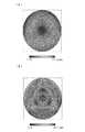
図24(a)は、実施例1のエピタキシャル膜の膜厚分布マップを示したものであり、図24(b)は比較例1のエピタキシャル膜の膜厚分布マップを示したものである。いずれも、外縁から3mmの範囲は除外し、測定点数561ポイントで膜厚を測定し、その分布を示したものである。図24(a)に示す実施例1のエピタキシャル膜の膜厚のばらつきは0.67%、図24(b)の示す比較例1のエピタキシャル膜の膜厚は1.31%であった。したがって、実施例1の本発明のサセプタシャフトを用いたエピタキシャル成長装置により形成されたエピタキシャル膜は、比較例1のものと比較して、膜厚分布が均一になっていることがわかる。 FIG. 24A shows a film thickness distribution map of the epitaxial film of Example 1, and FIG. 24B shows a film thickness distribution map of the epitaxial film of Comparative Example 1. In either case, the range of 3 mm from the outer edge is excluded, the film thickness is measured at 561 measurement points, and the distribution is shown. The variation in film thickness of the epitaxial film of Example 1 shown in FIG. 24A was 0.67%, and the film thickness of the epitaxial film of Comparative Example 1 shown in FIG. 24B was 1.31%. Therefore, it can be seen that the epitaxial film formed by the epitaxial growth apparatus using the susceptor shaft of the present invention in Example 1 has a uniform film thickness distribution as compared with that in Comparative Example 1.
100 サセプタ支持部
110 サセプタシャフト
111 支柱
112 腕部
113 第1腕部
114 第2腕部
115 第3腕部
116 貫通孔
117 支柱側腕部
120 基板リフト部
121 支柱
122 腕部
123 第1腕部
124 第2腕部
125 台座部
126 凹部
130 リフトピン
200 エピタキシャル成長装置
210 加熱手段
10 貫通孔
20 サセプタ
W 半導体ウェーハ100
Claims (9)
Translated fromJapanese該サセプタ支持部は、前記サセプタを支持するサセプタシャフトおよび前記半導体ウェーハを支持する基板リフト部を備え、
前記サセプタシャフトは、支柱および該支柱から放射状に延びる複数本の腕部を有し、
前記基板リフト部は、支柱および該支柱から放射状に延びる複数本の腕部を有し、
前記サセプタシャフトの腕部は、前記サセプタ支持部の支柱側から、第1腕部、該第1腕部と連結する第2腕部、および該第2腕部と連結する第3腕部を有し、前記第2腕部には、該第2腕部を鉛直方向に貫通する貫通孔が設けられ、
前記基板リフト部の腕部は、前記基板リフト部の支柱側から、第1腕部、該第1腕部と連結する第2腕部、および該第2腕部と連結する台座部を有し、
前記基板リフト部の台座部と前記半導体ウェーハとの間には、前記サセプタシャフトの貫通孔および前記サセプタの貫通孔を貫通可能なリフトピンが設けられ、
前記サセプタシャフトの第1腕部の幅が、前記サセプタシャフトの第2腕部の幅よりも小さいサセプタ支持部。In an epitaxial growth apparatus for forming an epitaxial film on the surface of a semiconductor wafer placed on a susceptor having a through-hole, a susceptor support part for supporting the susceptor from below,
The susceptor support portion includes a susceptor shaft that supports the susceptor and a substrate lift portion that supports the semiconductor wafer,
The susceptor shaft has a column and a plurality of arms extending radially from the column,
The substrate lift has a support and a plurality of arms extending radially from the support,
The arm portion of the susceptor shaft has a first arm portion, a second arm portion connected to the first arm portion, and a third arm portion connected to the second arm portion from the column side of the susceptor support portion. The second arm portion is provided with a through-hole penetrating the second arm portion in the vertical direction.
The arm part of the substrate lift part has a first arm part, a second arm part connected to the first arm part, and a pedestal part connected to the second arm part from the column side of the substrate lift part. ,
Between the pedestal part of the substrate lift part and the semiconductor wafer, a lift pin that can penetrate the through hole of the susceptor shaft and the through hole of the susceptor is provided,
A susceptor support portion in which a width of a first arm portion of the susceptor shaft is smaller than a width of a second arm portion of the susceptor shaft.
前記サセプタを下方から支持するサセプタ支持部を備え、
該サセプタ支持部は、前記サセプタを支持するサセプタシャフトおよび前記半導体ウェーハを支持する基板リフト部を有し、
前記サセプタシャフトは、支柱および該支柱から放射状に延びる複数本の腕部を有し、
前記基板リフト部は、支柱および該支柱から放射状に延びる複数本の腕部を有し、
前記サセプタシャフトの腕部は、前記サセプタシャフトの支柱側から、第1腕部、該第1腕部と連結する第2腕部、および該第2腕部と連結する第3腕部を有し、前記第2腕部には、該第2腕部を鉛直方向に貫通する貫通孔が設けられ、
前記基板リフト部の腕部は、前記基板リフト部の支柱側から、第1腕部、該第1腕部と連結する第2腕部、および該第2腕部と連結する台座部を有し、
前記基板リフト部の台座部と前記半導体ウェーハとの間には、前記サセプタシャフトの貫通孔および前記サセプタの貫通孔を貫通可能なリフトピンが設けられ、
前記サセプタシャフトの第1腕部の幅が、前記サセプタシャフトの第2腕部の幅よりも小さいエピタキシャル成長装置。An epitaxial growth apparatus for forming an epitaxial film on the surface of a semiconductor wafer placed on a susceptor having a through hole,
A susceptor support part for supporting the susceptor from below;
The susceptor support portion has a susceptor shaft that supports the susceptor and a substrate lift portion that supports the semiconductor wafer,
The susceptor shaft has a column and a plurality of arms extending radially from the column,
The substrate lift has a support and a plurality of arms extending radially from the support,
The arm portion of the susceptor shaft has a first arm portion, a second arm portion connected to the first arm portion, and a third arm portion connected to the second arm portion from the support column side of the susceptor shaft. The second arm portion is provided with a through-hole penetrating the second arm portion in the vertical direction.
The arm part of the substrate lift part has a first arm part, a second arm part connected to the first arm part, and a pedestal part connected to the second arm part from the column side of the substrate lift part. ,
Between the pedestal part of the substrate lift part and the semiconductor wafer, a lift pin that can penetrate the through hole of the susceptor shaft and the through hole of the susceptor is provided,
The epitaxial growth apparatus, wherein the width of the first arm portion of the susceptor shaft is smaller than the width of the second arm portion of the susceptor shaft.
Priority Applications (10)
| Application Number | Priority Date | Filing Date | Title |
|---|---|---|---|
| JP2013066897AJP5386046B1 (en) | 2013-03-27 | 2013-03-27 | Susceptor support and epitaxial growth apparatus provided with this susceptor support |
| US13/927,553US8888087B2 (en) | 2013-03-27 | 2013-06-26 | Susceptor support portion and epitaxial growth apparatus including susceptor support portion |
| CN201710619571.7ACN107578984B (en) | 2013-03-27 | 2014-03-13 | Base support and epitaxial growth apparatus including base support |
| SG10201708110XASG10201708110XA (en) | 2013-03-27 | 2014-03-13 | Susceptor support portion and epitaxial growth apparatus including susceptor support portion |
| PCT/US2014/026616WO2014160437A1 (en) | 2013-03-27 | 2014-03-13 | Susceptor support portion and epitaxial growth apparatus including susceptor support portion |
| MYPI2015001994AMY181216A (en) | 2013-03-27 | 2014-03-13 | Susceptor support portion and epitaxial growth apparatus including susceptor support portion |
| TW103109134ATWI514509B (en) | 2013-03-27 | 2014-03-13 | Susceptor support portion and epitaxial growth apparatus including susceptor support portion |
| CN201480010655.5ACN105009273B (en) | 2013-03-27 | 2014-03-13 | Base support unit and epitaxial growth equipment including base support unit |
| SG11201506255VASG11201506255VA (en) | 2013-03-27 | 2014-03-13 | Susceptor support portion and epitaxial growth apparatus including susceptor support portion |
| US14/543,451US9096949B2 (en) | 2013-03-27 | 2014-11-17 | Susceptor support portion and epitaxial growth apparatus including susceptor support portion |
Applications Claiming Priority (1)
| Application Number | Priority Date | Filing Date | Title |
|---|---|---|---|
| JP2013066897AJP5386046B1 (en) | 2013-03-27 | 2013-03-27 | Susceptor support and epitaxial growth apparatus provided with this susceptor support |
Publications (2)
| Publication Number | Publication Date |
|---|---|
| JP5386046B1true JP5386046B1 (en) | 2014-01-15 |
| JP2014192364A JP2014192364A (en) | 2014-10-06 |
Family
ID=50036625
Family Applications (1)
| Application Number | Title | Priority Date | Filing Date |
|---|---|---|---|
| JP2013066897AActiveJP5386046B1 (en) | 2013-03-27 | 2013-03-27 | Susceptor support and epitaxial growth apparatus provided with this susceptor support |
Country Status (7)
| Country | Link |
|---|---|
| US (2) | US8888087B2 (en) |
| JP (1) | JP5386046B1 (en) |
| CN (2) | CN107578984B (en) |
| MY (1) | MY181216A (en) |
| SG (2) | SG10201708110XA (en) |
| TW (1) | TWI514509B (en) |
| WO (1) | WO2014160437A1 (en) |
Cited By (3)
| Publication number | Priority date | Publication date | Assignee | Title |
|---|---|---|---|---|
| US20160033070A1 (en)* | 2014-08-01 | 2016-02-04 | Applied Materials, Inc. | Recursive pumping member |
| US10544518B2 (en)* | 2015-03-25 | 2020-01-28 | Applied Materials, Inc. | Chamber components for epitaxial growth apparatus |
| CN114830315A (en)* | 2019-12-18 | 2022-07-29 | 硅电子股份公司 | Improved apparatus for drying semiconductor substrates |
Families Citing this family (422)
| Publication number | Priority date | Publication date | Assignee | Title |
|---|---|---|---|---|
| US9394608B2 (en) | 2009-04-06 | 2016-07-19 | Asm America, Inc. | Semiconductor processing reactor and components thereof |
| US9324576B2 (en) | 2010-05-27 | 2016-04-26 | Applied Materials, Inc. | Selective etch for silicon films |
| US10283321B2 (en) | 2011-01-18 | 2019-05-07 | Applied Materials, Inc. | Semiconductor processing system and methods using capacitively coupled plasma |
| US9064815B2 (en) | 2011-03-14 | 2015-06-23 | Applied Materials, Inc. | Methods for etch of metal and metal-oxide films |
| US8999856B2 (en) | 2011-03-14 | 2015-04-07 | Applied Materials, Inc. | Methods for etch of sin films |
| US20130023129A1 (en) | 2011-07-20 | 2013-01-24 | Asm America, Inc. | Pressure transmitter for a semiconductor processing environment |
| US9267739B2 (en) | 2012-07-18 | 2016-02-23 | Applied Materials, Inc. | Pedestal with multi-zone temperature control and multiple purge capabilities |
| US9373517B2 (en) | 2012-08-02 | 2016-06-21 | Applied Materials, Inc. | Semiconductor processing with DC assisted RF power for improved control |
| US9132436B2 (en) | 2012-09-21 | 2015-09-15 | Applied Materials, Inc. | Chemical control features in wafer process equipment |
| US10714315B2 (en) | 2012-10-12 | 2020-07-14 | Asm Ip Holdings B.V. | Semiconductor reaction chamber showerhead |
| JP5343162B1 (en)* | 2012-10-26 | 2013-11-13 | エピクルー株式会社 | Epitaxial growth equipment |
| JP6053528B2 (en)* | 2013-01-11 | 2016-12-27 | 株式会社荏原製作所 | Substrate gripping device |
| US20160376700A1 (en) | 2013-02-01 | 2016-12-29 | Asm Ip Holding B.V. | System for treatment of deposition reactor |
| US10256079B2 (en) | 2013-02-08 | 2019-04-09 | Applied Materials, Inc. | Semiconductor processing systems having multiple plasma configurations |
| US10344380B2 (en) | 2013-02-11 | 2019-07-09 | Globalwafers Co., Ltd. | Liner assemblies for substrate processing systems |
| US9362130B2 (en) | 2013-03-01 | 2016-06-07 | Applied Materials, Inc. | Enhanced etching processes using remote plasma sources |
| KR102127715B1 (en)* | 2013-08-09 | 2020-06-29 | 에스케이실트론 주식회사 | An epitaxial reactor |
| US9773648B2 (en) | 2013-08-30 | 2017-09-26 | Applied Materials, Inc. | Dual discharge modes operation for remote plasma |
| US9520303B2 (en) | 2013-11-12 | 2016-12-13 | Applied Materials, Inc. | Aluminum selective etch |
| US11015245B2 (en) | 2014-03-19 | 2021-05-25 | Asm Ip Holding B.V. | Gas-phase reactor and system having exhaust plenum and components thereof |
| US9299537B2 (en) | 2014-03-20 | 2016-03-29 | Applied Materials, Inc. | Radial waveguide systems and methods for post-match control of microwaves |
| US9903020B2 (en) | 2014-03-31 | 2018-02-27 | Applied Materials, Inc. | Generation of compact alumina passivation layers on aluminum plasma equipment components |
| US9309598B2 (en) | 2014-05-28 | 2016-04-12 | Applied Materials, Inc. | Oxide and metal removal |
| US10858737B2 (en) | 2014-07-28 | 2020-12-08 | Asm Ip Holding B.V. | Showerhead assembly and components thereof |
| US9496167B2 (en) | 2014-07-31 | 2016-11-15 | Applied Materials, Inc. | Integrated bit-line airgap formation and gate stack post clean |
| US9613822B2 (en) | 2014-09-25 | 2017-04-04 | Applied Materials, Inc. | Oxide etch selectivity enhancement |
| US10941490B2 (en) | 2014-10-07 | 2021-03-09 | Asm Ip Holding B.V. | Multiple temperature range susceptor, assembly, reactor and system including the susceptor, and methods of using the same |
| US9966240B2 (en) | 2014-10-14 | 2018-05-08 | Applied Materials, Inc. | Systems and methods for internal surface conditioning assessment in plasma processing equipment |
| US9355922B2 (en) | 2014-10-14 | 2016-05-31 | Applied Materials, Inc. | Systems and methods for internal surface conditioning in plasma processing equipment |
| US11637002B2 (en) | 2014-11-26 | 2023-04-25 | Applied Materials, Inc. | Methods and systems to enhance process uniformity |
| US10224210B2 (en) | 2014-12-09 | 2019-03-05 | Applied Materials, Inc. | Plasma processing system with direct outlet toroidal plasma source |
| US10573496B2 (en) | 2014-12-09 | 2020-02-25 | Applied Materials, Inc. | Direct outlet toroidal plasma source |
| US11257693B2 (en) | 2015-01-09 | 2022-02-22 | Applied Materials, Inc. | Methods and systems to improve pedestal temperature control |
| US20160225652A1 (en) | 2015-02-03 | 2016-08-04 | Applied Materials, Inc. | Low temperature chuck for plasma processing systems |
| JP6662571B2 (en)* | 2015-02-03 | 2020-03-11 | 株式会社Sumco | Epitaxial growth apparatus and epitaxial growth method |
| US9728437B2 (en) | 2015-02-03 | 2017-08-08 | Applied Materials, Inc. | High temperature chuck for plasma processing systems |
| US9881805B2 (en) | 2015-03-02 | 2018-01-30 | Applied Materials, Inc. | Silicon selective removal |
| US10276355B2 (en) | 2015-03-12 | 2019-04-30 | Asm Ip Holding B.V. | Multi-zone reactor, system including the reactor, and method of using the same |
| CN104658959B (en)* | 2015-03-17 | 2017-07-04 | 合肥京东方光电科技有限公司 | Substrate support pin, baseplate support device and substrate clamping and placing system |
| WO2016195905A1 (en)* | 2015-05-29 | 2016-12-08 | Applied Materials, Inc. | Process chamber with reflector |
| US10458018B2 (en) | 2015-06-26 | 2019-10-29 | Asm Ip Holding B.V. | Structures including metal carbide material, devices including the structures, and methods of forming same |
| KR101730147B1 (en)* | 2015-07-23 | 2017-05-12 | 피에스케이 주식회사 | Apparatus and method for treating a substrate |
| GB201513339D0 (en)* | 2015-07-29 | 2015-09-09 | Pilkington Group Ltd | Coating apparatus |
| US9691645B2 (en) | 2015-08-06 | 2017-06-27 | Applied Materials, Inc. | Bolted wafer chuck thermal management systems and methods for wafer processing systems |
| US9741593B2 (en) | 2015-08-06 | 2017-08-22 | Applied Materials, Inc. | Thermal management systems and methods for wafer processing systems |
| US9349605B1 (en) | 2015-08-07 | 2016-05-24 | Applied Materials, Inc. | Oxide etch selectivity systems and methods |
| US10504700B2 (en) | 2015-08-27 | 2019-12-10 | Applied Materials, Inc. | Plasma etching systems and methods with secondary plasma injection |
| US10211308B2 (en) | 2015-10-21 | 2019-02-19 | Asm Ip Holding B.V. | NbMC layers |
| US11139308B2 (en) | 2015-12-29 | 2021-10-05 | Asm Ip Holding B.V. | Atomic layer deposition of III-V compounds to form V-NAND devices |
| JP6403100B2 (en)* | 2016-01-25 | 2018-10-10 | 信越半導体株式会社 | Epitaxial growth apparatus and holding member |
| US9721826B1 (en)* | 2016-01-26 | 2017-08-01 | Taiwan Semiconductor Manufacturing Co., Ltd. | Wafer supporting structure, and device and method for manufacturing semiconductor |
| US10529554B2 (en) | 2016-02-19 | 2020-01-07 | Asm Ip Holding B.V. | Method for forming silicon nitride film selectively on sidewalls or flat surfaces of trenches |
| US10343920B2 (en) | 2016-03-18 | 2019-07-09 | Asm Ip Holding B.V. | Aligned carbon nanotubes |
| CN116200821A (en)* | 2016-03-28 | 2023-06-02 | 应用材料公司 | Base support |
| US10190213B2 (en) | 2016-04-21 | 2019-01-29 | Asm Ip Holding B.V. | Deposition of metal borides |
| US10367080B2 (en) | 2016-05-02 | 2019-07-30 | Asm Ip Holding B.V. | Method of forming a germanium oxynitride film |
| US10504754B2 (en) | 2016-05-19 | 2019-12-10 | Applied Materials, Inc. | Systems and methods for improved semiconductor etching and component protection |
| US10522371B2 (en) | 2016-05-19 | 2019-12-31 | Applied Materials, Inc. | Systems and methods for improved semiconductor etching and component protection |
| US11453943B2 (en) | 2016-05-25 | 2022-09-27 | Asm Ip Holding B.V. | Method for forming carbon-containing silicon/metal oxide or nitride film by ALD using silicon precursor and hydrocarbon precursor |
| US9865484B1 (en) | 2016-06-29 | 2018-01-09 | Applied Materials, Inc. | Selective etch using material modification and RF pulsing |
| US9859151B1 (en) | 2016-07-08 | 2018-01-02 | Asm Ip Holding B.V. | Selective film deposition method to form air gaps |
| US10612137B2 (en) | 2016-07-08 | 2020-04-07 | Asm Ip Holdings B.V. | Organic reactants for atomic layer deposition |
| DE102016212780A1 (en)* | 2016-07-13 | 2018-01-18 | Siltronic Ag | Device for handling a semiconductor wafer in an epitaxial reactor and method for producing a semiconductor wafer with an epitaxial layer |
| US9887082B1 (en) | 2016-07-28 | 2018-02-06 | Asm Ip Holding B.V. | Method and apparatus for filling a gap |
| KR102532607B1 (en) | 2016-07-28 | 2023-05-15 | 에이에스엠 아이피 홀딩 비.브이. | Substrate processing apparatus and method of operating the same |
| US9812320B1 (en) | 2016-07-28 | 2017-11-07 | Asm Ip Holding B.V. | Method and apparatus for filling a gap |
| JP6551335B2 (en)* | 2016-08-01 | 2019-07-31 | 株式会社Sumco | Susceptor support shaft and epitaxial growth apparatus |
| KR101810645B1 (en) | 2016-09-08 | 2018-01-25 | 에스케이실트론 주식회사 | Chamber operating method |
| US10629473B2 (en) | 2016-09-09 | 2020-04-21 | Applied Materials, Inc. | Footing removal for nitride spacer |
| US10062575B2 (en) | 2016-09-09 | 2018-08-28 | Applied Materials, Inc. | Poly directional etch by oxidation |
| US9934942B1 (en) | 2016-10-04 | 2018-04-03 | Applied Materials, Inc. | Chamber with flow-through source |
| US9721789B1 (en) | 2016-10-04 | 2017-08-01 | Applied Materials, Inc. | Saving ion-damaged spacers |
| US10546729B2 (en) | 2016-10-04 | 2020-01-28 | Applied Materials, Inc. | Dual-channel showerhead with improved profile |
| US10062585B2 (en) | 2016-10-04 | 2018-08-28 | Applied Materials, Inc. | Oxygen compatible plasma source |
| US10062579B2 (en) | 2016-10-07 | 2018-08-28 | Applied Materials, Inc. | Selective SiN lateral recess |
| US9947549B1 (en) | 2016-10-10 | 2018-04-17 | Applied Materials, Inc. | Cobalt-containing material removal |
| US10643826B2 (en) | 2016-10-26 | 2020-05-05 | Asm Ip Holdings B.V. | Methods for thermally calibrating reaction chambers |
| US11532757B2 (en) | 2016-10-27 | 2022-12-20 | Asm Ip Holding B.V. | Deposition of charge trapping layers |
| US10714350B2 (en) | 2016-11-01 | 2020-07-14 | ASM IP Holdings, B.V. | Methods for forming a transition metal niobium nitride film on a substrate by atomic layer deposition and related semiconductor device structures |
| US9768034B1 (en) | 2016-11-11 | 2017-09-19 | Applied Materials, Inc. | Removal methods for high aspect ratio structures |
| US10163696B2 (en) | 2016-11-11 | 2018-12-25 | Applied Materials, Inc. | Selective cobalt removal for bottom up gapfill |
| US10026621B2 (en) | 2016-11-14 | 2018-07-17 | Applied Materials, Inc. | SiN spacer profile patterning |
| US10242908B2 (en) | 2016-11-14 | 2019-03-26 | Applied Materials, Inc. | Airgap formation with damage-free copper |
| KR102546317B1 (en) | 2016-11-15 | 2023-06-21 | 에이에스엠 아이피 홀딩 비.브이. | Gas supply unit and substrate processing apparatus including the same |
| KR102762543B1 (en) | 2016-12-14 | 2025-02-05 | 에이에스엠 아이피 홀딩 비.브이. | Substrate processing apparatus |
| US11447861B2 (en) | 2016-12-15 | 2022-09-20 | Asm Ip Holding B.V. | Sequential infiltration synthesis apparatus and a method of forming a patterned structure |
| US11581186B2 (en) | 2016-12-15 | 2023-02-14 | Asm Ip Holding B.V. | Sequential infiltration synthesis apparatus |
| KR102700194B1 (en) | 2016-12-19 | 2024-08-28 | 에이에스엠 아이피 홀딩 비.브이. | Substrate processing apparatus |
| US10269558B2 (en) | 2016-12-22 | 2019-04-23 | Asm Ip Holding B.V. | Method of forming a structure on a substrate |
| US10566206B2 (en) | 2016-12-27 | 2020-02-18 | Applied Materials, Inc. | Systems and methods for anisotropic material breakthrough |
| US10867788B2 (en) | 2016-12-28 | 2020-12-15 | Asm Ip Holding B.V. | Method of forming a structure on a substrate |
| US11390950B2 (en) | 2017-01-10 | 2022-07-19 | Asm Ip Holding B.V. | Reactor system and method to reduce residue buildup during a film deposition process |
| US10431429B2 (en) | 2017-02-03 | 2019-10-01 | Applied Materials, Inc. | Systems and methods for radial and azimuthal control of plasma uniformity |
| US10403507B2 (en) | 2017-02-03 | 2019-09-03 | Applied Materials, Inc. | Shaped etch profile with oxidation |
| US10043684B1 (en) | 2017-02-06 | 2018-08-07 | Applied Materials, Inc. | Self-limiting atomic thermal etching systems and methods |
| US10319739B2 (en) | 2017-02-08 | 2019-06-11 | Applied Materials, Inc. | Accommodating imperfectly aligned memory holes |
| US10468261B2 (en) | 2017-02-15 | 2019-11-05 | Asm Ip Holding B.V. | Methods for forming a metallic film on a substrate by cyclical deposition and related semiconductor device structures |
| US10943834B2 (en) | 2017-03-13 | 2021-03-09 | Applied Materials, Inc. | Replacement contact process |
| US10529563B2 (en) | 2017-03-29 | 2020-01-07 | Asm Ip Holdings B.V. | Method for forming doped metal oxide films on a substrate by cyclical deposition and related semiconductor device structures |
| US10319649B2 (en) | 2017-04-11 | 2019-06-11 | Applied Materials, Inc. | Optical emission spectroscopy (OES) for remote plasma monitoring |
| KR102457289B1 (en) | 2017-04-25 | 2022-10-21 | 에이에스엠 아이피 홀딩 비.브이. | Method for depositing a thin film and manufacturing a semiconductor device |
| US10892156B2 (en) | 2017-05-08 | 2021-01-12 | Asm Ip Holding B.V. | Methods for forming a silicon nitride film on a substrate and related semiconductor device structures |
| US10770286B2 (en) | 2017-05-08 | 2020-09-08 | Asm Ip Holdings B.V. | Methods for selectively forming a silicon nitride film on a substrate and related semiconductor device structures |
| US11276590B2 (en) | 2017-05-17 | 2022-03-15 | Applied Materials, Inc. | Multi-zone semiconductor substrate supports |
| JP7176860B6 (en) | 2017-05-17 | 2022-12-16 | アプライド マテリアルズ インコーポレイテッド | Semiconductor processing chamber to improve precursor flow |
| US11276559B2 (en) | 2017-05-17 | 2022-03-15 | Applied Materials, Inc. | Semiconductor processing chamber for multiple precursor flow |
| US10049891B1 (en) | 2017-05-31 | 2018-08-14 | Applied Materials, Inc. | Selective in situ cobalt residue removal |
| US10497579B2 (en) | 2017-05-31 | 2019-12-03 | Applied Materials, Inc. | Water-free etching methods |
| US10886123B2 (en) | 2017-06-02 | 2021-01-05 | Asm Ip Holding B.V. | Methods for forming low temperature semiconductor layers and related semiconductor device structures |
| US10920320B2 (en) | 2017-06-16 | 2021-02-16 | Applied Materials, Inc. | Plasma health determination in semiconductor substrate processing reactors |
| US12040200B2 (en) | 2017-06-20 | 2024-07-16 | Asm Ip Holding B.V. | Semiconductor processing apparatus and methods for calibrating a semiconductor processing apparatus |
| US10541246B2 (en) | 2017-06-26 | 2020-01-21 | Applied Materials, Inc. | 3D flash memory cells which discourage cross-cell electrical tunneling |
| US11306395B2 (en) | 2017-06-28 | 2022-04-19 | Asm Ip Holding B.V. | Methods for depositing a transition metal nitride film on a substrate by atomic layer deposition and related deposition apparatus |
| US10727080B2 (en) | 2017-07-07 | 2020-07-28 | Applied Materials, Inc. | Tantalum-containing material removal |
| US10541184B2 (en) | 2017-07-11 | 2020-01-21 | Applied Materials, Inc. | Optical emission spectroscopic techniques for monitoring etching |
| US10354889B2 (en) | 2017-07-17 | 2019-07-16 | Applied Materials, Inc. | Non-halogen etching of silicon-containing materials |
| KR20190009245A (en) | 2017-07-18 | 2019-01-28 | 에이에스엠 아이피 홀딩 비.브이. | Methods for forming a semiconductor device structure and related semiconductor device structures |
| US11374112B2 (en) | 2017-07-19 | 2022-06-28 | Asm Ip Holding B.V. | Method for depositing a group IV semiconductor and related semiconductor device structures |
| US11018002B2 (en) | 2017-07-19 | 2021-05-25 | Asm Ip Holding B.V. | Method for selectively depositing a Group IV semiconductor and related semiconductor device structures |
| US10541333B2 (en) | 2017-07-19 | 2020-01-21 | Asm Ip Holding B.V. | Method for depositing a group IV semiconductor and related semiconductor device structures |
| US10590535B2 (en) | 2017-07-26 | 2020-03-17 | Asm Ip Holdings B.V. | Chemical treatment, deposition and/or infiltration apparatus and method for using the same |
| TWI815813B (en) | 2017-08-04 | 2023-09-21 | 荷蘭商Asm智慧財產控股公司 | Showerhead assembly for distributing a gas within a reaction chamber |
| US10043674B1 (en) | 2017-08-04 | 2018-08-07 | Applied Materials, Inc. | Germanium etching systems and methods |
| US10170336B1 (en) | 2017-08-04 | 2019-01-01 | Applied Materials, Inc. | Methods for anisotropic control of selective silicon removal |
| US10297458B2 (en) | 2017-08-07 | 2019-05-21 | Applied Materials, Inc. | Process window widening using coated parts in plasma etch processes |
| US10770336B2 (en)* | 2017-08-08 | 2020-09-08 | Asm Ip Holding B.V. | Substrate lift mechanism and reactor including same |
| US10692741B2 (en) | 2017-08-08 | 2020-06-23 | Asm Ip Holdings B.V. | Radiation shield |
| US11769682B2 (en) | 2017-08-09 | 2023-09-26 | Asm Ip Holding B.V. | Storage apparatus for storing cassettes for substrates and processing apparatus equipped therewith |
| US11139191B2 (en) | 2017-08-09 | 2021-10-05 | Asm Ip Holding B.V. | Storage apparatus for storing cassettes for substrates and processing apparatus equipped therewith |
| TWI754765B (en)* | 2017-08-25 | 2022-02-11 | 美商應用材料股份有限公司 | Inject assembly for epitaxial deposition processes |
| US11830730B2 (en) | 2017-08-29 | 2023-11-28 | Asm Ip Holding B.V. | Layer forming method and apparatus |
| KR102491945B1 (en) | 2017-08-30 | 2023-01-26 | 에이에스엠 아이피 홀딩 비.브이. | Substrate processing apparatus |
| US11056344B2 (en) | 2017-08-30 | 2021-07-06 | Asm Ip Holding B.V. | Layer forming method |
| US11295980B2 (en) | 2017-08-30 | 2022-04-05 | Asm Ip Holding B.V. | Methods for depositing a molybdenum metal film over a dielectric surface of a substrate by a cyclical deposition process and related semiconductor device structures |
| KR102401446B1 (en) | 2017-08-31 | 2022-05-24 | 에이에스엠 아이피 홀딩 비.브이. | Substrate processing apparatus |
| KR102630301B1 (en) | 2017-09-21 | 2024-01-29 | 에이에스엠 아이피 홀딩 비.브이. | Method of sequential infiltration synthesis treatment of infiltrateable material and structures and devices formed using same |
| US10844484B2 (en) | 2017-09-22 | 2020-11-24 | Asm Ip Holding B.V. | Apparatus for dispensing a vapor phase reactant to a reaction chamber and related methods |
| US10658205B2 (en) | 2017-09-28 | 2020-05-19 | Asm Ip Holdings B.V. | Chemical dispensing apparatus and methods for dispensing a chemical to a reaction chamber |
| US10403504B2 (en) | 2017-10-05 | 2019-09-03 | Asm Ip Holding B.V. | Method for selectively depositing a metallic film on a substrate |
| US10128086B1 (en) | 2017-10-24 | 2018-11-13 | Applied Materials, Inc. | Silicon pretreatment for nitride removal |
| US10283324B1 (en) | 2017-10-24 | 2019-05-07 | Applied Materials, Inc. | Oxygen treatment for nitride etching |
| US10923344B2 (en) | 2017-10-30 | 2021-02-16 | Asm Ip Holding B.V. | Methods for forming a semiconductor structure and related semiconductor structures |
| US10910262B2 (en) | 2017-11-16 | 2021-02-02 | Asm Ip Holding B.V. | Method of selectively depositing a capping layer structure on a semiconductor device structure |
| US11022879B2 (en) | 2017-11-24 | 2021-06-01 | Asm Ip Holding B.V. | Method of forming an enhanced unexposed photoresist layer |
| CN111344522B (en) | 2017-11-27 | 2022-04-12 | 阿斯莫Ip控股公司 | Including clean mini-environment device |
| WO2019103613A1 (en) | 2017-11-27 | 2019-05-31 | Asm Ip Holding B.V. | A storage device for storing wafer cassettes for use with a batch furnace |
| US10256112B1 (en) | 2017-12-08 | 2019-04-09 | Applied Materials, Inc. | Selective tungsten removal |
| US10903054B2 (en) | 2017-12-19 | 2021-01-26 | Applied Materials, Inc. | Multi-zone gas distribution systems and methods |
| US11328909B2 (en) | 2017-12-22 | 2022-05-10 | Applied Materials, Inc. | Chamber conditioning and removal processes |
| JP6838569B2 (en)* | 2018-01-04 | 2021-03-03 | 信越半導体株式会社 | Wafer processing equipment and manufacturing method of epitaxial wafer |
| US10854426B2 (en) | 2018-01-08 | 2020-12-01 | Applied Materials, Inc. | Metal recess for semiconductor structures |
| US10872771B2 (en) | 2018-01-16 | 2020-12-22 | Asm Ip Holding B. V. | Method for depositing a material film on a substrate within a reaction chamber by a cyclical deposition process and related device structures |
| KR102695659B1 (en) | 2018-01-19 | 2024-08-14 | 에이에스엠 아이피 홀딩 비.브이. | Method for depositing a gap filling layer by plasma assisted deposition |
| TWI799494B (en) | 2018-01-19 | 2023-04-21 | 荷蘭商Asm 智慧財產控股公司 | Deposition method |
| US11018047B2 (en) | 2018-01-25 | 2021-05-25 | Asm Ip Holding B.V. | Hybrid lift pin |
| USD880437S1 (en) | 2018-02-01 | 2020-04-07 | Asm Ip Holding B.V. | Gas supply plate for semiconductor manufacturing apparatus |
| US11081345B2 (en) | 2018-02-06 | 2021-08-03 | Asm Ip Holding B.V. | Method of post-deposition treatment for silicon oxide film |
| WO2019158960A1 (en) | 2018-02-14 | 2019-08-22 | Asm Ip Holding B.V. | A method for depositing a ruthenium-containing film on a substrate by a cyclical deposition process |
| US10896820B2 (en) | 2018-02-14 | 2021-01-19 | Asm Ip Holding B.V. | Method for depositing a ruthenium-containing film on a substrate by a cyclical deposition process |
| US10679870B2 (en) | 2018-02-15 | 2020-06-09 | Applied Materials, Inc. | Semiconductor processing chamber multistage mixing apparatus |
| US10964512B2 (en) | 2018-02-15 | 2021-03-30 | Applied Materials, Inc. | Semiconductor processing chamber multistage mixing apparatus and methods |
| US10731249B2 (en) | 2018-02-15 | 2020-08-04 | Asm Ip Holding B.V. | Method of forming a transition metal containing film on a substrate by a cyclical deposition process, a method for supplying a transition metal halide compound to a reaction chamber, and related vapor deposition apparatus |
| KR102636427B1 (en) | 2018-02-20 | 2024-02-13 | 에이에스엠 아이피 홀딩 비.브이. | Substrate processing method and apparatus |
| US10975470B2 (en) | 2018-02-23 | 2021-04-13 | Asm Ip Holding B.V. | Apparatus for detecting or monitoring for a chemical precursor in a high temperature environment |
| TWI766433B (en) | 2018-02-28 | 2022-06-01 | 美商應用材料股份有限公司 | Systems and methods to form airgaps |
| US10593560B2 (en) | 2018-03-01 | 2020-03-17 | Applied Materials, Inc. | Magnetic induction plasma source for semiconductor processes and equipment |
| US11473195B2 (en) | 2018-03-01 | 2022-10-18 | Asm Ip Holding B.V. | Semiconductor processing apparatus and a method for processing a substrate |
| US11629406B2 (en) | 2018-03-09 | 2023-04-18 | Asm Ip Holding B.V. | Semiconductor processing apparatus comprising one or more pyrometers for measuring a temperature of a substrate during transfer of the substrate |
| US10319600B1 (en) | 2018-03-12 | 2019-06-11 | Applied Materials, Inc. | Thermal silicon etch |
| US10497573B2 (en) | 2018-03-13 | 2019-12-03 | Applied Materials, Inc. | Selective atomic layer etching of semiconductor materials |
| US11114283B2 (en) | 2018-03-16 | 2021-09-07 | Asm Ip Holding B.V. | Reactor, system including the reactor, and methods of manufacturing and using same |
| KR102646467B1 (en) | 2018-03-27 | 2024-03-11 | 에이에스엠 아이피 홀딩 비.브이. | Method of forming an electrode on a substrate and a semiconductor device structure including an electrode |
| US11230766B2 (en) | 2018-03-29 | 2022-01-25 | Asm Ip Holding B.V. | Substrate processing apparatus and method |
| US11088002B2 (en) | 2018-03-29 | 2021-08-10 | Asm Ip Holding B.V. | Substrate rack and a substrate processing system and method |
| KR102501472B1 (en) | 2018-03-30 | 2023-02-20 | 에이에스엠 아이피 홀딩 비.브이. | Substrate processing method |
| US10573527B2 (en) | 2018-04-06 | 2020-02-25 | Applied Materials, Inc. | Gas-phase selective etching systems and methods |
| KR102600229B1 (en) | 2018-04-09 | 2023-11-10 | 에이에스엠 아이피 홀딩 비.브이. | Substrate supporting device, substrate processing apparatus including the same and substrate processing method |
| US10490406B2 (en) | 2018-04-10 | 2019-11-26 | Appled Materials, Inc. | Systems and methods for material breakthrough |
| US10699879B2 (en) | 2018-04-17 | 2020-06-30 | Applied Materials, Inc. | Two piece electrode assembly with gap for plasma control |
| US10886137B2 (en) | 2018-04-30 | 2021-01-05 | Applied Materials, Inc. | Selective nitride removal |
| US12025484B2 (en) | 2018-05-08 | 2024-07-02 | Asm Ip Holding B.V. | Thin film forming method |
| TWI811348B (en) | 2018-05-08 | 2023-08-11 | 荷蘭商Asm 智慧財產控股公司 | Methods for depositing an oxide film on a substrate by a cyclical deposition process and related device structures |
| US12272527B2 (en) | 2018-05-09 | 2025-04-08 | Asm Ip Holding B.V. | Apparatus for use with hydrogen radicals and method of using same |
| KR20190129718A (en) | 2018-05-11 | 2019-11-20 | 에이에스엠 아이피 홀딩 비.브이. | Methods for forming a doped metal carbide film on a substrate and related semiconductor device structures |
| KR102596988B1 (en) | 2018-05-28 | 2023-10-31 | 에이에스엠 아이피 홀딩 비.브이. | Method of processing a substrate and a device manufactured by the same |
| US11718913B2 (en) | 2018-06-04 | 2023-08-08 | Asm Ip Holding B.V. | Gas distribution system and reactor system including same |
| TWI840362B (en) | 2018-06-04 | 2024-05-01 | 荷蘭商Asm Ip私人控股有限公司 | Wafer handling chamber with moisture reduction |
| US11286562B2 (en) | 2018-06-08 | 2022-03-29 | Asm Ip Holding B.V. | Gas-phase chemical reactor and method of using same |
| KR102568797B1 (en) | 2018-06-21 | 2023-08-21 | 에이에스엠 아이피 홀딩 비.브이. | Substrate processing system |
| US10797133B2 (en) | 2018-06-21 | 2020-10-06 | Asm Ip Holding B.V. | Method for depositing a phosphorus doped silicon arsenide film and related semiconductor device structures |
| KR102854019B1 (en) | 2018-06-27 | 2025-09-02 | 에이에스엠 아이피 홀딩 비.브이. | Periodic deposition method for forming a metal-containing material and films and structures comprising the metal-containing material |
| TWI873894B (en) | 2018-06-27 | 2025-02-21 | 荷蘭商Asm Ip私人控股有限公司 | Cyclic deposition methods for forming metal-containing material and films and structures including the metal-containing material |
| US10612136B2 (en) | 2018-06-29 | 2020-04-07 | ASM IP Holding, B.V. | Temperature-controlled flange and reactor system including same |
| KR102686758B1 (en) | 2018-06-29 | 2024-07-18 | 에이에스엠 아이피 홀딩 비.브이. | Method for depositing a thin film and manufacturing a semiconductor device |
| US10755922B2 (en) | 2018-07-03 | 2020-08-25 | Asm Ip Holding B.V. | Method for depositing silicon-free carbon-containing film as gap-fill layer by pulse plasma-assisted deposition |
| US10388513B1 (en) | 2018-07-03 | 2019-08-20 | Asm Ip Holding B.V. | Method for depositing silicon-free carbon-containing film as gap-fill layer by pulse plasma-assisted deposition |
| US10872778B2 (en) | 2018-07-06 | 2020-12-22 | Applied Materials, Inc. | Systems and methods utilizing solid-phase etchants |
| US10755941B2 (en) | 2018-07-06 | 2020-08-25 | Applied Materials, Inc. | Self-limiting selective etching systems and methods |
| CN109244030B (en)* | 2018-07-09 | 2024-08-20 | 浙江求是创芯半导体设备有限公司 | Multifunctional wafer substrate base for epitaxial growth device |
| US10672642B2 (en) | 2018-07-24 | 2020-06-02 | Applied Materials, Inc. | Systems and methods for pedestal configuration |
| US11053591B2 (en) | 2018-08-06 | 2021-07-06 | Asm Ip Holding B.V. | Multi-port gas injection system and reactor system including same |
| US10883175B2 (en) | 2018-08-09 | 2021-01-05 | Asm Ip Holding B.V. | Vertical furnace for processing substrates and a liner for use therein |
| US11430674B2 (en) | 2018-08-22 | 2022-08-30 | Asm Ip Holding B.V. | Sensor array, apparatus for dispensing a vapor phase reactant to a reaction chamber and related methods |
| US11024523B2 (en) | 2018-09-11 | 2021-06-01 | Asm Ip Holding B.V. | Substrate processing apparatus and method |
| KR102707956B1 (en) | 2018-09-11 | 2024-09-19 | 에이에스엠 아이피 홀딩 비.브이. | Method for deposition of a thin film |
| US11049751B2 (en) | 2018-09-14 | 2021-06-29 | Asm Ip Holding B.V. | Cassette supply system to store and handle cassettes and processing apparatus equipped therewith |
| US10892198B2 (en) | 2018-09-14 | 2021-01-12 | Applied Materials, Inc. | Systems and methods for improved performance in semiconductor processing |
| US11049755B2 (en) | 2018-09-14 | 2021-06-29 | Applied Materials, Inc. | Semiconductor substrate supports with embedded RF shield |
| US11062887B2 (en) | 2018-09-17 | 2021-07-13 | Applied Materials, Inc. | High temperature RF heater pedestals |
| US11417534B2 (en) | 2018-09-21 | 2022-08-16 | Applied Materials, Inc. | Selective material removal |
| CN110970344B (en) | 2018-10-01 | 2024-10-25 | Asmip控股有限公司 | Substrate holding apparatus, system comprising the same and method of using the same |
| US11232963B2 (en) | 2018-10-03 | 2022-01-25 | Asm Ip Holding B.V. | Substrate processing apparatus and method |
| KR102592699B1 (en) | 2018-10-08 | 2023-10-23 | 에이에스엠 아이피 홀딩 비.브이. | Substrate support unit and apparatuses for depositing thin film and processing the substrate including the same |
| US11682560B2 (en) | 2018-10-11 | 2023-06-20 | Applied Materials, Inc. | Systems and methods for hafnium-containing film removal |
| KR102546322B1 (en) | 2018-10-19 | 2023-06-21 | 에이에스엠 아이피 홀딩 비.브이. | Substrate processing apparatus and substrate processing method |
| KR102605121B1 (en)* | 2018-10-19 | 2023-11-23 | 에이에스엠 아이피 홀딩 비.브이. | Substrate processing apparatus and substrate processing method |
| USD948463S1 (en) | 2018-10-24 | 2022-04-12 | Asm Ip Holding B.V. | Susceptor for semiconductor substrate supporting apparatus |
| US11121002B2 (en) | 2018-10-24 | 2021-09-14 | Applied Materials, Inc. | Systems and methods for etching metals and metal derivatives |
| US12378665B2 (en) | 2018-10-26 | 2025-08-05 | Asm Ip Holding B.V. | High temperature coatings for a preclean and etch apparatus and related methods |
| US11087997B2 (en) | 2018-10-31 | 2021-08-10 | Asm Ip Holding B.V. | Substrate processing apparatus for processing substrates |
| KR102748291B1 (en) | 2018-11-02 | 2024-12-31 | 에이에스엠 아이피 홀딩 비.브이. | Substrate support unit and substrate processing apparatus including the same |
| US11572620B2 (en) | 2018-11-06 | 2023-02-07 | Asm Ip Holding B.V. | Methods for selectively depositing an amorphous silicon film on a substrate |
| US11031242B2 (en) | 2018-11-07 | 2021-06-08 | Asm Ip Holding B.V. | Methods for depositing a boron doped silicon germanium film |
| US10847366B2 (en) | 2018-11-16 | 2020-11-24 | Asm Ip Holding B.V. | Methods for depositing a transition metal chalcogenide film on a substrate by a cyclical deposition process |
| US10818758B2 (en) | 2018-11-16 | 2020-10-27 | Asm Ip Holding B.V. | Methods for forming a metal silicate film on a substrate in a reaction chamber and related semiconductor device structures |
| CN109536928B (en)* | 2018-11-23 | 2020-10-09 | 中国科学院半导体研究所 | Pallet Support and Fixtures |
| US11437242B2 (en) | 2018-11-27 | 2022-09-06 | Applied Materials, Inc. | Selective removal of silicon-containing materials |
| US12040199B2 (en) | 2018-11-28 | 2024-07-16 | Asm Ip Holding B.V. | Substrate processing apparatus for processing substrates |
| US11217444B2 (en) | 2018-11-30 | 2022-01-04 | Asm Ip Holding B.V. | Method for forming an ultraviolet radiation responsive metal oxide-containing film |
| KR102636428B1 (en) | 2018-12-04 | 2024-02-13 | 에이에스엠 아이피 홀딩 비.브이. | A method for cleaning a substrate processing apparatus |
| US11158513B2 (en) | 2018-12-13 | 2021-10-26 | Asm Ip Holding B.V. | Methods for forming a rhenium-containing film on a substrate by a cyclical deposition process and related semiconductor device structures |
| TWI874340B (en) | 2018-12-14 | 2025-03-01 | 荷蘭商Asm Ip私人控股有限公司 | Method of forming device structure, structure formed by the method and system for performing the method |
| US11721527B2 (en) | 2019-01-07 | 2023-08-08 | Applied Materials, Inc. | Processing chamber mixing systems |
| US10920319B2 (en) | 2019-01-11 | 2021-02-16 | Applied Materials, Inc. | Ceramic showerheads with conductive electrodes |
| TWI866480B (en) | 2019-01-17 | 2024-12-11 | 荷蘭商Asm Ip 私人控股有限公司 | Methods of forming a transition metal containing film on a substrate by a cyclical deposition process |
| KR102727227B1 (en) | 2019-01-22 | 2024-11-07 | 에이에스엠 아이피 홀딩 비.브이. | Semiconductor processing device |
| CN111524788B (en) | 2019-02-01 | 2023-11-24 | Asm Ip私人控股有限公司 | Method for forming topologically selective films of silicon oxide |
| TWI838458B (en) | 2019-02-20 | 2024-04-11 | 荷蘭商Asm Ip私人控股有限公司 | Apparatus and methods for plug fill deposition in 3-d nand applications |
| TWI873122B (en) | 2019-02-20 | 2025-02-21 | 荷蘭商Asm Ip私人控股有限公司 | Method of filling a recess formed within a surface of a substrate, semiconductor structure formed according to the method, and semiconductor processing apparatus |
| TWI845607B (en) | 2019-02-20 | 2024-06-21 | 荷蘭商Asm Ip私人控股有限公司 | Cyclical deposition method and apparatus for filling a recess formed within a substrate surface |
| KR102626263B1 (en) | 2019-02-20 | 2024-01-16 | 에이에스엠 아이피 홀딩 비.브이. | Cyclical deposition method including treatment step and apparatus for same |
| TWI842826B (en) | 2019-02-22 | 2024-05-21 | 荷蘭商Asm Ip私人控股有限公司 | Substrate processing apparatus and method for processing substrate |
| KR102858005B1 (en) | 2019-03-08 | 2025-09-09 | 에이에스엠 아이피 홀딩 비.브이. | Method for Selective Deposition of Silicon Nitride Layer and Structure Including Selectively-Deposited Silicon Nitride Layer |
| US11742198B2 (en) | 2019-03-08 | 2023-08-29 | Asm Ip Holding B.V. | Structure including SiOCN layer and method of forming same |
| KR102782593B1 (en) | 2019-03-08 | 2025-03-14 | 에이에스엠 아이피 홀딩 비.브이. | Structure Including SiOC Layer and Method of Forming Same |
| JP2020167398A (en) | 2019-03-28 | 2020-10-08 | エーエスエム・アイピー・ホールディング・ベー・フェー | Door openers and substrate processing equipment provided with door openers |
| KR102809999B1 (en) | 2019-04-01 | 2025-05-19 | 에이에스엠 아이피 홀딩 비.브이. | Method of manufacturing semiconductor device |
| KR20200123380A (en) | 2019-04-19 | 2020-10-29 | 에이에스엠 아이피 홀딩 비.브이. | Layer forming method and apparatus |
| KR20200125453A (en) | 2019-04-24 | 2020-11-04 | 에이에스엠 아이피 홀딩 비.브이. | Gas-phase reactor system and method of using same |
| US11289326B2 (en) | 2019-05-07 | 2022-03-29 | Asm Ip Holding B.V. | Method for reforming amorphous carbon polymer film |
| KR20200130121A (en) | 2019-05-07 | 2020-11-18 | 에이에스엠 아이피 홀딩 비.브이. | Chemical source vessel with dip tube |
| KR20200130652A (en) | 2019-05-10 | 2020-11-19 | 에이에스엠 아이피 홀딩 비.브이. | Method of depositing material onto a surface and structure formed according to the method |
| JP7612342B2 (en) | 2019-05-16 | 2025-01-14 | エーエスエム・アイピー・ホールディング・ベー・フェー | Wafer boat handling apparatus, vertical batch furnace and method |
| JP7598201B2 (en) | 2019-05-16 | 2024-12-11 | エーエスエム・アイピー・ホールディング・ベー・フェー | Wafer boat handling apparatus, vertical batch furnace and method |
| USD947913S1 (en) | 2019-05-17 | 2022-04-05 | Asm Ip Holding B.V. | Susceptor shaft |
| USD975665S1 (en) | 2019-05-17 | 2023-01-17 | Asm Ip Holding B.V. | Susceptor shaft |
| USD935572S1 (en) | 2019-05-24 | 2021-11-09 | Asm Ip Holding B.V. | Gas channel plate |
| USD922229S1 (en) | 2019-06-05 | 2021-06-15 | Asm Ip Holding B.V. | Device for controlling a temperature of a gas supply unit |
| KR20200141002A (en) | 2019-06-06 | 2020-12-17 | 에이에스엠 아이피 홀딩 비.브이. | Method of using a gas-phase reactor system including analyzing exhausted gas |
| KR20200141931A (en) | 2019-06-10 | 2020-12-21 | 에이에스엠 아이피 홀딩 비.브이. | Method for cleaning quartz epitaxial chambers |
| KR20200143254A (en) | 2019-06-11 | 2020-12-23 | 에이에스엠 아이피 홀딩 비.브이. | Method of forming an electronic structure using an reforming gas, system for performing the method, and structure formed using the method |
| USD944946S1 (en) | 2019-06-14 | 2022-03-01 | Asm Ip Holding B.V. | Shower plate |
| USD931978S1 (en) | 2019-06-27 | 2021-09-28 | Asm Ip Holding B.V. | Showerhead vacuum transport |
| KR20210005515A (en) | 2019-07-03 | 2021-01-14 | 에이에스엠 아이피 홀딩 비.브이. | Temperature control assembly for substrate processing apparatus and method of using same |
| KR102640172B1 (en) | 2019-07-03 | 2024-02-23 | 삼성전자주식회사 | Processing apparatus for a substrate and method of driving the same |
| JP7499079B2 (en) | 2019-07-09 | 2024-06-13 | エーエスエム・アイピー・ホールディング・ベー・フェー | Plasma device using coaxial waveguide and substrate processing method |
| CN112216646A (en) | 2019-07-10 | 2021-01-12 | Asm Ip私人控股有限公司 | Substrate supporting assembly and substrate processing device comprising same |
| US11032945B2 (en)* | 2019-07-12 | 2021-06-08 | Applied Materials, Inc. | Heat shield assembly for an epitaxy chamber |
| KR20210010307A (en) | 2019-07-16 | 2021-01-27 | 에이에스엠 아이피 홀딩 비.브이. | Substrate processing apparatus |
| KR20210010816A (en) | 2019-07-17 | 2021-01-28 | 에이에스엠 아이피 홀딩 비.브이. | Radical assist ignition plasma system and method |
| KR102860110B1 (en) | 2019-07-17 | 2025-09-16 | 에이에스엠 아이피 홀딩 비.브이. | Methods of forming silicon germanium structures |
| US11643724B2 (en) | 2019-07-18 | 2023-05-09 | Asm Ip Holding B.V. | Method of forming structures using a neutral beam |
| TWI839544B (en) | 2019-07-19 | 2024-04-21 | 荷蘭商Asm Ip私人控股有限公司 | Method of forming topology-controlled amorphous carbon polymer film |
| KR20210010817A (en) | 2019-07-19 | 2021-01-28 | 에이에스엠 아이피 홀딩 비.브이. | Method of Forming Topology-Controlled Amorphous Carbon Polymer Film |
| EP4006956A4 (en)* | 2019-07-25 | 2023-04-19 | Epicrew Corporation | PROCESSING CHAMBER OF AN EPITACTIC GROWTH DEVICE |
| TWI851767B (en) | 2019-07-29 | 2024-08-11 | 荷蘭商Asm Ip私人控股有限公司 | Methods for selective deposition utilizing n-type dopants and/or alternative dopants to achieve high dopant incorporation |
| CN112309899A (en) | 2019-07-30 | 2021-02-02 | Asm Ip私人控股有限公司 | Substrate processing apparatus |
| CN112309900A (en) | 2019-07-30 | 2021-02-02 | Asm Ip私人控股有限公司 | Substrate processing apparatus |
| US12169361B2 (en) | 2019-07-30 | 2024-12-17 | Asm Ip Holding B.V. | Substrate processing apparatus and method |
| US11227782B2 (en) | 2019-07-31 | 2022-01-18 | Asm Ip Holding B.V. | Vertical batch furnace assembly |
| US11587815B2 (en) | 2019-07-31 | 2023-02-21 | Asm Ip Holding B.V. | Vertical batch furnace assembly |
| US11587814B2 (en) | 2019-07-31 | 2023-02-21 | Asm Ip Holding B.V. | Vertical batch furnace assembly |
| CN112323048B (en) | 2019-08-05 | 2024-02-09 | Asm Ip私人控股有限公司 | Liquid level sensor for chemical source container |
| CN112342526A (en) | 2019-08-09 | 2021-02-09 | Asm Ip私人控股有限公司 | Heater assembly including cooling device and method of using same |
| USD965044S1 (en) | 2019-08-19 | 2022-09-27 | Asm Ip Holding B.V. | Susceptor shaft |
| USD965524S1 (en) | 2019-08-19 | 2022-10-04 | Asm Ip Holding B.V. | Susceptor support |
| JP2021031769A (en) | 2019-08-21 | 2021-03-01 | エーエスエム アイピー ホールディング ビー.ブイ. | Production apparatus of mixed gas of film deposition raw material and film deposition apparatus |
| USD930782S1 (en) | 2019-08-22 | 2021-09-14 | Asm Ip Holding B.V. | Gas distributor |
| USD949319S1 (en) | 2019-08-22 | 2022-04-19 | Asm Ip Holding B.V. | Exhaust duct |
| KR20210024423A (en) | 2019-08-22 | 2021-03-05 | 에이에스엠 아이피 홀딩 비.브이. | Method for forming a structure with a hole |
| USD940837S1 (en) | 2019-08-22 | 2022-01-11 | Asm Ip Holding B.V. | Electrode |
| USD979506S1 (en) | 2019-08-22 | 2023-02-28 | Asm Ip Holding B.V. | Insulator |
| US11286558B2 (en) | 2019-08-23 | 2022-03-29 | Asm Ip Holding B.V. | Methods for depositing a molybdenum nitride film on a surface of a substrate by a cyclical deposition process and related semiconductor device structures including a molybdenum nitride film |
| KR20210024420A (en) | 2019-08-23 | 2021-03-05 | 에이에스엠 아이피 홀딩 비.브이. | Method for depositing silicon oxide film having improved quality by peald using bis(diethylamino)silane |
| KR102806450B1 (en) | 2019-09-04 | 2025-05-12 | 에이에스엠 아이피 홀딩 비.브이. | Methods for selective deposition using a sacrificial capping layer |
| KR102733104B1 (en) | 2019-09-05 | 2024-11-22 | 에이에스엠 아이피 홀딩 비.브이. | Substrate processing apparatus |
| FI128855B (en)* | 2019-09-24 | 2021-01-29 | Picosun Oy | Fluid distributing device for a thin-film deposition apparatus, related apparatus and methods |
| US11562901B2 (en) | 2019-09-25 | 2023-01-24 | Asm Ip Holding B.V. | Substrate processing method |
| CN112593212B (en) | 2019-10-02 | 2023-12-22 | Asm Ip私人控股有限公司 | Method for forming topologically selective silicon oxide film by cyclic plasma enhanced deposition process |
| TW202128273A (en) | 2019-10-08 | 2021-08-01 | 荷蘭商Asm Ip私人控股有限公司 | Gas injection system, reactor system, and method of depositing material on surface of substratewithin reaction chamber |
| KR20210042810A (en) | 2019-10-08 | 2021-04-20 | 에이에스엠 아이피 홀딩 비.브이. | Reactor system including a gas distribution assembly for use with activated species and method of using same |
| TWI846953B (en) | 2019-10-08 | 2024-07-01 | 荷蘭商Asm Ip私人控股有限公司 | Substrate processing device |
| TWI846966B (en) | 2019-10-10 | 2024-07-01 | 荷蘭商Asm Ip私人控股有限公司 | Method of forming a photoresist underlayer and structure including same |
| US12009241B2 (en) | 2019-10-14 | 2024-06-11 | Asm Ip Holding B.V. | Vertical batch furnace assembly with detector to detect cassette |
| TWI834919B (en) | 2019-10-16 | 2024-03-11 | 荷蘭商Asm Ip私人控股有限公司 | Method of topology-selective film formation of silicon oxide |
| US11637014B2 (en) | 2019-10-17 | 2023-04-25 | Asm Ip Holding B.V. | Methods for selective deposition of doped semiconductor material |
| KR102845724B1 (en) | 2019-10-21 | 2025-08-13 | 에이에스엠 아이피 홀딩 비.브이. | Apparatus and methods for selectively etching films |
| KR20210050453A (en) | 2019-10-25 | 2021-05-07 | 에이에스엠 아이피 홀딩 비.브이. | Methods for filling a gap feature on a substrate surface and related semiconductor structures |
| US11646205B2 (en) | 2019-10-29 | 2023-05-09 | Asm Ip Holding B.V. | Methods of selectively forming n-type doped material on a surface, systems for selectively forming n-type doped material, and structures formed using same |
| KR20210054983A (en) | 2019-11-05 | 2021-05-14 | 에이에스엠 아이피 홀딩 비.브이. | Structures with doped semiconductor layers and methods and systems for forming same |
| US11501968B2 (en) | 2019-11-15 | 2022-11-15 | Asm Ip Holding B.V. | Method for providing a semiconductor device with silicon filled gaps |
| KR102861314B1 (en) | 2019-11-20 | 2025-09-17 | 에이에스엠 아이피 홀딩 비.브이. | Method of depositing carbon-containing material on a surface of a substrate, structure formed using the method, and system for forming the structure |
| US11450529B2 (en) | 2019-11-26 | 2022-09-20 | Asm Ip Holding B.V. | Methods for selectively forming a target film on a substrate comprising a first dielectric surface and a second metallic surface |
| CN112951697B (en) | 2019-11-26 | 2025-07-29 | Asmip私人控股有限公司 | Substrate processing apparatus |
| CN112885692B (en) | 2019-11-29 | 2025-08-15 | Asmip私人控股有限公司 | Substrate processing apparatus |
| CN120432376A (en) | 2019-11-29 | 2025-08-05 | Asm Ip私人控股有限公司 | Substrate processing apparatus |
| JP7527928B2 (en) | 2019-12-02 | 2024-08-05 | エーエスエム・アイピー・ホールディング・ベー・フェー | Substrate processing apparatus and substrate processing method |
| KR20210070898A (en) | 2019-12-04 | 2021-06-15 | 에이에스엠 아이피 홀딩 비.브이. | Substrate processing apparatus |
| KR20210078405A (en) | 2019-12-17 | 2021-06-28 | 에이에스엠 아이피 홀딩 비.브이. | Method of forming vanadium nitride layer and structure including the vanadium nitride layer |
| KR20210080214A (en) | 2019-12-19 | 2021-06-30 | 에이에스엠 아이피 홀딩 비.브이. | Methods for filling a gap feature on a substrate and related semiconductor structures |
| CN111517257B (en)* | 2019-12-21 | 2024-08-06 | 北京凯德石英股份有限公司 | Tray lifting shaft weldment and processing technology thereof |
| CN110963686A (en)* | 2019-12-21 | 2020-04-07 | 张忠恕 | Epitaxial process quartz weldment and processing method thereof |
| JP7636892B2 (en) | 2020-01-06 | 2025-02-27 | エーエスエム・アイピー・ホールディング・ベー・フェー | Channeled Lift Pins |
| JP7730637B2 (en) | 2020-01-06 | 2025-08-28 | エーエスエム・アイピー・ホールディング・ベー・フェー | Gas delivery assembly, components thereof, and reactor system including same |
| US11993847B2 (en) | 2020-01-08 | 2024-05-28 | Asm Ip Holding B.V. | Injector |
| KR20210093163A (en) | 2020-01-16 | 2021-07-27 | 에이에스엠 아이피 홀딩 비.브이. | Method of forming high aspect ratio features |
| KR102675856B1 (en) | 2020-01-20 | 2024-06-17 | 에이에스엠 아이피 홀딩 비.브이. | Method of forming thin film and method of modifying surface of thin film |
| TWI889744B (en) | 2020-01-29 | 2025-07-11 | 荷蘭商Asm Ip私人控股有限公司 | Contaminant trap system, and baffle plate stack |
| TW202513845A (en) | 2020-02-03 | 2025-04-01 | 荷蘭商Asm Ip私人控股有限公司 | Semiconductor structures and methods for forming the same |
| KR20210100010A (en) | 2020-02-04 | 2021-08-13 | 에이에스엠 아이피 홀딩 비.브이. | Method and apparatus for transmittance measurements of large articles |
| US11776846B2 (en) | 2020-02-07 | 2023-10-03 | Asm Ip Holding B.V. | Methods for depositing gap filling fluids and related systems and devices |
| KR20210103956A (en) | 2020-02-13 | 2021-08-24 | 에이에스엠 아이피 홀딩 비.브이. | Substrate processing apparatus including light receiving device and calibration method of light receiving device |
| TW202146691A (en) | 2020-02-13 | 2021-12-16 | 荷蘭商Asm Ip私人控股有限公司 | Gas distribution assembly, shower plate assembly, and method of adjusting conductance of gas to reaction chamber |
| TWI855223B (en) | 2020-02-17 | 2024-09-11 | 荷蘭商Asm Ip私人控股有限公司 | Method for growing phosphorous-doped silicon layer |
| CN113410160A (en) | 2020-02-28 | 2021-09-17 | Asm Ip私人控股有限公司 | System specially used for cleaning parts |
| KR20210113043A (en) | 2020-03-04 | 2021-09-15 | 에이에스엠 아이피 홀딩 비.브이. | Alignment fixture for a reactor system |
| KR20210116240A (en) | 2020-03-11 | 2021-09-27 | 에이에스엠 아이피 홀딩 비.브이. | Substrate handling device with adjustable joints |
| US11876356B2 (en) | 2020-03-11 | 2024-01-16 | Asm Ip Holding B.V. | Lockout tagout assembly and system and method of using same |
| KR102775390B1 (en) | 2020-03-12 | 2025-02-28 | 에이에스엠 아이피 홀딩 비.브이. | Method for Fabricating Layer Structure Having Target Topological Profile |
| US12173404B2 (en) | 2020-03-17 | 2024-12-24 | Asm Ip Holding B.V. | Method of depositing epitaxial material, structure formed using the method, and system for performing the method |
| KR102755229B1 (en) | 2020-04-02 | 2025-01-14 | 에이에스엠 아이피 홀딩 비.브이. | Thin film forming method |
| TWI887376B (en) | 2020-04-03 | 2025-06-21 | 荷蘭商Asm Ip私人控股有限公司 | Method for manufacturing semiconductor device |
| TWI888525B (en) | 2020-04-08 | 2025-07-01 | 荷蘭商Asm Ip私人控股有限公司 | Apparatus and methods for selectively etching silcon oxide films |
| KR20210127620A (en) | 2020-04-13 | 2021-10-22 | 에이에스엠 아이피 홀딩 비.브이. | method of forming a nitrogen-containing carbon film and system for performing the method |
| US11821078B2 (en) | 2020-04-15 | 2023-11-21 | Asm Ip Holding B.V. | Method for forming precoat film and method for forming silicon-containing film |
| KR20210128343A (en) | 2020-04-15 | 2021-10-26 | 에이에스엠 아이피 홀딩 비.브이. | Method of forming chromium nitride layer and structure including the chromium nitride layer |
| US11996289B2 (en) | 2020-04-16 | 2024-05-28 | Asm Ip Holding B.V. | Methods of forming structures including silicon germanium and silicon layers, devices formed using the methods, and systems for performing the methods |
| KR20210130646A (en) | 2020-04-21 | 2021-11-01 | 에이에스엠 아이피 홀딩 비.브이. | Method for processing a substrate |
| CN113555279A (en) | 2020-04-24 | 2021-10-26 | Asm Ip私人控股有限公司 | Methods of forming vanadium nitride-containing layers and structures comprising the same |
| KR20210132600A (en) | 2020-04-24 | 2021-11-04 | 에이에스엠 아이피 홀딩 비.브이. | Methods and systems for depositing a layer comprising vanadium, nitrogen, and a further element |
| KR20210132612A (en) | 2020-04-24 | 2021-11-04 | 에이에스엠 아이피 홀딩 비.브이. | Methods and apparatus for stabilizing vanadium compounds |
| KR102866804B1 (en) | 2020-04-24 | 2025-09-30 | 에이에스엠 아이피 홀딩 비.브이. | Vertical batch furnace assembly comprising a cooling gas supply |
| TW202208671A (en) | 2020-04-24 | 2022-03-01 | 荷蘭商Asm Ip私人控股有限公司 | Methods of forming structures including vanadium boride and vanadium phosphide layers |
| KR102783898B1 (en) | 2020-04-29 | 2025-03-18 | 에이에스엠 아이피 홀딩 비.브이. | Solid source precursor vessel |
| KR20210134869A (en) | 2020-05-01 | 2021-11-11 | 에이에스엠 아이피 홀딩 비.브이. | Fast FOUP swapping with a FOUP handler |
| JP7726664B2 (en) | 2020-05-04 | 2025-08-20 | エーエスエム・アイピー・ホールディング・ベー・フェー | Substrate processing system for processing a substrate |
| KR20210137395A (en) | 2020-05-07 | 2021-11-17 | 에이에스엠 아이피 홀딩 비.브이. | Apparatus and methods for performing an in-situ etch of reaction chambers with fluorine-based radicals |
| KR102788543B1 (en) | 2020-05-13 | 2025-03-27 | 에이에스엠 아이피 홀딩 비.브이. | Laser alignment fixture for a reactor system |
| TW202146699A (en) | 2020-05-15 | 2021-12-16 | 荷蘭商Asm Ip私人控股有限公司 | Method of forming a silicon germanium layer, semiconductor structure, semiconductor device, method of forming a deposition layer, and deposition system |
| KR20210143653A (en) | 2020-05-19 | 2021-11-29 | 에이에스엠 아이피 홀딩 비.브이. | Substrate processing apparatus |
| KR20210145079A (en) | 2020-05-21 | 2021-12-01 | 에이에스엠 아이피 홀딩 비.브이. | Flange and apparatus for processing substrates |
| KR102795476B1 (en) | 2020-05-21 | 2025-04-11 | 에이에스엠 아이피 홀딩 비.브이. | Structures including multiple carbon layers and methods of forming and using same |
| TWI873343B (en) | 2020-05-22 | 2025-02-21 | 荷蘭商Asm Ip私人控股有限公司 | Reaction system for forming thin film on substrate |
| KR20210146802A (en) | 2020-05-26 | 2021-12-06 | 에이에스엠 아이피 홀딩 비.브이. | Method for depositing boron and gallium containing silicon germanium layers |
| TWI876048B (en) | 2020-05-29 | 2025-03-11 | 荷蘭商Asm Ip私人控股有限公司 | Substrate processing device |
| TW202212620A (en) | 2020-06-02 | 2022-04-01 | 荷蘭商Asm Ip私人控股有限公司 | Apparatus for processing substrate, method of forming film, and method of controlling apparatus for processing substrate |
| TW202208659A (en) | 2020-06-16 | 2022-03-01 | 荷蘭商Asm Ip私人控股有限公司 | Method for depositing boron containing silicon germanium layers |
| TW202218133A (en) | 2020-06-24 | 2022-05-01 | 荷蘭商Asm Ip私人控股有限公司 | Method for forming a layer provided with silicon |
| TWI873359B (en) | 2020-06-30 | 2025-02-21 | 荷蘭商Asm Ip私人控股有限公司 | Substrate processing method |
| US12431354B2 (en) | 2020-07-01 | 2025-09-30 | Asm Ip Holding B.V. | Silicon nitride and silicon oxide deposition methods using fluorine inhibitor |
| TW202202649A (en) | 2020-07-08 | 2022-01-16 | 荷蘭商Asm Ip私人控股有限公司 | Substrate processing method |
| KR20220010438A (en) | 2020-07-17 | 2022-01-25 | 에이에스엠 아이피 홀딩 비.브이. | Structures and methods for use in photolithography |
| KR20220011092A (en) | 2020-07-20 | 2022-01-27 | 에이에스엠 아이피 홀딩 비.브이. | Method and system for forming structures including transition metal layers |
| TWI878570B (en) | 2020-07-20 | 2025-04-01 | 荷蘭商Asm Ip私人控股有限公司 | Method and system for depositing molybdenum layers |
| US12322591B2 (en) | 2020-07-27 | 2025-06-03 | Asm Ip Holding B.V. | Thin film deposition process |
| KR20220021863A (en) | 2020-08-14 | 2022-02-22 | 에이에스엠 아이피 홀딩 비.브이. | Method for processing a substrate |
| US12040177B2 (en) | 2020-08-18 | 2024-07-16 | Asm Ip Holding B.V. | Methods for forming a laminate film by cyclical plasma-enhanced deposition processes |
| TW202228863A (en) | 2020-08-25 | 2022-08-01 | 荷蘭商Asm Ip私人控股有限公司 | Method for cleaning a substrate, method for selectively depositing, and reaction system |
| US11725280B2 (en) | 2020-08-26 | 2023-08-15 | Asm Ip Holding B.V. | Method for forming metal silicon oxide and metal silicon oxynitride layers |
| TW202229601A (en) | 2020-08-27 | 2022-08-01 | 荷蘭商Asm Ip私人控股有限公司 | Method of forming patterned structures, method of manipulating mechanical property, device structure, and substrate processing system |
| TW202217045A (en) | 2020-09-10 | 2022-05-01 | 荷蘭商Asm Ip私人控股有限公司 | Methods for depositing gap filing fluids and related systems and devices |
| USD990534S1 (en) | 2020-09-11 | 2023-06-27 | Asm Ip Holding B.V. | Weighted lift pin |
| KR20220036866A (en) | 2020-09-16 | 2022-03-23 | 에이에스엠 아이피 홀딩 비.브이. | Silicon oxide deposition method |
| USD1012873S1 (en) | 2020-09-24 | 2024-01-30 | Asm Ip Holding B.V. | Electrode for semiconductor processing apparatus |
| TWI889903B (en) | 2020-09-25 | 2025-07-11 | 荷蘭商Asm Ip私人控股有限公司 | Semiconductor processing method |
| JP7557860B2 (en)* | 2020-09-28 | 2024-09-30 | エピクルー株式会社 | Vapor phase growth apparatus and epitaxial wafer manufacturing method |
| US12009224B2 (en) | 2020-09-29 | 2024-06-11 | Asm Ip Holding B.V. | Apparatus and method for etching metal nitrides |
| KR20220045900A (en) | 2020-10-06 | 2022-04-13 | 에이에스엠 아이피 홀딩 비.브이. | Deposition method and an apparatus for depositing a silicon-containing material |
| CN114293174A (en) | 2020-10-07 | 2022-04-08 | Asm Ip私人控股有限公司 | Gas supply unit and substrate processing apparatus including the same |
| TW202229613A (en) | 2020-10-14 | 2022-08-01 | 荷蘭商Asm Ip私人控股有限公司 | Method of depositing material on stepped structure |
| TW202232565A (en) | 2020-10-15 | 2022-08-16 | 荷蘭商Asm Ip私人控股有限公司 | Method of manufacturing semiconductor device, and substrate treatment apparatus using ether-cat |
| TW202217037A (en) | 2020-10-22 | 2022-05-01 | 荷蘭商Asm Ip私人控股有限公司 | Method of depositing vanadium metal, structure, device and a deposition assembly |
| TW202223136A (en) | 2020-10-28 | 2022-06-16 | 荷蘭商Asm Ip私人控股有限公司 | Method for forming layer on substrate, and semiconductor processing system |
| TW202229620A (en) | 2020-11-12 | 2022-08-01 | 特文特大學 | Deposition system, method for controlling reaction condition, method for depositing |
| TW202229795A (en) | 2020-11-23 | 2022-08-01 | 荷蘭商Asm Ip私人控股有限公司 | A substrate processing apparatus with an injector |
| TW202235649A (en) | 2020-11-24 | 2022-09-16 | 荷蘭商Asm Ip私人控股有限公司 | Methods for filling a gap and related systems and devices |
| TW202235675A (en) | 2020-11-30 | 2022-09-16 | 荷蘭商Asm Ip私人控股有限公司 | Injector, and substrate processing apparatus |
| EP4009358A1 (en)* | 2020-12-04 | 2022-06-08 | ASM IP Holding B.V. | High performance susceptor apparatus |
| USD1031676S1 (en) | 2020-12-04 | 2024-06-18 | Asm Ip Holding B.V. | Combined susceptor, support, and lift system |
| US12255053B2 (en) | 2020-12-10 | 2025-03-18 | Asm Ip Holding B.V. | Methods and systems for depositing a layer |
| TW202233884A (en) | 2020-12-14 | 2022-09-01 | 荷蘭商Asm Ip私人控股有限公司 | Method of forming structures for threshold voltage control |
| US11946137B2 (en) | 2020-12-16 | 2024-04-02 | Asm Ip Holding B.V. | Runout and wobble measurement fixtures |
| TW202232639A (en) | 2020-12-18 | 2022-08-16 | 荷蘭商Asm Ip私人控股有限公司 | Wafer processing apparatus with a rotatable table |
| TW202226899A (en) | 2020-12-22 | 2022-07-01 | 荷蘭商Asm Ip私人控股有限公司 | Plasma treatment device having matching box |
| TW202242184A (en) | 2020-12-22 | 2022-11-01 | 荷蘭商Asm Ip私人控股有限公司 | Precursor capsule, precursor vessel, vapor deposition assembly, and method of loading solid precursor into precursor vessel |
| TW202231903A (en) | 2020-12-22 | 2022-08-16 | 荷蘭商Asm Ip私人控股有限公司 | Transition metal deposition method, transition metal layer, and deposition assembly for depositing transition metal on substrate |
| US11781212B2 (en) | 2021-04-07 | 2023-10-10 | Applied Material, Inc. | Overlap susceptor and preheat ring |
| US11881375B2 (en) | 2021-04-15 | 2024-01-23 | Applied Materials, Inc. | Common substrate and shadow ring lift apparatus |
| CN113279055B (en)* | 2021-04-16 | 2022-07-22 | 上海新昇半导体科技有限公司 | Epitaxial base |
| USD1023959S1 (en) | 2021-05-11 | 2024-04-23 | Asm Ip Holding B.V. | Electrode for substrate processing apparatus |
| USD981973S1 (en) | 2021-05-11 | 2023-03-28 | Asm Ip Holding B.V. | Reactor wall for substrate processing apparatus |
| USD980814S1 (en) | 2021-05-11 | 2023-03-14 | Asm Ip Holding B.V. | Gas distributor for substrate processing apparatus |
| USD980813S1 (en) | 2021-05-11 | 2023-03-14 | Asm Ip Holding B.V. | Gas flow control plate for substrate processing apparatus |
| CN117256046A (en)* | 2021-05-12 | 2023-12-19 | 应用材料公司 | Low quality substrate support |
| KR102503960B1 (en)* | 2021-07-12 | 2023-02-24 | 에스케이엔펄스 주식회사 | Apparatus for manufacturing the supporter |
| USD990441S1 (en) | 2021-09-07 | 2023-06-27 | Asm Ip Holding B.V. | Gas flow control plate |
| CN114108081A (en)* | 2021-11-23 | 2022-03-01 | 西安奕斯伟材料科技有限公司 | Component for guiding gas circulation in silicon wafer epitaxial process and epitaxial growth device |
| USD1060598S1 (en) | 2021-12-03 | 2025-02-04 | Asm Ip Holding B.V. | Split showerhead cover |
| CN114188258A (en)* | 2022-02-17 | 2022-03-15 | 西安奕斯伟材料科技有限公司 | Silicon wafer substrate conveying device and method for improving flatness of epitaxial wafer |
| CN115928202A (en)* | 2022-12-12 | 2023-04-07 | 西安奕斯伟材料科技有限公司 | Epitaxial growth device and equipment |
| US20240363378A1 (en)* | 2023-04-27 | 2024-10-31 | Applied Materials, Inc. | Components and apparatus for improving uniformity of an epitaxial layer |
| US20250257454A1 (en)* | 2024-02-14 | 2025-08-14 | Applied Materials, Inc. | Side blocks for gas activation, and related processing chambers, process kits, and methods |
Family Cites Families (20)
| Publication number | Priority date | Publication date | Assignee | Title |
|---|---|---|---|---|
| US5421893A (en)* | 1993-02-26 | 1995-06-06 | Applied Materials, Inc. | Susceptor drive and wafer displacement mechanism |
| US5800686A (en)* | 1993-04-05 | 1998-09-01 | Applied Materials, Inc. | Chemical vapor deposition chamber with substrate edge protection |
| US6190113B1 (en)* | 1997-04-30 | 2001-02-20 | Applied Materials, Inc. | Quartz pin lift for single wafer chemical vapor deposition/etch process chamber |
| US6063196A (en)* | 1998-10-30 | 2000-05-16 | Applied Materials, Inc. | Semiconductor processing chamber calibration tool |
| US6305677B1 (en)* | 1999-03-30 | 2001-10-23 | Lam Research Corporation | Perimeter wafer lifting |
| JP2000331939A (en) | 1999-05-17 | 2000-11-30 | Applied Materials Inc | Film forming equipment |
| JP2001313329A (en)* | 2000-04-28 | 2001-11-09 | Applied Materials Inc | Wafer support device in semiconductor manufacturing equipment |
| JP2003100855A (en)* | 2001-09-27 | 2003-04-04 | Shin Etsu Handotai Co Ltd | Silicon single crystalline wafer processing apparatus, and method of manufacturing silicon single crystalline wafer and silicon epitaxial wafer |
| JP2003197719A (en) | 2001-12-21 | 2003-07-11 | Komatsu Electronic Metals Co Ltd | Semiconductor manufacturing apparatus and substrate support structure |
| US20030178145A1 (en)* | 2002-03-25 | 2003-09-25 | Applied Materials, Inc. | Closed hole edge lift pin and susceptor for wafer process chambers |
| JP2004134625A (en) | 2002-10-11 | 2004-04-30 | Toshiba Corp | Semiconductor device manufacturing method and manufacturing apparatus |
| JP3893615B2 (en) | 2002-12-20 | 2007-03-14 | 信越半導体株式会社 | Vapor phase growth apparatus and epitaxial wafer manufacturing method |
| JP2005197380A (en) | 2004-01-06 | 2005-07-21 | Sumitomo Mitsubishi Silicon Corp | Wafer supporting device |
| JP4300523B2 (en)* | 2004-03-12 | 2009-07-22 | 株式会社Sumco | Epitaxial growth equipment |
| KR100621777B1 (en) | 2005-05-04 | 2006-09-15 | 삼성전자주식회사 | Substrate Heat Treatment Equipment |
| KR100711729B1 (en)* | 2005-10-25 | 2007-04-25 | 세메스 주식회사 | Cooling plate and baking unit |
| JP2007294492A (en) | 2006-04-20 | 2007-11-08 | Matsushita Electric Ind Co Ltd | Photoelectric conversion device |
| TW200809926A (en) | 2006-05-31 | 2008-02-16 | Sumco Techxiv Corp | Apparatus and method for depositing layer on substrate |
| JP5459257B2 (en)* | 2011-04-13 | 2014-04-02 | 信越半導体株式会社 | Manufacturing method of silicon epitaxial wafer |
| US20130025538A1 (en)* | 2011-07-27 | 2013-01-31 | Applied Materials, Inc. | Methods and apparatus for deposition processes |
- 2013
- 2013-03-27JPJP2013066897Apatent/JP5386046B1/enactiveActive
- 2013-06-26USUS13/927,553patent/US8888087B2/enactiveActive
- 2014
- 2014-03-13WOPCT/US2014/026616patent/WO2014160437A1/enactiveApplication Filing
- 2014-03-13SGSG10201708110XApatent/SG10201708110XA/enunknown
- 2014-03-13TWTW103109134Apatent/TWI514509B/enactive
- 2014-03-13SGSG11201506255VApatent/SG11201506255VA/enunknown
- 2014-03-13MYMYPI2015001994Apatent/MY181216A/enunknown
- 2014-03-13CNCN201710619571.7Apatent/CN107578984B/enactiveActive
- 2014-03-13CNCN201480010655.5Apatent/CN105009273B/enactiveActive
- 2014-11-17USUS14/543,451patent/US9096949B2/enactiveActive
Cited By (3)
| Publication number | Priority date | Publication date | Assignee | Title |
|---|---|---|---|---|
| US20160033070A1 (en)* | 2014-08-01 | 2016-02-04 | Applied Materials, Inc. | Recursive pumping member |
| US10544518B2 (en)* | 2015-03-25 | 2020-01-28 | Applied Materials, Inc. | Chamber components for epitaxial growth apparatus |
| CN114830315A (en)* | 2019-12-18 | 2022-07-29 | 硅电子股份公司 | Improved apparatus for drying semiconductor substrates |
Also Published As
| Publication number | Publication date |
|---|---|
| TWI514509B (en) | 2015-12-21 |
| MY181216A (en) | 2020-12-21 |
| CN105009273A (en) | 2015-10-28 |
| US20150122181A1 (en) | 2015-05-07 |
| JP2014192364A (en) | 2014-10-06 |
| SG10201708110XA (en) | 2017-11-29 |
| WO2014160437A1 (en) | 2014-10-02 |
| US9096949B2 (en) | 2015-08-04 |
| TW201501233A (en) | 2015-01-01 |
| CN107578984B (en) | 2021-04-09 |
| CN105009273B (en) | 2018-03-27 |
| CN107578984A (en) | 2018-01-12 |
| US20140290573A1 (en) | 2014-10-02 |
| US8888087B2 (en) | 2014-11-18 |
| SG11201506255VA (en) | 2015-10-29 |
Similar Documents
| Publication | Publication Date | Title |
|---|---|---|
| JP5386046B1 (en) | Susceptor support and epitaxial growth apparatus provided with this susceptor support | |
| JP5602903B2 (en) | Epitaxial film formation method and epitaxial growth apparatus | |
| JP7136945B2 (en) | Chamber components for epitaxial growth equipment | |
| JP5343162B1 (en) | Epitaxial growth equipment | |
| JP6749295B2 (en) | Film forming method by epitaxial growth and epitaxial growth apparatus | |
| JP6309252B2 (en) | Epitaxial film formation method and epitaxial growth apparatus | |
| JP6198584B2 (en) | Epitaxial film formation method and epitaxial growth apparatus | |
| JP7209675B2 (en) | Film formation method by epitaxial growth and epitaxial growth apparatus | |
| JP2018125545A (en) | Deposition method by epitaxial growth, and epitaxial growth device |
Legal Events
| Date | Code | Title | Description |
|---|---|---|---|
| TRDD | Decision of grant or rejection written | ||
| A01 | Written decision to grant a patent or to grant a registration (utility model) | Free format text:JAPANESE INTERMEDIATE CODE: A01 Effective date:20130919 | |
| A61 | First payment of annual fees (during grant procedure) | Free format text:JAPANESE INTERMEDIATE CODE: A61 Effective date:20131004 | |
| R150 | Certificate of patent or registration of utility model | Ref document number:5386046 Country of ref document:JP Free format text:JAPANESE INTERMEDIATE CODE: R150 Free format text:JAPANESE INTERMEDIATE CODE: R150 | |
| S111 | Request for change of ownership or part of ownership | Free format text:JAPANESE INTERMEDIATE CODE: R313113 | |
| R350 | Written notification of registration of transfer | Free format text:JAPANESE INTERMEDIATE CODE: R350 | |
| R250 | Receipt of annual fees | Free format text:JAPANESE INTERMEDIATE CODE: R250 | |
| R250 | Receipt of annual fees | Free format text:JAPANESE INTERMEDIATE CODE: R250 | |
| R250 | Receipt of annual fees | Free format text:JAPANESE INTERMEDIATE CODE: R250 | |
| R250 | Receipt of annual fees | Free format text:JAPANESE INTERMEDIATE CODE: R250 | |
| R250 | Receipt of annual fees | Free format text:JAPANESE INTERMEDIATE CODE: R250 | |
| R250 | Receipt of annual fees | Free format text:JAPANESE INTERMEDIATE CODE: R250 | |
| R250 | Receipt of annual fees | Free format text:JAPANESE INTERMEDIATE CODE: R250 | |
| R250 | Receipt of annual fees | Free format text:JAPANESE INTERMEDIATE CODE: R250 | |
| R250 | Receipt of annual fees | Free format text:JAPANESE INTERMEDIATE CODE: R250 |