JP5383611B2 - LED package - Google Patents
LED packageDownload PDFInfo
- Publication number
- JP5383611B2 JP5383611B2JP2010186505AJP2010186505AJP5383611B2JP 5383611 B2JP5383611 B2JP 5383611B2JP 2010186505 AJP2010186505 AJP 2010186505AJP 2010186505 AJP2010186505 AJP 2010186505AJP 5383611 B2JP5383611 B2JP 5383611B2
- Authority
- JP
- Japan
- Prior art keywords
- lead frame
- resin body
- led package
- led
- lead
- Prior art date
- Legal status (The legal status is an assumption and is not a legal conclusion. Google has not performed a legal analysis and makes no representation as to the accuracy of the status listed.)
- Active
Links
Images


Classifications
- H—ELECTRICITY
- H01—ELECTRIC ELEMENTS
- H01L—SEMICONDUCTOR DEVICES NOT COVERED BY CLASS H10
- H01L24/00—Arrangements for connecting or disconnecting semiconductor or solid-state bodies; Methods or apparatus related thereto
- H01L24/93—Batch processes
- H01L24/95—Batch processes at chip-level, i.e. with connecting carried out on a plurality of singulated devices, i.e. on diced chips
- H01L24/97—Batch processes at chip-level, i.e. with connecting carried out on a plurality of singulated devices, i.e. on diced chips the devices being connected to a common substrate, e.g. interposer, said common substrate being separable into individual assemblies after connecting
- H—ELECTRICITY
- H01—ELECTRIC ELEMENTS
- H01L—SEMICONDUCTOR DEVICES NOT COVERED BY CLASS H10
- H01L2224/00—Indexing scheme for arrangements for connecting or disconnecting semiconductor or solid-state bodies and methods related thereto as covered by H01L24/00
- H01L2224/01—Means for bonding being attached to, or being formed on, the surface to be connected, e.g. chip-to-package, die-attach, "first-level" interconnects; Manufacturing methods related thereto
- H01L2224/26—Layer connectors, e.g. plate connectors, solder or adhesive layers; Manufacturing methods related thereto
- H01L2224/31—Structure, shape, material or disposition of the layer connectors after the connecting process
- H01L2224/32—Structure, shape, material or disposition of the layer connectors after the connecting process of an individual layer connector
- H01L2224/3201—Structure
- H01L2224/32012—Structure relative to the bonding area, e.g. bond pad
- H01L2224/32013—Structure relative to the bonding area, e.g. bond pad the layer connector being larger than the bonding area, e.g. bond pad
- H—ELECTRICITY
- H01—ELECTRIC ELEMENTS
- H01L—SEMICONDUCTOR DEVICES NOT COVERED BY CLASS H10
- H01L2224/00—Indexing scheme for arrangements for connecting or disconnecting semiconductor or solid-state bodies and methods related thereto as covered by H01L24/00
- H01L2224/01—Means for bonding being attached to, or being formed on, the surface to be connected, e.g. chip-to-package, die-attach, "first-level" interconnects; Manufacturing methods related thereto
- H01L2224/26—Layer connectors, e.g. plate connectors, solder or adhesive layers; Manufacturing methods related thereto
- H01L2224/31—Structure, shape, material or disposition of the layer connectors after the connecting process
- H01L2224/32—Structure, shape, material or disposition of the layer connectors after the connecting process of an individual layer connector
- H01L2224/321—Disposition
- H01L2224/32151—Disposition the layer connector connecting between a semiconductor or solid-state body and an item not being a semiconductor or solid-state body, e.g. chip-to-substrate, chip-to-passive
- H01L2224/32221—Disposition the layer connector connecting between a semiconductor or solid-state body and an item not being a semiconductor or solid-state body, e.g. chip-to-substrate, chip-to-passive the body and the item being stacked
- H01L2224/32245—Disposition the layer connector connecting between a semiconductor or solid-state body and an item not being a semiconductor or solid-state body, e.g. chip-to-substrate, chip-to-passive the body and the item being stacked the item being metallic
- H—ELECTRICITY
- H01—ELECTRIC ELEMENTS
- H01L—SEMICONDUCTOR DEVICES NOT COVERED BY CLASS H10
- H01L2224/00—Indexing scheme for arrangements for connecting or disconnecting semiconductor or solid-state bodies and methods related thereto as covered by H01L24/00
- H01L2224/01—Means for bonding being attached to, or being formed on, the surface to be connected, e.g. chip-to-package, die-attach, "first-level" interconnects; Manufacturing methods related thereto
- H01L2224/42—Wire connectors; Manufacturing methods related thereto
- H01L2224/44—Structure, shape, material or disposition of the wire connectors prior to the connecting process
- H01L2224/45—Structure, shape, material or disposition of the wire connectors prior to the connecting process of an individual wire connector
- H01L2224/45001—Core members of the connector
- H01L2224/45099—Material
- H01L2224/451—Material with a principal constituent of the material being a metal or a metalloid, e.g. boron (B), silicon (Si), germanium (Ge), arsenic (As), antimony (Sb), tellurium (Te) and polonium (Po), and alloys thereof
- H01L2224/45138—Material with a principal constituent of the material being a metal or a metalloid, e.g. boron (B), silicon (Si), germanium (Ge), arsenic (As), antimony (Sb), tellurium (Te) and polonium (Po), and alloys thereof the principal constituent melting at a temperature of greater than or equal to 950°C and less than 1550°C
- H01L2224/45144—Gold (Au) as principal constituent
- H—ELECTRICITY
- H01—ELECTRIC ELEMENTS
- H01L—SEMICONDUCTOR DEVICES NOT COVERED BY CLASS H10
- H01L2224/00—Indexing scheme for arrangements for connecting or disconnecting semiconductor or solid-state bodies and methods related thereto as covered by H01L24/00
- H01L2224/01—Means for bonding being attached to, or being formed on, the surface to be connected, e.g. chip-to-package, die-attach, "first-level" interconnects; Manufacturing methods related thereto
- H01L2224/42—Wire connectors; Manufacturing methods related thereto
- H01L2224/47—Structure, shape, material or disposition of the wire connectors after the connecting process
- H01L2224/48—Structure, shape, material or disposition of the wire connectors after the connecting process of an individual wire connector
- H01L2224/4805—Shape
- H01L2224/4809—Loop shape
- H01L2224/48091—Arched
- H—ELECTRICITY
- H01—ELECTRIC ELEMENTS
- H01L—SEMICONDUCTOR DEVICES NOT COVERED BY CLASS H10
- H01L2224/00—Indexing scheme for arrangements for connecting or disconnecting semiconductor or solid-state bodies and methods related thereto as covered by H01L24/00
- H01L2224/01—Means for bonding being attached to, or being formed on, the surface to be connected, e.g. chip-to-package, die-attach, "first-level" interconnects; Manufacturing methods related thereto
- H01L2224/42—Wire connectors; Manufacturing methods related thereto
- H01L2224/47—Structure, shape, material or disposition of the wire connectors after the connecting process
- H01L2224/48—Structure, shape, material or disposition of the wire connectors after the connecting process of an individual wire connector
- H01L2224/481—Disposition
- H01L2224/48151—Connecting between a semiconductor or solid-state body and an item not being a semiconductor or solid-state body, e.g. chip-to-substrate, chip-to-passive
- H01L2224/48221—Connecting between a semiconductor or solid-state body and an item not being a semiconductor or solid-state body, e.g. chip-to-substrate, chip-to-passive the body and the item being stacked
- H01L2224/48245—Connecting between a semiconductor or solid-state body and an item not being a semiconductor or solid-state body, e.g. chip-to-substrate, chip-to-passive the body and the item being stacked the item being metallic
- H01L2224/48247—Connecting between a semiconductor or solid-state body and an item not being a semiconductor or solid-state body, e.g. chip-to-substrate, chip-to-passive the body and the item being stacked the item being metallic connecting the wire to a bond pad of the item
- H—ELECTRICITY
- H01—ELECTRIC ELEMENTS
- H01L—SEMICONDUCTOR DEVICES NOT COVERED BY CLASS H10
- H01L2224/00—Indexing scheme for arrangements for connecting or disconnecting semiconductor or solid-state bodies and methods related thereto as covered by H01L24/00
- H01L2224/01—Means for bonding being attached to, or being formed on, the surface to be connected, e.g. chip-to-package, die-attach, "first-level" interconnects; Manufacturing methods related thereto
- H01L2224/42—Wire connectors; Manufacturing methods related thereto
- H01L2224/47—Structure, shape, material or disposition of the wire connectors after the connecting process
- H01L2224/48—Structure, shape, material or disposition of the wire connectors after the connecting process of an individual wire connector
- H01L2224/481—Disposition
- H01L2224/48151—Connecting between a semiconductor or solid-state body and an item not being a semiconductor or solid-state body, e.g. chip-to-substrate, chip-to-passive
- H01L2224/48221—Connecting between a semiconductor or solid-state body and an item not being a semiconductor or solid-state body, e.g. chip-to-substrate, chip-to-passive the body and the item being stacked
- H01L2224/48245—Connecting between a semiconductor or solid-state body and an item not being a semiconductor or solid-state body, e.g. chip-to-substrate, chip-to-passive the body and the item being stacked the item being metallic
- H01L2224/48257—Connecting between a semiconductor or solid-state body and an item not being a semiconductor or solid-state body, e.g. chip-to-substrate, chip-to-passive the body and the item being stacked the item being metallic connecting the wire to a die pad of the item
- H—ELECTRICITY
- H01—ELECTRIC ELEMENTS
- H01L—SEMICONDUCTOR DEVICES NOT COVERED BY CLASS H10
- H01L2224/00—Indexing scheme for arrangements for connecting or disconnecting semiconductor or solid-state bodies and methods related thereto as covered by H01L24/00
- H01L2224/01—Means for bonding being attached to, or being formed on, the surface to be connected, e.g. chip-to-package, die-attach, "first-level" interconnects; Manufacturing methods related thereto
- H01L2224/42—Wire connectors; Manufacturing methods related thereto
- H01L2224/47—Structure, shape, material or disposition of the wire connectors after the connecting process
- H01L2224/48—Structure, shape, material or disposition of the wire connectors after the connecting process of an individual wire connector
- H01L2224/484—Connecting portions
- H01L2224/48463—Connecting portions the connecting portion on the bonding area of the semiconductor or solid-state body being a ball bond
- H01L2224/48465—Connecting portions the connecting portion on the bonding area of the semiconductor or solid-state body being a ball bond the other connecting portion not on the bonding area being a wedge bond, i.e. ball-to-wedge, regular stitch
- H—ELECTRICITY
- H01—ELECTRIC ELEMENTS
- H01L—SEMICONDUCTOR DEVICES NOT COVERED BY CLASS H10
- H01L2224/00—Indexing scheme for arrangements for connecting or disconnecting semiconductor or solid-state bodies and methods related thereto as covered by H01L24/00
- H01L2224/01—Means for bonding being attached to, or being formed on, the surface to be connected, e.g. chip-to-package, die-attach, "first-level" interconnects; Manufacturing methods related thereto
- H01L2224/42—Wire connectors; Manufacturing methods related thereto
- H01L2224/47—Structure, shape, material or disposition of the wire connectors after the connecting process
- H01L2224/48—Structure, shape, material or disposition of the wire connectors after the connecting process of an individual wire connector
- H01L2224/484—Connecting portions
- H01L2224/4847—Connecting portions the connecting portion on the bonding area of the semiconductor or solid-state body being a wedge bond
- H01L2224/48471—Connecting portions the connecting portion on the bonding area of the semiconductor or solid-state body being a wedge bond the other connecting portion not on the bonding area being a ball bond, i.e. wedge-to-ball, reverse stitch
- H—ELECTRICITY
- H01—ELECTRIC ELEMENTS
- H01L—SEMICONDUCTOR DEVICES NOT COVERED BY CLASS H10
- H01L2224/00—Indexing scheme for arrangements for connecting or disconnecting semiconductor or solid-state bodies and methods related thereto as covered by H01L24/00
- H01L2224/01—Means for bonding being attached to, or being formed on, the surface to be connected, e.g. chip-to-package, die-attach, "first-level" interconnects; Manufacturing methods related thereto
- H01L2224/42—Wire connectors; Manufacturing methods related thereto
- H01L2224/47—Structure, shape, material or disposition of the wire connectors after the connecting process
- H01L2224/48—Structure, shape, material or disposition of the wire connectors after the connecting process of an individual wire connector
- H01L2224/484—Connecting portions
- H01L2224/48475—Connecting portions connected to auxiliary connecting means on the bonding areas, e.g. pre-ball, wedge-on-ball, ball-on-ball
- H01L2224/48476—Connecting portions connected to auxiliary connecting means on the bonding areas, e.g. pre-ball, wedge-on-ball, ball-on-ball between the wire connector and the bonding area
- H01L2224/48477—Connecting portions connected to auxiliary connecting means on the bonding areas, e.g. pre-ball, wedge-on-ball, ball-on-ball between the wire connector and the bonding area being a pre-ball (i.e. a ball formed by capillary bonding)
- H01L2224/48478—Connecting portions connected to auxiliary connecting means on the bonding areas, e.g. pre-ball, wedge-on-ball, ball-on-ball between the wire connector and the bonding area being a pre-ball (i.e. a ball formed by capillary bonding) the connecting portion being a wedge bond, i.e. wedge on pre-ball
- H01L2224/48479—Connecting portions connected to auxiliary connecting means on the bonding areas, e.g. pre-ball, wedge-on-ball, ball-on-ball between the wire connector and the bonding area being a pre-ball (i.e. a ball formed by capillary bonding) the connecting portion being a wedge bond, i.e. wedge on pre-ball on the semiconductor or solid-state body
- H—ELECTRICITY
- H01—ELECTRIC ELEMENTS
- H01L—SEMICONDUCTOR DEVICES NOT COVERED BY CLASS H10
- H01L2224/00—Indexing scheme for arrangements for connecting or disconnecting semiconductor or solid-state bodies and methods related thereto as covered by H01L24/00
- H01L2224/73—Means for bonding being of different types provided for in two or more of groups H01L2224/10, H01L2224/18, H01L2224/26, H01L2224/34, H01L2224/42, H01L2224/50, H01L2224/63, H01L2224/71
- H01L2224/732—Location after the connecting process
- H01L2224/73251—Location after the connecting process on different surfaces
- H01L2224/73265—Layer and wire connectors
- H—ELECTRICITY
- H01—ELECTRIC ELEMENTS
- H01L—SEMICONDUCTOR DEVICES NOT COVERED BY CLASS H10
- H01L2224/00—Indexing scheme for arrangements for connecting or disconnecting semiconductor or solid-state bodies and methods related thereto as covered by H01L24/00
- H01L2224/93—Batch processes
- H01L2224/95—Batch processes at chip-level, i.e. with connecting carried out on a plurality of singulated devices, i.e. on diced chips
- H01L2224/97—Batch processes at chip-level, i.e. with connecting carried out on a plurality of singulated devices, i.e. on diced chips the devices being connected to a common substrate, e.g. interposer, said common substrate being separable into individual assemblies after connecting
- H—ELECTRICITY
- H01—ELECTRIC ELEMENTS
- H01L—SEMICONDUCTOR DEVICES NOT COVERED BY CLASS H10
- H01L24/00—Arrangements for connecting or disconnecting semiconductor or solid-state bodies; Methods or apparatus related thereto
- H01L24/01—Means for bonding being attached to, or being formed on, the surface to be connected, e.g. chip-to-package, die-attach, "first-level" interconnects; Manufacturing methods related thereto
- H01L24/42—Wire connectors; Manufacturing methods related thereto
- H01L24/44—Structure, shape, material or disposition of the wire connectors prior to the connecting process
- H01L24/45—Structure, shape, material or disposition of the wire connectors prior to the connecting process of an individual wire connector
- H—ELECTRICITY
- H01—ELECTRIC ELEMENTS
- H01L—SEMICONDUCTOR DEVICES NOT COVERED BY CLASS H10
- H01L24/00—Arrangements for connecting or disconnecting semiconductor or solid-state bodies; Methods or apparatus related thereto
- H01L24/73—Means for bonding being of different types provided for in two or more of groups H01L24/10, H01L24/18, H01L24/26, H01L24/34, H01L24/42, H01L24/50, H01L24/63, H01L24/71
- H—ELECTRICITY
- H01—ELECTRIC ELEMENTS
- H01L—SEMICONDUCTOR DEVICES NOT COVERED BY CLASS H10
- H01L2924/00—Indexing scheme for arrangements or methods for connecting or disconnecting semiconductor or solid-state bodies as covered by H01L24/00
- H01L2924/0001—Technical content checked by a classifier
- H01L2924/00014—Technical content checked by a classifier the subject-matter covered by the group, the symbol of which is combined with the symbol of this group, being disclosed without further technical details
- H—ELECTRICITY
- H01—ELECTRIC ELEMENTS
- H01L—SEMICONDUCTOR DEVICES NOT COVERED BY CLASS H10
- H01L2924/00—Indexing scheme for arrangements or methods for connecting or disconnecting semiconductor or solid-state bodies as covered by H01L24/00
- H01L2924/01—Chemical elements
- H01L2924/01005—Boron [B]
- H—ELECTRICITY
- H01—ELECTRIC ELEMENTS
- H01L—SEMICONDUCTOR DEVICES NOT COVERED BY CLASS H10
- H01L2924/00—Indexing scheme for arrangements or methods for connecting or disconnecting semiconductor or solid-state bodies as covered by H01L24/00
- H01L2924/01—Chemical elements
- H01L2924/01006—Carbon [C]
- H—ELECTRICITY
- H01—ELECTRIC ELEMENTS
- H01L—SEMICONDUCTOR DEVICES NOT COVERED BY CLASS H10
- H01L2924/00—Indexing scheme for arrangements or methods for connecting or disconnecting semiconductor or solid-state bodies as covered by H01L24/00
- H01L2924/01—Chemical elements
- H01L2924/01013—Aluminum [Al]
- H—ELECTRICITY
- H01—ELECTRIC ELEMENTS
- H01L—SEMICONDUCTOR DEVICES NOT COVERED BY CLASS H10
- H01L2924/00—Indexing scheme for arrangements or methods for connecting or disconnecting semiconductor or solid-state bodies as covered by H01L24/00
- H01L2924/01—Chemical elements
- H01L2924/01029—Copper [Cu]
- H—ELECTRICITY
- H01—ELECTRIC ELEMENTS
- H01L—SEMICONDUCTOR DEVICES NOT COVERED BY CLASS H10
- H01L2924/00—Indexing scheme for arrangements or methods for connecting or disconnecting semiconductor or solid-state bodies as covered by H01L24/00
- H01L2924/01—Chemical elements
- H01L2924/01033—Arsenic [As]
- H—ELECTRICITY
- H01—ELECTRIC ELEMENTS
- H01L—SEMICONDUCTOR DEVICES NOT COVERED BY CLASS H10
- H01L2924/00—Indexing scheme for arrangements or methods for connecting or disconnecting semiconductor or solid-state bodies as covered by H01L24/00
- H01L2924/01—Chemical elements
- H01L2924/01045—Rhodium [Rh]
- H—ELECTRICITY
- H01—ELECTRIC ELEMENTS
- H01L—SEMICONDUCTOR DEVICES NOT COVERED BY CLASS H10
- H01L2924/00—Indexing scheme for arrangements or methods for connecting or disconnecting semiconductor or solid-state bodies as covered by H01L24/00
- H01L2924/01—Chemical elements
- H01L2924/01047—Silver [Ag]
- H—ELECTRICITY
- H01—ELECTRIC ELEMENTS
- H01L—SEMICONDUCTOR DEVICES NOT COVERED BY CLASS H10
- H01L2924/00—Indexing scheme for arrangements or methods for connecting or disconnecting semiconductor or solid-state bodies as covered by H01L24/00
- H01L2924/01—Chemical elements
- H01L2924/01049—Indium [In]
- H—ELECTRICITY
- H01—ELECTRIC ELEMENTS
- H01L—SEMICONDUCTOR DEVICES NOT COVERED BY CLASS H10
- H01L2924/00—Indexing scheme for arrangements or methods for connecting or disconnecting semiconductor or solid-state bodies as covered by H01L24/00
- H01L2924/01—Chemical elements
- H01L2924/01079—Gold [Au]
- H—ELECTRICITY
- H01—ELECTRIC ELEMENTS
- H01L—SEMICONDUCTOR DEVICES NOT COVERED BY CLASS H10
- H01L2924/00—Indexing scheme for arrangements or methods for connecting or disconnecting semiconductor or solid-state bodies as covered by H01L24/00
- H01L2924/01—Chemical elements
- H01L2924/01082—Lead [Pb]
- H—ELECTRICITY
- H01—ELECTRIC ELEMENTS
- H01L—SEMICONDUCTOR DEVICES NOT COVERED BY CLASS H10
- H01L2924/00—Indexing scheme for arrangements or methods for connecting or disconnecting semiconductor or solid-state bodies as covered by H01L24/00
- H01L2924/013—Alloys
- H01L2924/0132—Binary Alloys
- H01L2924/01322—Eutectic Alloys, i.e. obtained by a liquid transforming into two solid phases
- H—ELECTRICITY
- H01—ELECTRIC ELEMENTS
- H01L—SEMICONDUCTOR DEVICES NOT COVERED BY CLASS H10
- H01L2924/00—Indexing scheme for arrangements or methods for connecting or disconnecting semiconductor or solid-state bodies as covered by H01L24/00
- H01L2924/013—Alloys
- H01L2924/014—Solder alloys
- H—ELECTRICITY
- H01—ELECTRIC ELEMENTS
- H01L—SEMICONDUCTOR DEVICES NOT COVERED BY CLASS H10
- H01L2924/00—Indexing scheme for arrangements or methods for connecting or disconnecting semiconductor or solid-state bodies as covered by H01L24/00
- H01L2924/10—Details of semiconductor or other solid state devices to be connected
- H01L2924/11—Device type
- H01L2924/12—Passive devices, e.g. 2 terminal devices
- H01L2924/1203—Rectifying Diode
- H01L2924/12035—Zener diode
- H—ELECTRICITY
- H01—ELECTRIC ELEMENTS
- H01L—SEMICONDUCTOR DEVICES NOT COVERED BY CLASS H10
- H01L2924/00—Indexing scheme for arrangements or methods for connecting or disconnecting semiconductor or solid-state bodies as covered by H01L24/00
- H01L2924/10—Details of semiconductor or other solid state devices to be connected
- H01L2924/11—Device type
- H01L2924/12—Passive devices, e.g. 2 terminal devices
- H01L2924/1204—Optical Diode
- H01L2924/12041—LED
- H—ELECTRICITY
- H01—ELECTRIC ELEMENTS
- H01L—SEMICONDUCTOR DEVICES NOT COVERED BY CLASS H10
- H01L2924/00—Indexing scheme for arrangements or methods for connecting or disconnecting semiconductor or solid-state bodies as covered by H01L24/00
- H01L2924/15—Details of package parts other than the semiconductor or other solid state devices to be connected
- H01L2924/181—Encapsulation
- H—ELECTRICITY
- H01—ELECTRIC ELEMENTS
- H01L—SEMICONDUCTOR DEVICES NOT COVERED BY CLASS H10
- H01L2924/00—Indexing scheme for arrangements or methods for connecting or disconnecting semiconductor or solid-state bodies as covered by H01L24/00
- H01L2924/30—Technical effects
- H01L2924/301—Electrical effects
- H01L2924/3011—Impedance
- H—ELECTRICITY
- H01—ELECTRIC ELEMENTS
- H01L—SEMICONDUCTOR DEVICES NOT COVERED BY CLASS H10
- H01L2924/00—Indexing scheme for arrangements or methods for connecting or disconnecting semiconductor or solid-state bodies as covered by H01L24/00
- H01L2924/30—Technical effects
- H01L2924/35—Mechanical effects
- H01L2924/351—Thermal stress
Landscapes
- Engineering & Computer Science (AREA)
- Computer Hardware Design (AREA)
- Microelectronics & Electronic Packaging (AREA)
- Power Engineering (AREA)
- Led Device Packages (AREA)
- Led Devices (AREA)
Description
Translated fromJapanese後述する実施形態は、LED(Light Emitting Diode:発光ダイオード)パッケージに関する。Embodiments described below may, LED: relatesto (Light Emitting Diode)package.
従来、LEDチップを搭載するLEDパッケージにおいては、配光性を制御し、LEDパッケージからの光の取出効率を高めることを目的として、白色樹脂からなる椀状の外囲器を設け、外囲器の底面上にLEDチップを搭載し、外囲器の内部に透明樹脂を封入してLEDチップを埋め込んでいた。そして、外囲器は、ポリアミド系の熱可塑性樹脂によって形成されることが多かった。 Conventionally, in an LED package on which an LED chip is mounted, a bowl-shaped envelope made of a white resin is provided for the purpose of controlling light distribution and increasing light extraction efficiency from the LED package. An LED chip was mounted on the bottom of the LED, and a transparent resin was sealed inside the envelope to embed the LED chip. In many cases, the envelope is formed of a polyamide-based thermoplastic resin.
しかしながら、近年、LEDパッケージの適用範囲の拡大に伴い、LEDパッケージに対して、より高い耐久性が要求されるようになってきている。一方、LEDチップの高出力化に伴い、LEDチップから放射される光及び熱が増加し、LEDチップを封止する樹脂部分の劣化が進みやすくなっている。また、LEDパッケージの適用範囲の拡大に伴い、より一層のコストの低減が要求されている。 However, in recent years, with the expansion of the application range of LED packages, higher durability has been required for LED packages. On the other hand, as the output of the LED chip increases, light and heat emitted from the LED chip increase, and deterioration of the resin portion that seals the LED chip easily proceeds. Further, with the expansion of the application range of LED packages, further cost reduction is required.
本発明の実施形態の目的は、耐久性が高く、コストが低いLEDパッケージを提供することである。The purpose of embodiments of the present invention has high durability, is to providea low cost LEDpackage.
実施形態に係るLEDパッケージは、相互に離隔した第1及び第2のリードフレームと、前記第1及び第2のリードフレームの上方に設けられ、少なくともインジウム、ガリウム及びアルミニウムを含有する半導体層を有し、一方の端子が前記第1のリードフレームに接続され、他方の端子が前記第2のリードフレームに接続されたLEDチップと、前記第1及び第2のリードフレームのそれぞれの上面全体、下面の一部及び端面の一部を覆い、前記LEDチップを覆い、前記下面の残部及び前記端面の残部を露出させた透明な樹脂体と、を備え、前記第1のリードフレームにおける下面が前記樹脂体から露出した部分には、上下方向に貫通した第1の切込が形成されており、前記第2のリードフレームにおける下面が前記樹脂体から露出した部分には、上下方向に貫通した第2の切込が形成されており、前記樹脂体の外形がその外形をなし、前記第1のリードフレームの下面及び前記第2のリードフレームの下面にはそれぞれ凸部が形成されており、前記凸部の下面は前記樹脂体の下面において露出し、前記凸部の側面は前記樹脂体によって覆われ、前記第1の切込は、前記第1のリードフレームに形成された前記凸部内に進入しており、前記第1のリードフレームの前記凸部の下面の形状はコ字形状であり、前記第2の切込は、前記第2のリードフレームに形成された前記凸部内に進入しており、前記第2のリードフレームの前記凸部の下面の形状はコ字形状であり、前記第1のリードフレーム及び前記第2のリードフレームは、それぞれ、端面が前記樹脂体によって覆われたベース部と、前記ベース部から相互に異なる方向に延出し、その下面が前記樹脂体によって覆われ、その先端面が前記樹脂体の側面に露出した複数本の吊ピンと、を有し、前記第1のリードフレームの前記複数本の吊ピンのうちの2本は、前記第1のリードフレームの前記ベース部における前記第2のリードフレームの反対側の端面から延出しており、前記第1の切込は、前記第1のリードフレームの前記2本の吊ピンの間に位置しており、前記第2のリードフレームの前記複数本の吊ピンのうちの2本は、前記第2のリードフレームの前記ベース部における前記第1のリードフレームの反対側の端面から延出しており、前記第2の切込は、前記第2のリードフレームの前記2本の吊ピンの間に位置していることを特徴とする。The LED package according to the embodiment includes first and second lead frames spaced apart from each other, anda semiconductor layer that is provided above the first and second lead frames and contains at least indium, gallium, and aluminum. And an LED chip having one terminal connected to the first lead frame and the other terminal connected to the second lead frame, and the entire upper surface and lower surface of each of the first and second lead frames. And a transparent resin body covering the LED chip, exposing the remaining portion of the lower surface and the remaining portion of the end surface, and the lower surface of the first lead frame is the resin. A first notch penetrating in the vertical direction is formed in a portion exposed from the body, and a lower surface of the second lead frame is exposed from the resin body. A second notch penetrating in the vertical direction is formed in the portion, and the outer shape of the resin body is the outer shape, and the lower surface of the first lead frame and the lower surface of the second lead frame Convex portions are respectively formed, the lower surface of the convex portion is exposed on the lower surface of the resin body, the side surface of the convex portion is covered with the resin body, and the first cut is formed by the first lead. It has entered into the convex portion formed in the frame, and the shape of the bottom surface of the convex portion of the first lead frame is a U-shape, and the second notch is formed in the second lead frame. It has entered into the formed convex portion, the shape of the lower surface of the convex portion of the second lead frame is a U-shape, the first lead frame and the second lead frame, The end face was covered with the resin body A plurality of suspension pins that extend in different directions from the base portion, the lower surface thereof is covered with the resin body, and the front end surface is exposed on the side surface of the resin body, Two of the plurality of extending pins of the first lead frame extend from an end surface on the opposite side of the second lead frame in the base portion of the first lead frame, and The notch is located between the two suspension pins of the first lead frame, and two of the plurality of suspension pins of the second lead frame are arranged in the second lead frame. The base portion of the lead frame extends from the end surface on the opposite side of the first lead frame, and the second notch is located between the two suspension pins of the second lead frame. It is characterized by.
以下、図面を参照しつつ、本発明の実施形態について説明する。
先ず、本発明の第1の実施形態について説明する。
図1は、本実施形態に係るLEDパッケージを例示する斜視図であり、
図2(a)は、本実施形態に係るLEDパッケージを例示する断面図であり、(b)は、リードフレームを例示する平面図である。
本実施形態に係るLEDパッケージは、InGaAlP層を含むLEDチップを、エポキシ樹脂、アクリル樹脂又はウレタン樹脂からなる透明樹脂体によって封止したパッケージである。Hereinafter, embodiments of the present invention will be described with reference to the drawings.
First, a first embodiment of the present invention will be described.
FIG. 1 is a perspective view illustrating an LED package according to this embodiment.
FIG. 2A is a cross-sectional view illustrating an LED package according to this embodiment, and FIG. 2B is a plan view illustrating a lead frame.
The LED package according to this embodiment is a package in which an LED chip including an InGaAlP layer is sealed with a transparent resin body made of an epoxy resin, an acrylic resin, or a urethane resin.
図1及び図2に示すように、本実施形態に係るLEDパッケージ1においては、一対のリードフレーム11及び12が設けられている。リードフレーム11及び12の形状は平板状であり、同一平面上に配置されており、相互に離隔している。リードフレーム11及び12は同じ導電性材料からなり、例えば、銅板の上面及び下面に銀めっき層が形成されて構成されている。なお、リードフレーム11及び12の端面上には銀めっき層は形成されておらず、銅板が露出している。 As shown in FIGS. 1 and 2, the
以下、本明細書においては、説明の便宜上、XYZ直交座標系を導入する。リードフレーム11及び12の上面に対して平行な方向のうち、リードフレーム11からリードフレーム12に向かう方向を+X方向とし、リードフレーム11及び12の上面に対して垂直な方向のうち、上方、すなわち、リードフレームから見て後述するLEDチップ14が搭載されている方向を+Z方向とし、+X方向及び+Z方向の双方に対して直交する方向のうち一方を+Y方向とする。なお、+X方向、+Y方向及び+Z方向の反対方向を、それぞれ、−X方向、−Y方向及び−Z方向とする。また、例えば、「+X方向」及び「−X方向」を総称して、単に「X方向」ともいう。 Hereinafter, in this specification, for convenience of explanation, an XYZ orthogonal coordinate system is introduced. Of the directions parallel to the upper surfaces of the
リードフレーム11においては、Z方向から見て矩形のベース部11aが1つ設けられており、このベース部11aから4本の吊ピン11b、11c、11d、11eが延出している。吊ピン11bは、ベース部11aの+Y方向に向いた端縁のX方向中央部から+Y方向に向けて延出している。吊ピン11cは、ベース部11aの−Y方向に向いた端縁のX方向中央部から−Y方向に向けて延出している。吊ピン11d及び11eは、ベース部11aの−X方向に向いた端縁の両端部から−X方向に向けて延出している。このように、吊ピン11b〜11eは、ベース部11aの相互に異なる3辺からそれぞれ延出している。X方向における吊ピン11b及び11cの位置は相互に同一である。 The
リードフレーム12は、リードフレーム11と比較して、X方向の長さが短く、Y方向の長さは同じである。リードフレーム12においては、Z方向から見て矩形のベース部12aが1つ設けられており、このベース部12aから4本の吊ピン12b、12c、12d、12eが延出している。吊ピン12bは、ベース部12aの+Y方向に向いた端縁の−X方向側の端部から+Y方向に向けて延出している。吊ピン12cは、ベース部12aの−Y方向に向いた端縁の−X方向側の端部から−Y方向に向けて延出している。吊ピン12d及び12eは、ベース部12aの+X方向に向いた端縁の両端部から+X方向に向けて延出している。このように、吊ピン12b〜12eは、ベース部12aの相互に異なる3辺からそれぞれ延出している。また、リードフレーム11の吊ピン11d及び11eの幅は、リードフレーム12における吊ピン12d及び12eの幅と同一でもよく、異なっていてもよい。但し、吊ピン11d及び11eの幅と吊ピン12d及び12eの幅とを異ならせれば、アノードとカソードの判別が容易になる。 Compared with the
リードフレーム11の下面11fにおけるX方向中央部には、凸部11gが形成されている。このため、リードフレーム11の厚さは2水準の値をとり、ベース部11aにおける+X方向側の端部を除く部分、すなわち、凸部11gが形成されている部分は相対的に厚い厚板部分となっている。また、ベース部11aの+X方向側の端部及び吊ピン11b〜11eは相対的に薄い薄板部分となっている。図2(b)においては、ベース部11aにおける凸部11gが形成されていない部分を、薄板部11tとして示す。 A
同様に、リードフレーム12の下面12fにおけるX方向中央部には、凸部12gが形成されている。これにより、リードフレーム12の厚さも2水準の値をとり、ベース部12aにおける−X方向側の端部を除く部分は凸部12gが形成されているため相対的に厚く、厚板部分となっている。また、ベース部12aの−X方向側の端部及び吊ピン12b〜12eは相対的に薄い薄板部分となっている。図2(b)においては、ベース部12aにおける凸部12gが形成されていない部分を、薄板部12tとして示す。換言すれば、ベース部11a及び12aのX方向両端部の下面には、それぞれ、ベース部11a及び12aの端縁に沿ってY方向に延びる切欠が形成されている。なお、図2(b)においては、リードフレーム11及び12における相対的に薄い部分、すなわち、各薄板部及び各吊りピンは、破線のハッチングを付して示している。 Similarly, a
リードフレーム11の上面11hとリードフレーム12の上面12hは同一平面上にあり、凸部11g及び12gは、リードフレーム11及び12における相互に対向する端縁から離隔した領域に形成されており、これらの端縁を含む領域は、薄板部11t及び12tとなっている。リードフレーム11の凸部11gの下面とリードフレーム12の凸部12gの下面は同一平面上にある。Z方向における各吊ピンの上面の位置は、リードフレーム11及び12の上面の位置と一致している。従って、各吊ピンは同一のXY平面上に配置されている。 The
リードフレーム11の上面11hのうち、ベース部11aに相当する領域の一部には、ダイマウント材13が被着されている。本実施形態においては、ダイマウント材13は導電性であっても絶縁性であってもよい。ダイマウント材13が導電性である場合は、ダイマウント材13は例えば、銀ペースト、半田又は共晶半田等により形成されている。ダイマウント材13が絶縁性である場合は、ダイマウント材13は例えば、透明樹脂ペーストにより形成されている。 A
ダイマウント材13上には、LEDチップ14が設けられている。すなわち、ダイマウント材がLEDチップ14をリードフレーム11に固着させることにより、LEDチップ14がリードフレーム11に搭載されている。LEDチップ14においては、インジウム(In)、ガリウム(Ga)、アルミニウム(Al)及びリン(P)を含有する半導体層が設けられており、例えば、サファイア基板上に活性層としてInGaAlP層が形成されている。これにより、LEDチップ14は緑色から赤色までの波長領域の光を出射する。LEDチップ14の形状は例えば直方体であり、その上面に端子14a及び14bが設けられている。 An
LEDチップ14の端子14aにはワイヤ15の一端が接合されている。ワイヤ15は端子14aから+Z方向(直上方向)に引き出され、−X方向と−Z方向との間の方向に向けて湾曲し、ワイヤ15の他端はリードフレーム11の上面11hに接合されている。これにより、端子14aはワイヤ15を介してリードフレーム11に接続されている。一方、端子14bにはワイヤ16の一端が接合されている。ワイヤ16は端子14bから+Z方向に引き出され、+X方向と−Z方向との間の方向に向けて湾曲し、ワイヤ16の他端はリードフレーム12の上面12hに接合されている。これにより、端子14bはワイヤ16を介してリードフレーム12に接続されている。ワイヤ15及び16は金属、例えば、金又はアルミニウムによって形成されている。 One end of a
また、LEDパッケージ1には、透明樹脂体17が設けられている。透明樹脂体17は透明な樹脂材料、例えば、エポキシ樹脂、アクリル樹脂若しくはウレタン樹脂により形成されている。又は、これらの樹脂材料のうち、複数の樹脂材料によって形成されていてもよい。なお、「透明」には半透明も含まれる。透明樹脂体17の外形は直方体であり、リードフレーム11及び12、ダイマウント材13、LEDチップ14、ワイヤ15及び16を覆っており、透明樹脂体17の外形がLEDパッケージ1の外形となっている。リードフレーム11の一部及びリードフレーム12の一部は、透明樹脂体17の下面及び側面において露出している。 The
より詳細には、リードフレーム11の下面11fのうち、凸部11gの下面は透明樹脂体17の下面において露出しており、吊ピン11b〜11eの先端面は透明樹脂体17の側面において露出している。一方、リードフレーム11の上面11hの全体、下面11fのうち凸部11g以外の領域、凸部11gの側面、ベース部11aの端面は、透明樹脂体17によって覆われている。同様に、リードフレーム12の凸部12gの下面は透明樹脂体17の下面において露出しており、吊ピン12b〜12eの先端面は透明樹脂体17の側面において露出しており、上面12hの全体、下面12fのうち凸部12g以外の領域、凸部12gの側面、ベース部12aの端面は、透明樹脂体17によって覆われている。LEDパッケージ1においては、透明樹脂体17の下面において露出した凸部11g及び12gの下面が、外部電極パッドとなる。このように、上方から見て、透明樹脂体17の形状は矩形であり、各リードフレームの複数本の吊ピンの先端面は、透明樹脂体17の3つの側面において露出している。なお、本明細書において、「覆う」とは、覆うものが覆われるものに接触している場合と接触していない場合の双方を含む概念である。 More specifically, of the
本実施形態に係るLEDパッケージ1は、マザーボード(図示せず)上に設けられた半田ボール等を凸部11a及び11bに接合することにより、マザーボードに実装される。そして、リードフレーム11及び12、ワイヤ15及び16を介して、LEDチップ14の端子14a及び14bに電力が供給されることにより、LEDチップ14が緑色から赤色までの波長範囲に含まれる所定の色調の光を出射する。この光は透明樹脂体17内を通過し、そのままLEDパッケージ1から出射される。従って、LEDパッケージ1が出射する光は、LEDチップ14が出射した光であり、緑色から赤色までの波長範囲に含まれる可視光である。 The
次に、本実施形態に係るLEDパッケージの製造方法について説明する。
図3は、本実施形態に係るLEDパッケージの製造方法を例示するフローチャート図であり、
図4(a)〜(d)、図5(a)〜(c)、図6(a)及び(b)は、本実施形態に係るLEDパッケージの製造方法を例示する工程断面図であり、
図7(a)は、本実施形態におけるリードフレームシートを例示する平面図であり、(b)は、このリードフレームシートの素子領域を例示する一部拡大平面図である。Next, a method for manufacturing the LED package according to this embodiment will be described.
FIG. 3 is a flowchart illustrating the method for manufacturing the LED package according to this embodiment.
4 (a) to (d), FIGS. 5 (a) to (c), FIGS. 6 (a) and 6 (b) are process cross-sectional views illustrating a method for manufacturing an LED package according to this embodiment.
FIG. 7A is a plan view illustrating the lead frame sheet in the present embodiment, and FIG. 7B is a partially enlarged plan view illustrating the element region of the lead frame sheet.
先ず、図4(a)に示すように、導電性材料からなる導電シート21を用意する。この導電シート21は、例えば、短冊状の銅板21aの上下面に銀めっき層21bが施されたものである。次に、この導電シート21の上下面上に、マスク22a及び22bを形成する。マスク22a及び22bには、選択的に開口部22cが形成されている。マスク22a及び22bは、例えば印刷法によって形成することができる。 First, as shown in FIG. 4A, a
次に、マスク22a及び22bが被着された導電シート21をエッチング液に浸漬することにより、導電シート21をウェットエッチングする。これにより、導電シート21のうち、開口部22c内に位置する部分がエッチングされて選択的に除去される。このとき、例えば浸漬時間を調整することによってエッチング量を制御し、導電シート21の上面側及び下面側からのエッチングがそれぞれ単独で導電シート21を貫通する前に、エッチングを停止させる。これにより、上下面側からハーフエッチングを施す。但し、上面側及び下面側の双方からエッチングされた部分は、導電シート21を貫通するようにする。その後、マスク22a及び22bを除去する。 Next, the
これにより、図3及び図4(b)に示すように、導電シート21から銅板21a及び銀めっき層21bが選択的に除去されて、リードフレームシート23が形成される。なお、図示の便宜上、図4(b)以降の図においては、銅板21a及び銀めっき層21bを区別せずに、リードフレームシート23として一体的に図示する。図7(a)に示すように、リードフレームシート23においては、例えば3つのブロックBが設定されており、各ブロックBには例えば1000個程度の素子領域Pが設定されている。図7(b)に示すように、素子領域Pはマトリクス状に配列されており、素子領域P間は格子状のダイシング領域Dとなっている。各素子領域Pにおいては、相互に離隔したリードフレーム11及び12を含む基本パターンが形成されている。ダイシング領域Dにおいては、導電シート21を形成していた導電性材料が、隣り合う素子領域P間をつなぐように残留している。 As a result, as shown in FIGS. 3 and 4B, the
すなわち、素子領域P内においては、リードフレーム11とリードフレーム12とは相互に離隔しているが、ある素子領域Pに属するリードフレーム11は、この素子領域Pから見て−X方向に位置する隣の素子領域Pに属するリードフレーム12に連結されており、両フレームの間には、+X方向に向いた凸字状の開口部23aが形成されている。また、Y方向において隣り合う素子領域Pに属するリードフレーム11同士は、ブリッジ23bを介して連結されている。同様に、Y方向において隣り合う素子領域Pに属するリードフレーム12同士は、ブリッジ23cを介して連結されている。これにより、リードフレーム11及び12のベース部11a及び12aから、3方向に向けて4本の連結部分が延出している。これらの連結部分は導電性材料からなり、ある素子領域Pに属するリードフレーム11又は12のベース部から、ダイシング領域Dを通過して隣の素子領域Pに属するリードフレーム11又は12のベース部まで延びている。更に、リードフレームシート23の下面側からのエッチングをハーフエッチングとすることにより、リードフレーム11及び12の下面にそれぞれ凸部11g及び12g(図2参照)が形成される。 That is, in the element region P, the
次に、図3及び図4(c)に示すように、リードフレームシート23の下面に、例えばポリイミドからなる補強テープ24を貼付する。そして、リードフレームシート23の各素子領域Pに属するリードフレーム11上に、ダイマウント材13を被着させる。例えば、ペースト状のダイマウント材13を、吐出器からリードフレーム11上に吐出させるか、機械的な手段によりリードフレーム11上に転写する。次に、ダイマウント材13上にLEDチップ14をマウントする。次に、ダイマウント材13を焼結するための熱処理(マウントキュア)を行う。これにより、リードフレームシート23の各素子領域Pにおいて、リードフレーム11上にダイマウント材13を介してLEDチップ14が搭載される。 Next, as shown in FIGS. 3 and 4C, a reinforcing
次に、図3及び図4(d)に示すように、例えば超音波接合により、ワイヤ15の一端をLEDチップ14の端子14aに接合し、他端をリードフレーム11の上面に接合する。また、ワイヤ16の一端をLEDチップ14の端子14bに接合し、他端をリードフレーム12の上面12hに接合する。これにより、端子14aがワイヤ15を介してリードフレーム11に接続され、端子14bがワイヤ16を介してリードフレーム12に接続される。 Next, as shown in FIGS. 3 and 4D, one end of the
次に、図3及び図5(a)に示すように、下金型101を用意する。下金型101は後述する上金型102と共に一組の金型を構成するものであり、下金型101の上面には、直方体形状の凹部101aが形成されている。一方、エポキシ樹脂、アクリル樹脂又はウレタン樹等の透明樹脂により、液状又は半液状の樹脂材料26を調製する。そして、ディスペンサ103により、下金型101の凹部101a内に、樹脂材料26を供給する。 Next, as shown in FIGS. 3 and 5A, a
次に、図3及び図5(b)に示すように、上述のLEDチップ14を搭載したリードフレームシート23を、LEDチップ14が下方に向くように、上金型102の下面に装着する。そして、上金型102を下金型101に押し付け、金型を型締めする。これにより、リードフレームシート23が樹脂材料26に押し付けられる。このとき、樹脂材料26はLEDチップ14、ワイヤ15及び16を覆い、リードフレームシート23におけるエッチングによって除去された部分内にも侵入する。このようにして、樹脂材料26がモールドされる。このモールド工程は真空雰囲気中で実施されることが好ましい。これにより、樹脂材料26内で発生した気泡がリードフレームシート23におけるハーフエッチングされた部分に付着することを防止できる。 Next, as shown in FIGS. 3 and 5B, the
次に、図3及び図5(c)に示すように、樹脂材料26にリードフレームシート23の上面を押し付けた状態で熱処理(モールドキュア)を行い、樹脂材料26を硬化させる。その後、図6(a)に示すように、上金型102を下金型101から引き離す。これにより、リードフレームシート23上に、リードフレームシート23の上面全体及び下面の一部を覆い、LEDチップ14等を埋め込む透明樹脂板29が形成される。その後、リードフレームシート23から補強テープ24を引き剥がす。これにより、透明樹脂板29の表面においてリードフレーム11及び12の凸部11g及び12g(図2参照)の下面が露出する。 Next, as illustrated in FIG. 3 and FIG. 5C, heat treatment (mold cure) is performed in a state where the upper surface of the
次に、図3及び図6(b)に示すように、ブレード104により、リードフレームシート23及び透明樹脂板29からなる結合体を、リードフレームシート23側からダイシングする。すなわち、−Z方向側から+Z方向に向けてダイシングする。なお、リードフレームシート23及び透明樹脂板29からなる結合体は、透明樹脂板29側からダイシングしてもよい。これにより、リードフレームシート23及び透明樹脂板29におけるダイシング領域Dに配置された部分が除去される。この結果、リードフレームシート23及び透明樹脂板29における素子領域Pに配置された部分が個片化され、図1及び図2に示すLEDパッケージ1が製造される。 Next, as shown in FIG. 3 and FIG. 6B, the combined body composed of the
ダイシング後の各LEDパッケージ1においては、リードフレームシート23からリードフレーム11及び12が分離される。また、透明樹脂板29が分断されて、透明樹脂体17となる。そして、ダイシング領域DにおけるY方向に延びる部分が、リードフレームシート23の開口部23aを通過することにより、リードフレーム11及び12にそれぞれ吊ピン11d、11e、12d、12eが形成される。また、ブリッジ23bが分断されることにより、リードフレーム11に吊ピン11b及び11cが形成され、ブリッジ23cが分断されることにより、リードフレーム12に吊ピン12b及び12cが形成される。吊ピン11b〜11e及び12b〜12eの先端面は、透明樹脂体17の側面において露出する。 In each
次に、図3に示すように、LEDパッケージ1について、各種のテストを行う。このとき、吊ピン11b〜11e及び12b〜12eの先端面をテスト用の端子として使用することも可能である。 Next, as shown in FIG. 3, various tests are performed on the
次に、本実施形態の作用効果について説明する。
本実施形態に係るLEDパッケージ1においては、LEDチップ14が、活性層として、インジウム、ガリウム、アルミニウム及びリンを含有する半導体層が設けられたチップであり、緑色から赤色までの波長領域の光を出射する。緑色から赤色までの波長領域の光は、紫外線及び青色の光と比較してエネルギーが低く、透明樹脂体17を形成する樹脂材料に与える損傷が少ない。このため、本実施形態に係るLEDパッケージ1は、透明樹脂体17の劣化が進行しにくく、耐久性が高い。従って、本実施形態に係るLEDパッケージ1は寿命が長く、信頼性が高く、幅広い用途に適用可能である。Next, the effect of this embodiment is demonstrated.
In the
また、本実施形態に係るLEDパッケージ1においては、LEDチップ14から出射される光のエネルギーが小さいため、透明樹脂体17を比較的低コストな樹脂材料、例えば、エポキシ樹脂、アクリル樹脂又はウレタン樹脂によって形成することができる。このため、光に対する耐久性は優れているもののコストが高い樹脂材料、例えば、シリコーン樹脂等を使用する必要がない。従って、本実施形態に係るLEDパッケージ1はコストが低い。 In the
更に、本実施形態に係るLEDパッケージ1においては、白色樹脂からなる外囲器が設けられていないため、外囲器がLEDチップ14から生じる光及び熱を吸収して劣化することがない。特に、外囲器がポリアミド系の熱可塑性樹脂によって形成されている場合は劣化が進行しやすいが、本実施形態においてはその虞がない。このため、本実施形態に係るLEDパッケージ1は、耐久性が高い。 Furthermore, in the
更にまた、本実施形態に係るLEDパッケージ1においては、透明樹脂体17の側面を覆う外囲器が設けられていないため、広い角度に向けて光が出射される。このため、本実施形態に係るLEDパッケージ1は、広い角度で光を出射する必要がある用途、例えば、照明及び液晶テレビのバックライトとして使用する際に有利である。 Furthermore, in the
更にまた、本実施形態に係るLEDパッケージ1においては、透明樹脂体17がリードフレーム11及び12の下面の一部及び端面の大部分を覆うことにより、リードフレーム11及び12の周辺部を保持している。このため、リードフレーム11及び12の凸部11g及び12gの下面を透明樹脂体17から露出させて外部電極パッドを実現しつつ、リードフレーム11及び12の保持性を高めることができる。すなわち、ベース部11a及び12aのX方向中央部に凸部11g及び12gを形成することによって、ベース部11a及び12aの下面のX方向の両端部に切欠を実現する。そして、この切欠内に透明樹脂体17が回り込むことによって、リードフレーム11及び12を強固に保持することができる。これにより、ダイシングの際に、リードフレーム11及び12が透明樹脂体17から剥離しにくくなり、LEDパッケージ1の歩留まりを向上させることができる。また、製造されたLEDパッケージ1の使用時において、温度ストレスによりリードフレーム11及び12が透明樹脂体17から剥離することを防止できる。 Furthermore, in the
更にまた、本実施形態に係るLEDパッケージ1においては、リードフレーム11及び12の上面及び下面に銀めっき層が形成されている。銀めっき層は光の反射率が高いため、本実施形態に係るLEDパッケージ1は光の取出効率が高い。 Furthermore, in the
更にまた、本実施形態においては、1枚の導電性シート21から、多数、例えば、数千個程度のLEDパッケージ1を一括して製造することができる。これにより、LEDパッケージ1個当たりの製造コストを低減することができる。また、外囲器が設けられていないため、部品点数及び工程数が少なく、コストが低い。 Furthermore, in the present embodiment, a large number, for example, about several thousand
更にまた、本実施形態においては、リードフレームシート23をウェットエッチングによって形成している。このため、新たなレイアウトのLEDパッケージを製造する際には、マスクの原版のみを用意すればよく、金型によるプレス等の方法によってリードフレームシート23を形成する場合と比較して、初期コストを低く抑えることができる。 Furthermore, in the present embodiment, the
更にまた、本実施形態に係るLEDパッケージ1においては、リードフレーム11及び12のベース部11a及び12aから、それぞれ吊ピンが延出している。これにより、ベース部自体が透明樹脂体17の側面において露出することを防止し、リードフレーム11及び12の露出面積を低減することができる。また、リードフレーム11及び12と透明樹脂体17との接触面積を増加させることができる。この結果、リードフレーム11及び12が透明樹脂体17から剥離することを防止できる。また、リードフレーム11及び12の腐食も抑制できる。 Furthermore, in the
この効果を製造方法の点から見ると、図7(b)に示すように、リードフレームシート23において、ダイシング領域Dに介在するように、開口部23a、ブリッジ23b及び23cを設けることにより、ダイシング領域Dに介在する金属部分を減らしている。これにより、ダイシングが容易になり、ダイシングブレードの磨耗を抑えることができる。また、本実施形態においては、リードフレーム11及び12のそれぞれから、3方向に4本の吊ピンが延出している。これにより、図4(c)に示すLEDチップ14のマウント工程において、リードフレーム11が隣の素子領域Pのリードフレーム11及び12によって3方向から確実に支持されるため、マウント性が高い。同様に、図4(d)に示すワイヤボンディング工程においても、ワイヤの接合位置が3方向から確実に支持されるため、例えば超音波接合の際に印加した超音波が逃げることが少なく、ワイヤをリードフレーム及びLEDチップに良好に接合することができる。 From the viewpoint of the manufacturing method, as shown in FIG. 7B, the dicing is performed by providing the
更にまた、本実施形態においては、図6(b)に示すダイシング工程において、リードフレームシート23側からダイシングを行っている。これにより、リードフレーム11及び12の切断端部を形成する金属材料が、透明樹脂体17の側面上を+Z方向に延伸する。このため、この金属材料が透明樹脂体17の側面上を−Z方向に延伸してLEDパッケージ1の下面から突出し、バリが発生することがない。従って、LEDパッケージ1を実装する際に、バリに起因して実装不良となることがない。 Furthermore, in this embodiment, dicing is performed from the
次に、本実施形態の変形例について説明する。
本変形例は、リードフレームシートの形成方法の変形例である。
すなわち、本変形例においては、図4(a)に示すリードフレームシートの形成方法が、前述の第1の実施形態と異なっている。
図8(a)〜(h)は、本変形例におけるリードフレームシートの形成方法を例示する工程断面図である。Next, a modification of this embodiment will be described.
This modification is a modification of the lead frame sheet forming method.
That is, in this modification, the lead frame sheet forming method shown in FIG. 4A is different from the first embodiment described above.
8A to 8H are process cross-sectional views illustrating a method for forming a lead frame sheet in this modification.
先ず、図8(a)に示すように、銅板21aを用意し、これを洗浄する。次に、図8(b)に示すように、銅板21aの両面に対してレジストコーティングを施し、その後乾燥させて、レジスト膜111を形成する。次に、図8(c)に示すように、レジスト膜111上にマスクパターン112を配置し、紫外線を照射して露光する。これにより、レジスト膜111の露光部分が硬化し、レジストマスク111aが形成される。次に、図8(d)に示すように、現像を行い、レジスト膜111における硬化していない部分を洗い流す。これにより、銅板21aの上下面上にレジストパターン111aが残留する。次に、図8(e)に示すように、レジストパターン111aをマスクとしてエッチングを施し、銅板21aにおける露出部分を両面から除去する。このとき、エッチング深さは、銅板21aの板厚の半分程度とする。これにより、片面側からのみエッチングされた領域はハーフエッチングされ、両面側からエッチングされた領域は貫通する。次に、図8(f)に示すように、レジストパターン111aを除去する。次に、図8(g)に示すように、銅板21aの端部をマスク113によって覆い、めっきを施す。これにより、銅板21の端部以外の部分の表面上に、銀めっき層21bが形成される。次に、図8(h)に示すように、洗浄してマスク113を除去する。その後、検査を行う。このようにして、リードフレームシート23が作製される。本変形例における上記以外の構成、製造方法及び作用効果は、前述の第1の実施形態と同様である。 First, as shown to Fig.8 (a), the
次に、本発明の第2の実施形態について説明する。
図9は、本実施形態に係るLEDパッケージを例示する斜視図であり、
図10は、本実施形態に係るLEDパッケージを例示する側面図である。Next, a second embodiment of the present invention will be described.
FIG. 9 is a perspective view illustrating an LED package according to this embodiment.
FIG. 10 is a side view illustrating the LED package according to this embodiment.
図9及び図10に示すように、本実施形態に係るLEDパッケージ2においては、前述の第1の実施形態に係るLEDパッケージ1(図1参照)と比較して、リードフレーム11(図1参照)がX方向において2枚のリードフレーム31及び32に分割されている点が異なっている。リードフレーム32はリードフレーム31とリードフレーム12との間に配置されている。そして、リードフレーム31には、リードフレーム11の吊ピン11d及び11e(図1参照)に相当する吊ピン31d及び31eが形成されており、また、ベース部31aから+Y方向及び−Y方向にそれぞれ延出した吊ピン31b及び31cが形成されている。吊ピン31b及び31cのX方向における位置は、相互に同一である。更に、リードフレーム31にはワイヤ15が接合されている。一方、リードフレーム32には、リードフレーム11の吊ピン11b及び11c(図1参照)に相当する吊ピン32b及び32cが形成されており、ダイマウント材13を介してLEDチップ14が搭載されている。また、リードフレーム11の凸部11gに相当する凸部は、凸部31g及び32gとしてリードフレーム31及び32に分割して形成されている。 As shown in FIGS. 9 and 10, in the
本実施形態においては、リードフレーム31及び12は外部から電位が印加されることにより、外部電極として機能する。一方、リードフレーム32には電位を印加する必要はなく、ヒートシンク専用のリードフレームとして使用することができる。これにより、1つのモジュールに複数個のLEDパッケージ2を搭載する場合に、リードフレーム32を共通のヒートシンクに接続することができる。なお、リードフレーム32には、接地電位を印加してもよく、浮遊状態としてもよい。また、LEDパッケージ2をマザーボードに実装する際に、リードフレーム31、32及び12にそれぞれ半田ボールを接合することにより、所謂マンハッタン現象を抑制することができる。マンハッタン現象とは、複数個の半田ボール等を介して基板にデバイス等を実装するときに、リフロー炉における半田ボールの融解のタイミングのずれ及び半田の表面張力に起因して、デバイスが起立してしまう現象をいい、実装不良の原因となる現象である。本実施形態によれば、リードフレームのレイアウトをX方向において対称とし、半田ボールをX方向において密に配置することにより、マンハッタン現象が生じにくくなる。 In the present embodiment, the lead frames 31 and 12 function as external electrodes when a potential is applied from the outside. On the other hand, it is not necessary to apply a potential to the
また、本実施形態においては、リードフレーム31が吊ピン31b〜31eによって3方向から支持されているため、ワイヤ15のボンディング性が良好である。同様に、リードフレーム12が吊ピン12b〜12eによって3方向から支持されているため、ワイヤ16のボンディング性が良好である。 Moreover, in this embodiment, since the
このようなLEDパッケージ2は、前述の図4(a)に示す工程において、リードフレームシート23の各素子領域Pの基本パターンを変更することにより、前述の第1の実施形態と同様な方法で製造することができる。すなわち、前述の第1の実施形態において説明した製造方法によれば、マスク22a及び22bのパターンを変更するだけで、種々のレイアウトのLEDパッケージを製造することができる。本実施形態における上記以外の構成、製造方法及び作用効果は、前述の第1の実施形態と同様である。 Such an
次に、本発明の第3の実施形態について説明する。
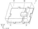
図11は、本実施形態に係るLEDパッケージを例示する斜視図であり、
図12は、本実施形態に係るLEDパッケージを例示する断面図である。Next, a third embodiment of the present invention will be described.
FIG. 11 is a perspective view illustrating an LED package according to this embodiment.
FIG. 12 is a cross-sectional view illustrating an LED package according to this embodiment.
図11及び図12に示すように、本実施形態に係るLEDパッケージ3においては、前述の第1の実施形態に係るLEDパッケージ1(図1参照)の構成に加えて、ツェナーダイオードチップ36等が設けられており、リードフレーム11とリードフレーム12との間に接続されている。すなわち、リードフレーム12の上面上に半田又は銀ペースト等の導電性材料からなるダイマウント材37が被着されており、その上にツェナーダイオードチップ36が設けられている。これにより、ツェナーダイオードチップ36がダイマウント材37を介してリードフレーム12上に搭載されると共に、ツェナーダイオードチップ36の下面端子(図示せず)が、ダイマウント材37を介してリードフレーム12に接続されている。また、ツェナーダイオードチップ36の上面端子36aは、ワイヤ38を介してリードフレーム11に接続されている。すなわち、ワイヤ38の一端はツェナーダイオードチップ36の上面端子36aに接続されており、ワイヤ38は上面端子36aから+Z方向に引き出され、−Z方向と−X方向との間の方向に向けて湾曲し、ワイヤ38の他端はリードフレーム11の上面に接合されている。 As shown in FIGS. 11 and 12, in the
これにより、本実施形態においては、ツェナーダイオードチップ36をLEDチップ14に対して並列に接続することができる。この結果、ESD(Electrostatic Discharge:静電気放電)に対する耐性が向上する。本実施形態における上記以外の構成、製造方法及び作用効果は、前述の第1の実施形態と同様である。 Thereby, in this embodiment, the
次に、本発明の第4の実施形態について説明する。
図13は、本実施形態に係るLEDパッケージを例示する斜視図であり、
図14は、本実施形態に係るLEDパッケージを例示する断面図である。Next, a fourth embodiment of the present invention will be described.
FIG. 13 is a perspective view illustrating an LED package according to this embodiment.
FIG. 14 is a cross-sectional view illustrating an LED package according to this embodiment.
図13及び図14に示すように、本実施形態に係るLEDパッケージ4は、前述の第3の実施形態に係るLEDパッケージ3(図11参照)と比較して、ツェナーダイオードチップ36がリードフレーム11に搭載されている点が異なっている。この場合、ツェナーダイオードチップ36の下面端子はダイマウント材37を介してリードフレーム11に接続されており、上面端子はワイヤ38を介してリードフレーム12に接続されている。本実施形態における上記以外の構成、製造方法及び作用効果は、前述の第3の実施形態と同様である。 As shown in FIGS. 13 and 14, the
次に、本発明の第5の実施形態について説明する。
図15は、本実施形態に係るLEDパッケージを例示する斜視図であり、
図16(a)は本実施形態に係るLEDパッケージを例示する平面図であり、(b)はその側面図である。
図15並びに図16(a)及び(b)に示すように、本実施形態に係るLEDパッケージ5は、前述の第1の実施形態に係るLEDパッケージ1(図1参照)と比較して、リードフレームの形状が異なっていると共に、LEDチップのタイプが異なっている。Next, a fifth embodiment of the present invention will be described.
FIG. 15 is a perspective view illustrating an LED package according to this embodiment.
FIG. 16A is a plan view illustrating an LED package according to this embodiment, and FIG. 16B is a side view thereof.
As shown in FIGS. 15 and 16 (a) and 16 (b), the
すなわち、LEDパッケージ5においては、一対のリードフレーム41及び42が設けられている。リードフレーム42はリードフレーム41よりも+X方向側に配置されている。また、リードフレーム42のX方向における長さは、リードフレーム41のX方向における長さよりも短い。 That is, the
リードフレーム41においては、ベース部41aから6本の吊ピン41b〜41gが延出している。吊ピン41b及び41cは、ベース部41aの+Y方向に向いた端縁の両端部付近から+Y方向に向けて延出しており、吊ピン41d及び41eは、ベース部41aの−X方向に向いた端縁の両端部から−X方向に向けて延出しており、吊ピン41f及び41gは、ベース部41aの−Y方向に向いた端縁の両端部付近から−Y方向に向けて延出している。また、ベース部41aの下面における+X方向側の端部を除く領域には、凸部41hが形成されている。一方、ベース部41aにおける凸部41hが形成されていない部分、すなわち、+X方向側の端部は、薄板部41tとなっている。更に、リードフレーム41における吊ピン41dと吊ピン41eとの間の領域には、+X方向に進入した切込41iが形成されている。切込41iは凸部41h内に進入しており、リードフレーム41をZ方向に貫通している。このため、下方(−Z方向)から見て、凸部41hの形状はコ字状である。すなわち、リードフレーム41における下面が透明樹脂体17から露出した部分に、Z方向に貫通した切込41iが形成されている。 In the
リードフレーム42においては、ベース部42aから、4本の吊ピン42b〜42eが延出している。吊ピン42bは、ベース部42aの+Y方向に向いた端縁全体から+Y方向に向けて延出しており、吊ピン42cは、ベース部42aの−Y方向に向いた端縁全体から−Y方向に向けて延出しており、吊ピン42d及び42eは、ベース部42aの+X方向に向いた端縁の両端部から+X方向に向けて延出している。また、ベース部41aの下面における−X方向側の端部には、凸部42hが形成されている。一方、ベース部42aにおける凸部42hが形成されていない部分、すなわち、−X方向側の端部は、薄板部42tとなっている。更に、リードフレーム42における吊ピン42dと吊ピン42eとの間の領域には、−X方向に進入した切込42iが形成されている。切込42iは凸部42h内に進入しており、リードフレーム42をZ方向に貫通している。このため、−Z方向から見て、凸部42hの形状はコ字状である。すなわち、リードフレーム42における下面が透明樹脂体17から露出した部分に、Z方向に貫通した切込42iが形成されている。 In the
X方向において、吊ピン41bの位置と吊ピン41gの位置とは相互に同一であり、吊ピン41cの位置と吊ピン41fの位置とは相互に同一であり、吊ピン42bの位置と吊ピン42cの位置とは相互に同一である。また、Y方向において、吊ピン41dの位置と吊ピン42eの位置とは相互に同一であり、吊ピン41eの位置と吊ピン42dの位置とは相互に同一であり、切込41iの位置と切込42iの位置とは相互に同一である。 In the X direction, the position of the hanging
リードフレーム41の上面41j上における吊ピン41bと吊ピン41gとの中間の領域には、導電性のダイマウント材43が設けられており、その上にはLEDチップ44が搭載されている。LEDチップ44は上下導通タイプのチップであり、その下面には下面端子(図示せず)が設けられており、その上面には上面端子44aが設けられている。LEDチップ44の下面端子は、ダイマウント材43を介してリードフレーム41に接続されている。一方、LEDチップ44の上面端子44aは、ワイヤ45を介して、リードフレーム42に接続されている。すなわち、ワイヤ45の一方の端部45aはLEDチップ44の上面端子44aに接合されており、他方の端部45bはリードフレーム42の上面42jにおける吊ピン42bと吊ピン42cとの中間の領域に接合されている。なお、ダイマウント材43は、例えば銀ペースト又は金属半田により形成されており、ワイヤ45は例えば金により形成されている。 A conductive
そして、ワイヤ45の端部45aは上面端子44aからほぼ水平方向(+X方向)に引き出されており、端部45bは上面42jからほぼ垂直方向(+Z方向)に引き出されている。すなわち、リードフレーム41の上面41j(XY平面)と上面端子44aからワイヤ45が引き出される方向(ほぼ+X方向)とのなす角度は、リードフレーム42の上面42j(XY平面)とリードフレーム42からワイヤ45が引き出される方向(ほぼ+Z方向)とのなす角度よりも小さい。本実施形態においては、ワイヤ45のボンディングに際して、先に端部45bをリードフレーム42の上面42jに接合し、その後、端部45aをLEDチップ44の上面端子44aに接合している。これにより、上述のような引出角度の大小関係が実現する。 The
本実施形態においても、前述の第1の実施形態と同様に、透明樹脂体17がリードフレーム41及び42、ダイマウント材43、LEDチップ44並びにワイヤ45を覆っており、透明樹脂体17の外形がLEDパッケージ5の外形となっている。そして、リードフレーム41の凸部41hの下面及びリードフレーム42の凸部42hの下面は、透明樹脂体17の下面における相互に離隔した領域において露出し、リードフレーム41及び42の各吊ピンの先端面は、透明樹脂体17の側面において露出している。また、透明樹脂体17は、切込41i及び42iの内部に進入している。 Also in the present embodiment, the
次に、本実施形態の作用効果について説明する。
図16(a)及び(b)に示すように、本実施形態に係るLEDパッケージ5は、実装基板120に実装されて使用される。実装に際しては、実装基板120の実装面121における相互に離隔した2ヶ所の矩形の領域に、半田フィレット125及び126を形成する。次に、LEDパッケージ5を実装面121上に載置する。このとき、リードフレーム41の凸部41hの下面を半田フィレット125に当接させ、リードフレーム42の凸部42hの下面を半田フィレット126に当接させる。そして、+Z方向から見て、切込41iを除く凸部41hの外縁を半田フィレット125の外縁と一致させ、切込42iを除く凸部42hの外縁を半田フィレット126の外縁と一致させる。次に、熱処理を行い、半田フィレット125及び126を一旦溶融させた後、凝固させる。これにより、リードフレーム41が半田フィレット125を介して実装基板120に接合されると共に、リードフレーム42が半田フィレット126を介して実装基板120に接合される。この結果、LEDパッケージ5が実装基板120に実装される。Next, the effect of this embodiment is demonstrated.
As shown in FIGS. 16A and 16B, the
そして、本実施形態においては、リードフレーム41に切込41iが形成されているため、透明樹脂体17及び切込41iを介して+Z方向から実装面121を観察することにより、LEDパッケージ5を実装面121に当接させた後でも半田フィレット125の有無を確認することができる。同様に、リードフレーム42には切込42iが形成されているため、透明樹脂体17及び切込42iを介して実装面121を+Z方向から観察することにより、LEDパッケージ5を実装面121に当接させた後でも半田フィレット126の有無を確認することができる。特に、透明樹脂体17は透明樹脂からなり、蛍光体を含有していないため、可視光の透過率が高く、観察が容易である。また、透明樹脂体17が切込41i及び42iの内部に進入することにより、リードフレーム41及び42と透明樹脂体17との密着性が良好になり、LEDパッケージ5の耐久性が向上する。 In the present embodiment, since the
更に、本実施形態においては、リードフレーム41及び42の上面から見て、上面端子44aからワイヤ45が引き出される角度を、リードフレーム42からワイヤ45が引き出される角度よりも小さくしている。これにより、ワイヤ45のループの高さを抑え、LEDパッケージ5全体の厚さを薄くすることができる。更にまた、上下導通タイプのLEDチップ44を採用し、ワイヤの本数を1本とすることにより、ワイヤ同士の接触を確実に防止すると共に、ワイヤボンディング工程を簡略化することができる。本実施形態における上記以外の構成、製造方法及び作用効果は、前述の第1の実施形態と同様である。 Further, in the present embodiment, the angle at which the
なお、本実施形態においては、リードフレーム41及び42にそれぞれ切込41i及び42iを形成する例を示したが、各リードフレームの内部に、Z方向に貫通した窓を形成してもよい。これにより、窓を介して半田フィレットの有無を確認できると共に、透明樹脂体17との密着性が良好になる。 In the present embodiment, an example in which the
次に、本発明の第6の実施形態について説明する。
図17は、本実施形態に係るLEDパッケージを例示する斜視図である。
図17に示すように、本実施形態に係るLEDパッケージ6は、前述の第5の実施形態に係るLEDパッケージ5(図15参照)と比較して、LEDチップが搭載されたリードフレームの形状が異なっている。Next, a sixth embodiment of the present invention will be described.
FIG. 17 is a perspective view illustrating an LED package according to this embodiment.
As shown in FIG. 17, the
すなわち、本実施形態に係るLEDパッケージ6においては、リードフレーム41(図15参照)の代わりに、リードフレーム51が設けられている。リードフレーム51においては、その上面51jにおけるベース部51aのX方向中央部に相当する領域が、それ以外の領域に対して凹んでいる。すなわち、リードフレーム51の上面51jにおけるX方向中央部には、凹部51kが形成されている。そして、この凹部51k内にLEDチップ44が配置されている。 That is, in the
本実施形態によれば、リードフレーム51に凹部51kを形成し、その内部にLEDチップ44を配置することにより、LEDパッケージのより一層の低背化を図ることができる。本実施形態における上記以外の構成、製造方法及び作用効果は、前述の第5の実施形態と同様である。 According to the present embodiment, the
次に、本発明の第7の実施形態について説明する。
図18は、本実施形態に係るLEDパッケージを例示する斜視図であり、
図19(a)は本実施形態に係るLEDパッケージを例示する平面図であり、(b)はその側面図である。
図18並びに図19(a)及び(b)に示すように、本実施形態に係るLEDパッケージ7は、前述の第5の実施形態に係るLEDパッケージ5(図15参照)と比較して、LEDチップが搭載されたリードフレームの形状が異なっている。Next, a seventh embodiment of the present invention will be described.
FIG. 18 is a perspective view illustrating an LED package according to this embodiment.
FIG. 19A is a plan view illustrating an LED package according to this embodiment, and FIG. 19B is a side view thereof.
As shown in FIGS. 18 and 19 (a) and 19 (b), the
すなわち、本実施形態に係るLEDパッケージ7においては、LEDチップ44が搭載されたリードフレーム61のX方向における長さが、前述の第5の実施形態におけるリードフレーム41(図15参照)よりも長く、リードフレーム61の下面にはX方向において離隔した2つの凸部61m及び61nが形成されている。凸部61mは凸部61nよりも−X方向側に位置している。また、LEDチップ44が搭載されていないリードフレーム62のX方向における長さも、前述の第6の実施形態におけるリードフレーム42よりも長い。但し、リードフレーム62の下面に形成された凸部62hは1つである。 That is, in the
また、リードフレーム61における吊ピン61dと吊ピン61eとの間の領域には、+X方向に進入した切込61iが形成されている。−Z方向から見て、切込61iの先端は凸部61mの内部に位置している。同様に、リードフレーム62における吊ピン62dと吊ピン62eとの間の領域には、−X方向に進入した切込62iが形成されている。−Z方向から見て、切込62iの先端は凸部62hの内部に位置している。このため、下方(−Z方向)から見て、凸部61m及び凸部62hの形状は共にコ字状である。凸部61mの形状及びサイズは、凸部62hの形状及びサイズと同一であり、YZ平面に関して対称である。凸部61m及び62hは、LEDパッケージ7の外部電極パッドとして機能する。 Further, in the region between the
本実施形態においては、外部電極パッドとして使用する凸部61mの下面及び凸部62hの下面の形状及びサイズが相互に同一である。このため、LEDパッケージ7を実装基板120に実装する際に、半田フィレット125の形状及びサイズを、半田フィレット126の形状及びサイズと同一にすることができる。これにより、前述のマンハッタン現象を防止することができる。また、前述の第5の実施形態と同様に、LEDパッケージ7を実装基板120に実装する際に、切込61i及び62iを介して半田フィラー125及び126の有無を確認することができる。更に、切込61i及び62i内に透明樹脂体17が進入するため、リードフレーム61及び62と透明樹脂体17との密着性が良好である。本実施形態における上記以外の構成、製造方法及び作用効果は、前述の第5の実施形態と同様である。 In the present embodiment, the shape and size of the lower surface of the
次に、本発明の第8の実施形態について説明する。
図20は、本実施形態に係るLEDパッケージを例示する斜視図であり、
図21は、本実施形態に係るLEDパッケージを例示する断面図である。Next, an eighth embodiment of the present invention will be described.
FIG. 20 is a perspective view illustrating an LED package according to this embodiment.
FIG. 21 is a cross-sectional view illustrating an LED package according to this embodiment.
図20及び図21に示すように、本実施形態に係るLEDパッケージ8は、前述の第1の実施形態に係るLEDパッケージ1(図1参照)と比較して、上面端子型のLEDチップ14の代わりに、フリップタイプのLEDチップ66が設けられている点が異なっている。すなわち、本実施形態に係るLEDパッケージ8においては、LEDチップ66の下面に2つの端子が設けられている。また、LEDチップ66はリードフレーム11とリードフレーム12とを跨ぐようにブリッジ状に配置されている。LEDチップ66の一方の下面端子はリードフレーム11に接続されており、他方の下面端子はリードフレーム12に接続されている。 As shown in FIGS. 20 and 21, the
本実施形態においては、フリップタイプのLEDチップ66を採用してワイヤをなくすことにより、上方への光の取出効率を高めると共に、ワイヤボンディング工程を省略することができる。また、LEDパッケージのより一層の低背化を図ることができる。更に、透明樹脂体17の熱応力に起因してワイヤが破断することも防止できる。本実施形態における上記以外の構成、製造方法及び作用効果は、前述の第1の実施形態と同様である。 In the present embodiment, by adopting the flip
次に、本発明の第9の実施形態について説明する。
図22は、本実施形態に係るLEDパッケージを例示する斜視図である。
図22に示すように、本実施形態は、前述の第1の実施形態と第5の実施形態とを組み合わせた例である。すなわち、本実施形態に係るLEDパッケージ9においては、前述の第1の実施形態(図1参照)において説明したリードフレーム11及び12が設けられている。そして、このリードフレーム11上に、前述の第5の実施形態(図15参照)において説明した上下導通タイプのLEDチップ44が搭載されている。LEDチップ44の下面端子はダイマウント材43を介してリードフレーム11に接続されており、LEDチップ44の上面端子44aはワイヤ45を介してリードフレーム12に接続されている。Next, a ninth embodiment of the present invention will be described.
FIG. 22 is a perspective view illustrating an LED package according to this embodiment.
As shown in FIG. 22, the present embodiment is an example in which the first embodiment and the fifth embodiment described above are combined. That is, the
そして、前述の第5の実施形態と同様に、ワイヤ45の端部45aは上面端子44aからほぼ水平方向(+X方向)に引き出されており、端部45bはリードフレーム12の上面からほぼ垂直方向(+Z方向)に引き出されている。すなわち、リードフレーム11の上面(XY平面)と上面端子44aからワイヤ45が引き出される方向(ほぼ+X方向)とのなす角度は、リードフレーム12の上面(XY平面)とリードフレーム12からワイヤ45が引き出される方向(ほぼ+Z方向)とのなす角度よりも小さい。 As in the fifth embodiment described above, the
本実施形態においても、前述の第5の実施形態と同様に、ワイヤ45のループの高さを抑え、LEDパッケージ9全体の厚さを薄くすることができる。また、上下導通タイプのLEDチップ44を採用し、ワイヤの本数を1本とすることにより、ワイヤ同士の接触を確実に防止すると共に、ワイヤボンディング工程を簡略化することができる。本実施形態における上記以外の構成、製造方法及び作用効果は、前述の第1の実施形態と同様である。 Also in this embodiment, like the above-described fifth embodiment, the height of the loop of the
次に、本発明の第10の実施形態について説明する。
図23は、本実施形態に係るLEDパッケージを例示する断面図である。
図23に示すように、本実施形態に係るLEDパッケージ10においては、前述の第5の実施形態に係るLEDパッケージ5(図15参照)の構成に加えて、透明樹脂体17上にレンズ71が設けられている。レンズ71は、透明樹脂からなり、凸面が上方に向いた平凸レンズである。レンズ71は、例えば下金型101(図5参照)の底面に凹部を形成することにより透明樹脂体17と一体的に形成してもよく、透明樹脂板29(図6参照)を形成後に透明樹脂板29に取り付けて、その後、透明樹脂板29をダイシングしてもよく、透明樹脂板29をダイシングした後に透明樹脂体17に取り付けてもよい。本実施形態によれば、透明樹脂体17から出射した光をレンズ71によって直上方向(+Z方向)に集光させることができるため、配向性が向上する。本実施形態における上記以外の構成、製造方法及び作用効果は、前述の第5の実施形態と同様である。Next, a tenth embodiment of the present invention will be described.
FIG. 23 is a cross-sectional view illustrating an LED package according to this embodiment.
As shown in FIG. 23, in the
以上、本発明のいくつかの実施形態を説明したが、これらの実施形態は、例として提示したものであり、発明の範囲を限定することは意図していない。これら新規な実施形態は、その他の様々な形態で実施されることが可能であり、発明の要旨を逸脱しない範囲で、種々の省略、置き換え、変更を行うことができる。これら実施形態やその変形は、発明の範囲や要旨に含まれるとともに、特許請求の範囲に記載された発明及びその等価物の範囲に含まれる。また、前述の各実施形態は、相互に組み合わせて実施することができる。 As mentioned above, although some embodiment of this invention was described, these embodiment is shown as an example and is not intending limiting the range of invention. These novel embodiments can be implemented in various other forms, and various omissions, replacements, and changes can be made without departing from the scope of the invention. These embodiments and modifications thereof are included in the scope and gist of the invention, and are included in the scope of the invention described in the claims and the equivalents thereof. Further, the above-described embodiments can be implemented in combination with each other.
例えば、前述の第1の実施形態においては、リードフレームシート23をウェットエッチングによって形成する例を示したが、本発明はこれに限定されず、例えばプレス等の機械的な手段によって形成してもよい。また、前述の各実施形態においては、1つのLEDパッケージに1個のLEDチップを搭載する例を示したが、本発明はこれに限定されず、1つのLEDパッケージに複数個のLEDチップを搭載してもよい。更に、リードフレームの上面におけるダイマウント材を形成する予定の領域とワイヤを接合する予定の領域との間に、溝を形成してもよい。又は、リードフレームの上面におけるダイマウント材を形成する予定の領域に凹部を形成してもよい。これにより、ダイマウント材の供給量又は供給位置がばらついても、ダイマウント材がワイヤの接合予定領域まで流出することを防止でき、ワイヤの接合が阻害されることを防止できる。更にまた、透明樹脂体17には蛍光体を含有させてもよい。 For example, in the above-described first embodiment, the example in which the
更にまた、前述の第1の実施形態においては、リードフレームにおいて、銅板の上下面上に銀めっき層が形成されている例を示したが、本発明はこれに限定されない。例えば、銅板の上下面上に銀めっき層が形成され、少なくとも一方の銀めっき層上にロジウム(Rh)めっき層が形成されていてもよい。また、銅板と銀めっき層との間に銅(Cu)めっき層が形成されていてもよい。更に、銅板の上下面上にニッケル(Ni)めっき層が形成されており、ニッケルめっき層上に金と銀との合金(Au−Ag合金)めっき層が形成されていてもよい。 Furthermore, in the above-described first embodiment, the example in which the silver plating layers are formed on the upper and lower surfaces of the copper plate in the lead frame has been shown, but the present invention is not limited to this. For example, a silver plating layer may be formed on the upper and lower surfaces of the copper plate, and a rhodium (Rh) plating layer may be formed on at least one of the silver plating layers. Further, a copper (Cu) plating layer may be formed between the copper plate and the silver plating layer. Furthermore, a nickel (Ni) plating layer may be formed on the upper and lower surfaces of the copper plate, and an alloy (Au—Ag alloy) plating layer of gold and silver may be formed on the nickel plating layer.
更にまた、前述の各実施形態及びその変形例においては、リードフレームのベース部の形状が上方から見て矩形である例を示したが、ベース部の形状は少なくとも1つの角部が落とされた形状であってもよい。これにより、LEDパッケージの角部近傍において、直角又は鋭角の角部が除去されるため、これらの角部が樹脂剥がれやクラックの基点となることがない。この結果、LEDパッケージ全体として、樹脂剥がれ及びクラックの発生を抑制することができる。 Furthermore, in each of the above-described embodiments and modifications thereof, an example was shown in which the shape of the base portion of the lead frame was a rectangle when viewed from above, but the shape of the base portion was dropped at least one corner. It may be a shape. As a result, right-angle or acute-angle corners are removed in the vicinity of the corners of the LED package, so that these corners do not become a base point for resin peeling or cracking. As a result, the resin package and the occurrence of cracks can be suppressed as the entire LED package.
以上説明した実施形態によれば、耐久性が高く、コストが低いLEDパッケージ及びその製造方法を実現することができる。 According to the embodiment described above, an LED package with high durability and low cost and a manufacturing method thereof can be realized.
1、2、3、4、5、6、7、8、9、10 LEDパッケージ、11 リードフレーム、11a ベース部、11b〜11e 吊ピン、11f 下面、11g 凸部、11h 上面、11t 薄板部、12 リードフレーム、12a ベース部、12b〜12e 吊ピン、12f 下面、12g 凸部、12h 上面、12t 薄板部、13 ダイマウント材、14 LEDチップ、14a、14b 端子、15、16 ワイヤ、17 透明樹脂体、17a〜17d 側面、21 導電シート、21a 銅板、21b 銀めっき層、22a、22b マスク、22c 開口部、23 リードフレームシート、23a 開口部、23b、23c ブリッジ、24 補強テープ、26 樹脂材料、29 透明樹脂板、31 リードフレーム、31d、31e 吊ピン、31g 凸部、32 リードフレーム、32b、32c 吊ピン、32g 凸部、36 ツェナーダイオードチップ、36a 上面端子、37 ダイマウント材、38 ワイヤ、41 リードフレーム、41a ベース部、41b〜41g 吊ピン、41h 凸部、41i 切込、41j 上面、41t 薄板部、42 リードフレーム、42a ベース部、42b〜42e 吊ピン、42h 凸部、42i 切込、42j 上面、42t 薄板部、43 ダイマウント材、44 LEDチップ、44a 上面端子、45 ワイヤ、45a、45b 端部、51 リードフレーム、51a ベース部、51j 上面、51k 凹部、61 リードフレーム、61a ベース部、61b〜61g 吊ピン、61i 切込、61m、61n 凸部、61t 薄板部、62 リードフレーム、62a ベース部、62b〜62e 吊ピン、62h 凸部、62i 切込、62t 薄板部、66 LEDチップ、71 レンズ、101 下金型、101a 凹部、102 上金型、103 ディスペンサ、104 ブレード、111 レジスト膜、111a レジストマスク、112 マスクパターン、113 マスク、120 実装基板、121 実装面、125、126 半田フィレット、B ブロック、D ダイシング領域、P 素子領域1, 2, 3, 4, 5, 6, 7, 8, 9, 10 LED package, 11 lead frame, 11a base portion, 11b to 11e hanging pin, 11f lower surface, 11g convex portion, 11h upper surface, 11t thin plate portion, 12 Lead frame, 12a Base part, 12b-12e Hanging pin, 12f Lower surface, 12g Convex part, 12h Upper surface, 12t Thin plate part, 13 Die mount material, 14 LED chip, 14a, 14b Terminal, 15, 16 Wire, 17 Transparent resin Body, 17a-17d side, 21 conductive sheet, 21a copper plate, 21b silver plating layer, 22a, 22b mask, 22c opening, 23 lead frame sheet, 23a opening, 23b, 23c bridge, 24 reinforcing tape, 26 resin material, 29 Transparent resin plate, 31 Lead frame, 31d, 31e Hanging pin, 1g Convex part, 32 Lead frame, 32b, 32c Suspension pin, 32g Convex part, 36 Zener diode chip, 36a Top surface terminal, 37 Die mount material, 38 Wire, 41 Lead frame, 41a Base part, 41b-41g Suspension pin, 41h Convex part, 41i notch, 41j top surface, 41t thin plate part, 42 lead frame, 42a base part, 42b to 42e Hanging pin, 42h Convex part, 42i notch, 42j top surface, 42t thin plate part, 43 Die mount material, 44 LED Chip, 44a top surface terminal, 45 wire, 45a, 45b end, 51 lead frame, 51a base portion, 51j top surface, 51k recess, 61 lead frame, 61a base portion, 61b-61g hanging pin, 61i notch, 61m, 61n Projection, 61t Thin plate, 62 Frame, 62a base part, 62b to 62e hanging pin, 62h convex part, 62i notch, 62t thin plate part, 66 LED chip, 71 lens, 101 lower mold, 101a concave part, 102 upper mold, 103 dispenser, 104 blade , 111 resist film, 111a resist mask, 112 mask pattern, 113 mask, 120 mounting substrate, 121 mounting surface, 125, 126 solder fillet, B block, D dicing area, P element area
Claims (9)
Translated fromJapanese前記第1及び第2のリードフレームの上方に設けられ、少なくともインジウム、ガリウム及びアルミニウムを含有する半導体層を有し、一方の端子が前記第1のリードフレームに接続され、他方の端子が前記第2のリードフレームに接続されたLEDチップと、
前記第1及び第2のリードフレームのそれぞれの上面全体、下面の一部及び端面の一部を覆い、前記LEDチップを覆い、前記下面の残部及び前記端面の残部を露出させた透明な樹脂体と、
を備え、
前記第1のリードフレームにおける下面が前記樹脂体から露出した部分には、上下方向に貫通した第1の切込が形成されており、
前記第2のリードフレームにおける下面が前記樹脂体から露出した部分には、上下方向に貫通した第2の切込が形成されており、
前記樹脂体の外形がその外形をなし、
前記第1のリードフレームの下面及び前記第2のリードフレームの下面にはそれぞれ凸部が形成されており、
前記凸部の下面は前記樹脂体の下面において露出し、前記凸部の側面は前記樹脂体によって覆われ、
前記第1の切込は、前記第1のリードフレームに形成された前記凸部内に進入しており、前記第1のリードフレームの前記凸部の下面の形状はコ字形状であり、
前記第2の切込は、前記第2のリードフレームに形成された前記凸部内に進入しており、前記第2のリードフレームの前記凸部の下面の形状はコ字形状であり、
前記第1のリードフレーム及び前記第2のリードフレームは、それぞれ、
端面が前記樹脂体によって覆われたベース部と、
前記ベース部から相互に異なる方向に延出し、その下面が前記樹脂体によって覆われ、その先端面が前記樹脂体の側面に露出した複数本の吊ピンと、
を有し、
前記第1のリードフレームの前記複数本の吊ピンのうちの2本は、前記第1のリードフレームの前記ベース部における前記第2のリードフレームの反対側の端面から延出しており、
前記第1の切込は、前記第1のリードフレームの前記2本の吊ピンの間に位置しており、
前記第2のリードフレームの前記複数本の吊ピンのうちの2本は、前記第2のリードフレームの前記ベース部における前記第1のリードフレームの反対側の端面から延出しており、
前記第2の切込は、前記第2のリードフレームの前記2本の吊ピンの間に位置していることを特徴とするLEDパッケージ。First and second lead frames spaced apart from each other;
Provided above the first and second lead frames, and having a semiconductor layer containing at least indium, gallium and aluminum, one terminal connected to the first lead frame, and the other terminal being the first LED chips connected to two lead frames;
A transparent resin body that covers the entire upper surface, part of the lower surface, and part of the end surface of each of the first and second lead frames, covers the LED chip, and exposes the remaining part of the lower surface and the remaining part of the end surface. When,
With
In the portion where the lower surface of the first lead frame is exposed from the resin body, a first notch penetrating in the vertical direction is formed,
In the portion where the lower surface of the second lead frame is exposed from the resin body, a second notch penetrating in the vertical direction is formed,
It outer shape of the resin body name itscontour,
Convex portions are formed on the lower surface of the first lead frame and the lower surface of the second lead frame,
The lower surface of the convex portion is exposed on the lower surface of the resin body, and the side surface of the convex portion is covered with the resin body,
The first notch has entered into the convex portion formed in the first lead frame, and the shape of the lower surface of the convex portion of the first lead frame is a U-shape,
The second notch has entered the convex portion formed in the second lead frame, and the shape of the bottom surface of the convex portion of the second lead frame is a U-shape,
The first lead frame and the second lead frame are respectively
A base portion whose end face is covered with the resin body;
A plurality of suspension pins extending from the base portion in different directions, the lower surface of which is covered with the resin body, and the tip surface of which is exposed on the side surface of the resin body;
Have
Two of the plurality of extending pins of the first lead frame extend from an end surface of the base portion of the first lead frame opposite to the second lead frame,
The first notch is located between the two suspension pins of the first lead frame;
Two of the plurality of extending pins of the second lead frame extend from an end surface of the base portion of the second lead frame opposite to the first lead frame,
The LED package, wherein the second notch is located between the two extending pins of the second lead frame.
前記一方の端子は前記LEDチップの下面に設けられており、前記他方の端子は前記LEDチップの上面に設けられており、
導電性材料からなり、前記LEDチップを前記第1のリードフレームに固着させると共に、前記一方の端子を前記第1のリードフレームに接続するダイマウント材と、
前記他方の端子を前記第2のリードフレームに接続するワイヤと、
をさらに備えたことを特徴とする請求項1〜4のいずれか1つに記載のLEDパッケージ。The LED chip is mounted on the first lead frame;
The one terminal is provided on the lower surface of the LED chip, and the other terminal is provided on the upper surface of the LED chip,
A die mount material made of a conductive material, fixing the LED chip to the first lead frame, and connecting the one terminal to the first lead frame;
A wire connecting the other terminal to the second lead frame;
The LED package according to claim 1, further comprising:
端面が前記樹脂体によって覆われたベース部と、
前記ベース部から相互に異なる方向に延出し、その下面が前記樹脂体によって覆われ、その先端面が前記樹脂体の側面に露出した複数本の吊ピンと、
を有することを特徴とする請求項1〜7のいずれか1つに記載のLEDパッケージ。At least one of the first lead frame and the second lead frame is:
A base portion whose end face is covered with the resin body;
A plurality of suspension pins extending from the base portion in different directions, the lower surface of which is covered with the resin body, and the tip surface of which is exposed on the side surface of the resin body;
The LED package according to anyone of claims1 to7 , characterized by comprising:
前記第1のリードフレーム及び前記第2のリードフレームのうちの少なくとも一方は、
端面が前記樹脂体によって覆われたベース部と、
前記ベース部から延出し、その下面が前記樹脂体によって覆われ、その先端面が前記樹脂体の3つの側面に露出した複数本の吊ピンと、
を有することを特徴とする請求項1〜7のいずれか1つに記載のLEDパッケージ。When viewed from above, the shape of the resin body is rectangular,
At least one of the first lead frame and the second lead frame is:
A base portion whose end face is covered with the resin body;
A plurality of suspension pins extending from the base portion, the lower surface of which is covered with the resin body, and the tip surfaces of which are exposed on the three side surfaces of the resin body;
The LED package according to anyone of claims1 to7 , characterized by comprising:
Priority Applications (4)
| Application Number | Priority Date | Filing Date | Title |
|---|---|---|---|
| JP2010186505AJP5383611B2 (en) | 2010-01-29 | 2010-08-23 | LED package |
| US12/886,890US8637892B2 (en) | 2010-01-29 | 2010-09-21 | LED package and method for manufacturing same |
| TW100101959ATWI446596B (en) | 2010-01-29 | 2011-01-19 | Led package and method for manufacturing same |
| CN201110032319.9ACN102142513B (en) | 2010-01-29 | 2011-01-26 | LED package and method for manufacturing same |
Applications Claiming Priority (3)
| Application Number | Priority Date | Filing Date | Title |
|---|---|---|---|
| JP2010019782 | 2010-01-29 | ||
| JP2010019782 | 2010-01-29 | ||
| JP2010186505AJP5383611B2 (en) | 2010-01-29 | 2010-08-23 | LED package |
Publications (3)
| Publication Number | Publication Date |
|---|---|
| JP2011176271A JP2011176271A (en) | 2011-09-08 |
| JP2011176271A5 JP2011176271A5 (en) | 2012-10-11 |
| JP5383611B2true JP5383611B2 (en) | 2014-01-08 |
Family
ID=44340853
Family Applications (1)
| Application Number | Title | Priority Date | Filing Date |
|---|---|---|---|
| JP2010186505AActiveJP5383611B2 (en) | 2010-01-29 | 2010-08-23 | LED package |
Country Status (4)
| Country | Link |
|---|---|
| US (1) | US8637892B2 (en) |
| JP (1) | JP5383611B2 (en) |
| CN (1) | CN102142513B (en) |
| TW (1) | TWI446596B (en) |
Families Citing this family (34)
| Publication number | Priority date | Publication date | Assignee | Title |
|---|---|---|---|---|
| JP2010512662A (en) | 2006-12-11 | 2010-04-22 | ザ リージェンツ オブ ザ ユニバーシティ オブ カリフォルニア | Transparent light emitting diode |
| TWI365525B (en)* | 2007-12-24 | 2012-06-01 | Ind Tech Res Inst | An ultra thin package for a sensor chip of a micro electro mechanical system |
| JP5464825B2 (en)* | 2008-07-23 | 2014-04-09 | ローム株式会社 | LED module |
| JP5217800B2 (en) | 2008-09-03 | 2013-06-19 | 日亜化学工業株式会社 | Light emitting device, resin package, resin molded body, and manufacturing method thereof |
| KR101034054B1 (en)* | 2009-10-22 | 2011-05-12 | 엘지이노텍 주식회사 | Light emitting device package and manufacturing method thereof |
| CN102222625A (en)* | 2010-04-16 | 2011-10-19 | 展晶科技(深圳)有限公司 | Manufacturing method of light-emitting diode (LED) packaging structure and base thereof |
| JP5528900B2 (en)* | 2010-04-30 | 2014-06-25 | ローム株式会社 | Light emitting element module |
| MY170920A (en) | 2010-11-02 | 2019-09-17 | Carsem M Sdn Bhd | Leadframe package with recessed cavity for led |
| EP2639841B1 (en) | 2010-11-11 | 2019-07-24 | Nichia Corporation | Light-emitting device, and method for manufacturing circuit board |
| TWD145643S (en)* | 2011-04-28 | 2012-03-01 | 東芝股份有限公司 | Light-emitting diode |
| USD656469S1 (en)* | 2011-04-28 | 2012-03-27 | Kabushiki Kaisha Toshiba | Portion of a light-emitting diode |
| MY156107A (en)* | 2011-11-01 | 2016-01-15 | Carsem M Sdn Bhd | Large panel leadframe |
| US9093621B2 (en)* | 2011-12-28 | 2015-07-28 | Nichia Corporation | Molded package for light emitting device |
| CN103205692A (en)* | 2012-01-16 | 2013-07-17 | 昆山允升吉光电科技有限公司 | A machining process and a rework process for a mask plate for vapor deposition |
| KR101908656B1 (en)* | 2012-04-09 | 2018-10-16 | 엘지이노텍 주식회사 | A light emitting device package |
| CN103887410B (en)* | 2012-12-21 | 2017-02-01 | 展晶科技(深圳)有限公司 | Manufacturing method of light-emitting diode |
| US9166131B2 (en)* | 2013-07-17 | 2015-10-20 | Tai-Yin Huang | Composite LED package and its application to light tubes |
| JP2015095486A (en)* | 2013-11-08 | 2015-05-18 | アイシン精機株式会社 | Semiconductor device |
| TW201543720A (en)* | 2014-05-06 | 2015-11-16 | Genesis Photonics Inc | Package structure and preparation method thereof |
| DE102014119390A1 (en)* | 2014-12-22 | 2016-06-23 | Osram Opto Semiconductors Gmbh | Optoelectronic component and method for its production |
| JP6573356B2 (en)* | 2015-01-22 | 2019-09-11 | 大口マテリアル株式会社 | Lead frame |
| US11195269B2 (en)* | 2015-03-27 | 2021-12-07 | Texas Instruments Incorporated | Exposed pad integrated circuit package |
| JP6896038B2 (en)* | 2015-05-12 | 2021-06-30 | 三菱電機株式会社 | Display device |
| CN106571383B (en) | 2015-10-08 | 2020-04-28 | 联华电子股份有限公司 | Semiconductor element and manufacturing method thereof |
| TWI590433B (en) | 2015-10-12 | 2017-07-01 | 財團法人工業技術研究院 | Light-emitting element and display method |
| US10461233B2 (en) | 2015-11-27 | 2019-10-29 | Lg Innotek Co., Ltd. | Light emitting device package and lighting device |
| TWI634679B (en)* | 2017-03-27 | 2018-09-01 | 隆達電子股份有限公司 | Light-emitting diode device and its bracket |
| JP6977338B2 (en)* | 2017-07-03 | 2021-12-08 | 大日本印刷株式会社 | LED module |
| KR102641336B1 (en) | 2017-09-05 | 2024-02-28 | 쑤저우 레킨 세미컨덕터 컴퍼니 리미티드 | Semiconductor device package |
| US10998256B2 (en)* | 2018-12-31 | 2021-05-04 | Texas Instruments Incorporated | High voltage semiconductor device lead frame and method of fabrication |
| CN112864296B (en)* | 2019-01-29 | 2022-06-28 | 泉州三安半导体科技有限公司 | An LED package device |
| CN110649145A (en)* | 2019-09-25 | 2020-01-03 | 广东晶科电子股份有限公司 | A kind of etched sheet frame, package bracket and LED device |
| US11592166B2 (en) | 2020-05-12 | 2023-02-28 | Feit Electric Company, Inc. | Light emitting device having improved illumination and manufacturing flexibility |
| US11876042B2 (en) | 2020-08-03 | 2024-01-16 | Feit Electric Company, Inc. | Omnidirectional flexible light emitting device |
Family Cites Families (35)
| Publication number | Priority date | Publication date | Assignee | Title |
|---|---|---|---|---|
| US5798536A (en)* | 1996-01-25 | 1998-08-25 | Rohm Co., Ltd. | Light-emitting semiconductor device and method for manufacturing the same |
| DE19638667C2 (en)* | 1996-09-20 | 2001-05-17 | Osram Opto Semiconductors Gmbh | Mixed-color light-emitting semiconductor component with luminescence conversion element |
| US6335548B1 (en)* | 1999-03-15 | 2002-01-01 | Gentex Corporation | Semiconductor radiation emitter package |
| JP2001326295A (en) | 2000-05-15 | 2001-11-22 | Rohm Co Ltd | Semiconductor device and semiconductor device manufacturing frame |
| DE10131698A1 (en)* | 2001-06-29 | 2003-01-30 | Osram Opto Semiconductors Gmbh | Surface-mountable radiation-emitting component and method for its production |
| JP2003110145A (en) | 2001-09-27 | 2003-04-11 | Harvatek Corp | Airfoil surface mount package for light emitting diodes |
| JP2003110080A (en) | 2001-09-28 | 2003-04-11 | Citizen Electronics Co Ltd | Semiconductor device |
| DE10392365T5 (en)* | 2002-03-08 | 2005-04-21 | Rohm Co. Ltd. | Semiconductor device with a semiconductor chip |
| US6830496B2 (en)* | 2003-01-22 | 2004-12-14 | Kaylu Industrial Corporation | Method of fabricating light emitting diode device with multiple encapsulants |
| JP4522049B2 (en) | 2003-02-14 | 2010-08-11 | 三洋電機株式会社 | Semiconductor device |
| JP3910171B2 (en) | 2003-02-18 | 2007-04-25 | シャープ株式会社 | Semiconductor light emitting device, method for manufacturing the same, and electronic imaging device |
| US20040227151A1 (en)* | 2003-03-31 | 2004-11-18 | Hitachi Cable, Ltd. | Light emitting diode |
| TWI275189B (en)* | 2003-12-30 | 2007-03-01 | Osram Opto Semiconductors Gmbh | Radiation-emitting and/or radiation-receiving semiconductor component and method for producing such component |
| JP2006093672A (en) | 2004-08-26 | 2006-04-06 | Toshiba Corp | Semiconductor light emitting device |
| JP3999780B2 (en) | 2004-11-16 | 2007-10-31 | 日電精密工業株式会社 | Lead frame manufacturing method |
| JP2007027281A (en) | 2005-07-13 | 2007-02-01 | Toshiba Corp | Semiconductor device |
| US8044418B2 (en)* | 2006-07-13 | 2011-10-25 | Cree, Inc. | Leadframe-based packages for solid state light emitting devices |
| JP4865525B2 (en)* | 2006-08-03 | 2012-02-01 | イッツウェル カンパニー リミテッド | SML type light emitting diode lamp element and manufacturing method thereof |
| JP4306772B2 (en) | 2006-10-05 | 2009-08-05 | 日亜化学工業株式会社 | Light emitting device |
| JP5232394B2 (en) | 2007-02-28 | 2013-07-10 | ローム株式会社 | Manufacturing method of semiconductor device |
| WO2008153043A1 (en)* | 2007-06-14 | 2008-12-18 | Rohm Co., Ltd. | Semiconductor light emitting device |
| TWI455672B (en) | 2007-07-06 | 2014-10-01 | Murata Manufacturing Co | A method for forming a hole for connecting a conductor for a layer, a method for manufacturing a resin substrate and a component-mounted substrate, and a method of manufacturing a resin substrate and a component |
| KR100998233B1 (en)* | 2007-12-03 | 2010-12-07 | 서울반도체 주식회사 | Slim LED Package |
| CN101939852A (en)* | 2007-12-24 | 2011-01-05 | 三星Led株式会社 | LED Package |
| US20100327044A1 (en) | 2008-02-25 | 2010-12-30 | Panasonic Corporation | Method for manufacturing electronic component module |
| JP4951090B2 (en) | 2010-01-29 | 2012-06-13 | 株式会社東芝 | LED package |
| JP5010693B2 (en) | 2010-01-29 | 2012-08-29 | 株式会社東芝 | LED package |
| JP5010716B2 (en) | 2010-01-29 | 2012-08-29 | 株式会社東芝 | LED package |
| JP2011159767A (en) | 2010-01-29 | 2011-08-18 | Toshiba Corp | Led package and method for manufacturing the same |
| MY155671A (en) | 2010-01-29 | 2015-11-13 | Toshiba Kk | LED package and method for manufacturing same |
| JP2011165833A (en) | 2010-02-08 | 2011-08-25 | Toshiba Corp | Led module |
| JP2011253910A (en)* | 2010-06-01 | 2011-12-15 | Toshiba Corp | Light-emitting device |
| JP2012113919A (en)* | 2010-11-24 | 2012-06-14 | Toshiba Corp | Lighting device |
| JP2012114286A (en)* | 2010-11-25 | 2012-06-14 | Toshiba Corp | Led package |
| JP2012234955A (en)* | 2011-04-28 | 2012-11-29 | Toshiba Corp | Led package and method for manufacturing the same |
- 2010
- 2010-08-23JPJP2010186505Apatent/JP5383611B2/enactiveActive
- 2010-09-21USUS12/886,890patent/US8637892B2/enactiveActive
- 2011
- 2011-01-19TWTW100101959Apatent/TWI446596B/enactive
- 2011-01-26CNCN201110032319.9Apatent/CN102142513B/enactiveActive
Also Published As
| Publication number | Publication date |
|---|---|
| US20110186902A1 (en) | 2011-08-04 |
| CN102142513A (en) | 2011-08-03 |
| TWI446596B (en) | 2014-07-21 |
| JP2011176271A (en) | 2011-09-08 |
| CN102142513B (en) | 2014-07-16 |
| TW201145616A (en) | 2011-12-16 |
| US8637892B2 (en) | 2014-01-28 |
Similar Documents
| Publication | Publication Date | Title |
|---|---|---|
| JP5383611B2 (en) | LED package | |
| JP5010693B2 (en) | LED package | |
| JP5010716B2 (en) | LED package | |
| US8338845B2 (en) | LED package and method for manufacturing the same | |
| JP4951090B2 (en) | LED package | |
| JP4886886B2 (en) | LED package manufacturing method | |
| JP4764519B1 (en) | LED package | |
| US20120273826A1 (en) | Led package and method for manufacturing same | |
| JP2011253882A (en) | Light-emitting device and method of manufacturing the same | |
| CN102569277A (en) | LED package and manufacturing method thereof | |
| CN102479908A (en) | Led package | |
| CN102479910A (en) | Led module | |
| JP2012114284A (en) | Led module and illuminating device | |
| JP2012124249A (en) | Led package and manufacturing method thereof | |
| JP2012080026A (en) | Led package | |
| JP2012113919A (en) | Lighting device | |
| JP2012119376A (en) | Led package | |
| JP5390644B2 (en) | LED package | |
| JP2011204790A (en) | Semiconductor light emitting device | |
| JP2012114107A (en) | Led package | |
| JP5378568B2 (en) | LED package | |
| JP2011171769A (en) | Packing member for led-package | |
| JP5039242B2 (en) | LED package | |
| JP2012004596A (en) | Led package and method of manufacturing the same | |
| JP2011181603A (en) | LED package |
Legal Events
| Date | Code | Title | Description |
|---|---|---|---|
| A521 | Request for written amendment filed | Free format text:JAPANESE INTERMEDIATE CODE: A523 Effective date:20120828 | |
| A621 | Written request for application examination | Free format text:JAPANESE INTERMEDIATE CODE: A621 Effective date:20120828 | |
| A131 | Notification of reasons for refusal | Free format text:JAPANESE INTERMEDIATE CODE: A131 Effective date:20130521 | |
| A977 | Report on retrieval | Free format text:JAPANESE INTERMEDIATE CODE: A971007 Effective date:20130522 | |
| A521 | Request for written amendment filed | Free format text:JAPANESE INTERMEDIATE CODE: A523 Effective date:20130614 | |
| A131 | Notification of reasons for refusal | Free format text:JAPANESE INTERMEDIATE CODE: A131 Effective date:20130628 | |
| A521 | Request for written amendment filed | Free format text:JAPANESE INTERMEDIATE CODE: A523 Effective date:20130826 | |
| TRDD | Decision of grant or rejection written | ||
| A01 | Written decision to grant a patent or to grant a registration (utility model) | Free format text:JAPANESE INTERMEDIATE CODE: A01 Effective date:20130905 | |
| A61 | First payment of annual fees (during grant procedure) | Free format text:JAPANESE INTERMEDIATE CODE: A61 Effective date:20131001 | |
| R151 | Written notification of patent or utility model registration | Ref document number:5383611 Country of ref document:JP Free format text:JAPANESE INTERMEDIATE CODE: R151 | |
| S111 | Request for change of ownership or part of ownership | Free format text:JAPANESE INTERMEDIATE CODE: R313111 | |
| R350 | Written notification of registration of transfer | Free format text:JAPANESE INTERMEDIATE CODE: R350 | |
| S111 | Request for change of ownership or part of ownership | Free format text:JAPANESE INTERMEDIATE CODE: R313113 | |
| R350 | Written notification of registration of transfer | Free format text:JAPANESE INTERMEDIATE CODE: R350 | |
| R250 | Receipt of annual fees | Free format text:JAPANESE INTERMEDIATE CODE: R250 | |
| R250 | Receipt of annual fees | Free format text:JAPANESE INTERMEDIATE CODE: R250 | |
| R250 | Receipt of annual fees | Free format text:JAPANESE INTERMEDIATE CODE: R250 | |
| R250 | Receipt of annual fees | Free format text:JAPANESE INTERMEDIATE CODE: R250 | |
| R250 | Receipt of annual fees | Free format text:JAPANESE INTERMEDIATE CODE: R250 | |
| R250 | Receipt of annual fees | Free format text:JAPANESE INTERMEDIATE CODE: R250 | |
| R250 | Receipt of annual fees | Free format text:JAPANESE INTERMEDIATE CODE: R250 |